JP4906798B2 - レンズアレイ、ledヘッド、露光装置、画像形成装置及び読取装置 - Google Patents
レンズアレイ、ledヘッド、露光装置、画像形成装置及び読取装置 Download PDFInfo
- Publication number
- JP4906798B2 JP4906798B2 JP2008172823A JP2008172823A JP4906798B2 JP 4906798 B2 JP4906798 B2 JP 4906798B2 JP 2008172823 A JP2008172823 A JP 2008172823A JP 2008172823 A JP2008172823 A JP 2008172823A JP 4906798 B2 JP4906798 B2 JP 4906798B2
- Authority
- JP
- Japan
- Prior art keywords
- microlens
- light
- lens array
- lens
- optical axis
- Prior art date
- Legal status (The legal status is an assumption and is not a legal conclusion. Google has not performed a legal analysis and makes no representation as to the accuracy of the status listed.)
- Expired - Fee Related
Links
- 230000003287 optical effect Effects 0.000 claims description 87
- 239000011347 resin Substances 0.000 claims description 20
- 229920005989 resin Polymers 0.000 claims description 20
- 230000000712 assembly Effects 0.000 claims description 7
- 238000000429 assembly Methods 0.000 claims description 7
- 239000011247 coating layer Substances 0.000 claims description 2
- 239000000945 filler Substances 0.000 claims 3
- 239000011358 absorbing material Substances 0.000 claims 1
- 238000003384 imaging method Methods 0.000 description 18
- 238000012546 transfer Methods 0.000 description 16
- 239000000463 material Substances 0.000 description 10
- 230000015572 biosynthetic process Effects 0.000 description 8
- 238000010586 diagram Methods 0.000 description 8
- 238000001746 injection moulding Methods 0.000 description 8
- 230000031700 light absorption Effects 0.000 description 8
- 238000000465 moulding Methods 0.000 description 7
- 239000000654 additive Substances 0.000 description 6
- 230000000996 additive effect Effects 0.000 description 6
- 238000000034 method Methods 0.000 description 6
- 230000002093 peripheral effect Effects 0.000 description 6
- 230000032258 transport Effects 0.000 description 5
- 239000003365 glass fiber Substances 0.000 description 4
- 239000004734 Polyphenylene sulfide Substances 0.000 description 3
- 238000005520 cutting process Methods 0.000 description 3
- 230000000694 effects Effects 0.000 description 3
- 238000005259 measurement Methods 0.000 description 3
- 229920000069 polyphenylene sulfide Polymers 0.000 description 3
- 102100039856 Histone H1.1 Human genes 0.000 description 2
- 101001035402 Homo sapiens Histone H1.1 Proteins 0.000 description 2
- 230000007423 decrease Effects 0.000 description 2
- 238000007747 plating Methods 0.000 description 2
- 238000007740 vapor deposition Methods 0.000 description 2
- 230000000007 visual effect Effects 0.000 description 2
- 229920000049 Carbon (fiber) Polymers 0.000 description 1
- 102220616555 S-phase kinase-associated protein 2_E48R_mutation Human genes 0.000 description 1
- 239000004917 carbon fiber Substances 0.000 description 1
- 238000003486 chemical etching Methods 0.000 description 1
- 238000004140 cleaning Methods 0.000 description 1
- 239000011248 coating agent Substances 0.000 description 1
- 238000000576 coating method Methods 0.000 description 1
- 238000004891 communication Methods 0.000 description 1
- 150000001925 cycloalkenes Chemical class 0.000 description 1
- 238000011161 development Methods 0.000 description 1
- 238000009826 distribution Methods 0.000 description 1
- 238000011156 evaluation Methods 0.000 description 1
- 239000000835 fiber Substances 0.000 description 1
- 239000011521 glass Substances 0.000 description 1
- 239000010410 layer Substances 0.000 description 1
- 239000004973 liquid crystal related substance Substances 0.000 description 1
- 239000002184 metal Substances 0.000 description 1
- VNWKTOKETHGBQD-UHFFFAOYSA-N methane Chemical compound C VNWKTOKETHGBQD-UHFFFAOYSA-N 0.000 description 1
- 239000003973 paint Substances 0.000 description 1
- 239000000049 pigment Substances 0.000 description 1
- 239000004033 plastic Substances 0.000 description 1
- 238000007788 roughening Methods 0.000 description 1
- 238000012360 testing method Methods 0.000 description 1
Images


Classifications
-
- G—PHYSICS
- G02—OPTICS
- G02B—OPTICAL ELEMENTS, SYSTEMS OR APPARATUS
- G02B3/00—Simple or compound lenses
- G02B3/0006—Arrays
- G02B3/0037—Arrays characterized by the distribution or form of lenses
- G02B3/0056—Arrays characterized by the distribution or form of lenses arranged along two different directions in a plane, e.g. honeycomb arrangement of lenses
-
- B—PERFORMING OPERATIONS; TRANSPORTING
- B41—PRINTING; LINING MACHINES; TYPEWRITERS; STAMPS
- B41J—TYPEWRITERS; SELECTIVE PRINTING MECHANISMS, i.e. MECHANISMS PRINTING OTHERWISE THAN FROM A FORME; CORRECTION OF TYPOGRAPHICAL ERRORS
- B41J2/00—Typewriters or selective printing mechanisms characterised by the printing or marking process for which they are designed
- B41J2/435—Typewriters or selective printing mechanisms characterised by the printing or marking process for which they are designed characterised by selective application of radiation to a printing material or impression-transfer material
- B41J2/447—Typewriters or selective printing mechanisms characterised by the printing or marking process for which they are designed characterised by selective application of radiation to a printing material or impression-transfer material using arrays of radiation sources
- B41J2/45—Typewriters or selective printing mechanisms characterised by the printing or marking process for which they are designed characterised by selective application of radiation to a printing material or impression-transfer material using arrays of radiation sources using light-emitting diode [LED] or laser arrays
- B41J2/451—Special optical means therefor, e.g. lenses, mirrors, focusing means
-
- G—PHYSICS
- G02—OPTICS
- G02B—OPTICAL ELEMENTS, SYSTEMS OR APPARATUS
- G02B3/00—Simple or compound lenses
- G02B3/0006—Arrays
- G02B3/0037—Arrays characterized by the distribution or form of lenses
- G02B3/0062—Stacked lens arrays, i.e. refractive surfaces arranged in at least two planes, without structurally separate optical elements in-between
- G02B3/0068—Stacked lens arrays, i.e. refractive surfaces arranged in at least two planes, without structurally separate optical elements in-between arranged in a single integral body or plate, e.g. laminates or hybrid structures with other optical elements
-
- H—ELECTRICITY
- H04—ELECTRIC COMMUNICATION TECHNIQUE
- H04N—PICTORIAL COMMUNICATION, e.g. TELEVISION
- H04N1/00—Scanning, transmission or reproduction of documents or the like, e.g. facsimile transmission; Details thereof
- H04N1/024—Details of scanning heads ; Means for illuminating the original
- H04N1/028—Details of scanning heads ; Means for illuminating the original for picture information pick-up
- H04N1/03—Details of scanning heads ; Means for illuminating the original for picture information pick-up with photodetectors arranged in a substantially linear array
- H04N1/031—Details of scanning heads ; Means for illuminating the original for picture information pick-up with photodetectors arranged in a substantially linear array the photodetectors having a one-to-one and optically positive correspondence with the scanned picture elements, e.g. linear contact sensors
- H04N1/0311—Details of scanning heads ; Means for illuminating the original for picture information pick-up with photodetectors arranged in a substantially linear array the photodetectors having a one-to-one and optically positive correspondence with the scanned picture elements, e.g. linear contact sensors using an array of elements to project the scanned image elements onto the photodetectors
Landscapes
- Physics & Mathematics (AREA)
- Optics & Photonics (AREA)
- General Physics & Mathematics (AREA)
- Engineering & Computer Science (AREA)
- Toxicology (AREA)
- General Health & Medical Sciences (AREA)
- Health & Medical Sciences (AREA)
- Multimedia (AREA)
- Signal Processing (AREA)
- Facsimile Heads (AREA)
- Lens Barrels (AREA)
- Exposure Or Original Feeding In Electrophotography (AREA)
- Lenses (AREA)
- Printers Or Recording Devices Using Electromagnetic And Radiation Means (AREA)
Description
前記光吸収部は前記マイクロレンズの光軸方向に略平行な略帯状体であり、
前記マイクロレンズの焦点距離をFO、前記マイクロレンズと物体面との距離をLO、前記マイクロレンズの配列方向に略垂直で前記マイクロレンズの光軸に略垂直な方向における物体と前記光軸との距離をXO、前記マイクロレンズの配列方向に略垂直で前記光軸に略垂直な方向における物体と前記光吸収部との距離をXIとしたとき、

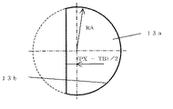
ここで実施例2の光吸収部13cが設けられる位置について、実施例1の図11を用いて説明する。図11(b)に示されたとおり、LED素子30から放射された光線の一部は、主光線25として第1焦点面FP1−1で光軸27と交差して第1のマイクロレンズ12aに入射し、光軸27に略平行な光線として、開口部13aの内壁付近を通過して第2のマイクロレンズ12bに入射する。このとき、LED素子30から放射された光線の一部は、周辺光線26として第1のマイクロレンズ12aに入射し、中間像面MIPと開口部13aの交差する付近であって、マイクロレンズ12の配列方向と略垂直でマイクロレンズ12の光軸27と略垂直な方向におけるLED素子30からXIの位置に像EGを形成する。
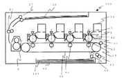
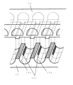
3 LEDヘッド
11a、11b レンズ板
12a、12b マイクロレンズ
13 遮光部材
13a 開口部
13b、13c 光吸収部
30 LED素子
100 電子写真プリンタ
500 スキャナ
Claims (15)
- 複数のマイクロレンズが直線状に配列された複数のレンズ集合体と、
絞りとしての開口部を複数有し、前記複数のレンズ集合体に対して該複数の開口部が前記複数のマイクロレンズにそれぞれ対向するように配設された遮光部材とを有し、
前記レンズ集合体の各マイクロレンズの光軸はレンズ集合体間で対向するマイクロレンズの光軸に略一致するとともに各マイクロレンズの光軸は前記遮光部材の前記開口部を通過し、
前記開口部に光を吸収する光吸収部を設け、
前記光吸収部における可視光全域の全光反射率が0乃至3パーセントであり、
前記レンズ集合体における前記マイクロレンズは、複数のレンズ列を形成するように配列され、前記レンズ列内の前記マイクロレンズの配列間隔をPY、前記レンズ列の配列間隔をPXとしたとき、PX<PYであり、
前記光吸収部は前記マイクロレンズの光軸方向に略平行な略帯状体であり、
前記マイクロレンズの焦点距離をFO、前記マイクロレンズと物体面との距離をLO、前記マイクロレンズの配列方向に略垂直で前記マイクロレンズの光軸に略垂直な方向における物体と前記光軸との距離をXO、前記マイクロレンズの配列方向に略垂直で前記光軸に略垂直な方向における物体と前記光吸収部との距離をXIとしたとき、
であることを特徴とするレンズアレイ。 - 複数のマイクロレンズが直線状に配列された複数のレンズ集合体と、
絞りとしての開口部を複数有し、前記複数のレンズ集合体に対して該複数の開口部が前記複数のマイクロレンズにそれぞれ対向するように配設された遮光部材とを有し、
前記レンズ集合体の各マイクロレンズの光軸はレンズ集合体間で対向するマイクロレンズの光軸に略一致するとともに各マイクロレンズの光軸は前記遮光部材の前記開口部を通過し、
前記開口部に光を吸収する光吸収部を設け、
前記光吸収部における可視光全域の全光反射率が0乃至3パーセントであり、
前記レンズ集合体における前記マイクロレンズは、複数のレンズ列を形成するように配列され、前記レンズ列内の前記マイクロレンズの配列間隔をPY、前記レンズ列の配列間隔をPXとしたとき、PX<PYであり、
前記光吸収部は前記マイクロレンズの光軸方向に略平行な略帯状体であり、
前記マイクロレンズは該マイクロレンズの光軸に対して略垂直な方向に配列間隔PXで2列に配列され、前記マイクロレンズの焦点距離をFO、前記マイクロレンズと物体面との距離をLO、前記マイクロレンズの配列方向に略垂直で前記光軸に略垂直な方向における物体と前記光吸収部との距離をXIとしたとき、
であることを特徴とするレンズアレイ。 - 前記光吸収部における光源の光線の反射率が0乃至3パーセントである請求項1記載のレ
ンズアレイ。 - 前記光吸収部は粗面部により形成される請求項1又は2記載のレンズアレイ。
- 前記光吸収部は前記マイクロレンズの光軸方向の算術平均粗さが2μm乃至20μmである請求項1、2又は4記載のレンズアレイ。
- 前記遮光部材はフィラーを添加した樹脂により形成される請求項1、2又は4記載のレンズアレイ。
- 前記フィラーの大きさは30μm乃至300μmである請求項6記載のレンズアレイ。
- 前記フィラーの添加量は、前記樹脂100重量部に対して10重量部乃至100重量部である請求項6又は7記載のレンズアレイ。
- 前記光吸収部は粗面部が形成された型の形状が転写されている請求項4記載のレンズアレイ。
- 前記光吸収部は光吸収材料の被覆層により形成される請求項4記載のレンズアレイ。
- 互いに隣接する前記マイクロレンズの光軸間の距離をPN、前記マイクロレンズの光軸から外周部までの距離の最大値をRLとしたとき、RL>PN/2である請求項1〜10のいずれかに記載のレンズアレイ。
- 請求項1〜11のいずれかに記載のレンズアレイを用いた露光装置。
- 請求項1〜11のいずれかに記載のレンズアレイを用いたLEDヘッド。
- 請求項1〜11のいずれかに記載のレンズアレイを用いた画像形成装置。
- 請求項1〜11のいずれかに記載のレンズアレイを用いた読取装置。
Priority Applications (2)
| Application Number | Priority Date | Filing Date | Title |
|---|---|---|---|
| JP2008172823A JP4906798B2 (ja) | 2008-07-01 | 2008-07-01 | レンズアレイ、ledヘッド、露光装置、画像形成装置及び読取装置 |
| US12/458,015 US7957067B2 (en) | 2008-07-01 | 2009-06-29 | Lens array, LED head, exposure device, image forming apparatus and reading apparatus |
Applications Claiming Priority (1)
| Application Number | Priority Date | Filing Date | Title |
|---|---|---|---|
| JP2008172823A JP4906798B2 (ja) | 2008-07-01 | 2008-07-01 | レンズアレイ、ledヘッド、露光装置、画像形成装置及び読取装置 |
Publications (2)
| Publication Number | Publication Date |
|---|---|
| JP2010014824A JP2010014824A (ja) | 2010-01-21 |
| JP4906798B2 true JP4906798B2 (ja) | 2012-03-28 |
Family
ID=41464158
Family Applications (1)
| Application Number | Title | Priority Date | Filing Date |
|---|---|---|---|
| JP2008172823A Expired - Fee Related JP4906798B2 (ja) | 2008-07-01 | 2008-07-01 | レンズアレイ、ledヘッド、露光装置、画像形成装置及び読取装置 |
Country Status (2)
| Country | Link |
|---|---|
| US (1) | US7957067B2 (ja) |
| JP (1) | JP4906798B2 (ja) |
Families Citing this family (9)
| Publication number | Priority date | Publication date | Assignee | Title |
|---|---|---|---|---|
| KR101728464B1 (ko) * | 2010-05-11 | 2017-04-19 | 에스프린팅솔루션 주식회사 | 렌즈 어레이, 선형 노광 장치 및 선형 노광 장치를 채용한 광학 장치 |
| JP2012230252A (ja) * | 2011-04-26 | 2012-11-22 | Oki Data Corp | レンズアレイ、レンズユニット、露光装置、画像形成装置、及び読み取り装置 |
| JP2014521992A (ja) | 2011-07-19 | 2014-08-28 | ヘプタゴン・マイクロ・オプティクス・プライベート・リミテッド | 受動光学構成要素の製造方法および受動光学構成要素を備えるデバイス |
| US9461024B2 (en) * | 2013-08-01 | 2016-10-04 | Cree, Inc. | Light emitter devices and methods for light emitting diode (LED) chips |
| EP4462327A3 (en) | 2014-08-20 | 2024-11-20 | Hitachi Energy AG | Configuration of malfunction prediction for components and units of technical entities |
| ES3046836T3 (en) | 2014-08-20 | 2025-12-02 | Hitachi Energy Ag | Malfunction prediction for components and units of technical entities |
| KR20180019500A (ko) | 2015-04-22 | 2018-02-26 | 선전 제노리비전 테크놀로지 컴퍼니, 리미티드 | 생물감지기 |
| WO2021044573A1 (ja) * | 2019-09-05 | 2021-03-11 | 三菱電機株式会社 | 画像読取装置 |
| US11807220B1 (en) | 2023-05-30 | 2023-11-07 | Geotab Inc. | Method for capturing voltage-based events in motor vehicles |
Family Cites Families (9)
| Publication number | Priority date | Publication date | Assignee | Title |
|---|---|---|---|---|
| JPH06252450A (ja) * | 1993-02-23 | 1994-09-09 | Kyocera Corp | 画像装置 |
| US5796522A (en) * | 1996-12-20 | 1998-08-18 | Eastman Kodak Company | Lenslet array system with a baffle structure and a shutter |
| JPH10210213A (ja) * | 1997-01-24 | 1998-08-07 | Fujitsu Ltd | 光学装置 |
| US6707613B2 (en) * | 2000-04-05 | 2004-03-16 | Rohm Co., Ltd. | Lens array unit and method of forming image |
| JP4495942B2 (ja) | 2003-10-20 | 2010-07-07 | リコー光学株式会社 | 結像光学系・画像形成装置・プリンターおよび画像読取装置 |
| JP2006030722A (ja) * | 2004-07-20 | 2006-02-02 | Alps Electric Co Ltd | 光学読取用レンズアレイ及びその製造方法 |
| JPWO2007040246A1 (ja) * | 2005-10-06 | 2009-04-16 | 日本板硝子株式会社 | イメージ結像光学系、イメージ結像光学系を用いた画像読取り装置および画像書込み装置 |
| JP4402674B2 (ja) * | 2006-09-29 | 2010-01-20 | 株式会社沖データ | レンズアレイ、ledヘッド、露光装置及び画像形成装置 |
| JP2010145821A (ja) * | 2008-12-19 | 2010-07-01 | Oki Data Corp | レンズアレイ、ledヘッド、露光装置、画像形成装置および読取装置 |
-
2008
- 2008-07-01 JP JP2008172823A patent/JP4906798B2/ja not_active Expired - Fee Related
-
2009
- 2009-06-29 US US12/458,015 patent/US7957067B2/en not_active Expired - Fee Related
Also Published As
| Publication number | Publication date |
|---|---|
| US7957067B2 (en) | 2011-06-07 |
| JP2010014824A (ja) | 2010-01-21 |
| US20100002307A1 (en) | 2010-01-07 |
Similar Documents
| Publication | Publication Date | Title |
|---|---|---|
| JP4906798B2 (ja) | レンズアレイ、ledヘッド、露光装置、画像形成装置及び読取装置 | |
| JP4856199B2 (ja) | レンズユニット、ledヘッド、露光装置、画像形成装置および読取装置 | |
| JP5030828B2 (ja) | レンズアレイ並びにそれを有するledヘッド、露光装置、画像形成装置及び読取装置 | |
| JP5789499B2 (ja) | レンズアレイ、レンズユニット、ledヘッド、露光装置、画像形成装置及び読取装置 | |
| US8023205B2 (en) | Lens array, light emitting diode head, exposure device, image forming apparatus, and reading apparatus | |
| JP5584262B2 (ja) | レンズユニット、ledヘッド、露光装置、画像形成装置および読取装置 | |
| US8000015B2 (en) | Lens unit, LED head, exposing unit, image forming apparatus, and scanning apparatus | |
| JP4714765B2 (ja) | レンズアレイ、ledプリントヘッド、露光装置、画像形成装置及び読取装置 | |
| JP2010164658A (ja) | レンズアレイ、レンズユニット、ledヘッド、露光装置、画像形成装置および読取装置 | |
| JP4402674B2 (ja) | レンズアレイ、ledヘッド、露光装置及び画像形成装置 | |
| JP2008083576A (ja) | レンズアレイ、露光装置、画像形成装置及び読取装置 | |
| JP2012230252A (ja) | レンズアレイ、レンズユニット、露光装置、画像形成装置、及び読み取り装置 | |
| JP4868612B2 (ja) | 露光装置、ledヘッド、画像形成装置及び読取装置 | |
| JP5222161B2 (ja) | レンズユニット、ledヘッド、露光装置、画像形成装置および読取装置 | |
| JP2010145821A (ja) | レンズアレイ、ledヘッド、露光装置、画像形成装置および読取装置 | |
| JP2013025110A (ja) | レンズアレイ、レンズユニット、ledヘッド、露光装置、画像形成装置、読取装置、レンズアレイ成型用型、及びレンズアレイ製造方法 | |
| JP7003723B2 (ja) | レンズユニット、露光装置、ledヘッド、画像形成装置、及び読取装置 | |
| JP5797014B2 (ja) | レンズユニット、ledヘッド、画像形成装置および読取装置 | |
| JP5775389B2 (ja) | レンズアレイ、レンズユニット、ledヘッド、露光装置、画像形成装置および読取装置 | |
| US7719553B2 (en) | Exposure apparatus and image forming apparatus | |
| JP5216109B2 (ja) | レンズアレイ並びにそれを有する露光装置、画像形成装置及び読取装置 | |
| JP5261220B2 (ja) | レンズアレイ、ledヘッド、露光装置、画像形成装置および読取装置 | |
| JP2009151339A (ja) | レンズアレイ、露光装置、画像形成装置及びledヘッド | |
| JP2010210716A (ja) | レンズユニット、レンズ集合部材、ledヘッド、露光装置、画像形成装置、読取装置およびレンズ集合部材の製造方法 | |
| JP2012247566A (ja) | レンズアレイ、レンズユニット、ledヘッド、露光装置、画像形成装置及び読取装置 |
Legal Events
| Date | Code | Title | Description |
|---|---|---|---|
| A621 | Written request for application examination |
Free format text: JAPANESE INTERMEDIATE CODE: A621 Effective date: 20100309 |
|
| A977 | Report on retrieval |
Free format text: JAPANESE INTERMEDIATE CODE: A971007 Effective date: 20100727 |
|
| A131 | Notification of reasons for refusal |
Free format text: JAPANESE INTERMEDIATE CODE: A131 Effective date: 20100810 |
|
| A521 | Written amendment |
Free format text: JAPANESE INTERMEDIATE CODE: A523 Effective date: 20101008 |
|
| A131 | Notification of reasons for refusal |
Free format text: JAPANESE INTERMEDIATE CODE: A131 Effective date: 20111004 |
|
| A521 | Written amendment |
Free format text: JAPANESE INTERMEDIATE CODE: A523 Effective date: 20111125 |
|
| TRDD | Decision of grant or rejection written | ||
| A01 | Written decision to grant a patent or to grant a registration (utility model) |
Free format text: JAPANESE INTERMEDIATE CODE: A01 Effective date: 20111213 |
|
| A01 | Written decision to grant a patent or to grant a registration (utility model) |
Free format text: JAPANESE INTERMEDIATE CODE: A01 |
|
| A61 | First payment of annual fees (during grant procedure) |
Free format text: JAPANESE INTERMEDIATE CODE: A61 Effective date: 20120110 |
|
| FPAY | Renewal fee payment (event date is renewal date of database) |
Free format text: PAYMENT UNTIL: 20150120 Year of fee payment: 3 |
|
| R150 | Certificate of patent or registration of utility model |
Ref document number: 4906798 Country of ref document: JP Free format text: JAPANESE INTERMEDIATE CODE: R150 Free format text: JAPANESE INTERMEDIATE CODE: R150 |
|
| LAPS | Cancellation because of no payment of annual fees |