JP4898705B2 - 周辺の支持薄膜を含むデータ記録装置及び当該装置の製造方法 - Google Patents
周辺の支持薄膜を含むデータ記録装置及び当該装置の製造方法 Download PDFInfo
- Publication number
- JP4898705B2 JP4898705B2 JP2007550812A JP2007550812A JP4898705B2 JP 4898705 B2 JP4898705 B2 JP 4898705B2 JP 2007550812 A JP2007550812 A JP 2007550812A JP 2007550812 A JP2007550812 A JP 2007550812A JP 4898705 B2 JP4898705 B2 JP 4898705B2
- Authority
- JP
- Japan
- Prior art keywords
- thin film
- substrate
- flexible
- microdots
- fixed
- Prior art date
- Legal status (The legal status is an assumption and is not a legal conclusion. Google has not performed a legal analysis and makes no representation as to the accuracy of the status listed.)
- Expired - Fee Related
Links
- 239000010409 thin film Substances 0.000 title claims description 46
- 238000004519 manufacturing process Methods 0.000 title claims description 7
- 230000002093 peripheral effect Effects 0.000 title description 2
- 238000003860 storage Methods 0.000 claims description 47
- 239000000758 substrate Substances 0.000 claims description 34
- VAYOSLLFUXYJDT-RDTXWAMCSA-N Lysergic acid diethylamide Chemical compound C1=CC(C=2[C@H](N(C)C[C@@H](C=2)C(=O)N(CC)CC)C2)=C3C2=CNC3=C1 VAYOSLLFUXYJDT-RDTXWAMCSA-N 0.000 claims description 32
- 238000000034 method Methods 0.000 claims description 14
- 239000000463 material Substances 0.000 claims description 8
- XUIMIQQOPSSXEZ-UHFFFAOYSA-N Silicon Chemical compound [Si] XUIMIQQOPSSXEZ-UHFFFAOYSA-N 0.000 claims description 6
- 229910052710 silicon Inorganic materials 0.000 claims description 6
- 239000010703 silicon Substances 0.000 claims description 6
- 238000005530 etching Methods 0.000 claims description 5
- UMIVXZPTRXBADB-UHFFFAOYSA-N benzocyclobutene Chemical compound C1=CC=C2CCC2=C1 UMIVXZPTRXBADB-UHFFFAOYSA-N 0.000 claims description 3
- 239000012528 membrane Substances 0.000 claims description 3
- 239000010408 film Substances 0.000 claims description 2
- 239000011347 resin Substances 0.000 claims description 2
- 229920005989 resin Polymers 0.000 claims description 2
- 238000004528 spin coating Methods 0.000 claims description 2
- 238000003892 spreading Methods 0.000 claims 1
- 238000000151 deposition Methods 0.000 description 4
- 230000008021 deposition Effects 0.000 description 4
- 230000000694 effects Effects 0.000 description 3
- CFAKWWQIUFSQFU-UHFFFAOYSA-N 2-hydroxy-3-methylcyclopent-2-en-1-one Chemical compound CC1=C(O)C(=O)CC1 CFAKWWQIUFSQFU-UHFFFAOYSA-N 0.000 description 2
- 238000003491 array Methods 0.000 description 2
- 238000003486 chemical etching Methods 0.000 description 2
- 238000007796 conventional method Methods 0.000 description 2
- 238000001659 ion-beam spectroscopy Methods 0.000 description 2
- 229920000642 polymer Polymers 0.000 description 2
- 239000001837 2-hydroxy-3-methylcyclopent-2-en-1-one Substances 0.000 description 1
- 229910052581 Si3N4 Inorganic materials 0.000 description 1
- 230000002411 adverse Effects 0.000 description 1
- 230000015572 biosynthetic process Effects 0.000 description 1
- 238000001312 dry etching Methods 0.000 description 1
- 230000006870 function Effects 0.000 description 1
- 238000002844 melting Methods 0.000 description 1
- 230000008018 melting Effects 0.000 description 1
- 238000004377 microelectronic Methods 0.000 description 1
- 238000000206 photolithography Methods 0.000 description 1
- 238000001020 plasma etching Methods 0.000 description 1
- 238000005498 polishing Methods 0.000 description 1
- 238000003825 pressing Methods 0.000 description 1
- HQVNEWCFYHHQES-UHFFFAOYSA-N silicon nitride Chemical compound N12[Si]34N5[Si]62N3[Si]51N64 HQVNEWCFYHHQES-UHFFFAOYSA-N 0.000 description 1
- 125000006850 spacer group Chemical group 0.000 description 1
- 239000000126 substance Substances 0.000 description 1
Images
Classifications
-
- G—PHYSICS
- G11—INFORMATION STORAGE
- G11B—INFORMATION STORAGE BASED ON RELATIVE MOVEMENT BETWEEN RECORD CARRIER AND TRANSDUCER
- G11B9/00—Recording or reproducing using a method not covered by one of the main groups G11B3/00 - G11B7/00; Record carriers therefor
- G11B9/12—Recording or reproducing using a method not covered by one of the main groups G11B3/00 - G11B7/00; Record carriers therefor using near-field interactions; Record carriers therefor
- G11B9/14—Recording or reproducing using a method not covered by one of the main groups G11B3/00 - G11B7/00; Record carriers therefor using near-field interactions; Record carriers therefor using microscopic probe means, i.e. recording or reproducing by means directly associated with the tip of a microscopic electrical probe as used in Scanning Tunneling Microscopy [STM] or Atomic Force Microscopy [AFM] for inducing physical or electrical perturbations in a recording medium; Record carriers or media specially adapted for such transducing of information
- G11B9/1418—Disposition or mounting of heads or record carriers
-
- B—PERFORMING OPERATIONS; TRANSPORTING
- B82—NANOTECHNOLOGY
- B82Y—SPECIFIC USES OR APPLICATIONS OF NANOSTRUCTURES; MEASUREMENT OR ANALYSIS OF NANOSTRUCTURES; MANUFACTURE OR TREATMENT OF NANOSTRUCTURES
- B82Y10/00—Nanotechnology for information processing, storage or transmission, e.g. quantum computing or single electron logic
Landscapes
- Engineering & Computer Science (AREA)
- Chemical & Material Sciences (AREA)
- Nanotechnology (AREA)
- Physics & Mathematics (AREA)
- Mathematical Physics (AREA)
- Theoretical Computer Science (AREA)
- Crystallography & Structural Chemistry (AREA)
- Micromachines (AREA)
Description
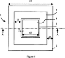
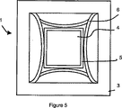
−記憶媒体1の寸法c1は約15mm
−薄膜4の寸法c2は約9.5mm
−内部フレーム5の幅l1は約0.25mm
−外部フレーム3の幅l2は約0.5mm
−固定薄膜6の幅l3は約2mm
Claims (11)
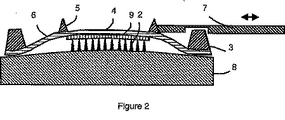
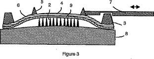
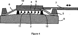
- 基板(8)と、
前記基板(8)上に配置されるナノメータ規模のマイクロドット(2)の2次元アレイと、
前記マイクロドット(2)に面する記憶層(9)と、
前記記憶層(9)を覆う可撓性薄膜(4)と、
前記可撓性薄膜(4)を外部フレーム(3)上へ固定し、且つ、前記基板(8)に沿った面で前記可撓性薄膜(4)の移動を可能にする可撓性固定手段を備え、
前記可撓性固定手段は、前記可撓性薄膜(4)の周辺に広がる固定薄膜(6)によって形成され、且つ、前記基板(8)に対して垂直に前記可撓性薄膜(4)の移動を可能にする、ことを特徴とするデータ記録装置。 - 前記可撓性薄膜(4)及び前記固定薄膜(6)は、プラスチック材料から作られることを特徴とする請求項1に記載の装置。
- 前記プラスチック材料は、ベンゾシクロブテンベース樹脂であることを特徴とする請求項2に記載の装置。
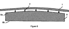
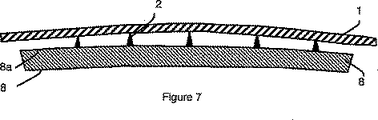
- 前記マイクロドット(2)は、前記基板(8)の凸状の前面(8a)に直接形成されることを特徴とする請求項1乃至3の何れか1項に記載の装置。
- 前記凸状の前面(8a)は、1m〜5mに含まれる曲線半径を有する請求項4に記載の装置。
- 前記マイクロドット(2)をアドレッシングし、且つ、制御する、電気的手段(5)が、前記基板(8)に集積されることを特徴とする請求項4又は5に記載の装置。
- 前記可撓性薄膜(4)及び前記固定薄膜(6)は、同時に形成されることを特徴とする請求項1乃至6の何れか1項に記載の装置の製造方法。
- 前記可撓性薄膜(4)及び前記固定薄膜(6)は、シリコンウェハ上のプラスチック材料のスピンコーティングによって形成されることを特徴とする請求項7に記載の方法。
- 前記固定薄膜(6)の表面の一部を除去するエッチングステップを含むことを特徴とする請求項7に記載の方法。
- 前記外部フレーム(3)と、前記固定薄膜(6)の輪郭を描く内部フレーム(5)と、を形成するシリコンウェハのエッチングステップを含むことを特徴とする請求項8又は9に記載の方法。
- 前記外部フレーム(3)と、前記可撓性薄膜(4)の支持領域(10)と、を形成するシリコンウェハのエッチングステップを含むことを特徴とする請求項8又は9に記載の方法。
Applications Claiming Priority (3)
| Application Number | Priority Date | Filing Date | Title |
|---|---|---|---|
| FR0500471A FR2880979B1 (fr) | 2005-01-17 | 2005-01-17 | Dispositif d'enregistrement de donnees comportant une membrane peripherique de support et procede de fabrication |
| FR0500471 | 2005-01-17 | ||
| PCT/FR2005/003261 WO2006075066A1 (fr) | 2005-01-17 | 2005-12-22 | Dispositif d'enregistrement de donnees comportant une membrane peripherique de support et procede de fabrication |
Publications (2)
| Publication Number | Publication Date |
|---|---|
| JP2008527606A JP2008527606A (ja) | 2008-07-24 |
| JP4898705B2 true JP4898705B2 (ja) | 2012-03-21 |
Family
ID=34954845
Family Applications (1)
| Application Number | Title | Priority Date | Filing Date |
|---|---|---|---|
| JP2007550812A Expired - Fee Related JP4898705B2 (ja) | 2005-01-17 | 2005-12-22 | 周辺の支持薄膜を含むデータ記録装置及び当該装置の製造方法 |
Country Status (5)
| Country | Link |
|---|---|
| US (1) | US7898931B2 (ja) |
| EP (1) | EP1839304A1 (ja) |
| JP (1) | JP4898705B2 (ja) |
| FR (1) | FR2880979B1 (ja) |
| WO (1) | WO2006075066A1 (ja) |
Families Citing this family (1)
| Publication number | Priority date | Publication date | Assignee | Title |
|---|---|---|---|---|
| US9221678B2 (en) * | 2008-10-06 | 2015-12-29 | University Of Florida Research Foundation, Inc. | Active fixturing for micro/mesoscale, machine tool systems |
Citations (2)
| Publication number | Priority date | Publication date | Assignee | Title |
|---|---|---|---|---|
| JPH1040597A (ja) * | 1996-07-25 | 1998-02-13 | Tdk Corp | メモリー装置 |
| JP2000152596A (ja) * | 1998-10-30 | 2000-05-30 | Internatl Business Mach Corp <Ibm> | 少なくとも2つの自由度を有する磁気走査または位置決めシステム |
Family Cites Families (10)
| Publication number | Priority date | Publication date | Assignee | Title |
|---|---|---|---|---|
| US5216631A (en) * | 1990-11-02 | 1993-06-01 | Sliwa Jr John W | Microvibratory memory device |
| FR2757992B1 (fr) * | 1996-12-26 | 1999-01-29 | Commissariat Energie Atomique | Support d'enregistrement d'informations, dispositif de lecture de ce support et procedes de mise en oeuvre de ce dispositif |
| EP1168334B1 (en) * | 2000-06-26 | 2006-03-08 | Samsung Electronics Co. Ltd. | Electromagnetic X-Y stage driver for nano data storage system and method for fabricating coils of the same |
| JP2002092946A (ja) * | 2000-09-20 | 2002-03-29 | Toshiba Corp | 光ディスク基板およびその製造方法 |
| US6522566B2 (en) * | 2000-12-01 | 2003-02-18 | Hewlett-Packard Company | System modules with atomic resolution storage memory |
| US7018572B2 (en) * | 2001-06-11 | 2006-03-28 | General Electric Company | Method for producing data storage media |
| FR2845513B1 (fr) | 2002-10-03 | 2006-08-11 | Commissariat Energie Atomique | Dispositif d'enregistrement de donnees comportant un support de memoire en forme de membrane |
| FR2856184B1 (fr) | 2003-06-13 | 2008-04-11 | Commissariat Energie Atomique | Dispositif d'enregistrement de donnees comportant des micro-pointes et un support d'enregistrement |
| JP2005004921A (ja) * | 2003-06-13 | 2005-01-06 | Alps Electric Co Ltd | 高精度位置決め装置 |
| WO2005013270A1 (fr) | 2003-07-03 | 2005-02-10 | Commissariat A L'energie Atomique | Procede d’enregistrement de donnees et dispositif de mise en oeuvre comportant un support de memoire deformable |
-
2005
- 2005-01-17 FR FR0500471A patent/FR2880979B1/fr not_active Expired - Fee Related
- 2005-12-22 US US11/794,007 patent/US7898931B2/en not_active Expired - Fee Related
- 2005-12-22 WO PCT/FR2005/003261 patent/WO2006075066A1/fr not_active Ceased
- 2005-12-22 EP EP05850600A patent/EP1839304A1/fr not_active Withdrawn
- 2005-12-22 JP JP2007550812A patent/JP4898705B2/ja not_active Expired - Fee Related
Patent Citations (2)
| Publication number | Priority date | Publication date | Assignee | Title |
|---|---|---|---|---|
| JPH1040597A (ja) * | 1996-07-25 | 1998-02-13 | Tdk Corp | メモリー装置 |
| JP2000152596A (ja) * | 1998-10-30 | 2000-05-30 | Internatl Business Mach Corp <Ibm> | 少なくとも2つの自由度を有する磁気走査または位置決めシステム |
Also Published As
| Publication number | Publication date |
|---|---|
| JP2008527606A (ja) | 2008-07-24 |
| FR2880979B1 (fr) | 2007-03-16 |
| EP1839304A1 (fr) | 2007-10-03 |
| FR2880979A1 (fr) | 2006-07-21 |
| US20080095021A1 (en) | 2008-04-24 |
| WO2006075066A1 (fr) | 2006-07-20 |
| US7898931B2 (en) | 2011-03-01 |
Similar Documents
| Publication | Publication Date | Title |
|---|---|---|
| TW519702B (en) | Planarization process for semiconductor substrates | |
| US7570416B2 (en) | Method and apparatus for a reflective spatial light modulator with a flexible pedestal | |
| US7245358B2 (en) | Substrate support system | |
| JP2013538446A (ja) | 湾曲圧電膜を有するデバイスの形成 | |
| EP0784847B1 (en) | A memory device | |
| JP2001060618A (ja) | 基板吸着保持方法、基板吸着保持装置および該基板吸着保持装置を用いた露光装置ならびにデバイスの製造方法 | |
| US7101272B2 (en) | Carrier head for thermal drift compensation | |
| CN105934711A (zh) | 用于改进的覆盖纠正的低接触式压印光刻术模板卡盘系统 | |
| JP3935976B2 (ja) | 半導体層構造および大容量メモリ装置の記録媒体 | |
| CN101923215A (zh) | 用于形成复合基底结构的方法 | |
| JP4898705B2 (ja) | 周辺の支持薄膜を含むデータ記録装置及び当該装置の製造方法 | |
| US20130001719A1 (en) | Interaction structure for a storage medium | |
| KR101587780B1 (ko) | 화학 기계적 연마 장치용 캐리어 헤드의 멤브레인 | |
| JP4494337B2 (ja) | ダイヤフラム型支持体を有するデータ記録装置 | |
| JP2008527605A (ja) | 凸状表面を成す自由端を有するマイクロドットを備えたデータ記録装置及び当該装置の製造方法 | |
| JP2007516544A (ja) | データ記録方法及びこの方法を実施する、変形可能なメモリ支持体を有する装置 | |
| JP2006502523A5 (ja) | ||
| JP5044384B2 (ja) | 光学素子および光学機能素子 | |
| JP4294399B2 (ja) | 熱電変換デバイスの製造方法 | |
| JP2013049112A (ja) | ポリシングパッド及びその製造方法 | |
| TW202318492A (zh) | 使用多方向性致動膜調整晶圓形狀的方法 | |
| JP3699950B2 (ja) | ウエハ研磨装置 | |
| Sreenivasan et al. | Substrate support system |
Legal Events
| Date | Code | Title | Description |
|---|---|---|---|
| A621 | Written request for application examination |
Free format text: JAPANESE INTERMEDIATE CODE: A621 Effective date: 20081201 |
|
| A977 | Report on retrieval |
Free format text: JAPANESE INTERMEDIATE CODE: A971007 Effective date: 20101007 |
|
| A131 | Notification of reasons for refusal |
Free format text: JAPANESE INTERMEDIATE CODE: A131 Effective date: 20101015 |
|
| A521 | Request for written amendment filed |
Free format text: JAPANESE INTERMEDIATE CODE: A523 Effective date: 20110114 |
|
| A131 | Notification of reasons for refusal |
Free format text: JAPANESE INTERMEDIATE CODE: A131 Effective date: 20110527 |
|
| A521 | Request for written amendment filed |
Free format text: JAPANESE INTERMEDIATE CODE: A523 Effective date: 20110823 |
|
| TRDD | Decision of grant or rejection written | ||
| A01 | Written decision to grant a patent or to grant a registration (utility model) |
Free format text: JAPANESE INTERMEDIATE CODE: A01 Effective date: 20111129 |
|
| A01 | Written decision to grant a patent or to grant a registration (utility model) |
Free format text: JAPANESE INTERMEDIATE CODE: A01 |
|
| A61 | First payment of annual fees (during grant procedure) |
Free format text: JAPANESE INTERMEDIATE CODE: A61 Effective date: 20111226 |
|
| R150 | Certificate of patent or registration of utility model |
Free format text: JAPANESE INTERMEDIATE CODE: R150 |
|
| FPAY | Renewal fee payment (event date is renewal date of database) |
Free format text: PAYMENT UNTIL: 20150106 Year of fee payment: 3 |
|
| LAPS | Cancellation because of no payment of annual fees |