JP4898705B2 - Data recording apparatus including peripheral supporting thin film and method of manufacturing the apparatus - Google Patents
Data recording apparatus including peripheral supporting thin film and method of manufacturing the apparatus Download PDFInfo
- Publication number
- JP4898705B2 JP4898705B2 JP2007550812A JP2007550812A JP4898705B2 JP 4898705 B2 JP4898705 B2 JP 4898705B2 JP 2007550812 A JP2007550812 A JP 2007550812A JP 2007550812 A JP2007550812 A JP 2007550812A JP 4898705 B2 JP4898705 B2 JP 4898705B2
- Authority
- JP
- Japan
- Prior art keywords
- thin film
- substrate
- flexible
- microdots
- fixed
- Prior art date
- Legal status (The legal status is an assumption and is not a legal conclusion. Google has not performed a legal analysis and makes no representation as to the accuracy of the status listed.)
- Expired - Fee Related
Links
- 239000010409 thin film Substances 0.000 title claims description 46
- 238000004519 manufacturing process Methods 0.000 title claims description 7
- 230000002093 peripheral effect Effects 0.000 title description 2
- 238000003860 storage Methods 0.000 claims description 47
- 239000000758 substrate Substances 0.000 claims description 34
- VAYOSLLFUXYJDT-RDTXWAMCSA-N Lysergic acid diethylamide Chemical compound C1=CC(C=2[C@H](N(C)C[C@@H](C=2)C(=O)N(CC)CC)C2)=C3C2=CNC3=C1 VAYOSLLFUXYJDT-RDTXWAMCSA-N 0.000 claims description 32
- 238000000034 method Methods 0.000 claims description 14
- 239000000463 material Substances 0.000 claims description 8
- XUIMIQQOPSSXEZ-UHFFFAOYSA-N Silicon Chemical compound [Si] XUIMIQQOPSSXEZ-UHFFFAOYSA-N 0.000 claims description 6
- 229910052710 silicon Inorganic materials 0.000 claims description 6
- 239000010703 silicon Substances 0.000 claims description 6
- 238000005530 etching Methods 0.000 claims description 5
- UMIVXZPTRXBADB-UHFFFAOYSA-N benzocyclobutene Chemical compound C1=CC=C2CCC2=C1 UMIVXZPTRXBADB-UHFFFAOYSA-N 0.000 claims description 3
- 239000012528 membrane Substances 0.000 claims description 3
- 239000010408 film Substances 0.000 claims description 2
- 239000011347 resin Substances 0.000 claims description 2
- 229920005989 resin Polymers 0.000 claims description 2
- 238000004528 spin coating Methods 0.000 claims description 2
- 238000003892 spreading Methods 0.000 claims 1
- 238000000151 deposition Methods 0.000 description 4
- 230000008021 deposition Effects 0.000 description 4
- 230000000694 effects Effects 0.000 description 3
- CFAKWWQIUFSQFU-UHFFFAOYSA-N 2-hydroxy-3-methylcyclopent-2-en-1-one Chemical compound CC1=C(O)C(=O)CC1 CFAKWWQIUFSQFU-UHFFFAOYSA-N 0.000 description 2
- 238000003491 array Methods 0.000 description 2
- 238000003486 chemical etching Methods 0.000 description 2
- 238000007796 conventional method Methods 0.000 description 2
- 238000001659 ion-beam spectroscopy Methods 0.000 description 2
- 229920000642 polymer Polymers 0.000 description 2
- 239000001837 2-hydroxy-3-methylcyclopent-2-en-1-one Substances 0.000 description 1
- 229910052581 Si3N4 Inorganic materials 0.000 description 1
- 230000002411 adverse Effects 0.000 description 1
- 230000015572 biosynthetic process Effects 0.000 description 1
- 238000001312 dry etching Methods 0.000 description 1
- 230000006870 function Effects 0.000 description 1
- 238000002844 melting Methods 0.000 description 1
- 230000008018 melting Effects 0.000 description 1
- 238000004377 microelectronic Methods 0.000 description 1
- 238000000206 photolithography Methods 0.000 description 1
- 238000001020 plasma etching Methods 0.000 description 1
- 238000005498 polishing Methods 0.000 description 1
- 238000003825 pressing Methods 0.000 description 1
- HQVNEWCFYHHQES-UHFFFAOYSA-N silicon nitride Chemical compound N12[Si]34N5[Si]62N3[Si]51N64 HQVNEWCFYHHQES-UHFFFAOYSA-N 0.000 description 1
- 125000006850 spacer group Chemical group 0.000 description 1
- 239000000126 substance Substances 0.000 description 1
Images
Classifications
-
- G—PHYSICS
- G11—INFORMATION STORAGE
- G11B—INFORMATION STORAGE BASED ON RELATIVE MOVEMENT BETWEEN RECORD CARRIER AND TRANSDUCER
- G11B9/00—Recording or reproducing using a method not covered by one of the main groups G11B3/00 - G11B7/00; Record carriers therefor
- G11B9/12—Recording or reproducing using a method not covered by one of the main groups G11B3/00 - G11B7/00; Record carriers therefor using near-field interactions; Record carriers therefor
- G11B9/14—Recording or reproducing using a method not covered by one of the main groups G11B3/00 - G11B7/00; Record carriers therefor using near-field interactions; Record carriers therefor using microscopic probe means, i.e. recording or reproducing by means directly associated with the tip of a microscopic electrical probe as used in Scanning Tunneling Microscopy [STM] or Atomic Force Microscopy [AFM] for inducing physical or electrical perturbations in a recording medium; Record carriers or media specially adapted for such transducing of information
- G11B9/1418—Disposition or mounting of heads or record carriers
-
- B—PERFORMING OPERATIONS; TRANSPORTING
- B82—NANOTECHNOLOGY
- B82Y—SPECIFIC USES OR APPLICATIONS OF NANOSTRUCTURES; MEASUREMENT OR ANALYSIS OF NANOSTRUCTURES; MANUFACTURE OR TREATMENT OF NANOSTRUCTURES
- B82Y10/00—Nanotechnology for information processing, storage or transmission, e.g. quantum computing or single electron logic
Landscapes
- Engineering & Computer Science (AREA)
- Chemical & Material Sciences (AREA)
- Nanotechnology (AREA)
- Physics & Mathematics (AREA)
- Mathematical Physics (AREA)
- Theoretical Computer Science (AREA)
- Crystallography & Structural Chemistry (AREA)
- Micromachines (AREA)
Description
本発明は、記憶媒体に面して設けられたナノメータ規模のマイクロドットの2次元アレイと、その平面の感応領域の移動を可能にする外部フレーム上に記憶媒体の感応領域を固定する可撓性固定手段と、を含むデータ記録装置に関する。 The present invention provides a two-dimensional array of nanometer-scale microdots facing a storage medium and the flexibility to fix the sensitive area of the storage medium on an external frame that allows movement of the planar sensitive area A data recording apparatus including a fixing means.
本発明は、そのような装置の製造方法にも関する。 The invention also relates to a method of manufacturing such a device.
データ記録分野では、極めて大きな記憶容量が、ナノメータサイズの頂点を有するマイクロドットのアレイを改良することによって近年達成されてきた。電気機械であり得るアクチュエータは、記憶媒体を構成する媒体の面に対してマイクロドット全体のアレイの完全に統制される相対的な移動を可能にする。 In the data recording field, very large storage capacities have been achieved in recent years by improving arrays of microdots with nanometer-sized vertices. Actuators, which can be electromechanical, allow for a fully controlled relative movement of the entire array of microdots relative to the surface of the medium making up the storage medium.
頂点効果(tip effect)を伴うそのようなデータ記録装置では、全てのマイクロドットと記憶媒体の感応領域(記録領域)の完全なコンタクトが保証されなければならない。各マイクロドットの位置を個別に制御することは、システムの複雑性から予想不可能である。しかしながら、マイクロドットは、マイクロエレクトロニクスの技術から導き出される技術によって集合的な方法で製造され、製造に起因してマイクロドットの高さのばらつきが常に残る。このばらつきは極めて小さく、典型的には約100nmであるが、格子のマイクロドットの最も長いものは、他のものよりも記憶媒体を圧迫する。 In such a data recording device with a tip effect, complete contact between all microdots and the sensitive area (recording area) of the storage medium must be ensured. Controlling the position of each microdot individually is unpredictable due to the complexity of the system. However, microdots are manufactured in a collective manner by techniques derived from microelectronics techniques, and microdot height variations always remain due to manufacturing. This variation is very small, typically about 100 nm, but the longest of the microdots in the grid presses the storage medium more than the others.
この問題を克服するために、各マイクロドットは、近視野の顕微鏡を操作するのに用いられるマイクロドットアレイと同じように、カンチレバーの一端が張り出すことで支持される。そのとき、カンチレバーの可撓性は、押圧の応力を吸収可能にする。 To overcome this problem, each microdot is supported by overhanging one end of the cantilever, similar to a microdot array used to operate a near field microscope. The flexibility of the cantilever then makes it possible to absorb the pressing stress.
文献「“Filling the Memory Access Gap: A Case for On−Chip Magnetic Storage”、Steven W. Schlosser著、Technical Report CMU−CS−99−174, School of Computer Science, Carnegie Mellon University、1999年11月出版」は、可撓性固定部によってマイクロドットを支持する基板に対するフレーム全体に接続される記憶媒体を伴うカンチレバーとマイクロドットのアレイの連携について説明する。記憶媒体の感応領域は、その結果、2つの垂直方向に動作するアクチュエータによってそれぞれ自身の平面に移動される。例えば、記憶媒体の移動は、各方向に約100μmであっても良い。数nN単位の接触力を制御するのと同時に、ミリメータ規模の素子(記憶媒体及びマイクロドットアレイ)は、ナノメータ精度で整列されなければならない。しかしながら、接面の平面性及び並列性は、それぞれ50nm以下及び1μラジアン以下の許容値を暗示する。上記文献では、カンチレバー及び高価な動的整列プロセスを用いることによって、このことが可能になる。さらに、この文献に示される関節でつながった平行四辺形型の複雑な可撓性固定部は、多数の技術的ステップを必要とするので、高価である。そのような構造は、表現の程度で影響が与えられる高い機械的応力に起因するほど強くなくても良い。 Literature “Filling the Memory Access Gap: A Case for On-Chip Magnetic Storage”, Steven W. Schlosser, 1999, Technical Report CMU-CS-99-174, Scholen. Describes the cooperation of a microdot array with a cantilever with a storage medium connected to the entire frame for a substrate that supports the microdots by a flexible fixture. The sensitive area of the storage medium is consequently moved to its own plane by two vertically moving actuators. For example, the movement of the storage medium may be about 100 μm in each direction. At the same time as controlling contact forces of a few nN units, millimeter-scale elements (storage media and microdot arrays) must be aligned with nanometer accuracy. However, the flatness and parallelism of the tangent surface implies tolerances of 50 nm or less and 1 μradian or less, respectively. In the above document, this is made possible by using cantilevers and expensive dynamic alignment processes. Furthermore, the parallelogram-shaped complex flexible anchors connected by the joints described in this document are expensive because they require a number of technical steps. Such a structure may not be so strong that it results from high mechanical stresses that are affected by the degree of expression.
他の解決手段は、補償されるマイクロドットの高さ方向のばらつきを可能にする可撓性薄膜を含む記憶媒体の利用に基づいて出願人によって提案されてきた。そのとき、マイクロドットは、カンチレバーなしに、集積もされるアドレッシング回路及び制御回路内の1つのベース基板上に直接的に形成される。マイクロドットのアドレッシング回路及び制御回路のこの完全に統制された製造は、装置のコストを低減することを可能にする。 Other solutions have been proposed by the applicant based on the use of a storage medium that includes a flexible thin film that allows height variations in the compensated microdots. At that time, the microdots are formed directly on one base substrate in the addressing circuit and the control circuit which are also integrated without a cantilever. This fully controlled manufacturing of the microdot addressing and control circuits makes it possible to reduce the cost of the device.
このように、文献WO−A−2004/032132は、各リセスが少なくとも1つのマイクロドットに関連付けられるような複数のリセスを形成するフレームによって支持される可撓性薄膜を含む記憶媒体について説明する。占有率を低減するエッジ効果を取り除くために、記憶媒体は、瓦状に重なったフレームを伴う二重薄膜を含んでも良い。 Thus, document WO-A-2004 / 032132 describes a storage medium comprising a flexible thin film supported by a frame forming a plurality of recesses, each recess being associated with at least one microdot. In order to remove the edge effect that reduces the occupancy, the storage medium may include a double thin film with a frame that is tiled.
文献WO−A−2005/013270では、記憶媒体は、例えば、ポリマーの可撓性層によって形成され、マイクロドットの高さ方向のばらつきを吸収する変形可能な記憶層を含む。 In document WO-A-2005 / 013270, the storage medium comprises a deformable storage layer formed, for example, by a flexible layer of polymer and absorbing the variation in the height direction of the microdots.
このアプローチは、マイクロドットの局部的な高さ方向のばらつきを吸収するには効果的であるが、接触力を克服するのと同時に、全てのマイクロドットを記憶媒体に接触させることを常に保証することはできない。このタイプの問題は、装置を組み立てる間又は熱的ドリフトに起因する変形の後に、マイクロドットを支持する基板の前面が部分的にくぼんでいる場合に特に生じる。 This approach is effective in absorbing the local height variation of the microdots, but always ensures that all microdots are in contact with the storage medium while overcoming the contact force. It is not possible. This type of problem occurs particularly when the front surface of the substrate supporting the microdots is partially recessed during assembly of the device or after deformation due to thermal drift.
本発明の目的は、これらの欠点を示さないデータ記録装置、とりわけ、マイクロドットと記憶媒体の間の良好なコンタクトを保証できるより安価な装置を提供することである。 The object of the present invention is to provide a data recording device which does not exhibit these drawbacks, in particular a cheaper device which can guarantee good contact between the microdots and the storage medium.
本発明によれば、この目的は、添付の特許請求の範囲に記載の装置、とりわけ、可撓性固定手段がその周辺で感応領域を広げ、その平面に対して垂直な感応領域の移動を可能にする可撓性固定薄膜によって形成されるという事実によって達成される。 According to the invention, this object is achieved by the device according to the appended claims, in particular by a flexible fixing means which widens the sensitive area around it and allows the movement of the sensitive area perpendicular to its plane. Achieved by the fact that it is formed by a flexible fixed thin film.
記憶媒体の感応領域は、好ましくは、可撓性固定薄膜によってその周辺に広がる可撓性薄膜を含む。 The sensitive area of the storage medium preferably comprises a flexible thin film extending around it by a flexible fixed thin film.
本発明は、そのようなデータ記録装置の製造方法、とりわけ、可撓性薄膜を含み、可撓性薄膜及び固定薄膜が1つの部分に同時に形成される記憶媒体の感応領域の製造方法に関する。 The present invention relates to a method for manufacturing such a data recording apparatus, and more particularly to a method for manufacturing a sensitive region of a storage medium including a flexible thin film, in which the flexible thin film and the fixed thin film are simultaneously formed in one part.
その他の利点及び特徴は、非限定的な例示のみを目的として与えられた以下の本発明の特定の実施例の記述及び添付の図面からより明らかになるであろう。 Other advantages and features will become more apparent from the following description of specific embodiments of the invention and the accompanying drawings, given by way of non-limiting illustration only.
データ記録装置は、マイクロドット2のアレイと共に記憶媒体1を慣習的に含む。上記文献では、記憶媒体1の感応領域は、その平面内で感応領域が移動できるように外部フレーム3上に可撓的に固定される。
The data recording device conventionally includes a
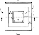
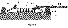
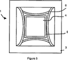
図1〜3及び5では、文献WO−A−2004/032132のように、記憶媒体の感応領域は、内部フレーム5によって輪郭が描かれ、少なくとも1つのセルを形成する可撓性薄膜4を含む。明確化のために、図1及び2は、内部フレーム5によってその周辺で輪郭が描かれた単一セルを示す。実際には、セルはいくつでも良く、各セルは、好ましくは、正方形、長方形又は六角形形状を有し、薄膜は、瓦状に重なった二重薄膜でも良い。
In FIGS. 1 to 3 and 5, as in document WO-A-2004 / 032132, the sensitive area of the storage medium comprises a flexible
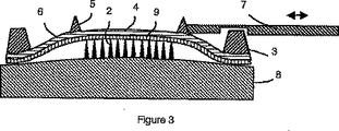
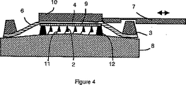
図1〜5に図示されるように、記憶媒体の感応領域は、感応領域を広げる可撓性固定薄膜6、とりわけ、可撓性薄膜4によって外部フレーム3上に可撓的にその周辺に固定される。記憶媒体(マイクロドットを伴うコンタクトになるように設けられた)の前面の可撓性薄膜4、場合によっては固定薄膜6(図3)も覆う記憶層9が記憶媒体を完成させる。図1〜3及び5では、薄膜4は、単に内部フレーム5によって輪郭が描かれ、マイクロドット2は、基板8上に直接的に形成される。図4では、一方、薄膜4は、記憶媒体の背面上の支持領域10によって覆われる。後者の場合には、感応領域は、例えば、カンチレバー11を形成する基板8上への各マイクロドットの可撓性支持素子を固定することを必要とする半剛体である。媒体を構成する記憶層9とその読み出し回路の間の最小限のスペーサを保証するためには、基板8上にスペーシングパッド12を形成することが望ましい。
As shown in FIGS. 1 to 5, the sensitive area of the storage medium is flexibly fixed on the
薄膜4及び6は、任意の適切な方法によって1つの部分に同時に形成されても良い。従って、記憶媒体の背面を構成するシリコンウェハ上のスピンコーティングによって、遠心力によって広がるプラスチック材料を堆積することができる。用いられるプラスチック材料は、好ましくは、ポリマー、とりわけ、CYCLOTENETMのようなベンゾシクロブテン(BCB)樹脂である。
The
薄膜4及び6を形成するプラスチック材料、場合によっては記憶層9の堆積の後に、外部フレーム3及び内部フレーム5又は支持領域10が従来の方法(フォトリソグラフィ、ドライエッチング又はケミカルエッチング…)で得られる。例えば、フレーム3及び5は、シリコンウェハ内において、薄膜4及び6を形成する層を貫いて記憶媒体の背面から異方性ケミカルエッチングすることによって得られる。これらのステップ(薄膜の生成、記憶層の生成及びフレームの生成)の順番は、用いられる材料に関するプロセス制約に依存して必要に応じて反転されても良い。
After the deposition of the plastic material forming the
プラスチック材料の層上に形成される記憶層9は、任意の型式、とりわけ、文献FR−A−2856184に記載される型式であっても良い。
The
図2〜4に示されるように、感応領域がマイクロドット2に圧迫されることを保証し且つ内部フレーム5又は支持領域10と連動して処理するアクチュエータ7(1つのアクチュエータ7は図2〜4に示される)の動作に起因するそれ自身の平面内の感応領域の可撓的移動を可能にするための移動の自由度を後者に与えるのと同時に、固定薄膜6は、このように可撓性薄膜4を含む記憶媒体の感応領域のための支持構造としての役割を果たす外薄膜の一種を構成する。周辺の固定薄膜6の寸法は、その剛性を確定する。その厚さは、好ましくは、約数μであり、その幅は約数mmである。
As shown in FIGS. 2 to 4, an actuator 7 (one actuator 7 is shown in FIGS. At the same time, the
固定薄膜6は、その可撓性を増加させるように軽量化されても良い。特定の場合によっては、エッチングステップにおいて、穿孔した又は可撓性ストライプが形成され、例えば図5のように湾曲した固定薄膜6を得るようにこの薄膜の面を縮小する。固定薄膜6のエッチングは、任意の従来の方法、とりわけ、マスクを用いた局部的なプラズマエッチング又はステンシルによって行われても良い。
The fixed
上記文献では、カンチレバーの有無によらず、平面基板の前面上にマイクロドット2が形成される。しかしながら、基板の前面の変形は、とりわけ、装置を組み立てる間又は熱的ドリフトに起因して発生する傾向がある。そのような基板の前面をくぼませ又は鞍状にする変形は、記憶媒体1の感応領域といくつかのマイクロドット2の間のコンタクトの欠如を導く可能性がある。
In the above document, the
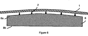
図2〜7に示されるように、この問題は、凸状の前面8aを有するマイクロドット2の支持基板8を用いることによって解決される。そのとき、全てのマイクロドット2の自由端は、実際には、記憶媒体1の感応領域に接触した状態になり、その可撓性は、少なくともマイクロドットの高さの変化の大部分を吸収するのに十分である。基板8の前面8aのキャンバーは、極めて小さいままであるが、装置を組み立てる間又は熱的ドリフトに起因して反対方向に発生する傾向がある変形を考慮するのに十分である。実際には、凸状の面の曲線半径は、1m〜5mの間に含まれても良い。好ましくは、約10nm〜100μmのキャンバーに対応して約2mである。
As shown in FIGS. 2 to 7, this problem is solved by using a
そのような基板8の前面のキャンバーは、とりわけ、マイクロドットの形成前の前面8aの化学的機械研磨(CMP)によって得られる。この場合には、図2〜4及び6に図示されるように、基板8の背面8bは、ほぼ平坦のままである。
Such a camber on the front surface of the
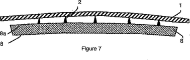
前面8aのキャンバーは、基板8上の機械的応力を適用することによっても得られる。この機械的応力は、例えば、前面8a上に圧縮的に圧迫される薄い層(図示されていない)の堆積又は背面8b上に伸張的に圧迫される薄い層(図示されていない)の堆積によって達成される。いずれの場合にも、そのような機械的に圧縮的又は伸張的に圧迫される薄い層を適用することは、図7に示されるように、基板8の前面8a及び背面8bのほぼ平行な変形を引き起こす。特定の実施例では、薄い層は、圧迫されるシリコン窒化薄膜の層又はいかなる不利な効果もなく1GPaの応力を支持することができる数百nmの厚さを有する圧迫されるシリコンの層である。
The camber of the
圧迫される層は、とりわけ、イオンビームスパッタリング(IBS)堆積によって得られる。原型基板と呼ばれる別の基板によって予め圧迫され、任意の適切な移動技術、例えば、原型基板の接着及び薄型化によって上反りされる基板8に対して移動されても良い。基板8の厚さは、キャンバリングステップを促すように有利に選択されても良い。例えば、基板8は、例えば約100μmに低減される厚さを有しても良い。
The layer to be pressed is obtained, inter alia, by ion beam sputtering (IBS) deposition. It may be moved against the
記憶媒体の感応領域が十分な可撓性であるときには、マイクロドット2は、アドレッシング回路及び制御回路が集積されても良好なベース基板8上に、カンチレバーなしに直接形成されても良い。
When the sensitive area of the storage medium is sufficiently flexible, the
上記に示されるように、薄膜4を含む記憶媒体1の感応領域の可撓性は、マイクロドット2と感応領域の間のコンタクトを確保し、マイクロドットの高さの変化のほとんどを吸収するために、凸状の面の基板と協同する。マイクロドット2を支持する前面8aが凸状である基板8と図1〜5に係る記憶媒体の組み合わせは、全てのマイクロドット間の組立力の良好な再分配を保証する。実際には、組み立てが行われるときには、その平面内の感応領域の移動の自由度を失わない間に、外部フレーム3は、基板8に安全に取り付けられても良い。外部基板3は、とりわけ、ボンディング、熱溶融又は壁の間の接着を達成するための任意の他の方法のような従来の方法によって、基板8に固定されても良い。そのとき、組立力は、記憶媒体、とりわけ、マイクロドット2のアレイ上に可撓性薄膜4を含むその感応領域を圧迫する。各マイクロドット2によって加えられる基本的な力は約0.1nN〜10nNであっても良い。曲線半径の関数が選択される。例えば、そのとき、組立力は、1mNより大きくても良い。
As indicated above, the flexibility of the sensitive area of the
データ記録装置は、一般的には、記憶媒体1の感応領域及び感応領域のほぼ水平な面内のマイクロドット2の相対的な移動を可能にする手段(とりわけ、アクチュエータ7)を含む。マイクロドットを感応領域に接触させるためのマイクロドットの支持基板8に対してほぼ垂直(すなわち、縦横)方向への移動手段を含んでも良い。
The data recording device generally includes a sensitive area of the
例えば、図1に示された異なる素子の各寸法は以下の通りである。
−記憶媒体1の寸法c1は約15mm
−薄膜4の寸法c2は約9.5mm
−内部フレーム5の幅l1は約0.25mm
−外部フレーム3の幅l2は約0.5mm
−固定薄膜6の幅l3は約2mm
For example, the dimensions of the different elements shown in FIG. 1 are as follows.
The dimension c1 of the
-The dimension c2 of the
-The width l1 of the
-The width l2 of the
-The width 13 of the fixed
Claims (11)
前記基板(8)上に配置されるナノメータ規模のマイクロドット(2)の2次元アレイと、
前記マイクロドット(2)に面する記憶層(9)と、
前記記憶層(9)を覆う可撓性薄膜(4)と、
前記可撓性薄膜(4)を外部フレーム(3)上へ固定し、且つ、前記基板(8)に沿った面で前記可撓性薄膜(4)の移動を可能にする可撓性固定手段を備え、
前記可撓性固定手段は、前記可撓性薄膜(4)の周辺に広がる固定薄膜(6)によって形成され、且つ、前記基板(8)に対して垂直に前記可撓性薄膜(4)の移動を可能にする、ことを特徴とするデータ記録装置。A substrate (8);
A two-dimensional array of nanometer-scale microdots (2) disposed on the substrate (8) ;
A storage layer (9) facing the microdot (2);
A flexible thin film (4) covering the storage layer (9) ;
Flexible fixing means for fixing the flexible thin film (4) onto the outer frame (3) and allowing the flexible thin film (4) to move on a surface along the substrate (8). With
The flexible fixing means is formed by a fixed thin film (6) spreading around the flexible thin film (4), and the flexible thin film (4) is perpendicular to the substrate (8) . to allow movement, the data recording apparatus characterized by.
Applications Claiming Priority (3)
| Application Number | Priority Date | Filing Date | Title |
|---|---|---|---|
| FR0500471 | 2005-01-17 | ||
| FR0500471A FR2880979B1 (en) | 2005-01-17 | 2005-01-17 | DATA RECORDING DEVICE HAVING A PERIPHERAL SUPPORT MEMBRANE AND METHOD FOR MANUFACTURING THE SAME |
| PCT/FR2005/003261 WO2006075066A1 (en) | 2005-01-17 | 2005-12-22 | Device for recording data, comprising a peripheral support membrane, and method for producing the same |
Publications (2)
| Publication Number | Publication Date |
|---|---|
| JP2008527606A JP2008527606A (en) | 2008-07-24 |
| JP4898705B2 true JP4898705B2 (en) | 2012-03-21 |
Family
ID=34954845
Family Applications (1)
| Application Number | Title | Priority Date | Filing Date |
|---|---|---|---|
| JP2007550812A Expired - Fee Related JP4898705B2 (en) | 2005-01-17 | 2005-12-22 | Data recording apparatus including peripheral supporting thin film and method of manufacturing the apparatus |
Country Status (5)
| Country | Link |
|---|---|
| US (1) | US7898931B2 (en) |
| EP (1) | EP1839304A1 (en) |
| JP (1) | JP4898705B2 (en) |
| FR (1) | FR2880979B1 (en) |
| WO (1) | WO2006075066A1 (en) |
Families Citing this family (1)
| Publication number | Priority date | Publication date | Assignee | Title |
|---|---|---|---|---|
| US9221678B2 (en) * | 2008-10-06 | 2015-12-29 | University Of Florida Research Foundation, Inc. | Active fixturing for micro/mesoscale, machine tool systems |
Citations (2)
| Publication number | Priority date | Publication date | Assignee | Title |
|---|---|---|---|---|
| JPH1040597A (en) * | 1996-07-25 | 1998-02-13 | Tdk Corp | Memory apparatus |
| JP2000152596A (en) * | 1998-10-30 | 2000-05-30 | Internatl Business Mach Corp <Ibm> | Magnetic scanning/positioning system with at least two items of degree of freedom |
Family Cites Families (10)
| Publication number | Priority date | Publication date | Assignee | Title |
|---|---|---|---|---|
| US5216631A (en) * | 1990-11-02 | 1993-06-01 | Sliwa Jr John W | Microvibratory memory device |
| FR2757992B1 (en) * | 1996-12-26 | 1999-01-29 | Commissariat Energie Atomique | INFORMATION RECORDING MEDIUM, DEVICE FOR READING THE MEDIA, AND METHODS OF IMPLEMENTING THE DEVICE |
| DE60117719T2 (en) * | 2000-06-26 | 2006-11-16 | Samsung Electronics Co., Ltd. | Electromagnetic X-Y positioning system for nanodata storage system and method of making coils for same |
| JP2002092946A (en) * | 2000-09-20 | 2002-03-29 | Toshiba Corp | Optical disk substrate and method of manufacturing the same |
| US6522566B2 (en) * | 2000-12-01 | 2003-02-18 | Hewlett-Packard Company | System modules with atomic resolution storage memory |
| US7018572B2 (en) * | 2001-06-11 | 2006-03-28 | General Electric Company | Method for producing data storage media |
| FR2845513B1 (en) * | 2002-10-03 | 2006-08-11 | Commissariat Energie Atomique | DATA RECORDING DEVICE HAVING MEMBRANE MEMORY MEMORY MEDIUM |
| JP2005004921A (en) * | 2003-06-13 | 2005-01-06 | Alps Electric Co Ltd | Highly precise positioning device |
| FR2856184B1 (en) | 2003-06-13 | 2008-04-11 | Commissariat Energie Atomique | DATA RECORDING DEVICE COMPRISING MICROPOINT AND RECORDING MEDIUM |
| DE602004017732D1 (en) | 2003-07-03 | 2008-12-24 | Commissariat Energie Atomique | METHOD FOR RECORDING DATA AND DEVICE FOR CARRYING OUT THE PROCESS WITH DEFORMABLE MEMORY CARRIER |
-
2005
- 2005-01-17 FR FR0500471A patent/FR2880979B1/en not_active Expired - Fee Related
- 2005-12-22 EP EP05850600A patent/EP1839304A1/en not_active Withdrawn
- 2005-12-22 JP JP2007550812A patent/JP4898705B2/en not_active Expired - Fee Related
- 2005-12-22 WO PCT/FR2005/003261 patent/WO2006075066A1/en not_active Ceased
- 2005-12-22 US US11/794,007 patent/US7898931B2/en not_active Expired - Fee Related
Patent Citations (2)
| Publication number | Priority date | Publication date | Assignee | Title |
|---|---|---|---|---|
| JPH1040597A (en) * | 1996-07-25 | 1998-02-13 | Tdk Corp | Memory apparatus |
| JP2000152596A (en) * | 1998-10-30 | 2000-05-30 | Internatl Business Mach Corp <Ibm> | Magnetic scanning/positioning system with at least two items of degree of freedom |
Also Published As
| Publication number | Publication date |
|---|---|
| FR2880979A1 (en) | 2006-07-21 |
| US7898931B2 (en) | 2011-03-01 |
| JP2008527606A (en) | 2008-07-24 |
| WO2006075066A1 (en) | 2006-07-20 |
| EP1839304A1 (en) | 2007-10-03 |
| FR2880979B1 (en) | 2007-03-16 |
| US20080095021A1 (en) | 2008-04-24 |
Similar Documents
| Publication | Publication Date | Title |
|---|---|---|
| US7570416B2 (en) | Method and apparatus for a reflective spatial light modulator with a flexible pedestal | |
| US7245358B2 (en) | Substrate support system | |
| JP2013538446A (en) | Formation of devices with curved piezoelectric films | |
| US7101272B2 (en) | Carrier head for thermal drift compensation | |
| JP2001060618A (en) | Substrate suction holding method, substrate suction holding apparatus, exposure apparatus using the substrate suction holding apparatus, and device manufacturing method | |
| CN101297227A (en) | High fill ratio silicon spatial light modulator | |
| JP4898705B2 (en) | Data recording apparatus including peripheral supporting thin film and method of manufacturing the apparatus | |
| JPH08241835A (en) | Recording medium of semiconductor layer structure and large capacity memory device | |
| US20130001719A1 (en) | Interaction structure for a storage medium | |
| JP4494337B2 (en) | Data recording apparatus having diaphragm type support | |
| JP2008527605A (en) | Data recording apparatus having microdots having free ends forming a convex surface and method of manufacturing the apparatus | |
| CN109411359A (en) | Method and apparatus for handling semiconductor device structure | |
| US8334967B2 (en) | Substrate support system having a plurality of contact lands | |
| JP2006502523A5 (en) | ||
| JP5044384B2 (en) | Optical element and optical functional element | |
| JP4353337B2 (en) | Information storage device using probe | |
| JP2013049112A (en) | Polishing pad and manufacturing method thereof | |
| CN117642844A (en) | Method for adjusting wafer shape using multi-directional actuation film | |
| JP3699950B2 (en) | Wafer polisher |
Legal Events
| Date | Code | Title | Description |
|---|---|---|---|
| A621 | Written request for application examination |
Free format text: JAPANESE INTERMEDIATE CODE: A621 Effective date: 20081201 |
|
| A977 | Report on retrieval |
Free format text: JAPANESE INTERMEDIATE CODE: A971007 Effective date: 20101007 |
|
| A131 | Notification of reasons for refusal |
Free format text: JAPANESE INTERMEDIATE CODE: A131 Effective date: 20101015 |
|
| A521 | Request for written amendment filed |
Free format text: JAPANESE INTERMEDIATE CODE: A523 Effective date: 20110114 |
|
| A131 | Notification of reasons for refusal |
Free format text: JAPANESE INTERMEDIATE CODE: A131 Effective date: 20110527 |
|
| A521 | Request for written amendment filed |
Free format text: JAPANESE INTERMEDIATE CODE: A523 Effective date: 20110823 |
|
| TRDD | Decision of grant or rejection written | ||
| A01 | Written decision to grant a patent or to grant a registration (utility model) |
Free format text: JAPANESE INTERMEDIATE CODE: A01 Effective date: 20111129 |
|
| A01 | Written decision to grant a patent or to grant a registration (utility model) |
Free format text: JAPANESE INTERMEDIATE CODE: A01 |
|
| A61 | First payment of annual fees (during grant procedure) |
Free format text: JAPANESE INTERMEDIATE CODE: A61 Effective date: 20111226 |
|
| R150 | Certificate of patent or registration of utility model |
Free format text: JAPANESE INTERMEDIATE CODE: R150 |
|
| FPAY | Renewal fee payment (event date is renewal date of database) |
Free format text: PAYMENT UNTIL: 20150106 Year of fee payment: 3 |
|
| LAPS | Cancellation because of no payment of annual fees |