JP4494337B2 - Data recording apparatus having diaphragm type support - Google Patents
Data recording apparatus having diaphragm type support Download PDFInfo
- Publication number
- JP4494337B2 JP4494337B2 JP2005500037A JP2005500037A JP4494337B2 JP 4494337 B2 JP4494337 B2 JP 4494337B2 JP 2005500037 A JP2005500037 A JP 2005500037A JP 2005500037 A JP2005500037 A JP 2005500037A JP 4494337 B2 JP4494337 B2 JP 4494337B2
- Authority
- JP
- Japan
- Prior art keywords
- diaphragm
- array
- layer
- frame
- storage medium
- Prior art date
- Legal status (The legal status is an assumption and is not a legal conclusion. Google has not performed a legal analysis and makes no representation as to the accuracy of the status listed.)
- Expired - Fee Related
Links
- 238000003860 storage Methods 0.000 claims description 43
- XUIMIQQOPSSXEZ-UHFFFAOYSA-N Silicon Chemical compound [Si] XUIMIQQOPSSXEZ-UHFFFAOYSA-N 0.000 claims description 28
- 229910052710 silicon Inorganic materials 0.000 claims description 27
- 239000010703 silicon Substances 0.000 claims description 27
- 125000006850 spacer group Chemical group 0.000 claims description 27
- 238000003491 array Methods 0.000 claims description 10
- OKTJSMMVPCPJKN-UHFFFAOYSA-N Carbon Chemical compound [C] OKTJSMMVPCPJKN-UHFFFAOYSA-N 0.000 claims description 9
- 229910052799 carbon Inorganic materials 0.000 claims description 9
- 230000006870 function Effects 0.000 claims description 7
- VYPSYNLAJGMNEJ-UHFFFAOYSA-N Silicium dioxide Chemical compound O=[Si]=O VYPSYNLAJGMNEJ-UHFFFAOYSA-N 0.000 claims description 5
- 230000015572 biosynthetic process Effects 0.000 claims description 3
- ZOXJGFHDIHLPTG-UHFFFAOYSA-N Boron Chemical compound [B] ZOXJGFHDIHLPTG-UHFFFAOYSA-N 0.000 claims description 2
- 229910052581 Si3N4 Inorganic materials 0.000 claims description 2
- 229910003481 amorphous carbon Inorganic materials 0.000 claims description 2
- 229910052796 boron Inorganic materials 0.000 claims description 2
- 239000000377 silicon dioxide Substances 0.000 claims description 2
- 235000012239 silicon dioxide Nutrition 0.000 claims description 2
- HQVNEWCFYHHQES-UHFFFAOYSA-N silicon nitride Chemical compound N12[Si]34N5[Si]62N3[Si]51N64 HQVNEWCFYHHQES-UHFFFAOYSA-N 0.000 claims description 2
- 229910052709 silver Inorganic materials 0.000 claims description 2
- 239000004332 silver Substances 0.000 claims description 2
- 239000010410 layer Substances 0.000 description 58
- 238000000034 method Methods 0.000 description 15
- 230000000694 effects Effects 0.000 description 11
- 238000004519 manufacturing process Methods 0.000 description 10
- 238000005516 engineering process Methods 0.000 description 9
- 238000005530 etching Methods 0.000 description 7
- 239000012782 phase change material Substances 0.000 description 4
- 238000013500 data storage Methods 0.000 description 3
- 238000011161 development Methods 0.000 description 3
- 239000000463 material Substances 0.000 description 3
- 238000004377 microelectronic Methods 0.000 description 3
- 239000000523 sample Substances 0.000 description 3
- 238000003486 chemical etching Methods 0.000 description 2
- 238000005229 chemical vapour deposition Methods 0.000 description 2
- 239000010432 diamond Substances 0.000 description 2
- 230000006386 memory function Effects 0.000 description 2
- 238000005240 physical vapour deposition Methods 0.000 description 2
- 230000008569 process Effects 0.000 description 2
- 239000011347 resin Substances 0.000 description 2
- 229920005989 resin Polymers 0.000 description 2
- KWYUFKZDYYNOTN-UHFFFAOYSA-M Potassium hydroxide Chemical compound [OH-].[K+] KWYUFKZDYYNOTN-UHFFFAOYSA-M 0.000 description 1
- 229910004298 SiO 2 Inorganic materials 0.000 description 1
- NRTOMJZYCJJWKI-UHFFFAOYSA-N Titanium nitride Chemical compound [Ti]#N NRTOMJZYCJJWKI-UHFFFAOYSA-N 0.000 description 1
- 230000009471 action Effects 0.000 description 1
- 230000002411 adverse Effects 0.000 description 1
- 239000002775 capsule Substances 0.000 description 1
- 230000000295 complement effect Effects 0.000 description 1
- 239000013078 crystal Substances 0.000 description 1
- 238000005520 cutting process Methods 0.000 description 1
- 230000007423 decrease Effects 0.000 description 1
- 238000013461 design Methods 0.000 description 1
- 229910003460 diamond Inorganic materials 0.000 description 1
- 230000001747 exhibiting effect Effects 0.000 description 1
- 239000000696 magnetic material Substances 0.000 description 1
- 229910052751 metal Inorganic materials 0.000 description 1
- 239000002184 metal Substances 0.000 description 1
- 238000000386 microscopy Methods 0.000 description 1
- 230000003287 optical effect Effects 0.000 description 1
- 238000004806 packaging method and process Methods 0.000 description 1
- 238000000059 patterning Methods 0.000 description 1
- 229920002120 photoresistant polymer Polymers 0.000 description 1
- 239000004033 plastic Substances 0.000 description 1
- 238000012545 processing Methods 0.000 description 1
- 238000011160 research Methods 0.000 description 1
- 238000004621 scanning probe microscopy Methods 0.000 description 1
- 229910052814 silicon oxide Inorganic materials 0.000 description 1
- 239000002356 single layer Substances 0.000 description 1
- 239000007787 solid Substances 0.000 description 1
- 239000000126 substance Substances 0.000 description 1
- 238000001931 thermography Methods 0.000 description 1
- 239000012815 thermoplastic material Substances 0.000 description 1
- UONOETXJSWQNOL-UHFFFAOYSA-N tungsten carbide Chemical compound [W+]#[C-] UONOETXJSWQNOL-UHFFFAOYSA-N 0.000 description 1
- 235000012431 wafers Nutrition 0.000 description 1
Images


Classifications
-
- B—PERFORMING OPERATIONS; TRANSPORTING
- B82—NANOTECHNOLOGY
- B82Y—SPECIFIC USES OR APPLICATIONS OF NANOSTRUCTURES; MEASUREMENT OR ANALYSIS OF NANOSTRUCTURES; MANUFACTURE OR TREATMENT OF NANOSTRUCTURES
- B82Y10/00—Nanotechnology for information processing, storage or transmission, e.g. quantum computing or single electron logic
-
- G—PHYSICS
- G11—INFORMATION STORAGE
- G11B—INFORMATION STORAGE BASED ON RELATIVE MOVEMENT BETWEEN RECORD CARRIER AND TRANSDUCER
- G11B9/00—Recording or reproducing using a method not covered by one of the main groups G11B3/00 - G11B7/00; Record carriers therefor
- G11B9/12—Recording or reproducing using a method not covered by one of the main groups G11B3/00 - G11B7/00; Record carriers therefor using near-field interactions; Record carriers therefor
- G11B9/14—Recording or reproducing using a method not covered by one of the main groups G11B3/00 - G11B7/00; Record carriers therefor using near-field interactions; Record carriers therefor using microscopic probe means, i.e. recording or reproducing by means directly associated with the tip of a microscopic electrical probe as used in Scanning Tunneling Microscopy [STM] or Atomic Force Microscopy [AFM] for inducing physical or electrical perturbations in a recording medium; Record carriers or media specially adapted for such transducing of information
-
- G—PHYSICS
- G11—INFORMATION STORAGE
- G11B—INFORMATION STORAGE BASED ON RELATIVE MOVEMENT BETWEEN RECORD CARRIER AND TRANSDUCER
- G11B23/00—Record carriers not specific to the method of recording or reproducing; Accessories, e.g. containers, specially adapted for co-operation with the recording or reproducing apparatus ; Intermediate mediums; Apparatus or processes specially adapted for their manufacture
- G11B23/0014—Record carriers not specific to the method of recording or reproducing; Accessories, e.g. containers, specially adapted for co-operation with the recording or reproducing apparatus ; Intermediate mediums; Apparatus or processes specially adapted for their manufacture record carriers not specifically of filamentary or web form
-
- G—PHYSICS
- G11—INFORMATION STORAGE
- G11B—INFORMATION STORAGE BASED ON RELATIVE MOVEMENT BETWEEN RECORD CARRIER AND TRANSDUCER
- G11B9/00—Recording or reproducing using a method not covered by one of the main groups G11B3/00 - G11B7/00; Record carriers therefor
- G11B9/12—Recording or reproducing using a method not covered by one of the main groups G11B3/00 - G11B7/00; Record carriers therefor using near-field interactions; Record carriers therefor
- G11B9/14—Recording or reproducing using a method not covered by one of the main groups G11B3/00 - G11B7/00; Record carriers therefor using near-field interactions; Record carriers therefor using microscopic probe means, i.e. recording or reproducing by means directly associated with the tip of a microscopic electrical probe as used in Scanning Tunneling Microscopy [STM] or Atomic Force Microscopy [AFM] for inducing physical or electrical perturbations in a recording medium; Record carriers or media specially adapted for such transducing of information
- G11B9/1418—Disposition or mounting of heads or record carriers
-
- G—PHYSICS
- G11—INFORMATION STORAGE
- G11B—INFORMATION STORAGE BASED ON RELATIVE MOVEMENT BETWEEN RECORD CARRIER AND TRANSDUCER
- G11B9/00—Recording or reproducing using a method not covered by one of the main groups G11B3/00 - G11B7/00; Record carriers therefor
- G11B9/12—Recording or reproducing using a method not covered by one of the main groups G11B3/00 - G11B7/00; Record carriers therefor using near-field interactions; Record carriers therefor
- G11B9/14—Recording or reproducing using a method not covered by one of the main groups G11B3/00 - G11B7/00; Record carriers therefor using near-field interactions; Record carriers therefor using microscopic probe means, i.e. recording or reproducing by means directly associated with the tip of a microscopic electrical probe as used in Scanning Tunneling Microscopy [STM] or Atomic Force Microscopy [AFM] for inducing physical or electrical perturbations in a recording medium; Record carriers or media specially adapted for such transducing of information
- G11B9/1463—Record carriers for recording or reproduction involving the use of microscopic probe means
- G11B9/1472—Record carriers for recording or reproduction involving the use of microscopic probe means characterised by the form
-
- G—PHYSICS
- G11—INFORMATION STORAGE
- G11B—INFORMATION STORAGE BASED ON RELATIVE MOVEMENT BETWEEN RECORD CARRIER AND TRANSDUCER
- G11B17/00—Guiding record carriers not specifically of filamentary or web form, or of supports therefor
- G11B17/32—Maintaining desired spacing between record carrier and head, e.g. by fluid-dynamic spacing
-
- G—PHYSICS
- G11—INFORMATION STORAGE
- G11B—INFORMATION STORAGE BASED ON RELATIVE MOVEMENT BETWEEN RECORD CARRIER AND TRANSDUCER
- G11B5/00—Recording by magnetisation or demagnetisation of a record carrier; Reproducing by magnetic means; Record carriers therefor
- G11B2005/0002—Special dispositions or recording techniques
- G11B2005/0005—Arrangements, methods or circuits
Description
〔発明の背景〕
本発明は、記憶媒体に向いた平面内に配置されていて頂点がナノメートル台の寸法のものであるマイクロティップ(Microtip)の2次元アレイ及び記憶媒体上へのデータの記録を可能にするようマイクロティップをアドレス指定してこれを制御する電子的手段を有するデータ記録装置に関する。
BACKGROUND OF THE INVENTION
The present invention enables a two-dimensional array of microtips arranged in a plane facing the storage medium and having apexes on the order of nanometers and the recording of data on the storage medium. The present invention relates to a data recording apparatus having electronic means for addressing and controlling microtips.
〔技術の現状〕
コンピュータ分野とマルチメディア分野の両方におけるデータ記録は、容量に関する要望の高まりに応えなければならない。光学素子及び相変化材料を用いて磁気ハードディスクからDVDまでの範囲にわたる種々の技術が開発された。用いられる記録技術が何であれ、メモリポイント(ビット)のサイズを減少させ、記憶密度を増大させる記録容量手段を増加させることが求められていることに変わりはない。
[Current state of technology]
Data recording in both the computer and multimedia fields must meet the growing demand for capacity. Various technologies ranging from magnetic hard disks to DVDs have been developed using optical elements and phase change materials. Whatever the recording technique used, there is still a need to increase the recording capacity means to reduce the size of memory points (bits) and increase the storage density.
最近、ティップ効果型顕微鏡で用いられる形式のマイクロティップを実現することにより約1テラビット/cm2の極めて大きな記憶容量が得られた(2000年5月発行のP.ベチガー(P. Vettiger)他著,「1000の足−将来のAFMデータ記憶用の1000以上のティップ(The Millipede-More than one thousand tips for future AFM data storage)」,アイビーエム・ジャーナル・リサーチ・ディベロップメント(IBM J. RES. Develop.),第44巻,第3号,P323〜340及び2001年発行のドンウェオン・リー(Dong-Weon Lee)他著,「ナノメートル台の熱的画像取得およびデータ記憶用サブ100nmナノヒータのマイクロプローブアレイの製造(Fabrication of microprobe array with sub-100nm nano-heater for nanometric thermal imaging and data storage)」,テクニカル・ダイジェスト(Technical Digest),メムス2001(MEMS 2001 ),第14回・IEEE・インターナショナル・カンフェレンス・オン・マイクロ・エレクトロ・メカニカル・システムズ(14th IEEE International Conference on Micro Electro Mechanical Systems)(Cat. N°01CH37090 )PIEEEPピスカッタウェイ,ニュージャージー州,米国,P204〜207)。高密度は、マイクロティップによりビットを局所化することにより得られ、マイクロティップの頂点は、ナノメートル台の寸法のものである。マイクロティップは好ましくは、データに対して並列アクセス方式でアレイ状に配列され、それにより速度に関する限り優れた性能を達成することができる。単一のアクチュエータ(これは、電気機械的なものであるのがよい)により、記憶媒体の表面に対するマイクロティップのアレイ全体の相対的一体運動が可能になる。 Recently, an extremely large memory capacity of about 1 terabit / cm 2 was obtained by realizing a microtip of the type used in the tip effect microscope (P. Vettiger, published in May 2000) , "The Millipede-More than one thousand tips for future AFM data storage", IBM Journal Research Development (IBM J. RES. Develop. , Vol. 44, No. 3, P323-340 and Dong-Weon Lee et al., 2001, “Microprobe array of sub-100 nm nanoheaters for nanometer thermal image acquisition and data storage. "Fabrication of microprobe array with sub-100nm nano-heater for nanometric thermal imaging and data storage" Esuto (Technical Digest), MEMS 2001 (MEMS 2001), 14th, IEEE, International Conference On Micro Electro Mechanical Systems (14 th IEEE International Conference on Micro Electro Mechanical Systems) (Cat. N ° 01CH37090 ) PIEEEEP Piscataway, New Jersey, USA, P204-207). High density is obtained by localizing the bits with microtips, where the tops of the microtips are of the order of nanometers. The microtips are preferably arranged in an array in a parallel access manner with respect to the data so that excellent performance can be achieved as far as speed is concerned. A single actuator (which may be electromechanical) allows relative integral movement of the entire array of microtips relative to the surface of the storage medium.
かかるティップ効果方式のデータ記録装置では、全てのティップと記憶媒体を完全に接触させることが必要である。システムの複雑さのために、各マイクロティップの位置を個々に制御することは期待できない。しかしながら、マイクロティップは、マイクロエレクトロニクスの技術に由来する技術によってひとまとめに製作され、マイクロティップの高さのばらつきは、製作に起因して常に存在したままである。このばらつきは非常に小さく、典型的には約100nmであるが、アレイを構成するマイクロティップのうち最も長いものが、他のマイクロティップよりも一層強く記憶媒体に押し当たる。 In such a tip effect type data recording apparatus, it is necessary to completely contact all the tips with the storage medium. Due to the complexity of the system, it is not possible to control the position of each microtip individually. However, the microtips are manufactured together by a technique derived from the technology of microelectronics, and variations in the height of the microtips always exist due to the manufacturing. This variation is very small, typically about 100 nm, but the longest of the microtips that make up the array presses against the storage medium more strongly than the other microtips.
この問題を解決するため、各マイクロティップは、局所プローブ顕微鏡で用いられるマイクロティップアレイと類似したやり方でカンチレバーの一端部によりオーバーハングした状態で支持される。この場合、カンチレバーの可撓性により、支承体の歪みを吸収することができる。 To solve this problem, each microtip is supported overhang by one end of the cantilever in a manner similar to the microtip array used in a local probe microscope. In this case, distortion of the support body can be absorbed by the flexibility of the cantilever.
しかしながら、記憶媒体に加わるマイクロティップの支承力は、記憶媒体を損傷させないよう約100nNの値を超えてはならない。さらに言えば、記憶媒体とのマイクロティップの接触面が微小なので、圧力が高い。したがって、カンチレバーは、マイクロティップの高さのばらつきを吸収するよう可撓性が非常に高くなければならない。例えば、剛性が約1N/m、長さが約100μm、幅が数十μm、厚さが数μmのカンチレバーが開発された。これ以上可撓性の高いカンチレバーを計画することは困難である。これらの寸法形状は事実、これらの小さな幅及び(又は)高さと比較して長さが大きいので使いこなすのが困難である。加うるに、記憶媒体の表面に向いたティップの位置決め精度に悪影響が生じ、かくして記憶密度が制限される。 However, the microtip bearing force applied to the storage medium should not exceed a value of about 100 nN so as not to damage the storage medium. Furthermore, since the contact surface of the microtip with the storage medium is minute, the pressure is high. Therefore, the cantilever must be very flexible to absorb the microtip height variations. For example, a cantilever having a rigidity of about 1 N / m, a length of about 100 μm, a width of several tens of μm, and a thickness of several μm has been developed. It is difficult to plan a more flexible cantilever. These dimensions are in fact difficult to master because of their large length compared to their small width and / or height. In addition, the positioning accuracy of the tip facing the surface of the storage medium is adversely affected, thus limiting the storage density.
〔発明の目的〕
本発明の目的は、上述の欠点がなく、特にマイクロティップの高さ方向のばらつきを無視できるようにするデータ記録装置を提供することにある。
(Object of invention)
An object of the present invention is to provide a data recording apparatus that does not have the above-mentioned drawbacks and that can particularly ignore variations in the height direction of microtips.
本発明によれば、この目的は、記憶媒体が複数のセルを形成するフレームによって支持された可撓性ダイヤフラムを有し、少なくとも1つのマイクロティップが各セルと関連していることによって達成される。このフレームにより、ダイヤフラムの剛性を確保でき、しかも各セル内部でのその運動の自由度を確保することができる。 According to the invention, this object is achieved by the fact that the storage medium has a flexible diaphragm supported by a frame forming a plurality of cells, at least one microtip being associated with each cell. . With this frame, the rigidity of the diaphragm can be secured, and the freedom of movement within each cell can be secured.
本発明の開発例によれば、マイクロティップの2つのアレイは、記憶媒体の各側に設けられる。 According to a development of the invention, two arrays of microtips are provided on each side of the storage medium.
マイクロティップの2つのアレイは好ましくは、フレームのいずれか1つのセルと関連したマイクロティップが互いに正確に対向して配置されることはないように側方にずらされる。 The two arrays of microtips are preferably offset laterally so that the microtips associated with any one cell of the frame are not placed exactly opposite each other.
好ましい実施形態によれば、可撓性ダイヤフラムは少なくとも、メモリの機能を実行する第1の層及び或る程度の剛性を確保するよう設計された第2の層を有する。 According to a preferred embodiment, the flexible diaphragm has at least a first layer that performs the function of the memory and a second layer that is designed to ensure some degree of rigidity.
本発明の別の開発例によれば、可撓性ダイヤフラムは、フレームに対し側方にずらされたスペーサ要素のアレイによって分離された第1の基本ダイヤフラム及び第2の基本ダイヤフラムから成る。これにより、望ましくないエッジ効果を無くすことができる。 According to another development of the invention, the flexible diaphragm consists of a first basic diaphragm and a second basic diaphragm separated by an array of spacer elements offset laterally with respect to the frame. Thereby, an undesirable edge effect can be eliminated.
これ又エッジ効果を制限することができる別の変形実施形態では、データ記録装置は、スペーサスタッドの2次元アレイによってダイヤフラムから分離されていて、各セルを各々が少なくとも1つのマイクロティップと関連した複数の基本セルに細分する可撓性プレートのアレイを有する。 In another alternative embodiment that can also limit edge effects, the data recording device is separated from the diaphragm by a two-dimensional array of spacer studs, each cell being associated with at least one microtip. With an array of flexible plates subdivided into basic cells.
データ記録装置は好ましくは、上述の平面に平行に、場合によってはこれに垂直に記憶媒体とマイクロティップアレイの相対運動を可能にする手段を有する。 The data recording device preferably comprises means for allowing relative movement of the storage medium and the microtip array parallel to the plane described above and possibly perpendicular thereto.
他の利点及び特徴は、非限定的な例として与えられているに過ぎず、添付の図面に記載された本発明の特定の実施形態についての詳細な説明から明らかになろう。 Other advantages and features are provided by way of non-limiting example only and will be apparent from the detailed description of specific embodiments of the invention as set forth in the accompanying drawings.
〔特定の実施形態の説明〕
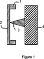
図1に示すように、データ記録装置の基本要素は、フレーム1を含み、このフレーム1は、そのフェースのうちの一方に、記憶媒体を構成するフレキシブル又は可撓性ダイヤフラム2を支持している。各基本要素は、マイクロティップ3と関連したセルを形成しており、このマイクロティップ3は、記憶媒体に平行に記憶媒体に向いた状態で配置されたベース4上に形成されている。
[Description of Specific Embodiments]
As shown in FIG. 1, the basic element of the data recording apparatus includes a
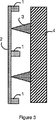
データ記録装置は、マイクロティップの2次元アレイ(図3〜図5)と関連した複数の隣り合うセルを有する。図4及び図5は、用いることができる2つの特定の形態を示しており、セルの形状はそれぞれ、矩形(図2及び図4)及び6角形(図5)である。 The data recording device has a plurality of adjacent cells associated with a two-dimensional array of microtips (FIGS. 3-5). 4 and 5 show two specific configurations that can be used, the cell shape being rectangular (FIGS. 2 and 4) and hexagon (FIG. 5), respectively.
休止位置では、マイクロティップ3は、可撓性ダイヤフラム2と接触状態にあるか又は可撓性ダイヤフラムに対して引っ込められているかのいずれかであるのがよい。後者の場合、読取り又は書き込み位置では、記憶媒体をベース4に垂直に動かしてマイクロティップ3を可撓性ダイヤフラム2によって形成された記憶媒体に接触させる。記憶媒体とマイクロティップのこれら平面に垂直な相対運動は好ましくは、ダイヤフラムの支持フレーム1の運動によって達成され、マイクロティップ3は、ベース4上に固定されたままの状態で形成される。
In the rest position, the
可撓性ダイヤフラムと接触しているかどうかにかかわらず、可撓性ダイヤフラムの平面に平行な方向におけるマイクロティップ3と記憶媒体の相対運動は又、それ自体マイクロコンピュータにより制御されるアクチュエータ(図示せず)によりダイヤフラム及び(又は)マイクロティップに伝達できる。
Regardless of whether it is in contact with the flexible diaphragm, the relative movement of the
読取り又は書き込み位置でのマイクロティップ3の制御及びアドレス指定又は多重化は、任意適当な手段、好ましくは、ベース4内に設けられた集積技術によって達成される電子回路により行われる。この場合、固定状態のマイクロティップ3は、シリコンに搭載されるマイクロエレクトロニクス技術によって達成できる。記憶媒体に向いた状態で配置されるベース4の表面全体は実際に、多くの先行技術の装置の場合とは異なり、記憶を目的として取り外す必要はないマイクロティップの電子アドレス指定及び制御回路に利用できる。これにより、用いられるシリコン表面を最適化することができる。電気的メモリの場合、電流は、マイクロティップから導電性ダイヤフラムに流れなければならず、このダイヤフラムはこの場合、電気的接続部(図示せず)によってベース4内に設けられた電子回路に接続される。
Control and addressing or multiplexing of the
可撓性ダイヤフラム2は、厚さが極めて小さく、即ち、約数ナノメートルから数マイクロメートルであり、導電性であるのがよい層によって形成される。したがって、可撓性ダイヤフラムは、その表面に垂直な局所的力の作用を受けて変形する。例えば、100nNの一点集中力の作用を受けた場合、約100μmの寸法(辺、直径等)のフレームにぴんと張った状態で被着された厚さ10nmのダイヤモンド様炭素層は、変形して約12μmのたるみを生じるが、これは、ほんの8.3nN/μmの等価剛性に相当し、即ち、従来型カンチレバーのたるみの1/100以下である。これよりも多少大きな厚さの層を選択することによりこの剛性定数を調節することは容易であり、剛性は、ダイヤフラムの厚さの3乗に比例する。
The
剛性定数のこの低い値により、結果的に大きな支承力を生じさせることなくマイクロティップ3の大きな高さのばらつきが許容される。上述の例では、100nmのマイクロティップの高さのばらつきは、0.83nNの支承力、即ち100nNの公称支承力の1%未満のばらつきを示すに過ぎない。この場合、製作技術に起因するマイクロティップの高さのばらつきは全て、ダイヤフラムについて生じる平均変形度の大きさ、即ち、上述の例では12μmと比較して影響力をもつことはない。
This low value of the stiffness constant allows a large height variation of the
図4及び図5では、フレーム1のカプセルと関連したマイクロティップ3の可撓性ダイヤフラム2の支承点は、符号5で示されている。これら衝撃点は、セルの各々の中心のところに位置しておらず、オフセンタ状態にあり、フレーム及びダイヤフラムは読取り及び(又は)書き込み中、マイクロティップアレイに対しダイヤフラム平面に平行に動く。
In FIG. 4 and FIG. 5, the support point of the
フレーム1の平坦度は、マイクロティップ3の支承力に関する許容誤差と適合性が無ければならず、即ち、上述したように比較的大きい場合のあるマイクロティップの高さのばらつきに関する許容誤差と同一でなければならない。同じ理由で、記憶媒体について並外れた平坦度をもたらす必要はない。
The flatness of the
ダイヤフラム2は、その平面に垂直な寸法方向における剛性が低いが、接線方向又は側方の変形について示す剛性が高く、このことは、たとえ3角形の形状により最適化されても記憶密度を制限する恐れのある大きな側方可撓性を示すという欠点のあるカンチレバー構造体とは異なっている。この良好な幾何学的剛性により、ダイヤフラムの表面に対するマイクロティップの端部の正確な位置決めが可能になる。
カンチレバーアレイを用いるメモリとは異なり、上記メモリのサイズは、大きなデータ記録容量をもたらすよう大きく、即ち、1cm2以上であるのがよい。 Unlike a memory using a cantilever array, the size of the memory should be large so as to provide a large data recording capacity, ie 1 cm 2 or more.
ダイヤフラム2の可撓性に起因して、記憶媒体を構成するダイヤフラム2を支持するフレーム1を移動させるアクチュエータ(図示せず)は、ダイヤフラムの平面に垂直な寸法方向においてカンチレバーアレイを用いる装置の場合のように上述のように求められる精度を保証することは必要ではない。約数マイクロメートルの精度で十分であり、これに対し、先行技術では、約1ナノメートルの精度が必要である。この許容誤差により、アクチュエータの設計が桁外れに単純化される。
Due to the flexibility of the
データ記録装置は又、粗さに関する限り良好な許容誤差をもたらし、ダイヤフラムの固有の可撓性により、ダイヤフラムの粗さ(故意であるにせよそうでないにせよ)、例えばダイヤフラムのパターン付けにより又はラインによって構成される粗さを吸収することができる。 Data recorders also provide good tolerances as far as roughness is concerned, and due to the inherent flexibility of the diaphragm, the roughness of the diaphragm (whether intentional or not), eg by patterning the diaphragm or line The roughness constituted by can be absorbed.
本発明の装置は、高密度のマイクロティップ3を有するのがよい。かくして、先行技術においては、想定されていたマイクロティップアレイは、ピッチが100μmの100×100個の要素から成り、カンチレバーのサイズ及びティップアドレス指定ラインの存在は、最小ピッチを定める。本発明の装置では、セルは、カンチレバーが無いこと及び記憶媒体に対するアドレス指定回路の配置状態に起因して非常に小さい(例えば100μm)。かくして、メモリのアクセス時間を短縮するよう高い並行処理能力を持つメモリを得ることが可能である。
The device of the present invention preferably has a high density of
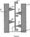
図6に示された特定の実施形態では、記憶容量が、両面(両フェース)型記憶媒体を用いることにより2倍になっている。この場合、データ記録装置は、記憶媒体2の各側に設けられた2つのマイクロティップアレイ(3a,3b)を有している。2つのマイクロティップアレイ3a,3bは好ましくは、フレームの任意の1つのセルと関連したマイクロティップ3a,3bが互いに正確に対向した状態で配置されることはないように側方にずらされている。
In the particular embodiment shown in FIG. 6, the storage capacity is doubled by using a double-sided (both face) type storage medium. In this case, the data recording apparatus has two microtip arrays (3a, 3b) provided on each side of the
図6では、第1のマイクロティップアレイのマイクロティップ3aは、ベース4a中に組み込まれた対応関係をなす電子回路の制御下で読取り又は書き込みを可能にするダイヤフラム2のフェースと接触状態にあり、これに対し、ダイヤフラム2の反対側のフェースと接触状態にある第2のマイクロティップアレイのマイクロティップ3bは、ベース4b中に組み込まれた対応関係にある電子回路の制御下で読取り又は書き込みを可能にする。好ましくは、フレーム1又はベース4a,4bを相互に接合する連結部11により互いにしっかりと固定された2つのマイクロティップアレイをベース4a,4b中に組み込まれた対応関係にある電子回路の制御下で読取り又は書き込み操作中、ダイヤフラムの平面に平行な平面内で移動させることができる。
In FIG. 6, the
代替実施形態では、第1のマイクロティップアレイのマイクロティップ3aは、ダイヤフラム2と接触状態にあり、ベース4a中に組み込まれた対応関係にある電子回路の制御下で読取り又は書き込みを可能にし、これに対し第2のマイクロティップアレイのマイクロティップ3bは、ダイヤフラムから僅かな距離を置いたところに位置する。ダイヤフラム支持フレーム1を第2のマイクロティップアレイ3bの方向でダイヤフラムの平面に垂直に動かすことにより、第1のアレイのマイクロティップ3aはダイヤフラムから遠ざけられ、これに対し、第2のアレイのマイクロティップ3bは、ダイヤフラムと接触してベース4b中に組み込まれた対応関係にある電子回路の制御下で読取り又は書き込みを可能にする。ベース4a,4b相互間の距離は、中央休止位置でダイヤフラムと接触するマイクロティップが存在しないよう選択されたものであるのがよい。フレームの運動に代えて、好ましくはベース4a,4b(連結部11)により互いに固定された2つのマイクロティップアレイを同時に動かしてもよい。
In an alternative embodiment, the
別の代替実施形態では、2つのマイクロティップアレイのベース4a,4bは、互いに固定されない。これらマイクロティップアレイを同時に且つ記憶媒体に対し互いに逆方向に動かすのがよい。第1の位置、即ち休止位置では、2つのベース4a,4bは、フレーム1の平面から分離され、ダイヤフラム2に接触するマイクロティップは存在しない。第2の位置、即ち読取り又は書き込み位置では、2つのベース4a,4bを記憶媒体の方向に動かし、全てのマイクロティップ3a,3bは、ダイヤフラムの両側でダイヤフラムに接触する。この場合、記憶媒体のフェースの各々の読取り及び書き込みは、図6の場合のように、ベース4a,4bにそれぞれ組み込まれた電子回路により制御される。
In another alternative embodiment, the
ベース4内に設けられた電子制御及びアドレス指定回路は、シリコン上に施される任意の技術により達成でき、この場合、マイクロティップ3は、シリコン上に施されるマイクロエレクトロニクス技術により達成される。マイクロティップは例えば、シリコンから作られ、場合によっては、1996年10〜11月発行のD.モロー(D. Moreau )他著,「シリコンマイクロティップの製造プロセス(Procedes de fabrication de micropointes en silicium)」,ル・ビド(Le Vide),282号,P463〜477ページ,ISSN1266−0167又は1998年発行のE.オスターシュルツ(E. Oestershulze)著,「スキャンニング・プローブ・マイクロスコピー用の新規なプローブ(Novel probes for scanning probe microscopy)」,アプライド・フィジクス・エイ・66(Applied Physics A66 ),S3〜S9に記載されているように、導電性及び(又は)硬質材料、例えば窒化チタン(TiN)、炭化タングステン(W2C)又は非晶質ダイヤモンド様炭素(場合によっては導電性であるようドープを行ったダイヤモンド様炭素)で覆われる。
The electronic control and addressing circuit provided in the
マイクロティップが摩耗しないようにするため、マイクロティップを1998年発行のC.ミハルシア(C.Mihalcea)他著,「スキャンニング・プローブ・マイクロスコピー応用用モノリシックプローブの製造(Fabrication of monolithic probes for scanning prove microscopy applications)」,アプライド・フィジクス・A・66(Applied Physics A66 ),S87〜S90に記載された方法に従って中実ダイヤモンドで作ることも計画できる。 In order to prevent the microtip from being worn, the microtip was issued in 1998 by C.I. C. Mihalcea et al., “Fabrication of monolithic probes for scanning prove microscopy applications”, Applied Physics A66, S87. It can also be planned to make solid diamonds according to the method described in ~ S90.
記憶媒体は、可撓性ダイヤフラム2を構成する層のスタックによって形成される。層のスタックは主として、2つの層、即ち、メモリとして働く第1の層及び可撓性ダイヤフラムに或る程度の剛性を与えるよう設計された機械的層と呼ばれる第2の層を含む。メモリの役目を果たす第1の層は、実施される記録技術で決まる材料、例えば、熱可塑性材料、相変化材料、磁性材料等で作られる。他の層は、必要ならば熱的又は電気的機能を実行することができ、或る層は、幾つかの機能に同時に寄与することができる。
The storage medium is formed by a stack of layers that make up the
図7及び図8は、シリコンフレーム1及びフレーム1により支持されたダイヤフラムの機械的層の2つの連続した製作工程を示している。第1の工程では(図7)、機械的層6を厚さ100〜500μmのシリコン層7に〈100〉の配向状態で被着させる。機械的層6は例えば、任意公知の方法、例えば、化学的気相成長法(CVD)又は物理気相成長法(PVD)によりシリコン層7上に被着された非晶質炭素又はダイヤモンド様炭素(DLC)被膜により形成される。次に、セルのパターンを機械的層6と反対側のシリコン層7のフェース上にフォトレジスト法により達成してレジンマスク8を形成する。
7 and 8 show two successive fabrication steps of the
次に、シリコン層7を例えばレジンマスク8を介する水酸化カリウム(KOH)エッチング法により化学的にエッチングする。好ましい結晶面〈111〉に従って行われるエッチングは、選択性があり、ダイヤフラムの機械的層6で止まる。かくして、シリコン層の残りの部分は、内部にセルが生じたフレーム1を形成し、その底部は、このようにしてフレームにより支持されたダイヤフラムの機械的層6によって構成される。
Next, the
図8に示す特定の実施形態では、シリコンの残留層をダイヤフラムの機械的層6と接触した状態に保つ。シリコン9のこの残留層により、ダイヤフラムの剛性を増大させることができ、又は特定の機械的接触を達成することができる。
In the particular embodiment shown in FIG. 8, the residual layer of silicon is kept in contact with the
次に、ダイヤフラムの他の層、即ち、メモリの役目を果たす層及び相補形状の包装層を機械的層6上に達成するのがよい。これら層は場合によっては、シリコン層7のエッチング前に得てもよい。それにもかかわらず、この場合、これら層を例えばシリコン層7上にぴったりと固定されたエンクロージャにより化学的エッチングから保護することが必要である。
Next, the other layers of the diaphragm, that is, the layer serving as a memory and the complementary packaging layer, may be achieved on the
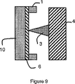
図9に示す変形実施形態では、ダイヤフラムの第1及び第2の層(メモリの機能を実行する層10及び機械的層6)が示され、マイクロティップ3は、機械的層と接触する。これにより、或る場合には相当大きな支承力をマイクロティップと記憶媒体との間に働かせることができるものの、この場合、メモリの役割を果たす層10に応力が加わることはない。かかる支承力は、特に相変化材料上への電気的記録の場合、興味を引くものであることが分かる。機械的層6の厚さにより、マイクロティップ3と接触状態にあるダイヤフラムのフェースと反対側の機械的層のフェースに被着されたメモリの役目を果たす層10に応力を及ぼすことなく、適用可能な力を求めることができる。
In the variant embodiment shown in FIG. 9, the first and second layers of the diaphragm (
かくして、本発明の装置により、用いられる記録技術に応じて弱い支承力と強い支承力の選択を行うことができ、これは、カンチレバーを用いる装置にはできないことである。 Thus, the device of the present invention allows the selection of a weak bearing force and a strong bearing force depending on the recording technology used, which is not possible with a device using a cantilever.
上述の記録装置では、エッジ効果は、マイクロティップ3がフレーム1の近くで可撓性ダイヤフラム2に当接する場合に発生する場合がある。各セル内では、記憶媒体の可撓性は実際に、可撓性ダイヤフラムの中心から縁部まで減少している。走査対象の表面を各セルのダイヤフラムの表面の一部に限定することによりこの効果を制限することができる。しかしながら、かかる制限は、記憶媒体の利用の観点からは最適ではない。
In the recording apparatus described above, the edge effect may occur when the
図10に示す特定の実施形態により、このエッジ効果に関する問題を解決することができる。この装置では、可撓性ダイヤフラムは、第1の場合のようなフレーム1と関連した第1の基本ダイヤフラム2aと、第2の基本ダイヤフラム2bとから成っている。2つの基本ダイヤフラム2a,2bは、フレーム1に対してずらされたスペーサ要素12のアレイによって互いに分離されている。スペーサ要素のアレイを複数の個々のスペーサスタッド12a(図11)によって形成するのがよく、又はかかるスペーサ要素のアレイは、中間フレーム12b(図12)を形成してもよい。スペーサ要素12は、2つの基本ダイヤフラムの変形が生じた場合にこれら2つの基本ダイヤフラム相互間の接触を阻止するのに十分な厚さを有している。
The particular embodiment shown in FIG. 10 can solve this edge effect problem. In this device, the flexible diaphragm consists of a first
かくして、マイクロティップ3は、セルの縁部を境界付けるフレームに向かって移動すると、第2の基本ダイヤフラム2bだけが変形し、支承力は小さいままである。マイクロティップ3がスペーサ要素12の高さ位置で第2の基本ダイヤフラム2bに当接すると、変形は、フレーム1から遠ざかって位置する場所で第1の基本ダイヤフラム2aに伝えられ、その結果、十分な可撓性が得られる。全ての場合において、基本ダイヤフラムのうち少なくとも一方は、マイクロティップの高さのばらつきのために求められる可撓性を保証すると共にかかる高さのばらつきを補償する。かくして、第2の基本ダイヤフラム2bを追加し、これをフレームに対し側方にずらされた場所でのみスペーサ要素12によって第1の基本ダイヤフラム2aに連結することにより形成される二重ダイヤフラムを嵌合フレームと共に用いることによりエッジ効果を無くすことができる。
Thus, when the
この二重ダイヤフラム(2a,12,2b)は、フレーム1及びスペーサ要素12を形成するよう設計されたシリコン層及び基本ダイヤフラム2a,2bを形成するよう設計された上述した形式の薄い材料層を交互に配置することから成る積重ねにより達成できる。かかる積重ねは、任意公知の方法、特にSmart Cut (登録商標)タイプの方法によりシリコンウェーハの連続した切断及び貼り付けによって得ることができる。シリコンは、単一のダイヤフラムの製作に関して図7及び図8を参照して説明した方法と同等の方法により化学的エッチングにより除去できる。このために、スペーサ要素12を形成するよう設計されたシリコン層の等方性エッチングを化学的手段により可能にするようフォトマスキングにより開口部が第1のダイヤフラム2aに設けられる。次に、第1のダイヤフラム2aを部分的に穿孔する。
This double diaphragm (2a, 12, 2b) alternates between a silicon layer designed to form
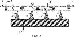
図13及び図14に示す別の特定の実施形態により、マイクロティップ3がフレーム1の近くで可撓性ダイヤフラム2に当接したときに生じるエッジ効果を減少させることができる。スペーサスタッド12aの2次元アレイによりダイヤフラム2から分離された薄い可撓性プレート13のアレイは、各セルを各々が少なくとも1つのマイクロティップと関連した複数の基本セルに細分する。この場合、各セルは、マイクロティップアレイのピッチP1(典型的には、100μm未満)よりも非常に大きな寸法を有するのがよく、その側部の寸法は、例えば最高1cmまでであるのがよい。図13及び図14では、フレーム1によって境界付けられた実質的に正方形のセルは、3つの互いに平行なプレート13の2つの互いに垂直な十文字形の連続体により16個の基本セルに細分されている。実際には、アレイのマイクロティップの数は、約10,000個であり、セルを細分する基本ダイヤフラムの数は、例えば、約100個(10×10)であるのがよい。プレート13の厚さは、大きな寸法の各セルの内部における記憶媒体の高い可撓性を保証するようフレーム1の厚さ(100μm〜500μm)よりも非常に小さい。したがって、上述のエッジ効果は、フレーム1の近くでのみ、即ち、非常に限られた数のマイクロティップ3について生じる場合がある。
Another specific embodiment shown in FIGS. 13 and 14 can reduce the edge effect that occurs when the
プレート13の可撓性は、これらの厚さの3乗の関数であり、これらの幅に比例する。これは又、2つの固定箇所相互間のこれらの長さ、即ち2つのスペーサスタッド12a相互間のこれらの長さで決まる。スペーサスタッドの寸法は、マイクロティップアレイのピッチP1の関数である。プレート13の可撓性を高めるため、幾つかのマイクロティップを各基本セルに関連させることが可能である。組立体の可撓性も又、スペーサスタッドのアレイについて図13及び図14に示すように記憶媒体の平面の2つの寸法方向においてマイクロティップアレイのピッチP1とは僅かに異なるピッチP2を選択することにより高めることができる。この場合、マイクロティップ3がスペーサスタッド12aに向いて配置されている場合、最も近いマイクロティップは、隣のスペーサスタッドに対してずらされる。この場合、マイクロティップ3の高さの相違を吸収するのはダイヤフラム2に固有の可撓性である。
The flexibility of the
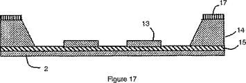
図13及び図14に示すプレートを備えた装置の図15〜図18に示す製作方法によれば、フレーム1及びプレート13は、スペーサスタッド12aの形成のために設計され、それ自体ダイヤフラム2に被着された厚さ100μm〜500μmのシリコンの単一層14中で、厚さ50nm〜500nmの2酸化シリコン層15上に形成される。層15も又、窒化シリコン又は炭素で作られたものであるとよい。
According to the manufacturing method shown in FIGS. 15 to 18 of the apparatus having the plate shown in FIGS. 13 and 14, the
図15及び図16に示す第1の工程では、シリコン層14を、フレーム1及びプレート13の配置場所を保護するマスク16を介して異方性エッチングする。図17に示す第2の工程では、フレーム1だけを保護するマスク17を介してシリコン層14の選択的等方性エッチングによりプレート13を薄くする。図18に示す最後の工程では、マスク(図示せず)を介してスペーサスタッド12aを層15の選択的等方性エッチングにより離脱させ、スペーサスタッドに向いて位置するその領域は、第1の工程の実施中に用いられる図15のマスク16の対応の領域に対して拡大されている。これにより、オーバーエッチング効果を無くすことができ、これは、スペーサスタッド12aにより構成されるアイランド(島状部)の形成を軽減させる。
In the first step shown in FIGS. 15 and 16, the
先の実施形態の場合と同様、例えば、非晶質ダイヤモンド様炭素(DLC)により作られた機械的に剛性な層とメモリ機能を実行する層(プラスチック、相変化材料等)の積重ねによりダイヤフラム2を形成するのがよい。メモリ機能を実行する層を、図18の第3の工程後に被着させるのがよく、この場合、図15の最初の積重ねは、ダイヤフラムの例えば厚さ100nmの剛性機械的層を構成するに過ぎない。
As in the previous embodiment, for example, the
本発明は、上述の特定の実施形態には限定されない。特に、可撓性ダイヤフラム2は、ダイヤモンド様炭素、シリコン、酸化シリコン(SiO2)又は同等な金属から作られた層から成るものであってもよい。ダイヤフラム2の電気的導通が必要な場合、ダイヤフラム2の機械的層6に例えば硼素又は銀をドープするのがよい。
The present invention is not limited to the specific embodiments described above. In particular, the
Claims (19)
Applications Claiming Priority (3)
| Application Number | Priority Date | Filing Date | Title |
|---|---|---|---|
| FR0212275A FR2845512A1 (en) | 2002-10-03 | 2002-10-03 | Equipment for recording data, comprises two dimensional array of microtips which have nanometric apex dimensions and are brought into contact with a flexible diaphragm on frame divided into cells |
| FR0307965A FR2845513B1 (en) | 2002-10-03 | 2003-07-01 | DATA RECORDING DEVICE HAVING MEMBRANE MEMORY MEMORY MEDIUM |
| PCT/FR2003/002879 WO2004032132A2 (en) | 2002-10-03 | 2003-10-01 | Data recording device comprising a diaphragm-type support |
Publications (3)
| Publication Number | Publication Date |
|---|---|
| JP2006502523A JP2006502523A (en) | 2006-01-19 |
| JP2006502523A5 JP2006502523A5 (en) | 2010-04-08 |
| JP4494337B2 true JP4494337B2 (en) | 2010-06-30 |
Family
ID=32031842
Family Applications (1)
| Application Number | Title | Priority Date | Filing Date |
|---|---|---|---|
| JP2005500037A Expired - Fee Related JP4494337B2 (en) | 2002-10-03 | 2003-10-01 | Data recording apparatus having diaphragm type support |
Country Status (6)
| Country | Link |
|---|---|
| US (1) | US7697402B2 (en) |
| EP (1) | EP1547072B1 (en) |
| JP (1) | JP4494337B2 (en) |
| DE (1) | DE60326862D1 (en) |
| FR (1) | FR2845513B1 (en) |
| WO (1) | WO2004032132A2 (en) |
Families Citing this family (6)
| Publication number | Priority date | Publication date | Assignee | Title |
|---|---|---|---|---|
| FR2868411B1 (en) | 2004-04-01 | 2006-06-16 | Commissariat Energie Atomique | FLEXIBLE MEMBRANE COMPRISING DETAILS |
| FR2869027B1 (en) * | 2004-04-15 | 2006-07-14 | Commissariat Energie Atomique | RECORDING SYSTEM HAVING A MEMORY LAYER AND A MICROPOINT NETWORK |
| FR2876831B1 (en) | 2004-10-15 | 2007-02-02 | Commissariat Energie Atomique | DATA RECORDING DEVICE HAVING INCLINED CARBON NANOTUBES AND METHOD FOR MANUFACTURING THE SAME |
| FR2880980B1 (en) | 2005-01-17 | 2007-03-16 | Commissariat Energie Atomique | DATA RECORDING DEVICE COMPRISING MICRO-POINTS WHICH ALL THE FREE TERMINALS FORM A CONVEX SURFACE AND METHOD FOR MANUFACTURING THE SAME |
| FR2880979B1 (en) * | 2005-01-17 | 2007-03-16 | Commissariat Energie Atomique | DATA RECORDING DEVICE HAVING A PERIPHERAL SUPPORT MEMBRANE AND METHOD FOR MANUFACTURING THE SAME |
| FR2910686B1 (en) * | 2006-12-20 | 2009-04-03 | Commissariat Energie Atomique | MEMORIZATION DEVICE WITH MULTI-LEVEL STRUCTURE |
Family Cites Families (16)
| Publication number | Priority date | Publication date | Assignee | Title |
|---|---|---|---|---|
| AT246809B (en) * | 1963-10-18 | 1966-05-10 | Bruno Dipl Ing Woelke | Magnetic recording device |
| FR1519660A (en) * | 1967-01-04 | 1968-04-05 | Vide Soc Gen Du | Improvements to magnetic disk mass memories |
| US3502455A (en) * | 1967-10-09 | 1970-03-24 | Bendix Corp | Method of fabricating a thin film vitreous continuous membrane product |
| US3646533A (en) * | 1969-04-08 | 1972-02-29 | Burroughs Corp | Rotary disk assembly having low-density core for information storage system |
| US4451914A (en) * | 1982-04-15 | 1984-05-29 | Burroughs Corporation | Optical storage system employing a multi-layer optical medium |
| SE463654B (en) * | 1988-03-11 | 1991-01-07 | Nils Goeran Stemme | MEMBRANE STRUCTURE AS WELL AS MANUFACTURING THEM |
| EP0394995B1 (en) * | 1989-04-25 | 1997-07-16 | Canon Kabushiki Kaisha | Information record/reproducing apparatus and information recording carrier |
| US5204581A (en) * | 1990-07-12 | 1993-04-20 | Bell Communications Research, Inc. | Device including a tapered microminiature silicon structure |
| US5216631A (en) * | 1990-11-02 | 1993-06-01 | Sliwa Jr John W | Microvibratory memory device |
| JP3935976B2 (en) * | 1995-02-08 | 2007-06-27 | ヒューレット・パッカード・カンパニー | Semiconductor layer structure and recording medium for large capacity memory device |
| WO1997044780A1 (en) * | 1996-05-20 | 1997-11-27 | International Business Machines Corporation | Shape memory alloy recording medium, storage devices based thereon, and method for using these storage devices |
| US5835477A (en) * | 1996-07-10 | 1998-11-10 | International Business Machines Corporation | Mass-storage applications of local probe arrays |
| US7260051B1 (en) * | 1998-12-18 | 2007-08-21 | Nanochip, Inc. | Molecular memory medium and molecular memory integrated circuit |
| DE10030352A1 (en) * | 2000-06-21 | 2002-01-10 | Bosch Gmbh Robert | Micromechanical component, in particular sensor element, with a stabilized membrane and method for producing such a component |
| US6432740B1 (en) * | 2001-06-28 | 2002-08-13 | Hewlett-Packard Company | Fabrication of molecular electronic circuit by imprinting |
| US20040125733A1 (en) * | 2002-12-31 | 2004-07-01 | Industrial Technology Research Institute | Data storage device utilizing carbon nanotubes and method for operating |
-
2003
- 2003-07-01 FR FR0307965A patent/FR2845513B1/en not_active Expired - Fee Related
- 2003-10-01 DE DE60326862T patent/DE60326862D1/en not_active Expired - Lifetime
- 2003-10-01 WO PCT/FR2003/002879 patent/WO2004032132A2/en active Application Filing
- 2003-10-01 US US10/528,065 patent/US7697402B2/en not_active Expired - Fee Related
- 2003-10-01 EP EP03778382A patent/EP1547072B1/en not_active Expired - Fee Related
- 2003-10-01 JP JP2005500037A patent/JP4494337B2/en not_active Expired - Fee Related
Also Published As
| Publication number | Publication date |
|---|---|
| FR2845513B1 (en) | 2006-08-11 |
| US7697402B2 (en) | 2010-04-13 |
| WO2004032132A3 (en) | 2004-05-27 |
| EP1547072B1 (en) | 2009-03-25 |
| FR2845513A1 (en) | 2004-04-09 |
| US20050269653A1 (en) | 2005-12-08 |
| WO2004032132A2 (en) | 2004-04-15 |
| DE60326862D1 (en) | 2009-05-07 |
| JP2006502523A (en) | 2006-01-19 |
| EP1547072A2 (en) | 2005-06-29 |
Similar Documents
| Publication | Publication Date | Title |
|---|---|---|
| EP1530210B1 (en) | Information recording/reproducing apparatus and recording medium | |
| US6249503B1 (en) | Method of and apparatus for recording/reproducing an information signal, recording/reproducing head device, memory medium, and head element | |
| US5970315A (en) | Microelectromechanical structure and process of making same | |
| JP2004518235A (en) | Molecular storage medium and molecular memory integrated circuit | |
| WO2005020226A1 (en) | Data recording and reproducing device, data recording and reproducing method, and recording medium | |
| US20070121477A1 (en) | Cantilever with control of vertical and lateral position of contact probe tip | |
| Despont et al. | VLSI-NEMS chip for AFM data storage | |
| JP4494337B2 (en) | Data recording apparatus having diaphragm type support | |
| US20030161071A1 (en) | Slider for a data storage device including transducer level micro-positioning and method of fabrication therefor | |
| EP0784847B1 (en) | A memory device | |
| Heck et al. | Ultra-high density MEMS probe memory device | |
| US20130001719A1 (en) | Interaction structure for a storage medium | |
| JP4898436B2 (en) | Data recording method and apparatus with deformable memory support for carrying out this method | |
| KR20060007641A (en) | Nano data writing and reading apparatus using cantilever transfer and manufacturing method thereof | |
| US20090285082A1 (en) | Electric field read/write head, method of manufacturing the electric field read/write head, and information storage device including the electric field read/write head | |
| US20070291623A1 (en) | Cantilever with control of vertical and lateral position of contact probe tip | |
| US7854016B2 (en) | Process for manufacturing probes intended to interact with a storage medium and probe obtained thereby | |
| JP4140598B2 (en) | Recording / playback device | |
| US20070097551A1 (en) | Method and Structure for Integrated High Density Memory Device | |
| US20040196774A1 (en) | Piezoelectric driving type tracking device and method for fabricating the same | |
| US20080037400A1 (en) | Recording System Comprising A Storage Layer And An Array Of Microtips | |
| JP4898705B2 (en) | Data recording apparatus including peripheral supporting thin film and method of manufacturing the apparatus | |
| US7920457B2 (en) | Device for recording data comprising microdots with free ends forming a convex surface and method for the production thereof | |
| Chen et al. | Integrated fabrication of electrostatic microactuator for HDD R/W head positioning | |
| JP3044424B2 (en) | Information processing apparatus and method for manufacturing microtip |
Legal Events
| Date | Code | Title | Description |
|---|---|---|---|
| A621 | Written request for application examination |
Free format text: JAPANESE INTERMEDIATE CODE: A621 Effective date: 20060922 |
|
| A131 | Notification of reasons for refusal |
Free format text: JAPANESE INTERMEDIATE CODE: A131 Effective date: 20091016 |
|
| A601 | Written request for extension of time |
Free format text: JAPANESE INTERMEDIATE CODE: A601 Effective date: 20100114 |
|
| A602 | Written permission of extension of time |
Free format text: JAPANESE INTERMEDIATE CODE: A602 Effective date: 20100121 |
|
| A524 | Written submission of copy of amendment under article 19 pct |
Free format text: JAPANESE INTERMEDIATE CODE: A524 Effective date: 20100216 |
|
| TRDD | Decision of grant or rejection written | ||
| A01 | Written decision to grant a patent or to grant a registration (utility model) |
Free format text: JAPANESE INTERMEDIATE CODE: A01 Effective date: 20100312 |
|
| A01 | Written decision to grant a patent or to grant a registration (utility model) |
Free format text: JAPANESE INTERMEDIATE CODE: A01 |
|
| A61 | First payment of annual fees (during grant procedure) |
Free format text: JAPANESE INTERMEDIATE CODE: A61 Effective date: 20100407 |
|
| R150 | Certificate of patent or registration of utility model |
Free format text: JAPANESE INTERMEDIATE CODE: R150 |
|
| FPAY | Renewal fee payment (event date is renewal date of database) |
Free format text: PAYMENT UNTIL: 20130416 Year of fee payment: 3 |
|
| LAPS | Cancellation because of no payment of annual fees |