JP4892025B2 - Imprint method - Google Patents
Imprint method Download PDFInfo
- Publication number
- JP4892025B2 JP4892025B2 JP2009061650A JP2009061650A JP4892025B2 JP 4892025 B2 JP4892025 B2 JP 4892025B2 JP 2009061650 A JP2009061650 A JP 2009061650A JP 2009061650 A JP2009061650 A JP 2009061650A JP 4892025 B2 JP4892025 B2 JP 4892025B2
- Authority
- JP
- Japan
- Prior art keywords
- photocurable resin
- mold
- region
- pattern
- imprint
- Prior art date
- Legal status (The legal status is an assumption and is not a legal conclusion. Google has not performed a legal analysis and makes no representation as to the accuracy of the status listed.)
- Expired - Fee Related
Links
Images


Classifications
-
- B—PERFORMING OPERATIONS; TRANSPORTING
- B29—WORKING OF PLASTICS; WORKING OF SUBSTANCES IN A PLASTIC STATE IN GENERAL
- B29C—SHAPING OR JOINING OF PLASTICS; SHAPING OF MATERIAL IN A PLASTIC STATE, NOT OTHERWISE PROVIDED FOR; AFTER-TREATMENT OF THE SHAPED PRODUCTS, e.g. REPAIRING
- B29C37/00—Component parts, details, accessories or auxiliary operations, not covered by group B29C33/00 or B29C35/00
- B29C37/0003—Discharging moulded articles from the mould
-
- B—PERFORMING OPERATIONS; TRANSPORTING
- B29—WORKING OF PLASTICS; WORKING OF SUBSTANCES IN A PLASTIC STATE IN GENERAL
- B29C—SHAPING OR JOINING OF PLASTICS; SHAPING OF MATERIAL IN A PLASTIC STATE, NOT OTHERWISE PROVIDED FOR; AFTER-TREATMENT OF THE SHAPED PRODUCTS, e.g. REPAIRING
- B29C37/00—Component parts, details, accessories or auxiliary operations, not covered by group B29C33/00 or B29C35/00
- B29C37/0025—Applying surface layers, e.g. coatings, decorative layers, printed layers, to articles during shaping, e.g. in-mould printing
-
- B—PERFORMING OPERATIONS; TRANSPORTING
- B29—WORKING OF PLASTICS; WORKING OF SUBSTANCES IN A PLASTIC STATE IN GENERAL
- B29C—SHAPING OR JOINING OF PLASTICS; SHAPING OF MATERIAL IN A PLASTIC STATE, NOT OTHERWISE PROVIDED FOR; AFTER-TREATMENT OF THE SHAPED PRODUCTS, e.g. REPAIRING
- B29C37/00—Component parts, details, accessories or auxiliary operations, not covered by group B29C33/00 or B29C35/00
- B29C37/006—Degassing moulding material or draining off gas during moulding
-
- B—PERFORMING OPERATIONS; TRANSPORTING
- B29—WORKING OF PLASTICS; WORKING OF SUBSTANCES IN A PLASTIC STATE IN GENERAL
- B29C—SHAPING OR JOINING OF PLASTICS; SHAPING OF MATERIAL IN A PLASTIC STATE, NOT OTHERWISE PROVIDED FOR; AFTER-TREATMENT OF THE SHAPED PRODUCTS, e.g. REPAIRING
- B29C59/00—Surface shaping of articles, e.g. embossing; Apparatus therefor
- B29C59/02—Surface shaping of articles, e.g. embossing; Apparatus therefor by mechanical means, e.g. pressing
- B29C59/022—Surface shaping of articles, e.g. embossing; Apparatus therefor by mechanical means, e.g. pressing characterised by the disposition or the configuration, e.g. dimensions, of the embossments or the shaping tools therefor
-
- B—PERFORMING OPERATIONS; TRANSPORTING
- B82—NANOTECHNOLOGY
- B82Y—SPECIFIC USES OR APPLICATIONS OF NANOSTRUCTURES; MEASUREMENT OR ANALYSIS OF NANOSTRUCTURES; MANUFACTURE OR TREATMENT OF NANOSTRUCTURES
- B82Y10/00—Nanotechnology for information processing, storage or transmission, e.g. quantum computing or single electron logic
-
- B—PERFORMING OPERATIONS; TRANSPORTING
- B82—NANOTECHNOLOGY
- B82Y—SPECIFIC USES OR APPLICATIONS OF NANOSTRUCTURES; MEASUREMENT OR ANALYSIS OF NANOSTRUCTURES; MANUFACTURE OR TREATMENT OF NANOSTRUCTURES
- B82Y40/00—Manufacture or treatment of nanostructures
-
- G—PHYSICS
- G03—PHOTOGRAPHY; CINEMATOGRAPHY; ANALOGOUS TECHNIQUES USING WAVES OTHER THAN OPTICAL WAVES; ELECTROGRAPHY; HOLOGRAPHY
- G03F—PHOTOMECHANICAL PRODUCTION OF TEXTURED OR PATTERNED SURFACES, e.g. FOR PRINTING, FOR PROCESSING OF SEMICONDUCTOR DEVICES; MATERIALS THEREFOR; ORIGINALS THEREFOR; APPARATUS SPECIALLY ADAPTED THEREFOR
- G03F7/00—Photomechanical, e.g. photolithographic, production of textured or patterned surfaces, e.g. printing surfaces; Materials therefor, e.g. comprising photoresists; Apparatus specially adapted therefor
- G03F7/0002—Lithographic processes using patterning methods other than those involving the exposure to radiation, e.g. by stamping
-
- B—PERFORMING OPERATIONS; TRANSPORTING
- B29—WORKING OF PLASTICS; WORKING OF SUBSTANCES IN A PLASTIC STATE IN GENERAL
- B29C—SHAPING OR JOINING OF PLASTICS; SHAPING OF MATERIAL IN A PLASTIC STATE, NOT OTHERWISE PROVIDED FOR; AFTER-TREATMENT OF THE SHAPED PRODUCTS, e.g. REPAIRING
- B29C35/00—Heating, cooling or curing, e.g. crosslinking or vulcanising; Apparatus therefor
- B29C35/02—Heating or curing, e.g. crosslinking or vulcanizing during moulding, e.g. in a mould
- B29C35/08—Heating or curing, e.g. crosslinking or vulcanizing during moulding, e.g. in a mould by wave energy or particle radiation
- B29C35/0805—Heating or curing, e.g. crosslinking or vulcanizing during moulding, e.g. in a mould by wave energy or particle radiation using electromagnetic radiation
- B29C2035/0822—Heating or curing, e.g. crosslinking or vulcanizing during moulding, e.g. in a mould by wave energy or particle radiation using electromagnetic radiation using IR radiation
-
- B—PERFORMING OPERATIONS; TRANSPORTING
- B29—WORKING OF PLASTICS; WORKING OF SUBSTANCES IN A PLASTIC STATE IN GENERAL
- B29C—SHAPING OR JOINING OF PLASTICS; SHAPING OF MATERIAL IN A PLASTIC STATE, NOT OTHERWISE PROVIDED FOR; AFTER-TREATMENT OF THE SHAPED PRODUCTS, e.g. REPAIRING
- B29C35/00—Heating, cooling or curing, e.g. crosslinking or vulcanising; Apparatus therefor
- B29C35/02—Heating or curing, e.g. crosslinking or vulcanizing during moulding, e.g. in a mould
- B29C35/08—Heating or curing, e.g. crosslinking or vulcanizing during moulding, e.g. in a mould by wave energy or particle radiation
- B29C35/0805—Heating or curing, e.g. crosslinking or vulcanizing during moulding, e.g. in a mould by wave energy or particle radiation using electromagnetic radiation
- B29C2035/0827—Heating or curing, e.g. crosslinking or vulcanizing during moulding, e.g. in a mould by wave energy or particle radiation using electromagnetic radiation using UV radiation
-
- B—PERFORMING OPERATIONS; TRANSPORTING
- B29—WORKING OF PLASTICS; WORKING OF SUBSTANCES IN A PLASTIC STATE IN GENERAL
- B29C—SHAPING OR JOINING OF PLASTICS; SHAPING OF MATERIAL IN A PLASTIC STATE, NOT OTHERWISE PROVIDED FOR; AFTER-TREATMENT OF THE SHAPED PRODUCTS, e.g. REPAIRING
- B29C59/00—Surface shaping of articles, e.g. embossing; Apparatus therefor
- B29C59/02—Surface shaping of articles, e.g. embossing; Apparatus therefor by mechanical means, e.g. pressing
- B29C59/022—Surface shaping of articles, e.g. embossing; Apparatus therefor by mechanical means, e.g. pressing characterised by the disposition or the configuration, e.g. dimensions, of the embossments or the shaping tools therefor
- B29C2059/023—Microembossing
-
- B—PERFORMING OPERATIONS; TRANSPORTING
- B29—WORKING OF PLASTICS; WORKING OF SUBSTANCES IN A PLASTIC STATE IN GENERAL
- B29C—SHAPING OR JOINING OF PLASTICS; SHAPING OF MATERIAL IN A PLASTIC STATE, NOT OTHERWISE PROVIDED FOR; AFTER-TREATMENT OF THE SHAPED PRODUCTS, e.g. REPAIRING
- B29C35/00—Heating, cooling or curing, e.g. crosslinking or vulcanising; Apparatus therefor
- B29C35/02—Heating or curing, e.g. crosslinking or vulcanizing during moulding, e.g. in a mould
- B29C35/08—Heating or curing, e.g. crosslinking or vulcanizing during moulding, e.g. in a mould by wave energy or particle radiation
- B29C35/0888—Heating or curing, e.g. crosslinking or vulcanizing during moulding, e.g. in a mould by wave energy or particle radiation using transparant moulds
Description
本発明は、半導体素子、光素子、バイオ製品等のデバイスの製造に使用されるインプリント方法に関する。 The present invention relates to an imprint method used for manufacturing a device such as a semiconductor element, an optical element, or a bio product.
半導体素子の製造工程において、100nm以下の微細パターンの形成と、量産性とを両立させる技術の一つとして、被転写基板にナノインプリント用モールド(原版、テンプレートとも呼ばれる。)のパターンを転写するナノインプリント技術が注目されている。 Nanoimprint technology for transferring the pattern of a mold for nanoimprint (also referred to as an original plate or a template) to a substrate to be transferred as one of technologies for achieving both the formation of a fine pattern of 100 nm or less and mass productivity in the manufacturing process of a semiconductor element. Is attracting attention.
ナノインプリント技術の一つとして、光(UV)ナノインプリントがある。光ナノインプリントは、被転写基板上に光硬化性樹脂を塗布する工程と、被転写基板とナノインプリント用モールドとを位置合わせする工程(アライメント)と、光硬化性樹脂にナノインプリント用モールドを接触させる工程(インプリント)と、光照射により光硬化性樹脂を硬化する工程と、硬化した光硬化性樹脂(マスク)からナノインプリント用モールドを離す工程(離型)とを含む(特許文献1)。 One of the nanoimprint techniques is optical (UV) nanoimprint. The optical nanoimprint includes a step of applying a photocurable resin on a transfer substrate, a step of aligning the transfer substrate and the nanoimprint mold (alignment), and a step of bringing the nanoimprint mold into contact with the photocurable resin ( (Imprint), a step of curing the photocurable resin by light irradiation, and a step of releasing the nanoimprint mold (release) from the cured photocurable resin (mask) (Patent Document 1).
ここで、幅が狭く高さが高いパターン、つまり、高アスペクト比のパターンが硬化した光硬化性樹脂中に含まれている場合、離型時において、高アスペクト比のパターンがちぎれるなどの欠陥が生じることがある。このような欠陥が生じる理由としては、離型時において、硬化した光硬化性樹脂とナノインプリント用モールドとの間に摩擦力が生じること、硬化した光硬化性樹脂の引っ張り強度はパターン幅が細くなるに連れて弱くなることがあげられる。 Here, when a pattern with a narrow width and a high height, that is, a pattern with a high aspect ratio is contained in the cured photo-curable resin, defects such as tearing of the pattern with a high aspect ratio at the time of release. May occur. The reason why such a defect occurs is that, at the time of mold release, a frictional force is generated between the cured photocurable resin and the nanoimprint mold, and the tensile strength of the cured photocurable resin has a narrow pattern width. Can be weakened with
本発明の目的は、光照射により硬化した光硬化性樹脂(マスクパターン)からインプリント用モールドを離す工程における欠陥の発生を抑制できるインプリント方法を提供することにある。 The objective of this invention is providing the imprint method which can suppress generation | occurrence | production of the defect in the process of releasing the mold for imprint from the photocurable resin (mask pattern) hardened | cured by light irradiation.
本発明の一態様によるインプリント方法は、第1の領域および第2の領域を含む被加工基板上に光硬化性樹脂を塗布すること、前記光硬化性樹脂にインプリント用モールドを接触させること、前記インプリント用モールドを介して前記光硬化性樹脂に光を照射することにより、前記光硬化性樹脂を硬化すること、少なくとも前記第1の領域を含む前記被加工基板の領域上に塗布された前記光硬化性樹脂に所定の処理を加えることによりガスを発生させること、前記第1の領域に塗布された前記光硬化性樹脂から発生する前記ガスの発生量は、前記第2の領域に塗布された前記光硬化性樹脂から発生する前記ガスの発生量よりも多いこと、および前記ガスの発生後、前記光硬化性樹脂から前記インプリント用モールドを離し、前記被加工基板上にパターンを形成することを含み、前記第1の領域は前記第2の領域よりも密度が高いパターンが形成される領域、または、前記第1の領域は前記第2の領域よりもサイズが大きいパターンが形成される領域であることを特徴とする。 In the imprint method according to one aspect of the present invention, a photocurable resin is applied to a substrate to be processed including a first region and a second region, and an imprint mold is brought into contact with the photocurable resin. The photocurable resin is cured by irradiating the photocurable resin with light through the imprint mold, and applied to the region of the substrate to be processed including at least the first region. Generating a gas by applying a predetermined treatment to the photocurable resin; and the amount of the gas generated from the photocurable resin applied to the first region is set in the second region. More than the amount of the gas generated from the applied photocurable resin, and after the generation of the gas, the imprint mold is separated from the photocurable resin, and on the substrate to be processed Look including forming a pattern, the first region is a region wherein the second density is higher than the region pattern is formed, or the first region is larger in size than said second region It is a region where a pattern is formed .
本発明によれば、光照射により硬化した光硬化性樹脂(マスクパターン)からインプリント用モールドを離す工程における欠陥の発生を抑制できるインプリント方法を実現できるようになる。 ADVANTAGE OF THE INVENTION According to this invention, the imprint method which can suppress generation | occurrence | production of the defect in the process of separating the mold for imprint from the photocurable resin (mask pattern) hardened | cured by light irradiation can be implement | achieved.
以下、図面を参照しながら本発明の実施形態を説明する。 Hereinafter, embodiments of the present invention will be described with reference to the drawings.
(第1の実施形態)
図1−図8は、第1の実施形態に係るインプリント方法を用いたパターン形成方法を示す断面図である。
(First embodiment)
1 to 8 are sectional views illustrating a pattern forming method using the imprint method according to the first embodiment.
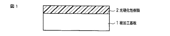
[図1]
被加工基板1上に光硬化性樹脂2が塗布される。
[Figure 1]
A
被加工基板1は、例えば、石英基板(透明基板)、シリコン基板(半導体基板)、SOI基板(半導体基板)である。被加工基板1は、多層構造のものであっても構わない。例えば、上記透明基板もしくは上記半導体基板と、その上に設けられた絶縁膜またはマスクとで構成されたもの(多層構造の被加工基板)であっても構わない。
The
上記絶縁膜は、例えば、ハードマスクとなるシリコン窒化膜とシリコン酸化膜との積層膜、または、層間絶縁膜としてのシリコン酸化膜もしくはlow−k(低誘電率)膜である。上記マスクは、例えば、有機膜で構成されたマスクである。さらに、被加工基板1の最上層の下には、デバイス製造過程で形成されたデバイスパターンが存在していても構わない。
The insulating film is, for example, a laminated film of a silicon nitride film and a silicon oxide film serving as a hard mask, or a silicon oxide film or a low-k (low dielectric constant) film as an interlayer insulating film. The mask is, for example, a mask made of an organic film. Furthermore, a device pattern formed in the device manufacturing process may exist under the uppermost layer of the
光硬化性樹脂2は、光照射により硬化すると、内部からガスが発生する。このようなガス(アウトガス)を発生する光硬化性樹脂2としては、例えば、ESCAP構造を有する有機材料があげられる。
When the
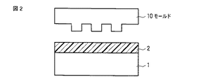
[図2]
被加工基板1と光インプリント用モールド(以下、モールドという。)10との位置合わせ(アライメント)が行われる。モールド10は、表面にパターン(凹凸)が形成された透明基板で構成されている。上記パターンは、高アスペクト比(例えば、3以上)のパターンを含む。上記透明基板は、例えば、石英基板である。透明基板の材料は、照射する光に対応して適宜変更可能である。透明基板の表面に形成されたパターン(凹凸)は、被加工基板1上に形成するべきパターン(凹凸)に対応する。
[Figure 2]
Position alignment (alignment) between the
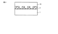
[図3]
光硬化性樹脂2にモールド10を接触させる(インプリント)。このとき、モールド10の凸部と被加工基板1との間(隙間)には光硬化性樹脂2が薄く残る。この薄く残った光硬化性樹脂2は残膜となる。
[Fig. 3]
The
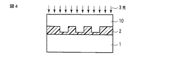
[図4]
光硬化性樹脂2に光(UV〜EUVを含む)3を照射することにより、光硬化性樹脂2の硬化が行われる。UV光の波長は例えば310nmである。
[Fig. 4]
The
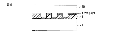
[図5]
光硬化性樹脂2は、光照射により硬化すると、アウトガスを発生するので、光照射後には、光硬化性樹脂2とモールド10との間にアウトガス4が溜まる。この溜まったアウトガス4(アウトガス層)は、図5では、簡単のため、特にアウトガスが発生しやすい領域のものしか示していない。アウトガス4はその体積を広げようとするので、光硬化性樹脂2とモールド10との間の密着力は弱められる。また、アウトガス4が抜けたところに外気のガスが入ることでも、光硬化性樹脂2とモールド10との間の密着力は弱まる。
[Fig. 5]
Since the
[図6]
光硬化性樹脂2からモールド10が離される(離型)。
[Fig. 6]
The
このとき、アウトガス4によって、光硬化性樹脂2とモールド10との間の密着力は弱まっている。そのため、従来よりも弱い力(引っ張り力)で、光硬化性樹脂2からモールド10を離すことができる。したがって、本実施形態によれば、離型時において、高アスペクト比のパターンがちぎれるなどの欠陥(パターン剥がれ)の発生を抑制できるようになる。
At this time, the adhesion between the
図9−図11に、離型時において発生しうる欠陥(パターン剥がれ)の例を示す。 FIG. 9 to FIG. 11 show examples of defects (pattern peeling) that can occur during mold release.
図9は、光硬化性樹脂2に形成された高アスペクト比のパターンがちぎれる欠陥を示している。
FIG. 9 shows defects in which a high aspect ratio pattern formed on the
図10は、光硬化性樹脂2に形成された高アスペクト比のパターンおよびその周囲の部分が除去される欠陥を示している。
FIG. 10 shows a defect in which a pattern with a high aspect ratio formed on the
図11は、被加工基板1が多層構造(図11は2層1a,1bの例)の場合において、光硬化性樹脂2に形成された高アスペクト比のパターンおよびその周囲の部分、さらにその下地の部分1bが除去される欠陥を示している。下地の部分1bが除去されるのは、被加工基板1の多層構造の各層間の密着性が弱いと、密着力が最も弱い層間(図11は層1a,1b間の例)の界面で剥がれが生じるからである。
FIG. 11 shows a high aspect ratio pattern formed on the
[図7]
残った光硬化性樹脂2(残膜)が除去され、硬化した光硬化性樹脂からなるマスク(光硬化性樹脂マスク)2が得られる。上記の残膜の除去は、例えば、主に酸素プラズマによる異方性エッチングを用いて行われる。
[Fig. 7]
The remaining photocurable resin 2 (residual film) is removed, and a mask (photocurable resin mask) 2 made of the cured photocurable resin is obtained. The removal of the residual film is performed, for example, mainly using anisotropic etching with oxygen plasma.
[図8]
光硬化性樹脂マスク2をエッチングマスクに用いて、被加工基板1をエッチングすることにより、被加工基板1上に微細パターンが形成される。その後、光硬化性樹脂マスク2が除去される。本実施形態によれば、離型時における欠陥(パターン剥がれ)の発生を抑制できるので、欠陥が無い高品質の微細パターンを形成できる。これにより、製品の歩留まりを向上できる。
[Fig. 8]
A fine pattern is formed on the
ここで、被加工基板1が透明基板または半導体基板の場合、透明基板または半導体基板がエッチングされる。一方、被加工基板1が多層構造の場合、例えば、透明基板/絶縁膜または半導体基板/絶縁膜の場合、絶縁膜がエッチングされる。これにより、光硬化性樹脂マスク2のパターンが転写された絶縁膜(ハードマスク)が得られる。その後、このハードマスクを用いて、透明基板または半導体基板をエッチングすることにより、微細パターンが形成される。
Here, when the
本実施形態では、モールド10の凸部の断面形状が矩形状であるが、その形状は形成するべきデバイスのパターン(デバイスパターン)によって適宜変更される。例えば、CCDに用いられるマイクロレンズアレイの場合であれば、モールド10の凸部の側面は円弧状の形状を含む。
In the present embodiment, the cross-sectional shape of the convex portion of the
本実施形態のパターン方法は、マイクロレンズアレイ(光素子)以外にも、半導体デバイス(例えばCMOSロジックを構成するMOSトランジスタ)、DNAチップ(バイオ製品)を構成するSiウェハ上に形成されるパターンにも適用できる(他の実施形態も同様)。 In addition to the microlens array (optical element), the pattern method of the present embodiment uses a pattern formed on a Si wafer constituting a semiconductor device (for example, a MOS transistor constituting a CMOS logic) and a DNA chip (bio product). Can also be applied (the same applies to other embodiments).
また、図5の工程の後で、光硬化性樹脂2とモールド10との間の密着力を評価しても構わない(他の実施形態も同様)。すなわち、図5の工程の後で、光硬化性樹脂2とモールド10との間の密着力が一定値(しきい値)以下になった否かの判断(判断工程)を行っても構わない。上記一定値(しきい値)は、離型時において欠陥(パターン剥がれ)が発生しない値に設定される。
Moreover, you may evaluate the adhesive force between the
具体的には、モールド10側から光硬化性樹脂2上に光を照射し、その反射光の強度に基づいてアウトガス4の量を見積もる。見積もったアウトガス4の量が所定値以上の場合であれば、密着力は一定値以下になったと判断し、図6の工程(離型)に進む。見積もったアウトガス4の量が所定値未満の場合には、光硬化性樹脂2に光3をさらに照射(再照射)して、アウトガス4をさらに発生させる。
Specifically, light is irradiated onto the
他の判断方法としては、図6の工程(離型)で、モールド10を所定の力で引っ張って、光硬化性樹脂2からモールド10を離す際に、モールド10を上記所定の力よりも弱い予め決められた力で引っ張って、光硬化性樹脂2からモールド10が全く離れなかった場合には、密着力は弱まっていないと判断し、この場合には、光硬化性樹脂2に光3をさらに照射して、アウトガス4をさらに発生させる。
As another determination method, when the
(第2の実施形態)
図12−図15は、第2の実施形態に係るインプリント方法を用いたパターン形成方法を示す断面図である。なお、以下の図において、既出の図と対応する部分には既出の図と同一符号を付してあり、詳細な説明は省略する。
(Second Embodiment)
12 to 15 are cross-sectional views illustrating a pattern forming method using the imprint method according to the second embodiment. In the following drawings, the same reference numerals as those in the previous drawings are attached to portions corresponding to those in the previous drawings, and detailed description thereof is omitted.
[図12]
被加工基板1上に光硬化性樹脂2が塗布される。
[Fig. 12]
A
光硬化性樹脂2を光触媒層と接触した状態で光照射により硬化すると、光触媒層がない場合と比べて、光硬化性樹脂2はより多くのアウトガスを発生する。このようにしてアウトガスを効果的に発生させるためには、光硬化性樹脂2は例えばESCAP構造を有する有機材料で形成し、また、光触媒層としては例えば酸化チタン層を用いる。
When the
被加工基板1とモールド10との位置合わせ(アライメント)が行われる。
Position alignment (alignment) between the
モールド10のパターン面(凹凸パターン)は光触媒層11で覆われている。光触媒層11は、上記の通り、例えば、酸化チタン層である。酸化チタン層の形成工程は、モールド10のパターン面上にチタン層を堆積する工程と、上記チタン層を酸化する工程とを含む。
The pattern surface (uneven pattern) of the
酸化チタン層は、チタン層の堆積工程とチタン層の酸化工程とに分けなくても、形成することができる。例えば、スパッタ法を用いる場合であれば、Tiからなるターゲットを用い、微量の酸素ガスを真空チャンバー内に導入することで、TiO2 層を形成することができる。また、EB蒸着法を用いる場合であれば、焼成によって形成したTiO2 の結晶粉末をタブレット状に固めたものをターゲットとして用いれば、TiO2 層を形成することができる。 The titanium oxide layer can be formed without being divided into a titanium layer deposition step and a titanium layer oxidation step. For example, if a sputtering method is used, a TiO2 layer can be formed by using a target made of Ti and introducing a small amount of oxygen gas into the vacuum chamber. In the case of using the EB vapor deposition method, a TiO2 layer can be formed by using as a target a TiO2 crystal powder formed by firing, which is solidified in a tablet shape.
[図13]
光硬化性樹脂2にモールド10を接触させる(インプリント)。
[Fig. 13]
The
光硬化性樹脂2に光3を照射することにより、光硬化性樹脂2の硬化が行われる。
By irradiating the
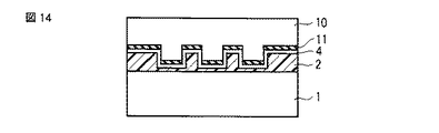
[図14]
光硬化性樹脂2を光触媒層11と接触した状態で光照射により硬化すると、光硬化性樹脂2はアウトガスを発生するので、光照射後には、光硬化性樹脂2と光触媒層11との間にアウトガス4が溜まる。アウトガス4はその体積を広げようとするので、光硬化性樹脂2と光触媒層11との間、つまり、光硬化性樹脂2とモールド10との間の密着力は弱められる。
[FIG. 14]
When the
[図15]
光硬化性樹脂2からモールド10が離される(離型)。
[FIG. 15]
The
このとき、アウトガスによって、光硬化性樹脂2とモールド10との間の密着力は弱まっている。そのため、従来よりも弱い力(引っ張り力)で、光硬化性樹脂2からモールド10を離すことができる。したがって、本実施形態によれば、離型時において、高アスペクト比のパターンがちぎれるなどの欠陥(パターン剥がれ)の発生を抑制できるようになる。
At this time, the adhesion force between the
この後は、第1の実施形態と同様に、図7の工程(残膜の除去)、図8の工程(被加工基板のエッチング)などが行われる。 Thereafter, as in the first embodiment, the process of FIG. 7 (removal of remaining film), the process of FIG. 8 (etching of the substrate to be processed), and the like are performed.
本実施形態でも第1の実施形態と同様に、離型時における欠陥(パターン剥がれ)の発生を抑制できるので、欠陥が無い高品質の微細パターンを形成でき、その結果として、製品の歩留まりを向上できるようになる。 In this embodiment as well as the first embodiment, the occurrence of defects (pattern peeling) at the time of mold release can be suppressed, so that a high-quality fine pattern having no defects can be formed, and as a result, the yield of products is improved. become able to.
なお、本実施形態では、光触媒層11が形成されたモールド10を用いたが、モールド10に光触媒層11を形成する代わりに、光硬化性樹脂2の表面上に光触媒層11する方法でも、本実施形態と同様の効果が得られる。さらに、モールド10および光硬化性樹脂2の両方に光触媒層11を形成しても構わない。
In this embodiment, the
(第3の実施形態)
図16−図23、第3の実施形態に係るインプリント方法を用いたパターン形成方法を示す断面図である。
(Third embodiment)
16 to 23 are cross-sectional views illustrating a pattern forming method using the imprint method according to the third embodiment.
[図16]
被加工基板1上に光硬化性樹脂2aが塗布される。
[FIG. 16]
A
光硬化性樹脂2aはナフトキノンジアジド化合物を含む。より具体的には、光硬化性樹脂2aは、ベンゾフェノンにナフトキノンジアジドを結合させた化合物(ナフトキノンジアジド化合物)を溶剤に溶かしたものである。ナフトキノンジアジド化合物が光硬化性樹脂2aの表層に偏在するように、ナフトキノンジアジド化合物を含むインプリント材料を被加工基板1上の塗布(滴下)することが好ましい。
The
図24に示すように、ナフトキノンジアジド化合物は光(hν)が照射されると、インデンカルボン酸に変化する。ナフトキノンジアジド化合物は、インデンカルボン酸に変化するときに、窒素ガスを放出する。したがって、光硬化性樹脂2aは、光照射により硬化すると、アウトガス(窒素ガス)を発生する。
As shown in FIG. 24, the naphthoquinonediazide compound changes to indenecarboxylic acid when irradiated with light (hν). Naphthoquinone diazide compounds release nitrogen gas when converted to indenecarboxylic acid. Therefore, the
[図17]
被加工基板1とモールド10との位置合わせが行われる。
[Fig. 17]
Position alignment with the to-
[図18]
光硬化性樹脂2aにモールド10を接触させる(インプリント)。
[FIG. 18]
The
[図19]
光硬化性樹脂2aに光3を照射することにより、光硬化性樹脂2aの硬化が行われる。
[FIG. 19]
By irradiating the
[図20]
光硬化性樹脂2aは、光照射により硬化すると、アウトガス(窒素ガス)を発生するので、光照射後には、光硬化性樹脂2aとモールド10との間にアウトガス(窒素ガス)4aが溜まる。アウトガス4aはその体積を広げようとするので、光硬化性樹脂2aとモールド10との間の密着力は弱められる。アウトガス4aを効果的に発生させるためには、光3の波長は300−450nmが好ましい。
[FIG. 20]
When the
[図21]
光硬化性樹脂2aからモールド10が離される(離型)。
[FIG. 21]
The
このとき、アウトガス4aによって、光硬化性樹脂2aとモールド10との間の密着力は弱まっている。そのため、従来よりも弱い力(引っ張り力)で、光硬化性樹脂2aからモールド10を離すことができる。したがって、本実施形態によれば、離型時において、高アスペクト比のパターンがちぎれるなどの欠陥(パターン剥がれ)の発生を抑制できるようになる。
At this time, the adhesion force between the
ここで、光硬化性樹脂2a中にナフトキノンジアジド化合物を5mol%添加した場合には、離型を行う際のアウトガス(窒素ガス)によるアシスト力は約150Nとなり、欠陥(パターン剥がれ)の発生を効果的に抑制できる。なお、ナフトキノンジアジド化合物の添加量が0.1mol%以上であれば、欠陥発生抑制の効果は得られる。
Here, when 5 mol% of a naphthoquinone diazide compound is added to the photo-
[図22]
残った光硬化性樹脂2a(残膜)が除去され、光硬化性樹脂からなるマスク(光硬化性樹脂マスク)2aが得られる。
[FIG. 22]
The remaining
[図23]
光硬化性樹脂マスク2aをエッチングマスクに用いて、被加工基板1をエッチングすることにより、被加工基板1上にパターンが形成される。その後、光硬化性樹脂マスク2aが除去される。
[FIG. 23]
A pattern is formed on the processed
本実施形態によれば、離型時における欠陥(パターン剥がれ)の発生を抑制できるので、欠陥が無い高品質の微細パターンを形成できる。これにより、製品の歩留まりを向上できる。 According to this embodiment, since the occurrence of defects (pattern peeling) at the time of mold release can be suppressed, a high-quality fine pattern having no defects can be formed. Thereby, the yield of a product can be improved.
なお、本実施形態では、全ての領域に対して光硬化性樹脂2aを使用したが、所定の領域に対してだけ光硬化性樹脂2aを使用し、残りの領域に対してはアウトガスを発生しない通常の光硬化性樹脂を使用しても構わない。
In the present embodiment, the
上記所定の領域は、例えば、離型力が大きい領域であり、具体的には、密度の高いパターンを含む領域(密パターン領域)である。密度の高いパターンは表面積が大きいので、大きな離型力が必要となる。なお、離型力は、光照射により硬化された光硬化性樹脂からモールドを離す工程において、前記光硬化性樹脂からモールドを離すために要する力である。 The predetermined region is, for example, a region having a large release force, and specifically, a region including a pattern having a high density (dense pattern region). Since a high density pattern has a large surface area, a large release force is required. The mold release force is a force required to release the mold from the photocurable resin in the step of releasing the mold from the photocurable resin cured by light irradiation.
このように離型力が大きい領域に対してだけ光硬化性樹脂2aを使用することにより、モールド10のパターン面内での離型力のばらつきが小さくなり、離型時におけるモールド10の歪みを小さくできるので、離型欠陥の発生を抑制できるようになる。同様の効果は、モールドのパターン面の全面をDNQが含有した溶液で処理後、密パターンの部分を選択的に露光することでN2 を発生させたテンプレートを使用した場合でも確認することができた。
Thus, by using the
(第4の実施形態)
図25−図30は、第4の実施形態に係るインプリント方法を用いたパターン形成方法を示す断面図である。
(Fourth embodiment)
25 to 30 are cross-sectional views illustrating a pattern forming method using the imprint method according to the fourth embodiment.
[図25]
被加工基板1上に、ナフトキノンジアジド化合物を含まない光硬化性樹脂2bが塗布される。
[FIG. 25]
A
光硬化性樹脂2上にナフトキノンジアジド化合物を含む光硬化性樹脂2cが塗布される。スキャンノズル20を用いて、光硬化性樹脂2b上にナフトキノンジアジド化合物を含むインプリント材を滴下することで、光硬化性樹脂2cは塗布される。
A photocurable resin 2 c containing a naphthoquinonediazide compound is applied on the
[図26]
被加工基板1とモールド10との位置合わせが行われる。
[FIG. 26]
Position alignment with the to-
[図27]
光硬化性樹脂2b,2cにモールド10を接触させる(インプリント)。
[FIG. 27]
The
[図28]
光硬化性樹脂2b,2bに光3を照射することにより、光硬化性樹脂2b,2cの硬化が行われる。
[FIG. 28]
By irradiating the
光硬化性樹脂2cは、光照射により硬化すると、アウトガス(窒素ガス)を発生するので、光照射後には、光硬化性樹脂2b,2cとモールド10との間にアウトガス(窒素ガス)4aが溜まる。アウトガス4aはその体積を広げようとするので、光硬化性樹脂2b,2cとモールド10との間の密着力は弱められる。
Since the photocurable resin 2c generates outgas (nitrogen gas) when cured by light irradiation, after the light irradiation, the outgas (nitrogen gas) 4a accumulates between the
[図29]
光硬化性樹脂2b,2cからモールド10が離される(離型)。
[FIG. 29]
The
このとき、アウトガス4aによって、光硬化性樹脂2b,2cとモールド10との間の密着力は弱まっている。そのため、従来よりも弱い力(引っ張り力)で、光硬化性樹脂2b,2cからモールド10を離すことができる。したがって、本実施形態によれば、離型時において、高アスペクト比のパターンがちぎれるなどの欠陥(パターン剥がれ)の発生を抑制できるようになる。
At this time, the adhesion between the
ここで、光硬化性樹脂2c中にナフトキノンジアジド化合物を5mol%添加した場合には、離型を行う際のアウトガス(窒素ガス)によるアシスト力は約150Nとなり、欠陥(パターン剥がれ)の発生を効果的に抑制できる。 Here, when 5 mol% of a naphthoquinone diazide compound is added to the photocurable resin 2c, the assisting force due to outgas (nitrogen gas) at the time of mold release is about 150 N, which is effective in generating defects (pattern peeling). Can be suppressed.
[図30]
残った光硬化性樹脂2b,2c(残膜)が除去され、光硬化性樹脂からなるマスク(光硬化性樹脂マスク)2b,2cが得られる。
[FIG. 30]
The remaining
光硬化性樹脂マスク2b,2cをエッチングマスクに用いて、被加工基板1をエッチングすることにより、被加工基板1上にパターンが形成される。その後、光硬化性樹脂マスク2が除去される。
A pattern is formed on the processed
本実施形態でも第3の実施形態と同様に、離型時における欠陥(パターン剥がれ)の発生を抑制できるので、欠陥が無い高品質の微細パターンを形成できる。これにより、製品の歩留まりを向上できる。 Similarly to the third embodiment, since the occurrence of defects (pattern peeling) at the time of mold release can be suppressed in this embodiment as well, a high-quality fine pattern having no defects can be formed. Thereby, the yield of a product can be improved.
(第5の実施形態)
図31は、第5の実施形態に係るインプリント方法を用いたパターン形成方法を示す断面図である。
(Fifth embodiment)
FIG. 31 is a cross-sectional view showing a pattern forming method using the imprint method according to the fifth embodiment.
本実施形態が第1−第4の実施形態と異なる点は、熱を発生する熱発生部材12を含むモールド10を用いることにある。熱発生部材12により発生した熱により、離型時において、光硬化性樹脂2は直接または間接的に加熱される。光硬化性樹脂2が間接的に加熱されるとは、熱発生部材12により発生した熱により、モールド10または被加工基板1が加熱され、モールド10または被加工基板1の温度が上がり、その結果として、光硬化性樹脂2は加熱されることである。
The present embodiment is different from the first to fourth embodiments in that a
熱発生部材12は、例えば、赤外光を吸収する赤外吸収体である。赤外吸収体の材料としては、例えば、炭素(黒鉛)があげられる。赤外光を吸収した赤外吸収体は、熱(輻射熱)を発生する。なお、光硬化性樹脂2を硬化するための光は、上記赤外吸収体を通過する。上記赤外光は、離型時に、図示しない赤外光源により上記赤外吸収体に照射される。熱発生部材12は、抵抗ヒーターであっても構わない。
The
本実施形態によれば、熱発生部材12により発生した熱により、光硬化性樹脂2中に残存していた溶媒、例えば、PGMEA(プロピレングリコールモノメチルエーテルアセテート)が気化される。その結果、モールド10と光硬化性樹脂2との界面にアウトガスが溜まる。このアウトガスによって、離型時における光硬化性樹脂2とモールド10との間の密着力が弱まるので、第1の実施形態等と同様に、離型時における欠陥(離型欠陥)の発生を抑制できる。アウトガスは、モールド10に接した光硬化性樹脂2の表面から発生するので、光硬化性樹脂2の内部でガス発生し、該内部にガスが残るという欠陥(空隙)の発生は抑制される。
According to this embodiment, the solvent generated in the
熱発生部材12として、赤外吸収体を用いた場合には、赤外吸収体の面積(光硬化性樹脂2との対向面積)を大きくすることにより、光硬化性樹脂2をまんべんなく加熱することが可能となる。これにより、アウトガスを均一に発生させることができ、欠陥をさらに減らすことができるようになる。
When an infrared absorber is used as the
(第6の実施形態)
図32は、第6の実施形態に係るインプリント方法を用いたパターン形成方法を示す断面図である。
(Sixth embodiment)
FIG. 32 is a cross-sectional view showing a pattern forming method using the imprint method according to the sixth embodiment.
本実施形態が第5の実施形態と異なる点は、冷媒によって温度を下げられる機構を備えたチャック30を用いることにある。ここでは、上記機構として、冷媒を流すための配管31を用いた例について説明する。上記冷媒は、例えば、代替フロン冷媒であり、図示しない冷媒供給装置により、配管31中に供給されるようになっている。
This embodiment is different from the fifth embodiment in that a
被加工基板1をチャック30上に固定した状態で、光硬化性樹脂2の塗布工程から光照射による光硬化性樹脂2の硬化工程までを行う。続いて、配管31中に冷媒を流し、チック31を冷却することにより、被加工基板11、光硬化性樹脂2およびモールド10の熱膨張を抑制する。その後、離型を行う。これにより、熱発生部材12による加熱で生じうるアライメント精度を低下させずに、離型欠陥を抑制できるようになる。
In a state where the
なお、次のショット(インプリント)を行う前に、図33に示すように、容器40内に入った冷却剤としての液体41中にモールド10を浸し、その後、液体41からモールド10を取り出し、図34に示すように、エアー42によりモールド10を乾燥させても構わない。これにより、モールド10の膨張によるアライメント精度の低下をより効果的に抑制できるようになる。
Before performing the next shot (imprint), as shown in FIG. 33, the
(第7の実施形態)
図35は、第7の実施形態に係るインプリント方法を用いたパターン形成方法を示す断面図である。
(Seventh embodiment)
FIG. 35 is a cross-sectional view showing a pattern forming method using the imprint method according to the seventh embodiment.
本実施形態が第1の実施形態と異なる点は、モールド10の凸部および凹部の上に半透明膜5が設けられていることにある。半透明膜5は、例えば、波長365nmの光(光硬化性樹脂2を硬化するための光(UV光)3)に対して5%の透過率を有する。
The present embodiment is different from the first embodiment in that the translucent film 5 is provided on the convex and concave portions of the
図36は、図35の破線で囲まれた領域の拡大図である。 FIG. 36 is an enlarged view of a region surrounded by a broken line in FIG.
光3は、半透明膜5の上面を照射する光(垂直成分の光)3aと、半透明膜5を照射しない光(斜め成分の光)3bとを含む。光3aは半透明膜5を透過してその強度が弱まるので、半透明膜5下の光硬化性樹脂2は十分には硬化されない。ここでは、半透明膜5下の光硬化性樹脂2が硬化されないように、光3の照射量を設定する。一方、光3bは半透明膜5を通らないので、光3bが照射される部分の光硬化性樹脂2は十分に硬化される。
The
したがって、半透明膜5を介して対向した部分のモールド10と光硬化性樹脂2との間の密着力は弱くなるので、離型時における離型欠陥の発生を抑制できるようになる。
Therefore, since the adhesive force between the
ここで、例えば、第5の実施形態で述べたように、光硬化性樹脂2を赤外線で加熱すれば、半透明膜5下の未硬化の光硬化性樹脂2からガスが発生するので、離型時における離型欠陥の発生をより効果的に抑制できるようになる。
Here, for example, as described in the fifth embodiment, if the
なお、本実施形態では、モールド10の凸部および凹部の上に半透明膜5を設けたが、凸部および凹部の一方でも構わない。また、半透明膜5の代わりに、光硬化性樹脂2を硬化するための光を遮光する遮光膜を用いても構わない。
In the present embodiment, the translucent film 5 is provided on the convex portion and the concave portion of the
(第8の実施形態)
図37は、第8の実施形態に係るインプリント方法を用いたパターン形成方法を示す断面図である。
(Eighth embodiment)
FIG. 37 is a cross-sectional view showing a pattern forming method using the imprint method according to the eighth embodiment.
本実施形態が第1−第7の実施形態と異なる点は、ガスを発生させることができる被膜13で、モールド10のパターン面をコーティングすることにある。被膜13の材料としては、例えば、通常状態(光が照射されていない状態)ではガスを吸着し、光が照射されるとガスを発生するものがあげられる。ここでは、光3を照射してもガスを発生しない光硬化性樹脂2dを用いる。
This embodiment is different from the first to seventh embodiments in that the pattern surface of the
このような材料で形成された被膜13でパターン面を被覆すると、光硬化性樹脂2にモールド10を接触させる工程(インプリント)までの間に、モールド10がおかれている雰囲気中に存在するガスが被膜13の表面に吸着される。
When the pattern surface is covered with the
インプリント後に行われる、光照射による光硬化性樹脂2dの際には、被膜13に光が照射されるので、被膜13の表面から上記ガスは脱着する。この脱着したガスはアウトガスとして働くため、離型時における光硬化性樹脂2dとモールド10との間の密着力は弱くなる。したがって、離型欠陥の発生を抑制できる。
In the case of the
本実施形態では、光硬化性樹脂2dを硬化するための光3の照射により、被膜13の表面からガスが脱着する場合について説明したが、光硬化性樹脂2dを硬化するための光3の照射ではガスの脱着は起こらず、光3とは波長が異なる光(ガス脱着用光)の照射でガスの脱着が生じる被膜を用いても構わない。
In the present embodiment, the case where gas is desorbed from the surface of the
このような被膜を用いた場合、光3の照射による光硬化性樹脂2dの後に、ガス脱着用光の照射によるガス脱着を行うことができる。この時、光3の照射時間よりもガス脱着用光の照射時間を長くすることにより、より多くのガスを発生させることができる。したがって、離型時欠陥の発生をより効果的に抑制できる。
When such a film is used, gas desorption by irradiation with gas desorption light can be performed after the
なお、本実施形態では、モールド10のパターン面の全体を被膜13でコーティングしたが、パターン面の一部を被膜13でコーティングしても構わない。また、光照射によりガスを発生する光硬化性樹脂2を用いても構わない。
In the present embodiment, the entire pattern surface of the
(第9の実施形態)
図38は、第9の実施形態に係るインプリント方法を用いたパターン形成方法を示す断面図である。
(Ninth embodiment)
FIG. 38 is a cross-sectional view showing a pattern forming method using the imprint method according to the ninth embodiment.
本実施形態が第1−第8の実施形態と異なる点は、モールド10の凹部に位相/透過率調整膜14が設けられていることにある。位相/透過率調整膜14は、光3の位相および透過率の少なくとも一方を調整する。位相/透過率調整膜14の材料は、例えば、MoSi、SiN、CrまたはCrOである。
The present embodiment is different from the first to eighth embodiments in that the phase /
位相/透過率調整膜14の光学パラメータ(例えば、屈折率n、減衰係数k)、モールド10の凹部と被加工基板1との距離L1、モールド10の凸部と被加工基板1との距離L2、光3の波長(硬化波長)、モールド10の屈折率、光硬化性樹脂2の屈折率などを考慮して、位相/透過率調整膜14を設計することにより、モールド10の凹部と光硬化性樹脂2との界面近傍に、光3の定在波のピークを生じさることができる。例えば、硬化波長が310nm、モールド10の屈折率が1.5(石英屈折率)、光硬化性樹脂2の屈折率が1.45であれば、上記界面近傍に光3の定在波のピークを生じさることができる。
Optical parameters (for example, refractive index n, attenuation coefficient k) of the phase /
モールド10の凹部と光硬化性樹脂2との界面近傍に、光3の定在波のピークを生じることで、モールド10の凹部と光硬化性樹脂2との界面近傍でのアウトガスの発生量を多くできる。したがって、離型欠陥の発生を効果的に抑制できるようになる。
By generating a standing wave peak of
なお、本実施形態では、モールド10の凹部に位相/透過率調整膜14を設けたが、図39に示すように、モールド10の凹部および凸部に位相/透過率調整膜14を設けても構わない。これにより、離型欠陥の発生をより効果的に抑制できるようになる。
In this embodiment, the phase /
(第10の実施形態)
図40は、第10の実施形態に係るインプリント方法を用いたパターン形成方法を示す平面図である。
(Tenth embodiment)
FIG. 40 is a plan view showing a pattern forming method using the imprint method according to the tenth embodiment.
本実施形態では、光硬化性樹脂2(第1の光硬化性樹脂)を硬化するための光照射(第1の光照射)の後に、離型力が大きい領域(第1の領域)R1に対してのみ、アウトガスを発生させるための光照射(第2の光照射)を行う。したがって、第2の光照射後、第1の領域R1での離型力は弱くなる。 In the present embodiment, after light irradiation (first light irradiation) for curing the photocurable resin 2 (first photocurable resin), the region (first region) R1 having a large release force is applied. Only for that, light irradiation (second light irradiation) for generating outgas is performed. Therefore, the release force in the first region R1 becomes weak after the second light irradiation.
第1の領域R1は、微細なパターンが形成された領域、密度の高いパターンが形成された領域、または、これらの二つの領域を含む領域である。図40において、R2は離型力が小さい領域(第2の領域)を示している。第2の領域R2は、例えば、第1の領域R1よりも大きなパターンが形成された領域、密度の低いパターンが形成された領域である。第2の光照射後、第1の領域R1と第2の領域R2との間の離型力の差は小さくなる。 The first region R1 is a region where a fine pattern is formed, a region where a high-density pattern is formed, or a region including these two regions. In FIG. 40, R2 indicates a region (second region) where the release force is small. The second region R2 is, for example, a region where a pattern larger than the first region R1 is formed, or a region where a pattern with low density is formed. After the second light irradiation, the difference in release force between the first region R1 and the second region R2 becomes small.
第1および第2の光照射はともに波長310nmのUV光3を用い行う。すなわち、同じ波長の光を用いる。ただし、第1の光照射は、光硬化性樹脂2の硬化は起こるがアウトガスの発生は起こらない条件で行う。
Both the first and second light irradiations are performed using
例えば、第1の領域R1内の光硬化性樹脂2の単位面積当たりの光3の照射量を、第2の領域R2内の光硬化性樹脂2の単位面積当たりの光3の照射量により多くする。そのためには、第1の領域R1内での光3のスキャン速度を、第2の領域R2内での光3のスキャン速度よりも遅くする。光源15から出射した光3を反射するための反射ミラー16の位置を遅く変化させることで、光3のスキャン速度を遅くできる。
For example, the irradiation amount of the light 3 per unit area of the
上記第2の光照射後に離型を行えば、第1の領域R1と第2の領域R2との間の離型力の差は小さくなっているので、離型時におけるモールド10の歪みは小さくなる。これにより、離型欠陥の発生を抑制できるようになる。
If mold release is performed after the second light irradiation, the difference in mold release force between the first region R1 and the second region R2 is small, so that the distortion of the
本実施形態では、第1の領域R1上に塗布した光硬化性樹脂2からアウトガスが発生する条件で光照射を行ったが、さらに、第2の領域R2上に塗布した光硬化性樹脂2からもアウトガスが発生する条件(例えば一定値上の照射量)で光照射を行っても構わない。また、離型欠陥の発生を抑制できるのなら、第1の領域R1におけるガス発生量(Q1)と第2の領域R2におけるガス発生量(Q2)との間の大小関係は特に限定されない(Q1>Q2、Q1=Q2またはQ1<Q2)。通常は、Q1>Q2とすることが多くなると考えられる。
In the present embodiment, the light irradiation was performed under the condition that outgas is generated from the
以上述べたように本実施形態によれば、光硬化性樹脂に照射する光の照射量に応じてアウトガスの発生量が変化する光硬化性樹脂を用いてガス発生工程を行うことにより、一定レベル以下の離型力でもって各領域からモールドを離すことができるようになるので、離型欠陥の発生を抑制できるようになる。 As described above, according to the present embodiment, a certain level is obtained by performing the gas generation step using the photocurable resin in which the amount of outgas generated changes according to the amount of light irradiated to the photocurable resin. Since the mold can be released from each region with the following release force, the occurrence of release defects can be suppressed.
なお、光硬化性樹脂に照射する光の照射量に応じてアウトガスの発生量が変化する光硬化性樹脂を用いたが、光硬化性樹脂に与える熱量(加熱量)に応じてアウトガスの発生量が変化する光硬化性樹脂、または、光硬化性樹脂に加える圧力(加圧/減圧)に応じてアウトガスの発生量が変化する光硬化性樹脂を用いても構わない。 In addition, although the photocurable resin in which the amount of outgas generated varies depending on the amount of light irradiated to the photocurable resin, the amount of outgas generated in accordance with the amount of heat (heat amount) applied to the photocurable resin is used. May be used, or a photocurable resin in which the amount of outgas generated varies depending on the pressure applied to the photocurable resin (pressurization / depressurization).
このような光硬化性樹脂を用いてガス発生工程を行うことによっても、一定レベル以下の離型力でもって各領域からモールドを離すことができ、離型欠陥の発生を抑制できるようになる。 Also by performing the gas generation step using such a photocurable resin, the mold can be released from each region with a release force of a certain level or less, and generation of release defects can be suppressed.
この場合において、第1および第2の領域R1,R2上の光硬化性樹脂それぞれに対して、異なる照射量で異なる熱量で加熱するというガス発生工程、または、第1および第2の領域R1,R2上の光硬化性樹脂それぞれに対して、異なる照射量で異なる圧力を加えるというガス発生工程を行っても構わない。 In this case, the gas generation step of heating the photocurable resin on the first and second regions R1 and R2 with different amounts of heat with different amounts of heat, or the first and second regions R1 and R1, respectively. You may perform the gas generation process of applying a different pressure with different irradiation amount with respect to each photocurable resin on R2.
この時に使用する光硬化性樹脂は、光の照射量に応じてアウトガスの発生量が変化する光硬化性樹脂、または、光の照射量に応じてアウトガスの発生量が同じ(変化しない)光硬化性樹脂である。光の照射量に応じてアウトガスの発生量が変化する光硬化性樹脂を用いた場合、複数のパラメーター(照射量、熱量、圧力)でアウトガスの発生量を変えられるので、アウトガスの発生量の制御性を高めることが可能となる。 The photo-curing resin used at this time is a photo-curing resin in which the amount of outgas generation changes according to the amount of light irradiation, or the photocuring in which the amount of outgas generation is the same (does not change) according to the amount of light irradiation. Resin. When using a photo-curing resin that changes the amount of outgas generated according to the amount of light irradiated, the amount of outgas generated can be changed with multiple parameters (irradiation amount, heat amount, pressure), so the amount of outgas generated can be controlled. It becomes possible to improve the nature.
このように所定の処理(例えば、光照射、加熱および加圧/減圧のうちの少なくとも一つ以上)によりガスを発生する光硬化性樹脂を用いてガス発生工程を行うことにより、一定レベル以下の離型力でもって各領域からモールドを離すことができるようになるので、離型欠陥の発生を抑制できるようになる。この場合において、制御性の観点からは、光照射、加熱または圧力の有無によってガスが発生するか否かの二つではなく、光照射量、加熱量、圧力のレベルに応じてガスの発生量が変化する光硬化性樹脂を用いることが望ましい。 In this way, by performing the gas generation step using a photocurable resin that generates a gas by a predetermined treatment (for example, at least one of light irradiation, heating, and pressurization / depressurization), a certain level or less is achieved. Since the mold can be released from each region with the release force, it is possible to suppress the occurrence of release defects. In this case, from the viewpoint of controllability, the amount of gas generated depends on the amount of light irradiation, the amount of heating, and the pressure level, not whether or not the gas is generated depending on the presence or absence of light irradiation, heating, or pressure. It is desirable to use a photo-curing resin that changes.
また、微細パターンや高密度パターン等の離型欠陥が発生しやすいパターンが形成される領域(第1の領域)におけるガス発生量は、第1の領域に形成されるパターンに比べて離型欠陥が発生しにくいパターン(例えば、上記微細パターンに比べてサイズが大きなパターン(非微細パターン)、上記高密度パターンに比べて密度が低いパターン(低密度パターン))が形成される領域(第2の領域)におけるガス発生量よりも多くするが、このようなガス発生量の大小関係を実現するための方法としては上記の所定の処理(例えば、光照射、加熱および加圧/減圧のうちの少なくとも一つ以上)があげられるが、これに限定されるものではない。 In addition, the amount of gas generated in a region (first region) where a pattern in which a release defect such as a fine pattern or a high-density pattern is likely to be generated is larger than that in the pattern formed in the first region. (For example, a pattern having a size larger than the fine pattern (non-fine pattern) and a pattern having a lower density than the high-density pattern (low-density pattern)) (second pattern) Gas generation amount in the region), and a method for realizing such a magnitude relationship between the gas generation amounts is at least one of the above-described predetermined processes (for example, light irradiation, heating, and pressurization / depressurization). One or more), but is not limited thereto.
(第11の実施形態)
図41−図44は、第11の実施形態に係るインプリント方法を用いたパターン形成方法を示す断面図である。
(Eleventh embodiment)
41 to 44 are sectional views showing a pattern forming method using the imprint method according to the eleventh embodiment.
[図41]
被加工基板1上に1ショット分の光硬化性樹脂2e(第4の光硬化性樹脂)がインクジェット法により塗布される。インクジェット法を用いる場合、1ショット分の液状の光硬化性樹脂2eの量は、一般には、モールドのパターン情報から算出される。
[FIG. 41]
One shot of
ここでは、光硬化性樹脂2eは、ターシャリブトキシカルボニル基(t−BOC基)、ターシャリブチル基(t−Bu基)などの保護基を有する化合物と、UV光照射により酸を発生する光酸発生剤とを含有している。光酸発生剤は、例えば、オニウム塩である。
Here, the
[図42]
被加工基板1とモールド10との位置合わせが行われる。
[FIG. 42]
Position alignment with the to-
ここでは、モールド10の中心部には、例えば、メモリデバイスのメモリセルパターンが形成されている。メモリセルパターンはラインアンドスペースを含む。メモリセルパターンの外側には周辺回路パターンが形成されており、さらにその外周には、チップの切り代の部分となるダイシング領域が形成されている。ダイシング領域には、位置合わせのためのアライメントマークなどが形成されている。
Here, for example, a memory cell pattern of a memory device is formed at the center of the
[図43]
光硬化性樹脂2eにモールド10を接触させる。モールド10を介して光硬化性樹脂2eに光3を照射することにより、光硬化性樹脂2eを硬化させる。この時、光硬化性樹脂2中の光酸発生剤より、酸が発生する。光3は、例えば、ArF光、KrF光またはi線等のUV光である。
[FIG. 43]
The
[図44]
被加工基板1を例えば100℃まで加熱する。この加熱により、上記光酸発生剤より発生した酸の触媒作用により、光硬化性樹脂2e中の上記保護基が脱離し、アウトガス4が発生する。
[FIG. 44]
The
その後、離型が行われる。このとき、アウトガス4によって、光硬化性樹脂2eとモールド10との間の密着力は弱まっているため、従来よりも弱い力で、光硬化性樹脂2eからモールド10を離すことができる。したがって、離型時において、高アスペクト比のパターンがちぎれるなどの欠陥の発生を抑制できるようになる。
Thereafter, release is performed. At this time, since the adhesion between the
この後は、第1の実施形態と同様に、残膜を除去する工程、被加工基板をエッチングする工程などが行われる。 Thereafter, similarly to the first embodiment, a process of removing the remaining film, a process of etching the substrate to be processed, and the like are performed.
なお、本実施形態では、被加工基板1上の全てのショット領域に光硬化性樹脂2eを塗布する場合について説明したが、一部のショット領域、つまり、相対的に離型力が大きい領域(相対的に離型欠陥が発生しにくい領域))のみに光硬化性樹脂2eを塗布し、その他の相対的に離型力が小さい領域には通常の光硬化性樹脂(第5の光硬化性樹脂)を塗布しても構わない。すなわち、本実施形態は、前述した第10の実施形態や後述する第14または第15の実施形態のように、ショット領域(第1の領域、第2の領域)毎にガスを発生させるか否かを制御するインプリント方法に適用しても構わない。
In the present embodiment, the case where the
(第12の実施形態)
図45−図47は、第12の実施形態に係るインプリント方法を用いたパターン形成方法を示す断面図である。
(Twelfth embodiment)
45 to 47 are cross-sectional views showing a pattern forming method using the imprint method according to the twelfth embodiment.
本実施形態が第1−第11の実施形態と異なる点は、氷もしくはドライアイスで形成されたモールド10aを用いることにある。
This embodiment is different from the first to eleventh embodiments in that a
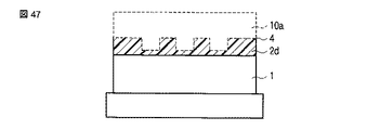
[図45]
被加工基板1上に1ショット分の光硬化性樹脂2dがインクジェット法により塗布され、その後、被加工基板1とモールド10aとの位置合わせが行われる。
[Fig. 45]
One shot of photo-
[図46]
光硬化性樹脂2dにモールド10aを接触させる。この時、被加工基板1の温度はモールド10aの融点(氷もしくはドライアイスの融点)未満に保たれていることが望ましい。これにより、モールド10aのパターン形状を所定の形状に容易に保持できる。モールド10aを介して光硬化性樹脂2dに光3を照射することにより、光硬化性樹脂2dを硬化させる。
[FIG. 46]
The
[図47]
被加工基板1を加熱することにより、モールド10aを融解する。モールド10aを直接加熱することにより、モールド10aを融解しても構わない。加熱温度はモールド10aの融点以上である。融解したモールド10a(液体)は、例えば、スピンドライ法により除去する。
[FIG. 47]
The
本実施形態によれば、光硬化性樹脂2dからモールド10を引っ張る必要がないので、離型欠陥は生じない。
According to the present embodiment, it is not necessary to pull the
なお、従来と同様に、光硬化性樹脂2dからモールド10を引っ張って、離型を行っても構わない。この場合、加熱によりモールド10aを多少融解し、光硬化性樹脂2dとモールド10との間の密着力を弱めた後に、離型を行うことにより、離型欠陥の発生を抑制できる。
Similarly to the conventional case, the
図48−図51を用いてモールド10aの形成方法の一例について説明する。
An example of a method for forming the
ここでは、モールド10aが氷で形成された場合について説明する。
Here, a case where the
[図48]
モールド10aの凹凸パターンを反転させた凹凸パターンを有する石英基板(親モールド)10a’を用意する。このような親モールドは、一般のフォトマスクを形成する場合と同様に、石英基板の表面をプラズマエッチングにより加工することにより得られる。
[FIG. 48]
A quartz substrate (parent mold) 10a ′ having a concavo-convex pattern obtained by inverting the concavo-convex pattern of the
[図49]
容器50の上方に、0℃以下に冷却された親モールド10a’を設置する。容器50は図示しない冷却機構により冷却できるようになっている。
[FIG. 49]
A
[図50]
容器50内に0℃付近に冷却された純水51を注入し、その後、親モールド10a’を容器50内の純水51中に所定の深さまで浸し、上記の図示しない冷却機構により容器50を冷却し、純水51を凍らせる。
[FIG. 50]
[図51]
容器50から親モールド10a’および凍らせた純水(氷)51を取り出し、氷51と親モールド10a’とを分離することで、モールド10aに相当する、氷51からなるモールド(子モールド)が得られる。
[FIG. 51]
The
モールド10aがドライアイスで形成された場合も同様の方法で、モールド10aを形成することができる。
Even when the
(第13の実施形態)
図52−図55は、第13の実施形態に係るインプリント方法を用いたパターン形成方法を示す断面図である。
(13th Embodiment)
52 to 55 are cross-sectional views showing a pattern forming method using the imprint method according to the thirteenth embodiment.
本実施形態が第1−第12の実施形態と異なる点は、光硬化性樹脂中に溶融させたガスを気化させることで、離型時にアウトガスを発生させることにある。 The present embodiment is different from the first to twelfth embodiments in that outgas is generated at the time of mold release by vaporizing a gas melted in the photocurable resin.
[図52]
液体の光硬化性樹脂2d(第6の光硬化性樹脂)を空気、窒素、二酸化炭素、He、NeまたはArなどのガスの高圧雰囲気60中に晒すことにより、光硬化性樹脂2d中にガス61を溶解させる。
[FIG. 52]
By exposing the liquid
[図53]
高圧雰囲気60中において、被加工基板1上にガス61が溶解された光硬化性樹脂2dが塗布される。塗布方法は、例えば、スピンコート法またはインクジェット法である。上記塗布方法とスキージとを組み合わせても構わない。この場合、所望の厚さを有する光硬化性樹脂2dを容易に形成することができる。
[FIG. 53]
In the high-
[図54]
高圧雰囲気60中において、光硬化性樹脂2dにモールド10を接触させ、その後、モールド10を介して光硬化性樹脂2dに光3を照射することにより、光硬化性樹脂2dを硬化させる。
[FIG. 54]
In the high-
[図55]
雰囲気を高圧雰囲気60から減圧雰囲気62に変える。その結果、光硬化性樹脂2d中に溶解されたガス61が気化し、光硬化性樹脂2dとモールド10との界面にガス61が溜まる。この界面に溜まったガス(アウトガス)61によって、光硬化性樹脂2とモールド10との間の密着力は弱まるので、従来よりも弱い力で、離型を行うことができる。したがって、離型欠陥の発生を抑制できるようになる。
[FIG. 55]
The atmosphere is changed from the
なお、本実施形態では、被加工基板1上の全てのショット領域に光硬化性樹脂2dを塗布する場合について説明したが、一部のショット領域、つまり、相対的に離型力が大きい領域(相対的に離型欠陥が発生しにくい領域))のみに光硬化性樹脂2dを塗布し、その他の相対的に離型力が小さい領域には通常の光硬化性樹脂(第7の光硬化性樹脂)を塗布しても構わない。すなわち、本実施形態は、前述した第10の実施形態や後述する第14または第15の実施形態のように、ショット領域(第1の領域、第2の領域)毎にガスを発生させるか否かを制御するインプリント方法に適用しても構わない。
In the present embodiment, the case where the
(第14の実施形態)
図56および図57は、第14の実施形態に係るインプリント方法を用いたパターン形成方法を示す断面図である。
(Fourteenth embodiment)
56 and 57 are cross-sectional views showing a pattern forming method using the imprint method according to the fourteenth embodiment.
[図56]
本実施形態では、2種類の光硬化性樹脂(第1および第2の光構成樹脂)2f,2gを用いる。
[FIG. 56]
In the present embodiment, two types of photocurable resins (first and second photoconstituting resins) 2f and 2g are used.
第1の光硬化性樹脂2f(第2の光硬化性樹脂)は、紫外線照射により、硬化およびガス発生を発現する。 The 1st photocurable resin 2f (2nd photocurable resin) expresses hardening and gas generation by ultraviolet irradiation.
第2の光硬化性樹脂2g(第3の光硬化性樹脂)は、紫外線照射により、硬化のみを発現する。
The 2nd
第1の光硬化性樹脂2fの材料は、例えば、光重合開始剤を添加したアクリルモノマーにDNQ(ナフトキノンジアジド)を結合させたベンゾフェノン化合物が添加されたものである。 The material of the first photocurable resin 2f is obtained, for example, by adding a benzophenone compound in which DNQ (naphthoquinonediazide) is bonded to an acrylic monomer to which a photopolymerization initiator is added.
第2の光硬化性樹脂2gは、例えば、光重合開始剤が添加されたアクリルモノマーである。
The second
2種類の各光硬化性樹脂2f,2gはそれぞれインプリント装置の薬液塗布装置内に設置した2つの独立した薬液ラインに供給できるようになっている。各薬液ラインの先端にはインクジェットノズルが設置されている。 Each of the two types of photocurable resins 2f and 2g can be supplied to two independent chemical liquid lines installed in the chemical liquid coating apparatus of the imprint apparatus. An inkjet nozzle is installed at the tip of each chemical line.
インプリント装置は、モールドのパターンのサイズに応じて適切な硬化樹脂分布と樹脂種を決定する。 The imprint apparatus determines an appropriate cured resin distribution and resin type according to the size of the mold pattern.
具体的には、微細なパターンが形成された領域に対しては第1の光硬化性樹脂2fを使用し、それ以外の領域に対しては第2の光硬化性樹脂2gを使用する。
Specifically, the first photocurable resin 2f is used for the region where the fine pattern is formed, and the second
微細なパターンが形成された領域(第1の領域)は、モールト゛と光硬化性樹脂の接触面積が大きいために離型力が大きいので、ガスを発生する第1の光硬化性樹脂2fを使用する。それ以外の領域(第2の領域)では離型力が相対的に小さいので、ガスを発生しない第2の光硬化性樹脂2gを使用する。
Since the area where the fine pattern is formed (first area) has a large release area due to the large contact area between the mold and the photocurable resin, the first photocurable resin 2f that generates gas is used. To do. In the other region (second region), the release force is relatively small, so the second
[図57]
光硬化性樹脂2f,2gにモールド10を接触させ、その後、モールド10を介して光硬化性樹脂2f,2gに光3(ここではUV光)を照射することにより、硬化性樹脂2f,2gを硬化させる。
[FIG. 57]
The
この時、光硬化性樹脂2f中のDNQが光3の照射によって分解され、光硬化性樹脂2fからはアウトガス(窒素ガス)4aが発生する。アウトガス4aは光硬化性樹脂2fとモールド10との間に溜まる。これにより、離型時における光硬化性樹脂2fとモールド10との間の密着力は弱くなり、離型欠陥の発生を抑制できるようになる。
At this time, DNQ in the photocurable resin 2f is decomposed by irradiation with
また、密着力が弱くなったことにより、離型時に、インプリント装置のモールド保持機構からモールド10が脱落することを防止できる。モールド10の脱落は、モールド10の破損を招く可能性がある。モールド10は高価であるため、脱落によるモールド10の破損を防ぐことは、製造コスト削減の点で重要である。
Further, since the adhesive force is weakened, it is possible to prevent the
なお、アウトガスはパターンの精度(形状、寸法)に与える影響が許容できる程度に発生量を調整してある。光硬化性樹脂2fで形成されたパターンは必要な精度内であることを確認した。 The amount of outgas is adjusted to such an extent that the influence on the pattern accuracy (shape and size) is acceptable. It was confirmed that the pattern formed with the photocurable resin 2f was within the required accuracy.
一方、光硬化性樹脂2gからはアウトガスは発生しない。したがって、光硬化性樹脂2gで形成されたパターンは高い精度を有する。
On the other hand, no outgas is generated from the
なお、図56、図57には、一つの微細なパターンが形成された領域(第1の領域)および一つのそれ以外の領域(第2の領域)しか示していないが、実際には複数の第1の領域および複数の第2の領域に対してそれぞれについて図56、図57に示した工程を行う。以下に説明する変形例についても同様である。 Note that FIGS. 56 and 57 show only a region (first region) where one fine pattern is formed and one other region (second region). The processes shown in FIGS. 56 and 57 are performed on the first region and the plurality of second regions, respectively. The same applies to the modifications described below.
図58に、本実施形態の変形例を示す。本実施形態では、被加工基板1上に光硬化性樹脂2f,2gを塗布したが、この変形例では、モールド10のパターン面上に光硬化性樹脂2f,2gを塗布する。次に、光硬化性樹脂2f,2g上に被加工基板11を設置し、モールド10を介して光硬化性樹脂2f,2gに光3を照射する。この後は、離型等の周知の工程が行われる。この変形例(モールドに光硬化性樹脂を塗布する例)は、既に述べた第13の実施形態等の実施形態、後で述べる第15の実施形態等の実施形態に対しても同様に実施可能である。
FIG. 58 shows a modification of this embodiment. In this embodiment, the photocurable resins 2f and 2g are applied on the
(第15の実施形態)
図59は、第15の実施形態に係るインプリント方法を用いたパターン形成方法を示す断面図である。
(Fifteenth embodiment)
FIG. 59 is a cross-sectional view showing a pattern forming method using the imprint method according to the fifteenth embodiment.
[図59]
本実施形態が第14の実施形態と異なる点は、パターン密度が高い領域(密パターン領域)に対しては第1の光硬化性樹脂2fを使用し、パターン密度が低い領域(疎パターン領域)に対しては第2の光硬化性樹脂2gを使用することにある。
[FIG. 59]
The difference between the present embodiment and the fourteenth embodiment is that the first photocurable resin 2f is used for a region having a high pattern density (dense pattern region), and a region having a low pattern density (sparse pattern region). Is to use 2 g of the second photocurable resin.
密パターン領域は、例えば、1:1のL/Sパターンが形成された領域である。密パターン領域は、モールト゛と光硬化性樹脂の接触面積が大きく離型力が大きいので、密パターン領域に対してはガスを発生する第1の光硬化性樹脂2fを使用する。 The dense pattern region is, for example, a region where a 1: 1 L / S pattern is formed. In the dense pattern region, the contact area between the mold and the photocurable resin is large, and the release force is large. Therefore, the first photocurable resin 2f that generates gas is used for the dense pattern region.
疎パターン領域は、例えば、孤立ライン(孤立スペース)やコンタクトホールが形成された領域である。疎パターン領域は離型力が大きくないので、疎パターン領域に対してはガスを発生しない第2の光硬化性樹脂2gを使用する。
The sparse pattern region is, for example, a region where an isolated line (isolated space) or contact hole is formed. Since the release force is not large in the sparse pattern region, the second
光硬化性樹脂2f,2gにモールド10を接触させ、その後、モールド10を介して光硬化性樹脂2f,2gに光3(ここではUV光)を照射することにより、硬化性樹脂2f,2gを硬化させる。
The
この時、光硬化性樹脂2fからアウトガス(窒素ガス)4aが発生し、密パターン領域での密着力は弱くなる。これにより、離型時に、インプリント装置のモールド保持機構からモールド10が脱落することを防止できる。
At this time, outgas (nitrogen gas) 4a is generated from the photocurable resin 2f, and the adhesion in the dense pattern region is weakened. Thereby, the
また、離型後の光硬化性樹脂2f,2gからなるパターン(インプリントパターン)の欠陥を検査したところ、従来に比べて、離型欠陥が低減していることが分かった。その理由は以下のように考えられる。
Moreover, when the defect of the pattern (imprint pattern) which consists of
密パターン領域での密着力が弱くなることで、密パターン領域と疎パターン領域との間での離型力の差は小さくなる。その結果、離型時におけるモールド10のパターン面内に発生する応力は小さくなり、離型欠陥の発生原因となる、モールド10のパターン面の形状変化は抑制される。
As the adhesion force in the dense pattern region becomes weak, the difference in the release force between the dense pattern region and the sparse pattern region becomes small. As a result, the stress generated in the pattern surface of the
(第16の実施形態)
図60および図61は、第16の実施形態に係るインプリント方法を用いたパターン形成方法を示す断面図である。
(Sixteenth embodiment)
60 and 61 are cross-sectional views showing a pattern forming method using the imprint method according to the sixteenth embodiment.
[図60]
第3の実施形態と同様に、光硬化性樹脂2aの塗布工程からインプリント工程までの工程(図17,図18)が行われ、その後、モールド10を介して光硬化性樹脂2aに第1の光3aが照射される。
[FIG. 60]
Similarly to the third embodiment, the steps from the
第1の光3aは可視光に相当する波長を中心波長とする。第1の光3aの光源は、例えば、高出力のキセノンランプである。第1の光3aの照射によって光硬化性樹脂2aは光硬化反応を起こし固まる。
The
この時、ナフトキノンジアジド化合物は可視光ではあまり分解されないので、光硬化性樹脂2aからアウトガスは放出されない。したがって、光硬化性樹脂2a内に気泡ができることはない。
At this time, since the naphthoquinonediazide compound is not decomposed so much by visible light, no outgas is released from the
[図61]
モールド10を介して光硬化性樹脂2aに第2の光3bが照射される。
[FIG. 61]
The
第2の光3bは紫外線であり、その中心波長は、例えば、365nmである。第2の光3aの光源は、例えば、水銀ランプである。第2の光3bによって、ナフトキノンジアジドはインデンカルボン酸に高効率で分解され、その結果として、光硬化性樹脂2aからアウトガス(ここでは窒素ガス)4が放出される。したがって、本実施形態でも第3の実施形態と同様に、離型欠陥の発生を抑制できる。
The
この時、窒素ガスは固化した光硬化性樹脂2a中では固体の圧力によって圧縮されるので、光硬化性樹脂2aの内部に窒素ガスの空隙ができることはない。光硬化性樹脂2aの表面付近で発生した窒素ガスのみがアウトガス4として放出される。
At this time, since the nitrogen gas is compressed by the solid pressure in the solidified
(第17の実施形態)
図62および図63は、第17の実施形態に係るインプリント方法を用いたパターン形成方法を示す断面図である。
(Seventeenth embodiment)
62 and 63 are sectional views showing a pattern forming method using the imprint method according to the seventeenth embodiment.
[図62]
第2の実施形態と同様に、光硬化性樹脂2の塗布工程からインプリント工程までの工程(図12,図13)が行われ、その後、モールド10を介して光硬化性樹脂2に第1の光3aが照射される。第1の光3aの光源は、第16の実施形態と同様に、高出力のキセノンランプである。
[FIG. 62]
As in the second embodiment, the steps from the
[図63]
モールド10を介して光硬化性樹脂2に第2の光3bが照射される。
[FIG. 63]
The
第2の光3bは、波長400nm以下の紫外線である。第2の光3bの光源は、第16の実施形態と同様に、水銀ランプである。
The
この時、第2の光3bの照射により光触媒層11は触媒作用を発現し、光触媒層11と接触している部分の光硬化性樹脂2の表面が分解され、光硬化性樹脂2の表面からアウトガス4が発生する。したがって、本実施形態でも第2の実施形態と同様に、離型欠陥の発生を抑制できる。
At this time, the
なお、本発明は上記実施形態そのままに限定されるものではなく、実施段階ではその要旨を逸脱しない範囲で構成要素を変形して具体化できる。また、上記実施形態に開示されている複数の構成要素の適宜な組み合わせにより、種々の発明を形成できる。例えば、実施形態に示される全構成要素から幾つかの構成要素を削除してもよい。具体的には、第10の実施形態と第14の実施形態と第15の実施形態とを適宜組み合わせても構わない。 Note that the present invention is not limited to the above-described embodiment as it is, and can be embodied by modifying the constituent elements without departing from the scope of the invention in the implementation stage. In addition, various inventions can be formed by appropriately combining a plurality of components disclosed in the embodiment. For example, some components may be deleted from all the components shown in the embodiment. Specifically, the tenth embodiment, the fourteenth embodiment, and the fifteenth embodiment may be appropriately combined.
さらに、異なる実施形態にわたる構成要素を適宜組み合わせてもよい。 Furthermore, constituent elements over different embodiments may be appropriately combined.
その他、本発明の要旨を逸脱しない範囲で、種々変形して実施できる。 In addition, various modifications can be made without departing from the scope of the present invention.
1…被加工基板、2,2a,2d,2e,2f,2g…光硬化性樹脂、2b…ナフトキノンジアジド化合物を含まない光硬化性樹脂(第1の光硬化性樹脂)、2c…ナフトキノンジアジド化合物を含む光硬化性樹脂(第2の光硬化性樹脂)、3,3a,3b…光、4,4a…アウトガス、5…半透明膜、10,10a…モールド、10a’…親モールド、11…光触媒層、12…熱発生部材、13…被膜、14…位相/透過率調整膜、15…光源、16…反射ミラー、20…スキャンノズル、30…チャック、31…配管、40…容器、41…液体、50…容器、51…純水、R1…離型力が大きい領域(第1の領域)、R2…離型力が小さい領域(第2の領域)、60…高圧雰囲気、61…ガス、62…減圧雰囲気。
DESCRIPTION OF
Claims (17)
前記光硬化性樹脂にインプリント用モールドを接触させること、
前記インプリント用モールドを介して前記光硬化性樹脂に光を照射することにより、前記光硬化性樹脂を硬化すること、
少なくとも前記第1の領域を含む前記被加工基板の領域上に塗布された前記光硬化性樹脂に所定の処理を加えることによりガスを発生させること、前記第1の領域に塗布された前記光硬化性樹脂から発生する前記ガスの発生量は、前記第2の領域に塗布された前記光硬化性樹脂から発生する前記ガスの発生量よりも多いこと、および
前記ガスの発生後、前記光硬化性樹脂から前記インプリント用モールドを離し、前記被加工基板上にパターンを形成することを含み、
前記第1の領域は前記第2の領域よりも密度が高いパターンが形成される領域、または、前記第1の領域は前記第2の領域よりもサイズが大きいパターンが形成される領域であることを特徴とするインプリント方法。 Applying a photocurable resin on the substrate to be processed including the first region and the second region;
Bringing an imprint mold into contact with the photocurable resin;
Curing the photocurable resin by irradiating the photocurable resin with light through the imprint mold,
Generating a gas by applying a predetermined treatment to the photocurable resin applied on the region of the substrate to be processed including at least the first region; and the photocuring applied to the first region. The amount of the gas generated from the curable resin is larger than the amount of the gas generated from the photocurable resin applied to the second region, and after the generation of the gas, the photocurable property releasing the imprint mold from the resin, see contains to form a pattern on the processed substrate,
The first region is a region where a pattern having a higher density than the second region is formed, or the first region is a region where a pattern having a size larger than that of the second region is formed. An imprint method characterized by the above.
前記被加工基板上に前記光硬化性樹脂を塗布することにおいて、前記第1および第2の領域上に前記第1の光硬化性樹脂を塗布し、および
前記ガスを発生させるための前記所定の処理は、
前記第1および第2の領域上の前記第1の光硬化性樹脂それぞれに対して、異なる照射量で光を照射すること、
前記第1および第2の領域上の前記第1の光硬化性樹脂それぞれに対して、異なる照射量で異なる熱量で加熱すること、および、
前記第1および第2の領域上の前記第1の光硬化性樹脂それぞれに対して、異なる照射量で異なる圧力を加えることのいずれかを含むことを特徴とする請求項1に記載のインプリント方法。 The photocurable resin that generates gas by the predetermined treatment is a first photocurable resin in which the amount of gas generated changes according to any of the light irradiation amount, the heating amount, and the pressure,
In applying the photocurable resin on the substrate to be processed, the first photocurable resin is applied on the first and second regions, and the predetermined gas for generating the gas is applied. Processing is
Irradiating each of the first photocurable resins on the first and second regions with different doses;
Heating each of the first photocurable resins on the first and second regions with different doses and different amounts of heat; and
2. The imprint according to claim 1, further comprising: applying different pressures with different irradiation amounts to the first photocurable resins on the first and second regions, respectively. Method.
前記第1の領域上に光照射、加熱および減圧のいずれかの処理によりガスを発生する光硬化性樹脂を塗布すること、前記第2の領域上に光照射、加熱および減圧のいずれの処理によってもガスを発生しない光硬化性樹脂を塗布することを含み、
前記ガスを発生させることは、前記第1の領域上の前記光硬化性樹脂に光照射、加熱および減圧のいずれかの処理を施すことによりガスを発生することを含むことを特徴とする請求項1に記載のインプリント方法。 Applying the photocurable resin,
Applying a photocurable resin that generates gas by any one of light irradiation, heating, and pressure reduction on the first region, and applying light irradiation, heating, and pressure reduction on the second region. Including applying a photocurable resin that does not generate gas,
The generating of the gas includes generating the gas by subjecting the photocurable resin on the first region to any one of light irradiation, heating, and decompression. 2. The imprint method according to 1.
Priority Applications (3)
| Application Number | Priority Date | Filing Date | Title |
|---|---|---|---|
| JP2009061650A JP4892025B2 (en) | 2008-09-26 | 2009-03-13 | Imprint method |
| US12/563,461 US8419995B2 (en) | 2008-09-26 | 2009-09-21 | Imprint method |
| KR1020090090940A KR101129770B1 (en) | 2008-09-26 | 2009-09-25 | Imprint method |
Applications Claiming Priority (3)
| Application Number | Priority Date | Filing Date | Title |
|---|---|---|---|
| JP2008249167 | 2008-09-26 | ||
| JP2008249167 | 2008-09-26 | ||
| JP2009061650A JP4892025B2 (en) | 2008-09-26 | 2009-03-13 | Imprint method |
Publications (3)
| Publication Number | Publication Date |
|---|---|
| JP2010103464A JP2010103464A (en) | 2010-05-06 |
| JP2010103464A5 JP2010103464A5 (en) | 2011-06-23 |
| JP4892025B2 true JP4892025B2 (en) | 2012-03-07 |
Family
ID=42056548
Family Applications (1)
| Application Number | Title | Priority Date | Filing Date |
|---|---|---|---|
| JP2009061650A Expired - Fee Related JP4892025B2 (en) | 2008-09-26 | 2009-03-13 | Imprint method |
Country Status (3)
| Country | Link |
|---|---|
| US (1) | US8419995B2 (en) |
| JP (1) | JP4892025B2 (en) |
| KR (1) | KR101129770B1 (en) |
Families Citing this family (33)
| Publication number | Priority date | Publication date | Assignee | Title |
|---|---|---|---|---|
| KR101522977B1 (en) * | 2007-04-23 | 2015-05-28 | 난창 오-필름 옵토일렉트로닉스 테크놀로지 리미티드 | Mass production of micro-optical devices, corresponding tools, and resultant structures |
| US8237133B2 (en) * | 2008-10-10 | 2012-08-07 | Molecular Imprints, Inc. | Energy sources for curing in an imprint lithography system |
| JP2010182824A (en) * | 2009-02-04 | 2010-08-19 | Toshiba Corp | Method of manufacturing magnetic random access memory, and method of manufacturing embedded memory |
| JP5175771B2 (en) * | 2009-02-27 | 2013-04-03 | 株式会社日立ハイテクノロジーズ | Fine structure transfer apparatus and fine structure transfer method |
| JP4881403B2 (en) * | 2009-03-26 | 2012-02-22 | 株式会社東芝 | Pattern formation method |
| JP5446434B2 (en) * | 2009-04-30 | 2014-03-19 | Jsr株式会社 | Curable composition for nanoimprint lithography and nanoimprint method |
| JP5295870B2 (en) * | 2009-06-02 | 2013-09-18 | 株式会社東芝 | Imprint pattern forming method |
| JP2011009641A (en) * | 2009-06-29 | 2011-01-13 | Toshiba Corp | Method of manufacturing semiconductor device, and template for imprint |
| US20120025426A1 (en) * | 2010-07-30 | 2012-02-02 | Seagate Technology Llc | Method and system for thermal imprint lithography |
| FR2969772B1 (en) * | 2010-12-22 | 2012-12-28 | Commissariat Energie Atomique | METHOD OF NANO PRINTING LITHOGRAPHY |
| EP2690650B1 (en) * | 2011-06-23 | 2017-08-09 | Asahi Kasei Kabushiki Kaisha | Laminate for forming fine pattern, and method for producing laminate for forming fine pattern |
| JP5315513B2 (en) | 2011-07-12 | 2013-10-16 | 丸文株式会社 | Light emitting device and manufacturing method thereof |
| JP5686779B2 (en) * | 2011-10-14 | 2015-03-18 | キヤノン株式会社 | Imprint apparatus and article manufacturing method using the same |
| JP6012344B2 (en) * | 2011-10-24 | 2016-10-25 | キヤノン株式会社 | Method for forming film |
| JP5854795B2 (en) * | 2011-11-28 | 2016-02-09 | キヤノン株式会社 | Pattern formation method |
| JP5804915B2 (en) | 2011-11-28 | 2015-11-04 | キヤノン株式会社 | Curable composition and pattern forming method |
| JP5971938B2 (en) * | 2011-12-19 | 2016-08-17 | キヤノン株式会社 | Method for producing cured product and pattern forming method |
| JP5868215B2 (en) * | 2012-02-27 | 2016-02-24 | キヤノン株式会社 | Imprint apparatus, imprint method, and article manufacturing method using the same |
| JP6000712B2 (en) | 2012-07-24 | 2016-10-05 | キヤノン株式会社 | Resin manufacturing method and resin manufacturing apparatus |
| US9863883B2 (en) | 2012-08-10 | 2018-01-09 | Hamamatsu Photonics K.K. | Surface-enhanced raman scattering element |
| EP2884264B1 (en) | 2012-08-10 | 2019-11-20 | Hamamatsu Photonics K.K. | Surface-enhanced raman scattering element, and method for producing same |
| JP6058313B2 (en) * | 2012-08-10 | 2017-01-11 | 浜松ホトニクス株式会社 | Surface-enhanced Raman scattering unit |
| JP6278645B2 (en) * | 2012-09-24 | 2018-02-14 | キヤノン株式会社 | Photocurable composition and method for producing film using the same |
| TWI589994B (en) * | 2012-10-09 | 2017-07-01 | 佳能股份有限公司 | Photocurable composition and method for manufacturing film |
| KR101426463B1 (en) * | 2012-12-21 | 2014-08-06 | (주) 에이와케이 | Apparatus for manufacturing film used micro size pattern and method using the same |
| CN105283968A (en) | 2013-07-17 | 2016-01-27 | 丸文株式会社 | Semiconductor light-emitting element and production method |
| US9082625B2 (en) * | 2013-12-11 | 2015-07-14 | International Business Machines Corporation | Patterning through imprinting |
| JP5757512B1 (en) * | 2014-03-06 | 2015-07-29 | 丸文株式会社 | Deep ultraviolet LED and manufacturing method thereof |
| CN107075661B (en) * | 2014-09-26 | 2020-03-17 | 韩国机械研究院 | Substrate formed with a plurality of nanogaps and method for preparing the same |
| US9929317B2 (en) | 2015-01-16 | 2018-03-27 | Marubun Corporation | Deep ultraviolet LED and method for manufacturing the same |
| JP6230038B2 (en) | 2015-09-03 | 2017-11-15 | 丸文株式会社 | Deep ultraviolet LED and manufacturing method thereof |
| KR101811819B1 (en) | 2016-03-30 | 2017-12-22 | 마루분 가부시키가이샤 | Deep ultraviolet LED and method for manufacturing the same |
| JP7316610B6 (en) | 2018-01-26 | 2024-02-19 | 丸文株式会社 | Deep ultraviolet LED and its manufacturing method |
Family Cites Families (25)
| Publication number | Priority date | Publication date | Assignee | Title |
|---|---|---|---|---|
| FR1580370A (en) * | 1968-07-01 | 1969-09-05 | ||
| US6671034B1 (en) * | 1998-04-30 | 2003-12-30 | Ebara Corporation | Microfabrication of pattern imprinting |
| US6218316B1 (en) * | 1998-10-22 | 2001-04-17 | Micron Technology, Inc. | Planarization of non-planar surfaces in device fabrication |
| JP2000194142A (en) | 1998-12-25 | 2000-07-14 | Fujitsu Ltd | Pattern forming method and production of semiconductor device |
| US20080164638A1 (en) | 2006-11-28 | 2008-07-10 | Wei Zhang | Method and apparatus for rapid imprint lithography |
| KR20050026088A (en) * | 2002-08-01 | 2005-03-14 | 몰레큘러 임프린츠 인코퍼레이티드 | Scatterometry alignment for imprint lithography |
| US7070405B2 (en) * | 2002-08-01 | 2006-07-04 | Molecular Imprints, Inc. | Alignment systems for imprint lithography |
| US7374864B2 (en) * | 2003-02-13 | 2008-05-20 | The Regents Of The University Of Michigan | Combined nanoimprinting and photolithography for micro and nano devices fabrication |
| JP4651390B2 (en) * | 2003-03-27 | 2011-03-16 | コリア・インスティテュート・オブ・マシナリー・アンド・マテリアルズ | UV nanoimprint lithography using multiple relief element stamps |
| JP2005064143A (en) * | 2003-08-08 | 2005-03-10 | Seiko Epson Corp | Method of forming resist pattern, method of forming wiring pattern, method of manufacturing semiconductor device, electrooptic device, and electronic equipment |
| US8097400B2 (en) * | 2005-02-22 | 2012-01-17 | Hewlett-Packard Development Company, L.P. | Method for forming an electronic device |
| US7611348B2 (en) | 2005-04-19 | 2009-11-03 | Asml Netherlands B.V. | Imprint lithography |
| JP4290177B2 (en) * | 2005-06-08 | 2009-07-01 | キヤノン株式会社 | Mold, alignment method, pattern forming apparatus, pattern transfer apparatus, and chip manufacturing method |
| US7482280B2 (en) * | 2005-08-15 | 2009-01-27 | Taiwan Semiconductor Manufacturing Company, Ltd. | Method for forming a lithography pattern |
| US7488771B2 (en) * | 2005-09-02 | 2009-02-10 | International Business Machines Corporation | Stabilization of vinyl ether materials |
| US8011916B2 (en) * | 2005-09-06 | 2011-09-06 | Canon Kabushiki Kaisha | Mold, imprint apparatus, and process for producing structure |
| TWI283631B (en) * | 2005-10-25 | 2007-07-11 | Ind Tech Res Inst | Method and device for demolding |
| US20070267764A1 (en) * | 2005-10-25 | 2007-11-22 | Dai Nippon Printing Co., Ltd. | Mold for photocuring nano-imprint and its fabrication process |
| JP4267631B2 (en) | 2006-02-13 | 2009-05-27 | トヨタ自動車株式会社 | Message data processing device |
| JP5309436B2 (en) | 2006-10-16 | 2013-10-09 | 日立化成株式会社 | Resin microstructure, method for producing the same, and polymerizable resin composition |
| KR101371093B1 (en) * | 2006-11-03 | 2014-03-10 | 엘아이지에이디피 주식회사 | Apparatus for forming a nano-pattern and method using the same |
| JP5211505B2 (en) * | 2007-02-21 | 2013-06-12 | 凸版印刷株式会社 | Imprint mold, imprint mold manufacturing method, and optical imprint method |
| JP5137635B2 (en) | 2007-03-16 | 2013-02-06 | キヤノン株式会社 | Imprint method, chip manufacturing method, and imprint apparatus |
| KR100829398B1 (en) | 2007-05-17 | 2008-05-15 | 주식회사 에이디피엔지니어링 | Apparatus for inspection stamp and method for forming a nano-pattern |
| WO2010005032A1 (en) * | 2008-07-09 | 2010-01-14 | 東洋合成工業株式会社 | Pattern-forming method |
-
2009
- 2009-03-13 JP JP2009061650A patent/JP4892025B2/en not_active Expired - Fee Related
- 2009-09-21 US US12/563,461 patent/US8419995B2/en not_active Expired - Fee Related
- 2009-09-25 KR KR1020090090940A patent/KR101129770B1/en active IP Right Grant
Also Published As
| Publication number | Publication date |
|---|---|
| KR101129770B1 (en) | 2012-03-23 |
| US20100078860A1 (en) | 2010-04-01 |
| JP2010103464A (en) | 2010-05-06 |
| US8419995B2 (en) | 2013-04-16 |
| KR20100035617A (en) | 2010-04-05 |
Similar Documents
| Publication | Publication Date | Title |
|---|---|---|
| JP4892025B2 (en) | Imprint method | |
| JP2008091782A (en) | Pattern forming template, pattern forming method and nano-imprinter | |
| JP5100609B2 (en) | Manufacturing method of semiconductor device | |
| JP2010103464A5 (en) | ||
| JP5499668B2 (en) | Imprint mold and pattern forming method using the mold | |
| JP2004304097A (en) | Pattern forming method, and manufacturing method for semiconductor device | |
| JP2010149482A (en) | Mold for inprint and pattern forming method | |
| JP2008078550A (en) | Imprint mold, its manufacturing method, and pattern formation method | |
| US9028639B2 (en) | Method of manufacturing stamp for plasmonic nanolithography apparatus and plasmonic nanolithography apparatus | |
| JP5537400B2 (en) | Pattern forming method and apparatus | |
| JP4937500B2 (en) | Imprint method | |
| JP2010258182A (en) | Method and device for micropattern transfer | |
| JP2005286222A (en) | Imprinting stamper, manufacturing method of the imprinting stamper, imprint method, and disassembling method of the imprinting stamper | |
| JP5568960B2 (en) | Pattern formation method by nanoimprint | |
| JP5397054B2 (en) | Nanoimprint method and nanoimprint apparatus | |
| JP2008119870A (en) | Imprinting mold | |
| JP5082262B2 (en) | Manufacturing method of resin film | |
| JP5574802B2 (en) | Manufacturing method of structure | |
| JP2007200422A (en) | Manufacturing method of patterned magnetic recording medium | |
| JP5644906B2 (en) | Nanoimprint method | |
| JP2020170863A (en) | Imprint mold | |
| JP2011014875A5 (en) | ||
| JP5481438B2 (en) | Imprint mold and pattern forming method | |
| JP4858030B2 (en) | Imprint mold, imprint mold manufacturing method, and pattern forming method | |
| JP6036865B2 (en) | Imprint mold |
Legal Events
| Date | Code | Title | Description |
|---|---|---|---|
| A521 | Written amendment |
Free format text: JAPANESE INTERMEDIATE CODE: A523 Effective date: 20110502 |
|
| A621 | Written request for application examination |
Free format text: JAPANESE INTERMEDIATE CODE: A621 Effective date: 20110502 |
|
| A871 | Explanation of circumstances concerning accelerated examination |
Free format text: JAPANESE INTERMEDIATE CODE: A871 Effective date: 20110502 |
|
| A975 | Report on accelerated examination |
Free format text: JAPANESE INTERMEDIATE CODE: A971005 Effective date: 20110527 |
|
| A131 | Notification of reasons for refusal |
Free format text: JAPANESE INTERMEDIATE CODE: A131 Effective date: 20110607 |
|
| A521 | Written amendment |
Free format text: JAPANESE INTERMEDIATE CODE: A523 Effective date: 20110808 |
|
| TRDD | Decision of grant or rejection written | ||
| A01 | Written decision to grant a patent or to grant a registration (utility model) |
Free format text: JAPANESE INTERMEDIATE CODE: A01 Effective date: 20111122 |
|
| A01 | Written decision to grant a patent or to grant a registration (utility model) |
Free format text: JAPANESE INTERMEDIATE CODE: A01 |
|
| A61 | First payment of annual fees (during grant procedure) |
Free format text: JAPANESE INTERMEDIATE CODE: A61 Effective date: 20111216 |
|
| R151 | Written notification of patent or utility model registration |
Ref document number: 4892025 Country of ref document: JP Free format text: JAPANESE INTERMEDIATE CODE: R151 |
|
| FPAY | Renewal fee payment (event date is renewal date of database) |
Free format text: PAYMENT UNTIL: 20141222 Year of fee payment: 3 |
|
| S111 | Request for change of ownership or part of ownership |
Free format text: JAPANESE INTERMEDIATE CODE: R313111 |
|
| R350 | Written notification of registration of transfer |
Free format text: JAPANESE INTERMEDIATE CODE: R350 |
|
| LAPS | Cancellation because of no payment of annual fees |