JP4880436B2 - Semiconductor integrated circuit and power supply device - Google Patents
Semiconductor integrated circuit and power supply device Download PDFInfo
- Publication number
- JP4880436B2 JP4880436B2 JP2006329378A JP2006329378A JP4880436B2 JP 4880436 B2 JP4880436 B2 JP 4880436B2 JP 2006329378 A JP2006329378 A JP 2006329378A JP 2006329378 A JP2006329378 A JP 2006329378A JP 4880436 B2 JP4880436 B2 JP 4880436B2
- Authority
- JP
- Japan
- Prior art keywords
- transistor
- fet
- channel mos
- circuit
- mos transistor
- Prior art date
- Legal status (The legal status is an assumption and is not a legal conclusion. Google has not performed a legal analysis and makes no representation as to the accuracy of the status listed.)
- Expired - Fee Related
Links
Images
Classifications
-
- H—ELECTRICITY
- H03—ELECTRONIC CIRCUITRY
- H03K—PULSE TECHNIQUE
- H03K5/00—Manipulating of pulses not covered by one of the other main groups of this subclass
- H03K5/15—Arrangements in which pulses are delivered at different times at several outputs, i.e. pulse distributors
- H03K5/151—Arrangements in which pulses are delivered at different times at several outputs, i.e. pulse distributors with two complementary outputs
Landscapes
- Physics & Mathematics (AREA)
- Nonlinear Science (AREA)
- Semiconductor Integrated Circuits (AREA)
- Electronic Switches (AREA)
- Power Conversion In General (AREA)
Description
本発明は、半導体集積回路および電源装置に関し、特に、外部のFETを駆動する半導体集積回路および電源装置に関する。 The present invention relates to a semiconductor integrated circuit and a power supply device, and more particularly to a semiconductor integrated circuit and a power supply device for driving an external FET.
外部FET(Field Effect Transistor)を駆動するためのFET駆動回路が開発されている。たとえば、特許文献1〜3には、トランジスタをスイッチング制御する駆動回路が開示されている。
ところで、上記のような従来の駆動回路は、外部FETのオン状態およびオフ状態を切り替えるスイッチング制御回路を備え、スイッチング制御回路は、たとえばNチャネルMOS(Metal Oxide Semiconductor)トランジスタおよびPチャネルMOSトランジスタを組み合わせた回路が採用される。 By the way, the conventional driving circuit as described above includes a switching control circuit for switching the on-state and off-state of the external FET, and the switching control circuit combines, for example, an N-channel MOS (Metal Oxide Semiconductor) transistor and a P-channel MOS transistor. Circuit is adopted.
そして、FET駆動回路が集積化されたFET駆動IC(Integrated Circuit)では、外部端子がショートする等の異常が発生した場合、外部FETに大電流が流れて外部FETまたは外部FETの次段の回路が破壊されることを防ぐため、スイッチング制御回路におけるNチャネルMOSトランジスタおよびPチャネルMOSトランジスタのいずれか一方をオン状態とし、かつ他方をオフ状態として外部FETをオフ状態とする制御が行なわれる場合がある。 In an FET drive IC (Integrated Circuit) in which an FET drive circuit is integrated, when an abnormality such as a short-circuit of an external terminal occurs, a large current flows through the external FET and the external FET or a circuit subsequent to the external FET. In some cases, control is performed such that one of the N-channel MOS transistor and the P-channel MOS transistor in the switching control circuit is turned on, and the other FET is turned off and the external FET is turned off. is there.
しかしながら、スイッチング制御回路の出力が接続される外部端子が接地電位または電源電位等とショートした場合には、外部FETをオフ状態とすることができても、スイッチング制御回路におけるオン状態のMOSトランジスタに大電流が流れて破壊されてしまう場合がある。 However, if the external terminal to which the output of the switching control circuit is connected is short-circuited to the ground potential or the power supply potential, the external FET can be turned off, but the on-state MOS transistor in the switching control circuit can be turned off. A large current may flow and be destroyed.
このような問題点を解決するために、異常が発生した場合にはスイッチング制御回路におけるNチャネルMOSトランジスタおよびPチャネルMOSトランジスタの両方をオフ状態とし、かつ外部FETのゲートに外部FETがオフ状態となるようなバイアス電圧を供給するプルダウン抵抗またはプルアップ抵抗を備える構成が考えられる。しかしながら、このような構成では、外部FETの寄生容量、および通常数10kΩを有するプルアップ抵抗またはプルダウン抵抗に起因して、外部FETのゲートの電位をオン状態に対応する電位からオフ状態に対応する電位に遷移させるまでに要する時間が長くなってしまい、外部FETまたは外部FETの次段の回路が破壊される場合がある。 In order to solve such a problem, when an abnormality occurs, both the N-channel MOS transistor and the P-channel MOS transistor in the switching control circuit are turned off, and the external FET is turned off at the gate of the external FET. A configuration including a pull-down resistor or a pull-up resistor for supplying such a bias voltage is conceivable. However, in such a configuration, due to the parasitic capacitance of the external FET and the pull-up resistor or pull-down resistor that normally has several tens of kΩ, the potential of the gate of the external FET corresponds to the off state from the potential corresponding to the on state. The time required to make the transition to the potential becomes long, and the external FET or the circuit subsequent to the external FET may be destroyed.
それゆえに、本発明の目的は、外部FETおよび外部FETを駆動する回路の両方を保護することが可能な半導体集積回路および電源装置を提供することである。 SUMMARY OF THE INVENTION Therefore, an object of the present invention is to provide a semiconductor integrated circuit and a power supply device that can protect both an external FET and a circuit that drives the external FET.
上記課題を解決するために、本発明のある局面に係わる半導体集積回路は、外部のFETを駆動する半導体集積回路であって、FETに結合される第1のトランジスタおよび第2のトランジスタを含み、第1のトランジスタおよび第2のトランジスタの各々をオン・オフすることによりFETをオン・オフするスイッチング制御回路を備え、FETは、第1のトランジスタがオン状態であり、かつ第2のトランジスタがオフ状態のときにオフ状態となり、半導体集積回路は、さらに、第1のトランジスタおよび第2のトランジスタがオフ状態の場合、FETをオフするためのバイアス電圧をFETに供給するバイアス回路と、異常が検出された場合には、第1のトランジスタをオンし、かつ第2のトランジスタをオフすることによりFETをオフし、所定時間経過後、第1のトランジスタおよび第2のトランジスタをオフする保護制御回路とを備える。 In order to solve the above problems, a semiconductor integrated circuit according to an aspect of the present invention is a semiconductor integrated circuit that drives an external FET, and includes a first transistor and a second transistor coupled to the FET, a switching control circuit Ru on Ofusu the FET by turning on and off each of the first transistor and the second transistor, FET is a first transistor is turned on, and the second transistor When the first transistor and the second transistor are in the off state , the semiconductor integrated circuit further includes a bias circuit that supplies the FET with a bias voltage for turning off the FET. when detected, the FET by the first transistor turned on, and turns off the second transistor It was off, and a protection control circuit for turning off after a predetermined time has elapsed, the first transistor and the second transistor.
好ましくは、第1のトランジスタは、第1の導通電極が第1の固定電位に結合され、第2の導通電極がFETの制御電極に結合され、第2のトランジスタは、第1の導通電極がFETの制御電極に結合され、第2の導通電極が第2の固定電位に結合され、バイアス回路は、第1端が第1の固定電位に結合され、第2端がFETの制御電極に結合される抵抗を含み、FETは、制御電極の電位が第1の固定電位となったときにオフする。 Preferably, the first transistor has a first conduction electrode coupled to the first fixed potential, a second conduction electrode coupled to the control electrode of the FET, and the second transistor comprises a first conduction electrode Coupled to the control electrode of the FET, the second conducting electrode is coupled to the second fixed potential, and the bias circuit has a first end coupled to the first fixed potential and a second end coupled to the control electrode of the FET The FET is turned off when the potential of the control electrode becomes the first fixed potential.
上記課題を解決するために、本発明のある局面に係わる電源装置は、FETと、半導体集積回路とを備え、半導体集積回路は、FETに結合される第1のトランジスタおよび第2のトランジスタを有し、第1のトランジスタおよび第2のトランジスタの各々をオン・オフすることによりFETをオン・オフするスイッチング制御回路を含み、FETは、第1のトランジスタがオン状態であり、かつ第2のトランジスタがオフ状態のときにオフ状態となり、半導体集積回路は、さらに、第1のトランジスタおよび第2のトランジスタがオフ状態の場合、FETをオフするためのバイアス電圧をFETに供給するバイアス回路と、異常が検出された場合には、第1のトランジスタをオンし、かつ第2のトランジスタをオフすることによりFETをオフし、所定時間経過後、第1のトランジスタおよび第2のトランジスタをオフする保護制御回路とを含む。 In order to solve the above problems, a power supply device according to one aspect of the present invention comprises a FET, and a semiconductor integrated circuit, the semiconductor integrated circuit, have a first transistor and a second transistor coupled to the FET and, each of the first transistor and the second transistor includes a switching control circuit Ru on Ofusu the FET by turning on and off, FET, the first transistor is in the oN state, and the second A bias circuit that is turned off when the transistor is turned off, and the semiconductor integrated circuit further supplies a bias voltage for turning off the FET to the FET when the first transistor and the second transistor are turned off; If an abnormality is detected, the FET by the first transistor turned on, and turns off the second transistor It was off, and a protection control circuit for turning off after a predetermined time has elapsed, the first transistor and the second transistor.
本発明によれば、外部FETおよび外部FETを駆動する回路の両方を保護することができる。 According to the present invention, both the external FET and the circuit that drives the external FET can be protected.
以下、本発明の実施の形態について図面を用いて説明する。なお、図中同一または相当部分には同一符号を付してその説明は繰り返さない。 Hereinafter, embodiments of the present invention will be described with reference to the drawings. In the drawings, the same or corresponding parts are denoted by the same reference numerals and description thereof will not be repeated.
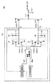
図1は、本発明の実施の形態に係る電源装置の構成を示す図である。
図1を参照して、電源装置201は、半導体集積回路101と、PチャネルMOSトランジスタM11と、NチャネルMOSトランジスタM12と、コイルL11と、コンデンサC11とを備える。半導体集積回路101は、スイッチング制御回路1Aおよび1Bと、バイアス回路2Aおよび2Bと、保護制御回路3と、異常検出回路11と、PWM(Pulse Width Modulation)制御回路12と、外部端子T1およびT2とを備える。スイッチング制御回路1Aは、PチャネルMOSトランジスタ(第1のトランジスタ)M1と、NチャネルMOSトランジスタ(第2のトランジスタ)M2とを含む。スイッチング制御回路1Bは、PチャネルMOSトランジスタ(第2のトランジスタ)M3と、NチャネルMOSトランジスタ(第1のトランジスタ)M4とを含む。バイアス回路2Aは、抵抗R1を含む。バイアス回路2Bは、抵抗R2を含む。
FIG. 1 is a diagram showing a configuration of a power supply device according to an embodiment of the present invention.
Referring to FIG. 1,
PチャネルMOSトランジスタM1は、ソース(第1の導通電極)が電源電位(第1の固定電位)に結合される。NチャネルMOSトランジスタM2は、ドレイン(第1の導通電極)がPチャネルMOSトランジスタM1のドレイン(第2の導通電極)に結合され、ソース(第2の導通電極)が接地電位(第2の固定電位)に結合される。抵抗R1は、第1端が電源電位に結合され、第2端がPチャネルMOSトランジスタM1のドレインおよびNチャネルMOSトランジスタM2のドレインに結合される。 P channel MOS transistor M1 has a source (first conductive electrode) coupled to a power supply potential (first fixed potential). N-channel MOS transistor M2 has a drain (first conduction electrode) coupled to a drain (second conduction electrode) of P-channel MOS transistor M1, and a source (second conduction electrode) ground potential (second fixed electrode). Potential). Resistor R1 has a first end coupled to the power supply potential and a second end coupled to the drain of P-channel MOS transistor M1 and the drain of N-channel MOS transistor M2.
PチャネルMOSトランジスタM11は、ゲート(制御電極)が外部端子T1を介してPチャネルMOSトランジスタM1のドレインおよびNチャネルMOSトランジスタM2のドレインに結合される。 P channel MOS transistor M11 has a gate (control electrode) coupled to the drain of P channel MOS transistor M1 and the drain of N channel MOS transistor M2 via external terminal T1.
PチャネルMOSトランジスタM11は、PチャネルMOSトランジスタM1がオン状態であり、かつNチャネルMOSトランジスタM2がオフ状態のときにゲート電位が電源電位となり、オフ状態となる。また、PチャネルMOSトランジスタM11は、PチャネルMOSトランジスタM1がオフ状態であり、かつNチャネルMOSトランジスタM2がオン状態のときにゲート電位が接地電位となり、オン状態となる。 P-channel MOS transistor M11 is turned off when the P-channel MOS transistor M1 is in the on state and the N-channel MOS transistor M2 is in the off state, so that the gate potential becomes the power supply potential. The P channel MOS transistor M11 is turned on when the P channel MOS transistor M1 is in the off state and the N channel MOS transistor M2 is in the on state, and the gate potential becomes the ground potential.
バイアス回路2Aは、PチャネルMOSトランジスタM1またはNチャネルMOSトランジスタM2がオン状態である場合には、PチャネルMOSトランジスタM11のゲート電位に影響を及ぼさない。バイアス回路2Aは、PチャネルMOSトランジスタM1およびNチャネルMOSトランジスタM2がオフ状態の場合に、PチャネルMOSトランジスタM11をオフ状態とするためのバイアス電圧すなわち電源電圧をPチャネルMOSトランジスタM11のゲートに供給する。
PチャネルMOSトランジスタM3は、ソース(第1の導通電極)が電源電位(第1の固定電位)に結合される。NチャネルMOSトランジスタM4は、ドレイン(第1の導通電極)がPチャネルMOSトランジスタM3のドレイン(第2の導通電極)に結合され、ソース(第2の導通電極)が接地電位(第2の固定電位)に結合される。抵抗R2は、第1端が接地電位に結合され、第2端がPチャネルMOSトランジスタM3のドレインおよびNチャネルMOSトランジスタM4のドレインに結合される。 P channel MOS transistor M3 has a source (first conduction electrode) coupled to a power supply potential (first fixed potential). N channel MOS transistor M4 has a drain (first conduction electrode) coupled to a drain (second conduction electrode) of P channel MOS transistor M3, and a source (second conduction electrode) ground potential (second fixed electrode). Potential). Resistor R2 has a first end coupled to the ground potential and a second end coupled to the drain of P-channel MOS transistor M3 and the drain of N-channel MOS transistor M4.
NチャネルMOSトランジスタM12は、ゲート(制御電極)が外部端子T2を介してPチャネルMOSトランジスタM3のドレインおよびNチャネルMOSトランジスタM4のドレインに結合される。 N channel MOS transistor M12 has a gate (control electrode) coupled to the drain of P channel MOS transistor M3 and the drain of N channel MOS transistor M4 via external terminal T2.
NチャネルMOSトランジスタM12は、PチャネルMOSトランジスタM3がオン状態であり、かつNチャネルMOSトランジスタM4がオフ状態のときにゲート電位が電源電位となり、オン状態となる。また、NチャネルMOSトランジスタM12は、PチャネルMOSトランジスタM3がオフ状態であり、かつNチャネルMOSトランジスタM4がオン状態のときにゲート電位が接地電位となり、オフ状態となる。 N-channel MOS transistor M12 is turned on when the P-channel MOS transistor M3 is in the on state and the N-channel MOS transistor M4 is in the off state, with the gate potential being the power supply potential. N-channel MOS transistor M12 is turned off when the P-channel MOS transistor M3 is in the off state and the N-channel MOS transistor M4 is in the on state, the gate potential being the ground potential.
バイアス回路2Bは、PチャネルMOSトランジスタM3またはNチャネルMOSトランジスタM4がオン状態である場合には、NチャネルMOSトランジスタM12のゲート電位に影響を及ぼさない。バイアス回路2Bは、PチャネルMOSトランジスタM3およびNチャネルMOSトランジスタM4がオフ状態の場合に、NチャネルMOSトランジスタM12をオフ状態とするためのバイアス電圧すなわち接地電圧をNチャネルMOSトランジスタM12のゲートに供給する。
PWM(Pulse Width Modulation)制御回路12は、PチャネルMOSトランジスタM11およびNチャネルMOSトランジスタM12のオン状態およびオフ状態を排他的に切り替えるためのPWM信号を保護制御回路3へ出力する。
The PWM (Pulse Width Modulation)
保護制御回路3は、PWM制御回路12から受けたPWM信号に基づいて制御信号CONT1〜CONT4を生成し、スイッチング制御回路1AにおけるPチャネルMOSトランジスタM1およびNチャネルMOSトランジスタM2、ならびにスイッチング制御回路1BにおけるPチャネルMOSトランジスタM3およびNチャネルMOSトランジスタM4へそれぞれ出力する。
The
スイッチング制御回路1Aおよび1Bは、保護制御回路3から受けた制御信号CONT1〜CONT4に基づいて、PチャネルMOSトランジスタM11およびNチャネルMOSトランジスタM12のオン状態およびオフ状態をそれぞれ切り替える。
Switching
PチャネルMOSトランジスタM11およびNチャネルMOSトランジスタM12のオン状態およびオフ状態の切り替えによって発生した交流電圧は、コイルL11およびコンデンサC11によって平滑化され、電源電圧として外部へ出力される。 The AC voltage generated by switching the on-state and off-state of P-channel MOS transistor M11 and N-channel MOS transistor M12 is smoothed by coil L11 and capacitor C11, and is output to the outside as a power supply voltage.
異常検出回路11は、半導体集積回路101の出力電圧すなわち外部端子T1およびT2における電圧をそれぞれ監視し、半導体集積回路101の出力電圧に異常が発生したと判断した場合には異常検出信号DETを保護制御回路3へ出力する。
The
保護制御回路3は、異常検出回路11から異常検出信号DETを受けると、PWM制御回路12から受けたPWM信号に関わらずPチャネルMOSトランジスタM1をオン状態とし、かつNチャネルMOSトランジスタM2をオフ状態とすることによりPチャネルMOSトランジスタM11をオフ状態とする。また、保護制御回路3は、異常検出回路11から異常検出信号DETを受けると、PWM制御回路12から受けたPWM信号に関わらずPチャネルMOSトランジスタM3をオフ状態とし、かつNチャネルMOSトランジスタM4をオン状態とすることによりNチャネルMOSトランジスタM12をオフ状態とする。
When receiving the abnormality detection signal DET from the
そして、保護制御回路3は、所定時間経過後、PチャネルMOSトランジスタM1およびM3ならびにNチャネルMOSトランジスタM2およびM4をオフ状態とする。
Then, after a predetermined time has elapsed,
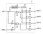
図2は、本発明の実施の形態に係る電源装置における半導体集積回路が備える保護制御回路の構成を示す図である。 FIG. 2 is a diagram showing a configuration of a protection control circuit included in the semiconductor integrated circuit in the power supply device according to the embodiment of the present invention.
図2を参照して、保護制御回路3は、NOT回路G1〜G3と、NOR回路G4と、NAND回路G5と、OR回路G6およびG7と、AND回路G8およびG9と、遅延回路21とを含む。
Referring to FIG. 2,
NOT回路G1と、NOR回路G4と、遅延回路21とは、異常検出回路11から異常検出信号DETを受ける。NOT回路G2は、PWM制御回路12からPWM信号を受ける。
The NOT circuit G1, the NOR circuit G4, and the
遅延回路21は、異常検出信号DETを所定時間遅延させ、遅延させた信号をNOT回路G3と、OR回路G6およびG7とへ出力する。遅延回路21は、たとえば、コンデンサおよび抵抗を含むアナログ回路で構成することができ、また、カウンタを含むデジタル回路で構成することもできる。
OR回路G6は、PチャネルMOSトランジスタM1のゲートへ制御信号CONT1を出力する。AND回路G8は、NチャネルMOSトランジスタM2のゲートへ制御信号CONT2を出力する。OR回路G7は、PチャネルMOSトランジスタM3のゲートへ制御信号CONT3を出力する。AND回路G9は、NチャネルMOSトランジスタM4のゲートへ制御信号CONT4を出力する。 OR circuit G6 outputs control signal CONT1 to the gate of P-channel MOS transistor M1. AND circuit G8 outputs control signal CONT2 to the gate of N-channel MOS transistor M2. OR circuit G7 outputs control signal CONT3 to the gate of P-channel MOS transistor M3. AND circuit G9 outputs control signal CONT4 to the gate of N-channel MOS transistor M4.
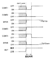
図3は、保護制御回路3の動作を示すタイミングチャートである。ここでは、異常検出信号DETがLレベルの場合には異常検出回路11において異常が検出されていない状態であり、異常検出信号DETがHレベルの場合には異常検出回路11において異常が検出された状態であると仮定する。
FIG. 3 is a timing chart showing the operation of the
図3を参照して、保護制御回路3は、異常検出信号DETがLレベルの場合には、PWM信号に基づいて制御信号CONT1〜CONT4の論理レベルを決定する。
Referring to FIG. 3,
異常検出信号DETがLレベルからHレベルに変化した時から所定の遅延時間が経過するまでの期間において、保護制御回路3は、制御信号CONT1をLレベルとし、制御信号CONT2をLレベルとし、制御信号CONT3をHレベルとし、制御信号CONT4をHレベルとする。すなわち、保護制御回路3は、PチャネルMOSトランジスタM1をオン状態とし、かつNチャネルMOSトランジスタM2をオフ状態とすることによりドライブ信号DRVAをHレベルとしてPチャネルMOSトランジスタM11をオフ状態とする。また、保護制御回路3は、PチャネルMOSトランジスタM3をオフ状態とし、かつNチャネルMOSトランジスタM4をオン状態とすることによりドライブ信号DRVBをLレベルとしてNチャネルMOSトランジスタM12をオフ状態とする。
In a period from when the abnormality detection signal DET changes from L level to H level until a predetermined delay time elapses, the
そして、保護制御回路3は、所定の遅延時間経過後、制御信号CONT1をHレベルとし、制御信号CONT2をLレベルとし、制御信号CONT3をHレベルとし、制御信号CONT4をLレベルとする。すなわち、保護制御回路3は、PチャネルMOSトランジスタM1およびM3ならびにNチャネルMOSトランジスタM2およびM4をオフ状態とする。このとき、バイアス回路2Aは、電源電位にプルアップされている抵抗R1により、ドライブ信号DRVAをHレベルに維持する、すなわちPチャネルMOSトランジスタM11のオフ状態を維持する。また、バイアス回路2Bは、接地電位にプルダウンされている抵抗R2により、ドライブ信号DRVBをLレベルに維持する、すなわちNチャネルMOSトランジスタM12のオフ状態を維持する。
Then, after a predetermined delay time has elapsed, the
なお、保護制御回路3は、異常検出回路11において異常が検出された場合に限らず、正常時に電源装置201を停止させる場合においても図3に示すような制御を行なうことにより、半導体集積回路101の構成の簡易化を図ることができる。
Note that the
ところで、従来のFET駆動ICでは、外部FETのオン状態およびオフ状態を切り替えるスイッチング制御回路の出力が接続される外部端子が接地電位または電源電位等とショートした場合には、外部FETをオフ状態とすることができても、スイッチング制御回路におけるオン状態のMOSトランジスタに大電流が流れて破壊されてしまう場合がある。あるいは、外部FETの寄生容量、および通常数10kΩを有するプルアップ抵抗またはプルダウン抵抗に起因して、外部FETのゲートの電位をオン状態に対応する電位からオフ状態に対応する電位に遷移させるまでに要する時間が長くなってしまい、外部FETまたは外部FETの次段の回路が破壊される場合がある。 By the way, in the conventional FET drive IC, when the external terminal to which the output of the switching control circuit for switching the ON state and the OFF state of the external FET is connected is short-circuited to the ground potential or the power supply potential, the external FET is turned off. Even if it can be done, a large current may flow through the on-state MOS transistor in the switching control circuit and be destroyed. Alternatively, due to the parasitic capacitance of the external FET and the pull-up resistor or pull-down resistor normally having several tens of kΩ, the potential of the gate of the external FET is changed from the potential corresponding to the ON state to the potential corresponding to the OFF state. The time required may become long, and the external FET or the next stage circuit of the external FET may be destroyed.
しかしながら、本発明の実施の形態に係る半導体集積回路は、保護制御回路3は、異常が検出された場合には、スイッチング制御回路における一方のMOSトランジスタをオン状態とし、かつ他方のMOSトランジスタがオフ状態とすることにより外部FETをオフ状態とし、所定時間経過後、2個のMOSトランジスタをオフ状態とする。そして、バイアス回路が、外部FETをオフ状態とするためのバイアス電圧を外部FETに供給する。
However, in the semiconductor integrated circuit according to the embodiment of the present invention, when an abnormality is detected, the
したがって、本発明の実施の形態に係る半導体集積回路は、異常発生時に外部FETを迅速にオフ状態として外部FETおよび外部FETの次段の回路を確実に保護することができ、かつ外部FETを駆動するための半導体集積回路におけるトランジスタ等の回路を保護することができる。 Therefore, in the semiconductor integrated circuit according to the embodiment of the present invention, when an abnormality occurs, the external FET can be quickly turned off to reliably protect the external FET and the circuit following the external FET, and drive the external FET. Therefore, a circuit such as a transistor in the semiconductor integrated circuit can be protected.
なお、本発明の実施の形態に係る電源装置は、半導体集積回路101の外部FETとしてPチャネルMOSトランジスタM11およびNチャネルMOSトランジスタM12を備える構成であるとしたが、これに限定するものではない。MOSトランジスタに限らず、他の種類のFETであってもよい。また、電源装置201は、半導体集積回路101の外部FETとして2個のPチャネルMOSトランジスタを備える構成であってもよいし、2個のNチャネルMOSトランジスタを備える構成であってもよい。
Although the power supply device according to the embodiment of the present invention is configured to include the P-channel MOS transistor M11 and the N-channel MOS transistor M12 as the external FET of the semiconductor integrated
今回開示された実施の形態はすべての点で例示であって制限的なものではないと考えられるべきである。本発明の範囲は上記した説明ではなくて特許請求の範囲によって示され、特許請求の範囲と均等の意味および範囲内でのすべての変更が含まれることが意図される。 The embodiment disclosed this time should be considered as illustrative in all points and not restrictive. The scope of the present invention is defined by the terms of the claims, rather than the description above, and is intended to include any modifications within the scope and meaning equivalent to the terms of the claims.
1A,1B スイッチング制御回路、2A,2B バイアス回路、3 保護制御回路、11 異常検出回路、12 PWM制御回路、21 遅延回路、101 半導体集積回路、201 電源装置、M11 PチャネルMOSトランジスタ、M12 NチャネルMOSトランジスタ、L11 コイル、C11 コンデンサ、T1,T2 外部端子、M1 PチャネルMOSトランジスタ(第1のトランジスタ)、M2 NチャネルMOSトランジスタ(第2のトランジスタ)、M3 PチャネルMOSトランジスタ(第2のトランジスタ)、M4 NチャネルMOSトランジスタ(第1のトランジスタ)、R1,R2 抵抗、G1〜G3 NOT回路、G4 NOR回路、G5 NAND回路、G6,G7 OR回路、G8,G9 AND回路。 1A, 1B switching control circuit, 2A, 2B bias circuit, 3 protection control circuit, 11 abnormality detection circuit, 12 PWM control circuit, 21 delay circuit, 101 semiconductor integrated circuit, 201 power supply device, M11 P channel MOS transistor, M12 N channel MOS transistor, L11 coil, C11 capacitor, T1, T2 external terminals, M1 P-channel MOS transistor (first transistor), M2 N-channel MOS transistor (second transistor), M3 P-channel MOS transistor (second transistor) , M4 N-channel MOS transistor (first transistor), R1, R2 resistance, G1-G3 NOT circuit, G4 NOR circuit, G5 NAND circuit, G6, G7 OR circuit, G8, G9 AND circuit.
Claims (3)
前記FETに結合される第1のトランジスタおよび第2のトランジスタを含み、前記第1のトランジスタおよび第2のトランジスタの各々をオン・オフすることにより前記FETをオン・オフするスイッチング制御回路を備え、
前記FETは、前記第1のトランジスタがオン状態であり、かつ前記第2のトランジスタがオフ状態のときにオフ状態となり、
前記半導体集積回路は、さらに、
前記第1のトランジスタおよび前記第2のトランジスタがオフ状態の場合、前記FETをオフするためのバイアス電圧を前記FETに供給するバイアス回路と、
異常が検出された場合には、前記第1のトランジスタをオンし、かつ前記第2のトランジスタをオフすることにより前記FETをオフし、所定時間経過後、前記第1のトランジスタおよび前記第2のトランジスタをオフする保護制御回路とを備える半導体集積回路。 A semiconductor integrated circuit for driving an external FET,
It comprises a first transistor and a second transistor coupled to said FET, a switching control circuit on Ofusu Ru said FET by turning on and off each of the first transistor and the second transistor ,
The FET is off when the first transistor is on and the second transistor is off,
The semiconductor integrated circuit further includes:
A bias circuit for supplying a bias voltage to the FET to turn off the FET when the first transistor and the second transistor are in an off state;
When an abnormality is detected, the FET is turned off by turning on the first transistor and turning off the second transistor. After a predetermined time has elapsed, the first transistor and the second transistor are turned off . A semiconductor integrated circuit comprising a protection control circuit for turning off a transistor.
前記第2のトランジスタは、第1の導通電極が前記FETの制御電極に結合され、第2の導通電極が第2の固定電位に結合され、
前記バイアス回路は、第1端が前記第1の固定電位に結合され、第2端が前記FETの制御電極に結合される抵抗を含み、
前記FETは、前記制御電極の電位が前記第1の固定電位となったときにオフする請求項1記載の半導体集積回路。 The first transistor has a first conduction electrode coupled to a first fixed potential, a second conduction electrode coupled to a control electrode of the FET,
The second transistor has a first conduction electrode coupled to the control electrode of the FET, a second conduction electrode coupled to a second fixed potential,
The bias circuit includes a resistor having a first end coupled to the first fixed potential and a second end coupled to a control electrode of the FET;
The semiconductor integrated circuit according to claim 1, wherein the FET is turned off when the potential of the control electrode becomes the first fixed potential.
半導体集積回路とを備え、
前記半導体集積回路は、
前記FETに結合される第1のトランジスタおよび第2のトランジスタを有し、前記第1のトランジスタおよび第2のトランジスタの各々をオン・オフすることにより前記FETをオン・オフするスイッチング制御回路を含み、
前記FETは、前記第1のトランジスタがオン状態であり、かつ前記第2のトランジスタがオフ状態のときにオフ状態となり、
前記半導体集積回路は、さらに、
前記第1のトランジスタおよび前記第2のトランジスタがオフ状態の場合、前記FETをオフするためのバイアス電圧を前記FETに供給するバイアス回路と、
異常が検出された場合には、前記第1のトランジスタをオンし、かつ前記第2のトランジスタをオフすることにより前記FETをオフし、所定時間経過後、前記第1のトランジスタおよび前記第2のトランジスタをオフする保護制御回路とを含む電源装置。 FET,
A semiconductor integrated circuit,
The semiconductor integrated circuit is:
Having a first transistor and a second transistor coupled to the FET, the switching control circuit on Ofusu Ru said FET by turning on and off each of the first transistor and the second transistor Including
The FET is off when the first transistor is on and the second transistor is off,
The semiconductor integrated circuit further includes:
A bias circuit for supplying a bias voltage to the FET to turn off the FET when the first transistor and the second transistor are in an off state;
When an abnormality is detected, the FET is turned off by turning on the first transistor and turning off the second transistor. After a predetermined time has elapsed, the first transistor and the second transistor are turned off . power supply comprising a protection control circuit for turning off the transistor.
Priority Applications (3)
| Application Number | Priority Date | Filing Date | Title |
|---|---|---|---|
| JP2006329378A JP4880436B2 (en) | 2006-12-06 | 2006-12-06 | Semiconductor integrated circuit and power supply device |
| CNA2007101971239A CN101197537A (en) | 2006-12-06 | 2007-12-05 | Semiconductor integrated circuit driving external fet and power supply incorporating the same |
| US11/951,692 US7724047B2 (en) | 2006-12-06 | 2007-12-06 | Semiconductor integrated circuit driving external FET and power supply incorporating the same |
Applications Claiming Priority (1)
| Application Number | Priority Date | Filing Date | Title |
|---|---|---|---|
| JP2006329378A JP4880436B2 (en) | 2006-12-06 | 2006-12-06 | Semiconductor integrated circuit and power supply device |
Publications (3)
| Publication Number | Publication Date |
|---|---|
| JP2008148378A JP2008148378A (en) | 2008-06-26 |
| JP2008148378A5 JP2008148378A5 (en) | 2010-02-12 |
| JP4880436B2 true JP4880436B2 (en) | 2012-02-22 |
Family
ID=39497228
Family Applications (1)
| Application Number | Title | Priority Date | Filing Date |
|---|---|---|---|
| JP2006329378A Expired - Fee Related JP4880436B2 (en) | 2006-12-06 | 2006-12-06 | Semiconductor integrated circuit and power supply device |
Country Status (3)
| Country | Link |
|---|---|
| US (1) | US7724047B2 (en) |
| JP (1) | JP4880436B2 (en) |
| CN (1) | CN101197537A (en) |
Families Citing this family (5)
| Publication number | Priority date | Publication date | Assignee | Title |
|---|---|---|---|---|
| JP2012065235A (en) * | 2010-09-17 | 2012-03-29 | Toshiba Corp | Voltage output circuit |
| JP5849735B2 (en) * | 2012-01-31 | 2016-02-03 | 株式会社デンソー | Driving device for driven switching element |
| CN103207339B (en) * | 2013-04-28 | 2015-09-30 | 科博达技术有限公司 | Inverter over-current judging method and device thereof |
| JP6225541B2 (en) * | 2013-07-29 | 2017-11-08 | 富士通株式会社 | Semiconductor device |
| CN106067821B (en) * | 2016-07-20 | 2023-04-14 | 成都博思微科技有限公司 | Protection circuit of high-speed buffer and implementation method thereof |
Family Cites Families (7)
| Publication number | Priority date | Publication date | Assignee | Title |
|---|---|---|---|---|
| KR960009247B1 (en) * | 1993-06-08 | 1996-07-16 | Samsung Electronics Co Ltd | Data output buffer of semiconductor integrated circuit |
| JPH07263627A (en) * | 1994-03-18 | 1995-10-13 | Nissan Motor Co Ltd | Load control device |
| JP2000201475A (en) | 1999-01-04 | 2000-07-18 | Texas Instr Japan Ltd | Power supply equipment |
| JP4066231B2 (en) | 2002-02-08 | 2008-03-26 | ローム株式会社 | Switching regulator |
| JP2004088245A (en) | 2002-08-23 | 2004-03-18 | Audio Technica Corp | Digital power amplifier for audio |
| GB0314563D0 (en) * | 2003-06-21 | 2003-07-30 | Koninkl Philips Electronics Nv | Dead time control in a switching circuit |
| JP4337711B2 (en) * | 2004-11-17 | 2009-09-30 | 株式会社デンソー | Semiconductor element control device |
-
2006
- 2006-12-06 JP JP2006329378A patent/JP4880436B2/en not_active Expired - Fee Related
-
2007
- 2007-12-05 CN CNA2007101971239A patent/CN101197537A/en active Pending
- 2007-12-06 US US11/951,692 patent/US7724047B2/en not_active Expired - Fee Related
Also Published As
| Publication number | Publication date |
|---|---|
| US20080136466A1 (en) | 2008-06-12 |
| US7724047B2 (en) | 2010-05-25 |
| JP2008148378A (en) | 2008-06-26 |
| CN101197537A (en) | 2008-06-11 |
Similar Documents
| Publication | Publication Date | Title |
|---|---|---|
| US7034573B1 (en) | Level shifter without DC current flow | |
| JP5537270B2 (en) | Output circuit | |
| US7486127B2 (en) | Transistor switch with integral body connection to prevent latchup | |
| JP2008147755A (en) | Driving circuit and semiconductor device using the same | |
| KR20150071339A (en) | Gate driver circuit | |
| US10355685B2 (en) | Output circuit | |
| JP4618164B2 (en) | Switch circuit | |
| US20090085639A1 (en) | Output buffer circuit | |
| JP4880436B2 (en) | Semiconductor integrated circuit and power supply device | |
| TWI415388B (en) | Level shift circuit without high voltage stress of trasistors and operating at low voltages | |
| JP5160320B2 (en) | Switching drive circuit | |
| JP2011120158A (en) | Semiconductor device, and power supply switch circuit | |
| JP2011103607A (en) | Input circuit | |
| JP2003133944A (en) | Interface system between ics and ic | |
| US20070120577A1 (en) | Semiconductor integrated apparatus using two or more types of power supplies | |
| US8395420B2 (en) | Input buffer circuit | |
| US20130120886A1 (en) | Driving circuits with power mos breakdown protection and driving methods thereof | |
| JP2007033113A (en) | Overcurrent detection circuit | |
| JP2004180241A (en) | Analog switch circuit | |
| US7327621B2 (en) | Current sense amplifier with lower sensing error rate by using smaller sensing current difference | |
| JP4175193B2 (en) | MOS type semiconductor integrated circuit | |
| JP2005085980A (en) | Fuse circuit | |
| JP4680423B2 (en) | Output circuit | |
| JP4207773B2 (en) | Inverter circuit | |
| JP2009188790A (en) | Output buffer circuit |
Legal Events
| Date | Code | Title | Description |
|---|---|---|---|
| A621 | Written request for application examination |
Free format text: JAPANESE INTERMEDIATE CODE: A621 Effective date: 20090825 |
|
| A521 | Request for written amendment filed |
Free format text: JAPANESE INTERMEDIATE CODE: A523 Effective date: 20091221 |
|
| A977 | Report on retrieval |
Free format text: JAPANESE INTERMEDIATE CODE: A971007 Effective date: 20111117 |
|
| TRDD | Decision of grant or rejection written | ||
| A01 | Written decision to grant a patent or to grant a registration (utility model) |
Free format text: JAPANESE INTERMEDIATE CODE: A01 Effective date: 20111122 |
|
| A01 | Written decision to grant a patent or to grant a registration (utility model) |
Free format text: JAPANESE INTERMEDIATE CODE: A01 |
|
| A61 | First payment of annual fees (during grant procedure) |
Free format text: JAPANESE INTERMEDIATE CODE: A61 Effective date: 20111201 |
|
| R150 | Certificate of patent or registration of utility model |
Free format text: JAPANESE INTERMEDIATE CODE: R150 |
|
| FPAY | Renewal fee payment (event date is renewal date of database) |
Free format text: PAYMENT UNTIL: 20141209 Year of fee payment: 3 |
|
| LAPS | Cancellation because of no payment of annual fees |