JP4877675B2 - Method for manufacturing electro-optical device - Google Patents
Method for manufacturing electro-optical device Download PDFInfo
- Publication number
- JP4877675B2 JP4877675B2 JP2000194845A JP2000194845A JP4877675B2 JP 4877675 B2 JP4877675 B2 JP 4877675B2 JP 2000194845 A JP2000194845 A JP 2000194845A JP 2000194845 A JP2000194845 A JP 2000194845A JP 4877675 B2 JP4877675 B2 JP 4877675B2
- Authority
- JP
- Japan
- Prior art keywords
- film
- layer
- tft
- gate
- roll
- Prior art date
- Legal status (The legal status is an assumption and is not a legal conclusion. Google has not performed a legal analysis and makes no representation as to the accuracy of the status listed.)
- Expired - Fee Related
Links
- 238000000034 method Methods 0.000 title claims description 62
- 238000004519 manufacturing process Methods 0.000 title claims description 26
- 239000000463 material Substances 0.000 claims description 92
- 239000000758 substrate Substances 0.000 claims description 44
- 238000007639 printing Methods 0.000 claims description 31
- 230000015572 biosynthetic process Effects 0.000 claims description 26
- 230000017525 heat dissipation Effects 0.000 claims description 22
- 239000004065 semiconductor Substances 0.000 claims description 21
- 230000006870 function Effects 0.000 claims description 15
- 229920005989 resin Polymers 0.000 claims description 13
- 239000011347 resin Substances 0.000 claims description 13
- TWNQGVIAIRXVLR-UHFFFAOYSA-N oxo(oxoalumanyloxy)alumane Chemical compound O=[Al]O[Al]=O TWNQGVIAIRXVLR-UHFFFAOYSA-N 0.000 claims description 5
- 239000012808 vapor phase Substances 0.000 claims description 3
- 230000005540 biological transmission Effects 0.000 claims 2
- 239000010408 film Substances 0.000 description 248
- 239000010410 layer Substances 0.000 description 128
- 238000002161 passivation Methods 0.000 description 49
- 239000012535 impurity Substances 0.000 description 29
- 230000000694 effects Effects 0.000 description 25
- 239000011229 interlayer Substances 0.000 description 24
- 230000001681 protective effect Effects 0.000 description 24
- 229910052581 Si3N4 Inorganic materials 0.000 description 17
- 229910052783 alkali metal Inorganic materials 0.000 description 17
- 150000001340 alkali metals Chemical class 0.000 description 17
- 239000012298 atmosphere Substances 0.000 description 17
- 239000011159 matrix material Substances 0.000 description 17
- 229910052710 silicon Inorganic materials 0.000 description 17
- HQVNEWCFYHHQES-UHFFFAOYSA-N silicon nitride Chemical compound N12[Si]34N5[Si]62N3[Si]51N64 HQVNEWCFYHHQES-UHFFFAOYSA-N 0.000 description 17
- XUIMIQQOPSSXEZ-UHFFFAOYSA-N Silicon Chemical compound [Si] XUIMIQQOPSSXEZ-UHFFFAOYSA-N 0.000 description 14
- 238000002347 injection Methods 0.000 description 14
- 239000007924 injection Substances 0.000 description 14
- 229910052760 oxygen Inorganic materials 0.000 description 14
- 239000010703 silicon Substances 0.000 description 14
- 239000002904 solvent Substances 0.000 description 14
- QVGXLLKOCUKJST-UHFFFAOYSA-N atomic oxygen Chemical compound [O] QVGXLLKOCUKJST-UHFFFAOYSA-N 0.000 description 13
- 239000002585 base Substances 0.000 description 13
- 239000001301 oxygen Substances 0.000 description 13
- IJGRMHOSHXDMSA-UHFFFAOYSA-N Atomic nitrogen Chemical compound N#N IJGRMHOSHXDMSA-UHFFFAOYSA-N 0.000 description 12
- 238000010438 heat treatment Methods 0.000 description 12
- 229910021419 crystalline silicon Inorganic materials 0.000 description 11
- 238000002425 crystallisation Methods 0.000 description 11
- 230000006866 deterioration Effects 0.000 description 11
- OAICVXFJPJFONN-UHFFFAOYSA-N Phosphorus Chemical compound [P] OAICVXFJPJFONN-UHFFFAOYSA-N 0.000 description 10
- 229910021417 amorphous silicon Inorganic materials 0.000 description 10
- -1 polyparaphenylene vinylene Polymers 0.000 description 10
- 229910052782 aluminium Inorganic materials 0.000 description 9
- 229910052757 nitrogen Inorganic materials 0.000 description 9
- 229910052698 phosphorus Inorganic materials 0.000 description 9
- 239000011574 phosphorus Substances 0.000 description 9
- 238000001994 activation Methods 0.000 description 8
- 239000011521 glass Substances 0.000 description 8
- 239000010409 thin film Substances 0.000 description 8
- 230000004913 activation Effects 0.000 description 7
- 239000000853 adhesive Substances 0.000 description 7
- 230000001070 adhesive effect Effects 0.000 description 7
- 230000008901 benefit Effects 0.000 description 7
- 239000003990 capacitor Substances 0.000 description 7
- 230000008025 crystallization Effects 0.000 description 7
- 239000011261 inert gas Substances 0.000 description 7
- 238000005070 sampling Methods 0.000 description 7
- VYPSYNLAJGMNEJ-UHFFFAOYSA-N silicon dioxide Inorganic materials O=[Si]=O VYPSYNLAJGMNEJ-UHFFFAOYSA-N 0.000 description 7
- 238000007740 vapor deposition Methods 0.000 description 7
- OKTJSMMVPCPJKN-UHFFFAOYSA-N Carbon Chemical compound [C] OKTJSMMVPCPJKN-UHFFFAOYSA-N 0.000 description 6
- UFHFLCQGNIYNRP-UHFFFAOYSA-N Hydrogen Chemical compound [H][H] UFHFLCQGNIYNRP-UHFFFAOYSA-N 0.000 description 6
- XAGFODPZIPBFFR-UHFFFAOYSA-N aluminium Chemical compound [Al] XAGFODPZIPBFFR-UHFFFAOYSA-N 0.000 description 6
- 229910052799 carbon Inorganic materials 0.000 description 6
- 239000001257 hydrogen Substances 0.000 description 6
- 229910052739 hydrogen Inorganic materials 0.000 description 6
- 150000002500 ions Chemical class 0.000 description 6
- 239000002356 single layer Substances 0.000 description 6
- 238000003860 storage Methods 0.000 description 6
- 239000010936 titanium Substances 0.000 description 6
- ZOXJGFHDIHLPTG-UHFFFAOYSA-N Boron Chemical compound [B] ZOXJGFHDIHLPTG-UHFFFAOYSA-N 0.000 description 5
- RTAQQCXQSZGOHL-UHFFFAOYSA-N Titanium Chemical compound [Ti] RTAQQCXQSZGOHL-UHFFFAOYSA-N 0.000 description 5
- 238000007774 anilox coating Methods 0.000 description 5
- 229910052796 boron Inorganic materials 0.000 description 5
- 239000000872 buffer Substances 0.000 description 5
- 239000007789 gas Substances 0.000 description 5
- 230000005525 hole transport Effects 0.000 description 5
- 238000005984 hydrogenation reaction Methods 0.000 description 5
- 239000011368 organic material Substances 0.000 description 5
- 230000010355 oscillation Effects 0.000 description 5
- 239000002861 polymer material Substances 0.000 description 5
- 238000004544 sputter deposition Methods 0.000 description 5
- 229910052719 titanium Inorganic materials 0.000 description 5
- 238000002834 transmittance Methods 0.000 description 5
- XKRFYHLGVUSROY-UHFFFAOYSA-N Argon Chemical compound [Ar] XKRFYHLGVUSROY-UHFFFAOYSA-N 0.000 description 4
- SECXISVLQFMRJM-UHFFFAOYSA-N N-Methylpyrrolidone Chemical compound CN1CCCC1=O SECXISVLQFMRJM-UHFFFAOYSA-N 0.000 description 4
- XYFCBTPGUUZFHI-UHFFFAOYSA-N Phosphine Chemical compound P XYFCBTPGUUZFHI-UHFFFAOYSA-N 0.000 description 4
- NIXOWILDQLNWCW-UHFFFAOYSA-N acrylic acid group Chemical group C(C=C)(=O)O NIXOWILDQLNWCW-UHFFFAOYSA-N 0.000 description 4
- QVQLCTNNEUAWMS-UHFFFAOYSA-N barium oxide Chemical compound [Ba]=O QVQLCTNNEUAWMS-UHFFFAOYSA-N 0.000 description 4
- UMIVXZPTRXBADB-UHFFFAOYSA-N benzocyclobutene Chemical compound C1=CC=C2CCC2=C1 UMIVXZPTRXBADB-UHFFFAOYSA-N 0.000 description 4
- 239000000919 ceramic Substances 0.000 description 4
- PMHQVHHXPFUNSP-UHFFFAOYSA-M copper(1+);methylsulfanylmethane;bromide Chemical compound Br[Cu].CSC PMHQVHHXPFUNSP-UHFFFAOYSA-M 0.000 description 4
- 230000007423 decrease Effects 0.000 description 4
- 238000010586 diagram Methods 0.000 description 4
- 239000004973 liquid crystal related substance Substances 0.000 description 4
- 239000011777 magnesium Substances 0.000 description 4
- 239000000203 mixture Substances 0.000 description 4
- 229920003227 poly(N-vinyl carbazole) Polymers 0.000 description 4
- 229920000553 poly(phenylenevinylene) Polymers 0.000 description 4
- 229920000642 polymer Polymers 0.000 description 4
- 230000008569 process Effects 0.000 description 4
- 229910052814 silicon oxide Inorganic materials 0.000 description 4
- 238000001771 vacuum deposition Methods 0.000 description 4
- YMWUJEATGCHHMB-UHFFFAOYSA-N Dichloromethane Chemical compound ClCCl YMWUJEATGCHHMB-UHFFFAOYSA-N 0.000 description 3
- 238000000137 annealing Methods 0.000 description 3
- 239000000969 carrier Substances 0.000 description 3
- 239000003054 catalyst Substances 0.000 description 3
- 150000001875 compounds Chemical class 0.000 description 3
- 239000013078 crystal Substances 0.000 description 3
- 229910003460 diamond Inorganic materials 0.000 description 3
- 239000010432 diamond Substances 0.000 description 3
- 239000007788 liquid Substances 0.000 description 3
- 229910052751 metal Inorganic materials 0.000 description 3
- 239000002184 metal Substances 0.000 description 3
- 229910021420 polycrystalline silicon Inorganic materials 0.000 description 3
- 239000002243 precursor Substances 0.000 description 3
- 239000011241 protective layer Substances 0.000 description 3
- 239000010453 quartz Substances 0.000 description 3
- 230000009467 reduction Effects 0.000 description 3
- 238000007650 screen-printing Methods 0.000 description 3
- 238000009751 slip forming Methods 0.000 description 3
- 229910052721 tungsten Inorganic materials 0.000 description 3
- 239000010937 tungsten Substances 0.000 description 3
- 150000005072 1,3,4-oxadiazoles Chemical class 0.000 description 2
- 239000004925 Acrylic resin Substances 0.000 description 2
- 229910052582 BN Inorganic materials 0.000 description 2
- PZNSFCLAULLKQX-UHFFFAOYSA-N Boron nitride Chemical compound N#B PZNSFCLAULLKQX-UHFFFAOYSA-N 0.000 description 2
- HEDRZPFGACZZDS-UHFFFAOYSA-N Chloroform Chemical compound ClC(Cl)Cl HEDRZPFGACZZDS-UHFFFAOYSA-N 0.000 description 2
- PXHVJJICTQNCMI-UHFFFAOYSA-N Nickel Chemical compound [Ni] PXHVJJICTQNCMI-UHFFFAOYSA-N 0.000 description 2
- 239000004952 Polyamide Substances 0.000 description 2
- 239000004642 Polyimide Substances 0.000 description 2
- 229910020286 SiOxNy Inorganic materials 0.000 description 2
- 229910020776 SixNy Inorganic materials 0.000 description 2
- PPBRXRYQALVLMV-UHFFFAOYSA-N Styrene Chemical compound C=CC1=CC=CC=C1 PPBRXRYQALVLMV-UHFFFAOYSA-N 0.000 description 2
- XLOMVQKBTHCTTD-UHFFFAOYSA-N Zinc monoxide Chemical compound [Zn]=O XLOMVQKBTHCTTD-UHFFFAOYSA-N 0.000 description 2
- 230000002411 adverse Effects 0.000 description 2
- 229910045601 alloy Inorganic materials 0.000 description 2
- 239000000956 alloy Substances 0.000 description 2
- 229910003481 amorphous carbon Inorganic materials 0.000 description 2
- 229910052786 argon Inorganic materials 0.000 description 2
- FFBGYFUYJVKRNV-UHFFFAOYSA-N boranylidynephosphane Chemical compound P#B FFBGYFUYJVKRNV-UHFFFAOYSA-N 0.000 description 2
- 239000011575 calcium Substances 0.000 description 2
- 230000015556 catabolic process Effects 0.000 description 2
- 238000006243 chemical reaction Methods 0.000 description 2
- 239000011651 chromium Substances 0.000 description 2
- 238000000576 coating method Methods 0.000 description 2
- 239000010949 copper Substances 0.000 description 2
- VBVAVBCYMYWNOU-UHFFFAOYSA-N coumarin 6 Chemical compound C1=CC=C2SC(C3=CC4=CC=C(C=C4OC3=O)N(CC)CC)=NC2=C1 VBVAVBCYMYWNOU-UHFFFAOYSA-N 0.000 description 2
- 238000006731 degradation reaction Methods 0.000 description 2
- 238000000151 deposition Methods 0.000 description 2
- 239000002274 desiccant Substances 0.000 description 2
- 238000009792 diffusion process Methods 0.000 description 2
- 239000003822 epoxy resin Substances 0.000 description 2
- 230000005669 field effect Effects 0.000 description 2
- 230000009477 glass transition Effects 0.000 description 2
- 238000007733 ion plating Methods 0.000 description 2
- 229910052746 lanthanum Inorganic materials 0.000 description 2
- 238000005224 laser annealing Methods 0.000 description 2
- 229910052749 magnesium Inorganic materials 0.000 description 2
- 238000012423 maintenance Methods 0.000 description 2
- 239000007769 metal material Substances 0.000 description 2
- 239000012299 nitrogen atmosphere Substances 0.000 description 2
- 150000002894 organic compounds Chemical class 0.000 description 2
- 230000003071 parasitic effect Effects 0.000 description 2
- 229910000073 phosphorus hydride Inorganic materials 0.000 description 2
- 229920002647 polyamide Polymers 0.000 description 2
- 229920000647 polyepoxide Polymers 0.000 description 2
- 229920001721 polyimide Polymers 0.000 description 2
- 229920005591 polysilicon Polymers 0.000 description 2
- 238000012545 processing Methods 0.000 description 2
- 230000001737 promoting effect Effects 0.000 description 2
- 238000000746 purification Methods 0.000 description 2
- 238000000926 separation method Methods 0.000 description 2
- HBMJWWWQQXIZIP-UHFFFAOYSA-N silicon carbide Chemical compound [Si+]#[C-] HBMJWWWQQXIZIP-UHFFFAOYSA-N 0.000 description 2
- 229910010271 silicon carbide Inorganic materials 0.000 description 2
- 229910052709 silver Inorganic materials 0.000 description 2
- 238000004528 spin coating Methods 0.000 description 2
- WFKWXMTUELFFGS-UHFFFAOYSA-N tungsten Chemical compound [W] WFKWXMTUELFFGS-UHFFFAOYSA-N 0.000 description 2
- POAOYUHQDCAZBD-UHFFFAOYSA-N 2-butoxyethanol Chemical compound CCCCOCCO POAOYUHQDCAZBD-UHFFFAOYSA-N 0.000 description 1
- 229920000178 Acrylic resin Polymers 0.000 description 1
- 229910000838 Al alloy Inorganic materials 0.000 description 1
- 229910016909 AlxOy Inorganic materials 0.000 description 1
- OYPRJOBELJOOCE-UHFFFAOYSA-N Calcium Chemical compound [Ca] OYPRJOBELJOOCE-UHFFFAOYSA-N 0.000 description 1
- 229910052684 Cerium Inorganic materials 0.000 description 1
- VYZAMTAEIAYCRO-UHFFFAOYSA-N Chromium Chemical compound [Cr] VYZAMTAEIAYCRO-UHFFFAOYSA-N 0.000 description 1
- RYGMFSIKBFXOCR-UHFFFAOYSA-N Copper Chemical compound [Cu] RYGMFSIKBFXOCR-UHFFFAOYSA-N 0.000 description 1
- 229910052692 Dysprosium Inorganic materials 0.000 description 1
- 229910052691 Erbium Inorganic materials 0.000 description 1
- 229910052688 Gadolinium Inorganic materials 0.000 description 1
- DGAQECJNVWCQMB-PUAWFVPOSA-M Ilexoside XXIX Chemical compound C[C@@H]1CC[C@@]2(CC[C@@]3(C(=CC[C@H]4[C@]3(CC[C@@H]5[C@@]4(CC[C@@H](C5(C)C)OS(=O)(=O)[O-])C)C)[C@@H]2[C@]1(C)O)C)C(=O)O[C@H]6[C@@H]([C@H]([C@@H]([C@H](O6)CO)O)O)O.[Na+] DGAQECJNVWCQMB-PUAWFVPOSA-M 0.000 description 1
- 229910010199 LiAl Inorganic materials 0.000 description 1
- WHXSMMKQMYFTQS-UHFFFAOYSA-N Lithium Chemical compound [Li] WHXSMMKQMYFTQS-UHFFFAOYSA-N 0.000 description 1
- FYYHWMGAXLPEAU-UHFFFAOYSA-N Magnesium Chemical compound [Mg] FYYHWMGAXLPEAU-UHFFFAOYSA-N 0.000 description 1
- ZOKXTWBITQBERF-UHFFFAOYSA-N Molybdenum Chemical compound [Mo] ZOKXTWBITQBERF-UHFFFAOYSA-N 0.000 description 1
- VCUFZILGIRCDQQ-KRWDZBQOSA-N N-[[(5S)-2-oxo-3-(2-oxo-3H-1,3-benzoxazol-6-yl)-1,3-oxazolidin-5-yl]methyl]-2-[[3-(trifluoromethoxy)phenyl]methylamino]pyrimidine-5-carboxamide Chemical compound O=C1O[C@H](CN1C1=CC2=C(NC(O2)=O)C=C1)CNC(=O)C=1C=NC(=NC=1)NCC1=CC(=CC=C1)OC(F)(F)F VCUFZILGIRCDQQ-KRWDZBQOSA-N 0.000 description 1
- 229910052779 Neodymium Inorganic materials 0.000 description 1
- 229910052772 Samarium Inorganic materials 0.000 description 1
- BQCADISMDOOEFD-UHFFFAOYSA-N Silver Chemical compound [Ag] BQCADISMDOOEFD-UHFFFAOYSA-N 0.000 description 1
- 229910001362 Ta alloys Inorganic materials 0.000 description 1
- GWEVSGVZZGPLCZ-UHFFFAOYSA-N Titan oxide Chemical compound O=[Ti]=O GWEVSGVZZGPLCZ-UHFFFAOYSA-N 0.000 description 1
- NRTOMJZYCJJWKI-UHFFFAOYSA-N Titanium nitride Chemical compound [Ti]#N NRTOMJZYCJJWKI-UHFFFAOYSA-N 0.000 description 1
- 229910001080 W alloy Inorganic materials 0.000 description 1
- 229910052769 Ytterbium Inorganic materials 0.000 description 1
- LEVVHYCKPQWKOP-UHFFFAOYSA-N [Si].[Ge] Chemical compound [Si].[Ge] LEVVHYCKPQWKOP-UHFFFAOYSA-N 0.000 description 1
- 238000010521 absorption reaction Methods 0.000 description 1
- 238000009825 accumulation Methods 0.000 description 1
- 239000000654 additive Substances 0.000 description 1
- 230000000996 additive effect Effects 0.000 description 1
- 239000012300 argon atmosphere Substances 0.000 description 1
- 229910052785 arsenic Inorganic materials 0.000 description 1
- RQNWIZPPADIBDY-UHFFFAOYSA-N arsenic atom Chemical compound [As] RQNWIZPPADIBDY-UHFFFAOYSA-N 0.000 description 1
- IVHJCRXBQPGLOV-UHFFFAOYSA-N azanylidynetungsten Chemical compound [W]#N IVHJCRXBQPGLOV-UHFFFAOYSA-N 0.000 description 1
- 230000000903 blocking effect Effects 0.000 description 1
- 239000005388 borosilicate glass Substances 0.000 description 1
- 229910052791 calcium Inorganic materials 0.000 description 1
- 238000005266 casting Methods 0.000 description 1
- ZMIGMASIKSOYAM-UHFFFAOYSA-N cerium Chemical compound [Ce][Ce][Ce][Ce][Ce][Ce][Ce][Ce][Ce][Ce][Ce][Ce][Ce][Ce][Ce][Ce][Ce][Ce][Ce][Ce][Ce][Ce][Ce][Ce][Ce][Ce][Ce][Ce][Ce][Ce][Ce][Ce][Ce][Ce][Ce][Ce][Ce][Ce] ZMIGMASIKSOYAM-UHFFFAOYSA-N 0.000 description 1
- 229910052804 chromium Inorganic materials 0.000 description 1
- 229910052802 copper Inorganic materials 0.000 description 1
- 238000012937 correction Methods 0.000 description 1
- 230000007547 defect Effects 0.000 description 1
- 238000013461 design Methods 0.000 description 1
- 230000002542 deteriorative effect Effects 0.000 description 1
- 238000011161 development Methods 0.000 description 1
- 238000007598 dipping method Methods 0.000 description 1
- KBQHZAAAGSGFKK-UHFFFAOYSA-N dysprosium atom Chemical compound [Dy] KBQHZAAAGSGFKK-UHFFFAOYSA-N 0.000 description 1
- 238000005401 electroluminescence Methods 0.000 description 1
- UYAHIZSMUZPPFV-UHFFFAOYSA-N erbium Chemical compound [Er] UYAHIZSMUZPPFV-UHFFFAOYSA-N 0.000 description 1
- 238000005530 etching Methods 0.000 description 1
- 125000005678 ethenylene group Chemical group [H]C([*:1])=C([H])[*:2] 0.000 description 1
- 238000001704 evaporation Methods 0.000 description 1
- UIWYJDYFSGRHKR-UHFFFAOYSA-N gadolinium atom Chemical compound [Gd] UIWYJDYFSGRHKR-UHFFFAOYSA-N 0.000 description 1
- 239000002241 glass-ceramic Substances 0.000 description 1
- RBTKNAXYKSUFRK-UHFFFAOYSA-N heliogen blue Chemical compound [Cu].[N-]1C2=C(C=CC=C3)C3=C1N=C([N-]1)C3=CC=CC=C3C1=NC([N-]1)=C(C=CC=C3)C3=C1N=C([N-]1)C3=CC=CC=C3C1=N2 RBTKNAXYKSUFRK-UHFFFAOYSA-N 0.000 description 1
- 229910052734 helium Inorganic materials 0.000 description 1
- 239000001307 helium Substances 0.000 description 1
- SWQJXJOGLNCZEY-UHFFFAOYSA-N helium atom Chemical compound [He] SWQJXJOGLNCZEY-UHFFFAOYSA-N 0.000 description 1
- 230000001771 impaired effect Effects 0.000 description 1
- APFVFJFRJDLVQX-UHFFFAOYSA-N indium atom Chemical compound [In] APFVFJFRJDLVQX-UHFFFAOYSA-N 0.000 description 1
- 229910003437 indium oxide Inorganic materials 0.000 description 1
- AMGQUBHHOARCQH-UHFFFAOYSA-N indium;oxotin Chemical compound [In].[Sn]=O AMGQUBHHOARCQH-UHFFFAOYSA-N 0.000 description 1
- 239000011810 insulating material Substances 0.000 description 1
- 238000009413 insulation Methods 0.000 description 1
- 238000005468 ion implantation Methods 0.000 description 1
- 239000005001 laminate film Substances 0.000 description 1
- 238000010030 laminating Methods 0.000 description 1
- FZLIPJUXYLNCLC-UHFFFAOYSA-N lanthanum atom Chemical compound [La] FZLIPJUXYLNCLC-UHFFFAOYSA-N 0.000 description 1
- 238000005499 laser crystallization Methods 0.000 description 1
- 238000007644 letterpress printing Methods 0.000 description 1
- 229910052744 lithium Inorganic materials 0.000 description 1
- QLOAVXSYZAJECW-UHFFFAOYSA-N methane;molecular fluorine Chemical compound C.FF QLOAVXSYZAJECW-UHFFFAOYSA-N 0.000 description 1
- 238000002156 mixing Methods 0.000 description 1
- 229910052750 molybdenum Inorganic materials 0.000 description 1
- 239000011733 molybdenum Substances 0.000 description 1
- QEFYFXOXNSNQGX-UHFFFAOYSA-N neodymium atom Chemical compound [Nd] QEFYFXOXNSNQGX-UHFFFAOYSA-N 0.000 description 1
- 229910052759 nickel Inorganic materials 0.000 description 1
- 150000004767 nitrides Chemical class 0.000 description 1
- 238000010943 off-gassing Methods 0.000 description 1
- 230000003287 optical effect Effects 0.000 description 1
- 239000003960 organic solvent Substances 0.000 description 1
- 238000004806 packaging method and process Methods 0.000 description 1
- 230000035515 penetration Effects 0.000 description 1
- 238000005268 plasma chemical vapour deposition Methods 0.000 description 1
- 238000009832 plasma treatment Methods 0.000 description 1
- 239000004033 plastic Substances 0.000 description 1
- 229920003023 plastic Polymers 0.000 description 1
- 239000002985 plastic film Substances 0.000 description 1
- 229920006255 plastic film Polymers 0.000 description 1
- 229920005668 polycarbonate resin Polymers 0.000 description 1
- 239000004431 polycarbonate resin Substances 0.000 description 1
- 229920002098 polyfluorene Polymers 0.000 description 1
- 229910052761 rare earth metal Inorganic materials 0.000 description 1
- 238000002310 reflectometry Methods 0.000 description 1
- 230000004044 response Effects 0.000 description 1
- KZUNJOHGWZRPMI-UHFFFAOYSA-N samarium atom Chemical compound [Sm] KZUNJOHGWZRPMI-UHFFFAOYSA-N 0.000 description 1
- 238000007789 sealing Methods 0.000 description 1
- 229910021332 silicide Inorganic materials 0.000 description 1
- FVBUAEGBCNSCDD-UHFFFAOYSA-N silicide(4-) Chemical compound [Si-4] FVBUAEGBCNSCDD-UHFFFAOYSA-N 0.000 description 1
- 229920002050 silicone resin Polymers 0.000 description 1
- 239000004332 silver Substances 0.000 description 1
- 229910052708 sodium Inorganic materials 0.000 description 1
- 239000011734 sodium Substances 0.000 description 1
- 239000000243 solution Substances 0.000 description 1
- 239000000126 substance Substances 0.000 description 1
- 229910052715 tantalum Inorganic materials 0.000 description 1
- GUVRBAGPIYLISA-UHFFFAOYSA-N tantalum atom Chemical compound [Ta] GUVRBAGPIYLISA-UHFFFAOYSA-N 0.000 description 1
- MZLGASXMSKOWSE-UHFFFAOYSA-N tantalum nitride Chemical compound [Ta]#N MZLGASXMSKOWSE-UHFFFAOYSA-N 0.000 description 1
- 229920001187 thermosetting polymer Polymers 0.000 description 1
- OGIDPMRJRNCKJF-UHFFFAOYSA-N titanium oxide Inorganic materials [Ti]=O OGIDPMRJRNCKJF-UHFFFAOYSA-N 0.000 description 1
- 229910021341 titanium silicide Inorganic materials 0.000 description 1
- WQJQOUPTWCFRMM-UHFFFAOYSA-N tungsten disilicide Chemical compound [Si]#[W]#[Si] WQJQOUPTWCFRMM-UHFFFAOYSA-N 0.000 description 1
- 229910021342 tungsten silicide Inorganic materials 0.000 description 1
- XLYOFNOQVPJJNP-UHFFFAOYSA-N water Substances O XLYOFNOQVPJJNP-UHFFFAOYSA-N 0.000 description 1
- NAWDYIZEMPQZHO-UHFFFAOYSA-N ytterbium Chemical compound [Yb] NAWDYIZEMPQZHO-UHFFFAOYSA-N 0.000 description 1
- 229910052727 yttrium Inorganic materials 0.000 description 1
- VWQVUPCCIRVNHF-UHFFFAOYSA-N yttrium atom Chemical compound [Y] VWQVUPCCIRVNHF-UHFFFAOYSA-N 0.000 description 1
- 239000011787 zinc oxide Substances 0.000 description 1
Images


Description
【0001】
【発明の属する技術分野】
本発明は半導体素子(半導体薄膜を用いた素子、代表的には薄膜トランジスタ)を基板上に作り込んで形成されたEL(エレクトロルミネッセンス)表示装置に代表される電気光学装置及びその電気光学装置を表示ディスプレイとして有する電子装置(電子機器)に関する。特にそれらの作製方法に関する。
【0002】
【従来の技術】
近年、基板上に薄膜トランジスタ(以下、TFTという)を形成する技術が大幅に進歩し、アクティブマトリクス型表示装置への応用開発が進められている。特に、ポリシリコン膜を用いたTFTは、従来のアモルファスシリコン膜を用いたTFTよりも電界効果移動度が高いので、高速動作が可能である。そのため、従来、基板外の駆動回路で行っていた画素の制御を、画素と同一の基板上に形成した駆動回路で行うことが可能となっている。
【0003】
このようなアクティブマトリクス型表示装置は、同一基板上に様々な回路や素子を作り込むことで製造コストの低減、表示装置の小型化、歩留まりの上昇、スループットの低減など、様々な利点が得られるとして注目されている。
【0004】
アクティブマトリクス型EL表示装置は、各画素のそれぞれにTFTでなるスイッチング素子を設け、そのスイッチング素子によって電流制御を行う駆動素子を動作させてEL層(発光層)を発光させる。例えば米国特許番号5,684,365号(日本国公開公報:特開平8−234683号参照)、日本国公開公報:特開平10−189252号に記載されたEL表示装置がある。
【0005】
上記EL層の形成方法としては様々な方法が提案されている。例えば、真空蒸着法、スパッタ法、スピンコート法、ロールコート法、キャスト法、LB法、イオンプレーティング法、ディッピング法、インクジェット法などが挙げられる。
【0006】
【発明が解決しようとする課題】
本発明は、EL層の製造コストを低減することを課題とし、安価なEL表示装置を提供することを課題とする。そして、それを表示用ディスプレイとして有する電子装置(電子機器)の製品コストを低減することを課題とする。
【0007】
【課題を解決するための手段】
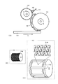
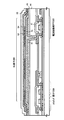
上記課題を達成するために、本発明ではEL層を印刷法により形成することを特徴とする。印刷法としては、凸版印刷法又はスクリーン印刷法を用いることができるが、特に凸版印刷法が好ましい。ここで本発明において凸版印刷法を用いる場合について図1を用いて説明する。
【0008】
図1に示したのは、本発明で用いる凸版印刷用装置の一部である。図1において、110はアニロックスロール、111はドクターバー(ドクターブレードともいう)であり、ドクターバー111によりEL材料と溶媒との混合物(以下、EL形成物という)112がアニロックスロール110の表面付近に溜められている。なお、ここでいうEL材料とは蛍光性有機化合物であり、一般的に正孔注入層、正孔輸送層、発光層、電子輸送層もしくは電子注入層と呼ばれている有機化合物を指す。
【0009】
アニロックスロール110の表面には図1(B)に示すようにメッシュ状の溝(以下、メッシュという)110aが設けられており、矢印Aの方向に回転することでメッシュ110aがEL形成物112を表面に保持していく。なお、アニロックスロール110の表面に図示された点線はEL形成物が保持されていることを意味している。
【0010】
そして、113は印刷ロール、114は凸版であり、凸版114はエッチング等により表面に凹凸が形成されている。この様子を図1(C)に示す。図1(C)の場合、1枚の基板上に複数枚のEL表示装置を作製するために凸版114には画素部用パターン114aが複数箇所に形成されている。さらに、画素部用パターン114aを拡大すると、複数の画素に対応する位置に凸部114bが形成されている。
【0011】
前述のアニロックスロール110は回転しながらメッシュ110aにEL形成物112を保持し続ける。一方、印刷ロール113は矢印Bの方向に回転し、凸版114の凸部114bのみがメッシュ110aと接触する。この時、凸部114bの表面にEL形成物112が塗布される。
【0012】
そして、印刷ロール113と同じ速度で水平移動(矢印Cの方向)する基板115と凸部114bが接した箇所にEL形成物112が印刷される。これにより基板115上にはEL形成物112がマトリクス状に配列された状態で印刷されることになる。
【0013】
その後、真空中での加熱処理によりEL形成物112に含まれる溶媒を気化させてEL材料を残す。このため、溶媒はEL材料のガラス転移温度(Tg)よりも低い温度で気化するものを用いる必要がある。また、EL形成物の粘度により最終的に形成されるEL層の膜厚が決まる。この場合、溶媒の選定により粘度を調節することができるが、粘度は10〜50cp(好ましくは20〜30cp)が好ましい。
【0014】
さらに、EL形成物112中に結晶核となりうる不純物が多いと、溶媒を気化させる際にEL材料が結晶化してしまう可能性が高くなる。結晶化してしまうと発光効率が落ちるため好ましくなく、できるだけEL形成物112の中には不純物が含まれないようにすることが望ましい。
【0015】
不純物を低減するには、溶媒の精製時、EL材料の精製時、又は溶媒とEL材料を混合する時の環境を可能な限り清浄化しておくことも重要であるが、図1のような印刷用装置によりEL形成物を印刷する際の雰囲気にも注意することが好ましい。具体的には、上記EL形成物の印刷工程を、窒素もしくは希ガスなどの不活性ガスが充填された室内(代表的にはクリーンブース内)に設置された印刷用装置で行うことが望ましい。
【0016】
この祭、不活性ガスを充填した室内は大気圧状態もしくは加圧状態(典型的には2〜5気圧、好ましくは2〜3気圧)に保持しておけば良い。本発明を実施した場合、EL材料を成膜するにあたって真空蒸着装置のような真空排気設備を必要とする装置を必要としないため、設備が簡易になるとともにメンテナンスも容易なものとなる利点がある。
【0017】
なお、本発明はアクティブマトリクス型EL表示装置にもパッシブマトリクス型(単純マトリクス型)EL表示装置にも実施することができる。
【0018】
【発明の実施の形態】
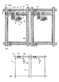
本発明の実施の形態について、図2、図3を用いて説明する。図2に示したのは本発明であるEL表示装置の画素部の断面図であり、図3(A)はその上面図、図3(B)はその回路構成である。実際には画素がマトリクス状に複数配列されて画素部(画像表示部)が形成される。なお、図3(A)をA−A’で切断した断面図が図2に相当する。従って図2及び図3で共通の符号を用いているので、適宜両図面を参照すると良い。また、図3の上面図では二つの画素を図示しているが、どちらも同じ構造である。
【0019】
図2において、11は基板、12は下地となる絶縁膜(以下、下地膜という)である。基板11としてはガラス基板、ガラスセラミックス基板、石英基板、シリコン基板、セラミックス基板、金属基板若しくはプラスチック基板(プラスチックフィルムも含む)を用いることができる。
【0020】
また、下地膜12は特に可動イオンを含む基板や導電性を有する基板を用いる場合に有効であるが、石英基板には設けなくても構わない。下地膜12としては、珪素(シリコン)を含む絶縁膜を用いれば良い。なお、本明細書において「珪素を含む絶縁膜」とは、具体的には酸化珪素膜、窒化珪素膜若しくは窒化酸化珪素膜(SiOxNyで示される)など珪素、酸素若しくは窒素を所定の割合で含む絶縁膜を指す。
【0021】
また、下地膜12に放熱効果を持たせることにより薄膜トランジスタ(以下、TFTという)の発熱を発散させることはTFTの劣化又はEL素子の劣化を防ぐためにも有効である。放熱効果を持たせるには公知のあらゆる材料を用いることができる。
【0022】
ここでは画素内に二つのTFTを形成している。201はスイッチング用素子として機能するTFT(以下、スイッチング用TFTという)、202はEL素子へ流す電流量を制御する電流制御用素子として機能するTFT(以下、電流制御用TFTという)であり、どちらもnチャネル型TFTで形成されている。
【0023】
nチャネル型TFTの電界効果移動度はpチャネル型TFTの電界効果移動度よりも大きいため、動作速度が早く大電流を流しやすい。また、同じ電流量を流すにもTFTサイズはnチャネル型TFTの方が小さくできる。そのため、nチャネル型TFTを電流制御用TFTとして用いた方が表示部の有効面積が広くなるので好ましい。
【0024】
pチャネル型TFTはホットキャリア注入が殆ど問題にならず、オフ電流値が低いといった利点があって、スイッチング用TFTとして用いる例や電流制御用TFTとして用いる例が既に報告されている。しかしながら本発明では、LDD領域の位置を異ならせた構造とすることでnチャネル型TFTにおいてもホットキャリア注入の問題とオフ電流値の問題を解決し、全ての画素内のTFT全てをnチャネル型TFTとしている点にも特徴がある。
【0025】
ただし、本発明において、スイッチング用TFTと電流制御用TFTをnチャネル型TFTに限定する必要はなく、両方又はどちらか片方にpチャネル型TFTを用いることも可能である。
【0026】
スイッチング用TFT201は、ソース領域13、ドレイン領域14、LDD領域15a〜15d、高濃度不純物領域16及びチャネル形成領域17a、17bを含む活性層、ゲート絶縁膜18、ゲート電極19a、19b、第1層間絶縁膜20、ソース配線21並びにドレイン配線22を有して形成される。
【0027】
また、図3に示すように、ゲート電極19a、19bは別の材料(ゲート電極19a、19bよりも低抵抗な材料)で形成されたゲート配線211によって電気的に接続されたダブルゲート構造となっている。勿論、ダブルゲート構造だけでなく、トリプルゲート構造などいわゆるマルチゲート構造(直列に接続された二つ以上のチャネル形成領域を有する活性層を含む構造)であっても良い。マルチゲート構造はオフ電流値を低減する上で極めて有効であり、本発明では画素のスイッチング素子201をマルチゲート構造とすることによりオフ電流値の低いスイッチング素子を実現している。
【0028】
また、活性層は結晶構造を含む半導体膜で形成される。即ち、単結晶半導体膜でも良いし、多結晶半導体膜や微結晶半導体膜でも良い。また、ゲート絶縁膜18は珪素を含む絶縁膜で形成すれば良い。また、ゲート電極、ソース配線若しくはドレイン配線としてはあらゆる導電膜を用いることができる。
【0029】
さらに、スイッチング用TFT201においては、LDD領域15a〜15dは、ゲート絶縁膜18を介してゲート電極19a、19bと重ならないように設ける。このような構造はオフ電流値を低減する上で非常に効果的である。
【0030】
なお、チャネル形成領域とLDD領域との間にオフセット領域(チャネル形成領域と同一組成の半導体層でなり、ゲート電圧が印加されない領域)を設けることはオフ電流値を下げる上でさらに好ましい。また、二つ以上のゲート電極を有するマルチゲート構造の場合、チャネル形成領域の間に設けられた高濃度不純物領域がオフ電流値の低減に効果的である。
【0031】
以上のように、マルチゲート構造のTFTを画素のスイッチング素子201として用いることにより、十分にオフ電流値の低いスイッチング素子を実現することができる。そのため、特開平10−189252号公報の図2のようなコンデンサーを設けなくても十分な時間(選択されてから次に選択されるまでの間)電流制御用TFTのゲート電圧を維持しうる。
【0032】
即ち、従来、有効発光面積を狭める要因となっていたコンデンサーを排除することが可能となり、有効発光面積を広くすることが可能となる。このことはEL表示装置の画質を明るくできることを意味する。
【0033】
次に、電流制御用TFT202は、ソース領域31、ドレイン領域32、LDD領域33及びチャネル形成領域34を含む活性層、ゲート絶縁膜18、ゲート電極35、第1層間絶縁膜20、ソース配線36並びにドレイン配線37を有して形成される。なお、ゲート電極35はシングルゲート構造となっているが、マルチゲート構造であっても良い。
【0034】
図2に示すように、スイッチング用TFTのドレインは電流制御用TFTのゲートに接続されている。具体的には電流制御用TFT202のゲート電極35はスイッチング用TFT201のドレイン領域14とドレイン配線(接続配線とも言える)22を介して電気的に接続されている。また、ソース配線36は電流供給線212に接続される。
【0035】
電流制御用TFT202はEL素子203に注入される電流量を制御するための素子であるが、EL素子の劣化を考慮するとあまり多くの電流を流すことは好ましくない。そのため、電流制御用TFT202に過剰な電流が流れないように、チャネル長(L)は長めに設計することが好ましい。望ましくは一画素あたり0.5〜2μA(好ましくは1〜1.5μA)となるようにする。
【0036】
以上のことを踏まえると、図9に示すように、スイッチング用TFTのチャネル長をL1(但しL1=L1a+L1b)、チャネル幅をW1とし、電流制御用TFTのチャネル長をL2、チャネル幅をW2とした時、W1は0.1〜5μm(代表的には0.5〜2μm)、W2は0.5〜10μm(代表的には2〜5μm)とするのが好ましい。また、L1は0.2〜18μm(代表的には2〜15μm)、L2は1〜50μm(代表的には10〜30μm)とするのが好ましい。但し、本発明は以上の数値に限定されるものではない。
【0037】
これらの数値範囲とすることによりVGAクラスの画素数(640×480)を有するEL表示装置からハイビジョンクラスの画素数(1920×1080又は1280×1024)を有するEL表示装置まで、あらゆる規格を網羅することができる。
【0038】
また、スイッチング用TFT201に形成されるLDD領域の長さ(幅)は0.5〜3.5μm、代表的には2.0〜2.5μmとすれば良い。
【0039】
また、図2に示したEL表示装置は、電流制御用TFT202において、ドレイン領域32とチャネル形成領域34との間にLDD領域33が設けられ、且つ、LDD領域33がゲート絶縁膜18を挟んでゲート電極35に重なっている領域と重なっていない領域とを有する点にも特徴がある。
【0040】
電流制御用TFT202は、EL素子204を発光させるための電流を供給すると同時に、その供給量を制御して階調表示を可能とする。そのため、電流を流しても劣化しないようにホットキャリア注入による劣化対策を講じておく必要がある。また、黒色を表示する際は、電流制御用TFT202をオフ状態にしておくが、その際、オフ電流値が高いときれいな黒色表示ができなくなり、コントラストの低下等を招く。従って、オフ電流値も抑える必要がある。
【0041】
ホットキャリア注入による劣化に関しては、ゲート電極に対してLDD領域が重なった構造が非常に効果的であることが知られている。しかしながら、LDD領域全体をゲート電極に重ねてしまうとオフ電流値が増加してしまうため、本出願人はゲート電極に重ならないLDD領域を直列に設けるという新規な構造によって、ホットキャリア対策とオフ電流値対策とを同時に解決している。
【0042】
この時、ゲート電極に重なったLDD領域の長さは0.1〜3μm(好ましくは0.3〜1.5μm)にすれば良い。長すぎては寄生容量を大きくしてしまい、短すぎてはホットキャリアを防止する効果が弱くなってしまう。また、ゲート電極に重ならないLDD領域の長さは1.0〜3.5μm(好ましくは1.5〜2.0μm)にすれば良い。長すぎると十分な電流を流せなくなり、短すぎるとオフ電流値を低減する効果が弱くなる。
【0043】
また、上記構造においてゲート電極とLDD領域とが重なった領域では寄生容量が形成されてしまうため、ソース領域31とチャネル形成領域34との間には設けない方が好ましい。電流制御用TFTはキャリア(ここでは電子)の流れる方向が常に同一であるので、ドレイン領域側のみにLDD領域を設けておけば十分である。
【0044】
但し、電流制御用TFT202の駆動電圧(ソース領域とドレイン領域との間にかかる電圧)が10V以下となるとホットキャリア注入は殆ど問題にならなくなってくるため、LDD領域33を省略することも可能である。その場合、活性層はソース領域31、ドレイン領域32およびチャネル形成領域34からなる。
【0045】
また、流しうる電流量を多くするという観点から見れば、電流制御用TFT202の活性層(特にチャネル形成領域)の膜厚を厚くする(好ましくは50〜100nm、さらに好ましくは60〜80nm)ことも有効である。逆に、スイッチング用TFT201の場合はオフ電流値を小さくするという観点から見れば、活性層(特にチャネル形成領域)の膜厚を薄くする(好ましくは20〜50nm、さらに好ましくは25〜40nm)ことも有効である。
【0046】
次に、41は第1パッシベーション膜であり、膜厚は10nm〜1μm(好ましくは200〜500nm)とすれば良い。材料としては、珪素を含む絶縁膜(特に窒化酸化珪素膜又は窒化珪素膜が好ましい)を用いることができる。このパッシベーション膜41は形成されたTFTをアルカリ金属や水分から保護する役割をもつ。最終的にTFTの上方に設けられるEL層にはナトリウム等のアルカリ金属が含まれている。即ち、第1パッシベーション膜41はこれらのアルカリ金属(可動イオン)をTFT側に侵入させない保護層としても働く。
【0047】
また、第1パッシベーション膜41に放熱効果を持たせることでEL層の熱劣化を防ぐことも有効である。但し、図2の構造のEL表示装置は基板11側に光が放射されるため、第1パッシベーション膜41は透光性を有することが必要である。また、EL層として有機材料を用いる場合、酸素との結合により劣化するので、酸素を放出しやすい絶縁膜は用いないことが望ましい。
【0048】
アルカリ金属の透過を妨げ、さらに放熱効果をもつ透光性材料としては、B(ホウ素)、C(炭素)、N(窒素)から選ばれた少なくとも一つの元素と、Al(アルミニウム)、Si(珪素)、P(リン)から選ばれた少なくとも一つの元素とを含む絶縁膜が挙げられる。例えば、窒化アルミニウム(AlxNy)に代表されるアルミニウムの窒化物、炭化珪素(SixCy)に代表される珪素の炭化物、窒化珪素(SixNy)に代表される珪素の窒化物、窒化ホウ素(BxNy)に代表されるホウ素の窒化物、リン化ホウ素(BxPy)に代表されるホウ素のリン化物を用いることが可能である。また、酸化アルミニウム(AlxOy)に代表されるアルミニウムの酸化物は透光性に優れ、熱伝導率が20Wm-1K-1であり、好ましい材料の一つと言える。これらの材料には上記効果だけでなく、水分の侵入を防ぐ効果もある。なお、上記透光性材料において、x、yは任意の整数である。
【0049】
なお、上記化合物に他の元素を組み合わせることもできる。例えば、酸化アルミニウムに窒素を添加して、AlNxOyで示される窒化酸化アルミニウムを用いることも可能である。この材料にも放熱効果だけでなく、水分やアルカリ金属等の侵入を防ぐ効果がある。なお、上記窒化酸化アルミニウムにおいて、x、yは任意の整数である。
【0050】
また、特開昭62−90260号公報に記載された材料を用いることができる。即ち、Si、Al、N、O、Mを含む絶縁膜(但し、Mは希土類元素の少なくとも一種、好ましくはCe(セリウム),Yb(イッテルビウム),Sm(サマリウム),Er(エルビウム),Y(イットリウム)、La(ランタン)、Gd(ガドリニウム)、Dy(ジスプロシウム)、Nd(ネオジウム)から選ばれた少なくとも一つの元素)を用いることもできる。これらの材料にも放熱効果だけでなく、水分やアルカリ金属等の侵入を防ぐ効果がある。
【0051】
また、少なくともダイヤモンド薄膜又はアモルファスカーボン膜(特にダイヤモンドに特性の近いもの、ダイヤモンドライクカーボン等と呼ばれる。)を含む炭素膜を用いることもできる。これらは非常に熱伝導率が高く、放熱層として極めて有効である。但し、膜厚が厚くなると褐色を帯びて透過率が低下するため、なるべく薄い膜厚(好ましくは5〜100nm)で用いることが好ましい。
【0052】
なお、第1パッシベーション膜41の目的はあくまでアルカリ金属や水分からTFTを保護することにあるので、その効果を損なうものであってはならない。従って、上記放熱効果をもつ材料からなる薄膜を単体で用いることもできるが、これらの薄膜と、アルカリ金属や水分の透過を妨げうる絶縁膜(代表的には窒化珪素膜(SixNy)や窒化酸化珪素膜(SiOxNy))とを積層することは有効である。なお、上記窒化珪素膜又は窒化酸化珪素膜において、x、yは任意の整数である。
【0053】
第1パッシベーション膜41の上には、各TFTを覆うような形で第2層間絶縁膜(平坦化膜と言っても良い)44を形成し、TFTによってできる段差の平坦化を行う。第2層間絶縁膜44としては、有機樹脂膜が好ましく、ポリイミド、ポリアミド、アクリル、BCB(ベンゾシクロブテン)等を用いると良い。勿論、十分な平坦化が可能であれば、無機膜を用いても良い。
【0054】
第2層間絶縁膜44によってTFTによる段差を平坦化することは非常に重要である。後に形成されるEL層は非常に薄いため、段差が存在することによって発光不良を起こす場合がある。従って、EL層をできるだけ平坦面に形成しうるように画素電極を形成する前に平坦化しておくことが望ましい。
【0055】
また、45は第2パッシベーション膜であり、EL素子から拡散するアルカリ金属をブロッキングする重要な役割を担う。膜厚は5nm〜1μm(典型的には20〜300nm)とすれば良い。この第2パッシベーション膜45は、アルカリ金属の透過を妨げうる絶縁膜を用いる。材料としては、第1パッシベーション膜41として用いた材料を用いることができる。
【0056】
また、この第2パッシベーション膜45はEL素子で発生した熱を逃がしてEL素子に熱が蓄積しないように機能する放熱層としても機能する。また、第2層間絶縁膜44が有機樹脂膜である場合は熱に弱いため、EL素子で発生した熱が第2層間絶縁膜44に悪影響を与えないようにする。
【0057】
前述のようにEL表示装置を作製するにあたってTFTを有機樹脂膜で平坦化することは有効であるが、EL素子で発生した熱による有機樹脂膜の劣化を考慮した構造は従来なかった。本発明では第2パッシベーション膜45を設けることによってその点を解決している点も特徴の一つと言える。
【0058】
また、第2パッシベーション膜45は上記熱による劣化を防ぐと同時に、EL層中のアルカリ金属がTFT側へと拡散しないようにするための保護層としても機能し、さらにはEL層側へTFT側から水分や酸素が侵入しないようにする保護層としても機能する。
【0059】
このようにTFT側とEL素子側とを放熱効果が高く、且つ、水分やアルカリ金属の透過を妨げうる絶縁膜で分離するという点は本発明の重要な特徴の一つであり、従来のEL表示装置にはない構成であると言える。
【0060】
また、46は透明導電膜でなる画素電極(EL素子の陽極)であり、第2パッシベーション膜45、第2層間絶縁膜44及び第1パッシベーション膜41にコンタクトホール(開孔)を開けた後、形成された開孔部において電流制御用TFT202のドレイン配線37に接続されるように形成される。
【0061】
次にEL層(厳密には画素電極に接するEL層)47が印刷法により形成される。EL層47は単層又は積層構造で用いられるが、積層構造で用いられる場合が多い。しかし積層する場合は印刷法と気相法(特に蒸着法が好ましい)とを組み合わせることが望ましい。印刷法では溶媒とEL材料とを混合して印刷するので、下地に有機材料があると再び溶解してしまう恐れがある。
【0062】
従って、EL層47のうち画素電極に直接触れる層を印刷法で形成し、それ以降は気相法で形成することが好ましい。勿論、下層のEL材料が溶解しない溶媒を用いて印刷することができれば全ての層を印刷法で形成することもできる。画素電極に直接触れる層としては、正孔注入層、正孔輸送層又は発光層がありえるが、いずれの層を形成する場合においても本発明を用いることができる。
【0063】
本発明ではEL層の形成方法として印刷法を用いるため、EL材料としてはポリマー系材料を用いるのが好ましい。代表的なポリマー系材料としては、ポリパラフェニレンビニレン(PPV)系、ポリビニルカルバゾール(PVK)系、ポリフルオレン系などの高分子材料が挙げられる。
【0064】
ポリマー系材料でなる正孔注入層、正孔輸送層又は発光層を印刷法で形成するには、ポリマー前駆体の状態で印刷し、それを真空中で加熱することによりポリマー系材料でなるEL材料に転化する。そして、その上に蒸着法等で必要なEL材料を積層して積層型のEL層を形成する。
【0065】
具体的には、正孔輸送層としては、ポリマー前駆体であるポリテトラヒドロチオフェニルフェニレンを用い、加熱によりポリフェニレンビニレンとすることが好ましい。膜厚は30〜100nm(好ましくは40〜80nm)とすれば良い。また、発光層としては、赤色発光層にはシアノポリフェニレンビニレン、緑色発光層にはポリフェニレンビニレン、青色発光層にはポリフェニレンビニレン若しくはポリアルキルフェニレンが好ましい。膜厚は30〜150nm(好ましくは40〜100nm)とすれば良い。
【0066】
また、画素電極とその上に形成されるEL材料との間に銅フタルシアニンをバッファ層として設けることも有効である。
【0067】
但し、以上の例は本発明のEL材料として用いることのできる有機EL材料の一例であって、これに限定する必要はまったくない。本発明ではEL材料と溶媒との混合物を印刷して、溶媒を気化させて除去することによりEL層を形成する。従って、溶媒を気化させる際にEL層のガラス転移温度を超えない組み合わせであれば如何なるEL材料を用いても良い。
【0068】
代表的には溶媒としてクロロフォルム、ジクロロメタン、γブチルラクトン、ブチルセルソルブ又はNMP(N−メチル−2−ピロリドン)といった有機溶媒を用いても良いし、水を用いても良い。また、EL形成物の粘度を上げるための添加剤を加えることも有効である。
【0069】
また、EL層47を形成する際、処理雰囲気は極力水分の少ない乾燥雰囲気とし、不活性ガス中で行うことが望ましい。EL層は水分や酸素の存在によって容易に劣化してしまうため、形成する際は極力このような要因を排除しておく必要がある。例えば、乾燥した窒素雰囲気、乾燥したアルゴン雰囲気等が好ましい。そのためには、印刷用装置を、不活性ガスを充填した室内(本実施例ではクリーンブース内)に設置し、その雰囲気中で印刷処理を行うことが望ましい。
【0070】
この祭、不活性ガスを充填した室内は大気圧状態もしくは加圧状態(典型的には2〜5気圧、好ましくは2〜3気圧)に保持しておけば良い。本発明を実施した場合、EL材料を成膜するにあたって真空蒸着装置のような真空排気設備を必要とする装置を必要としないため、設備が簡易になるとともにメンテナンスも容易なものとなる利点がある。
【0071】
以上のようにしてEL層47を印刷法により形成したら、次に陰極48、保護電極49が形成される。これら陰極48、保護電極49は真空蒸着法で形成すればよい。また、陰極48と保護電極49を大気解放しないで連続的に形成することによりEL層の劣化をさらに抑制することができる。また、本明細書中では、画素電極(陽極)、EL層及び陰極で形成される発光素子をEL素子と呼ぶ。
【0072】
陰極48としては、仕事関数の小さいマグネシウム(Mg)、リチウム(Li)若しくはカルシウム(Ca)を含む材料を用いる。好ましくはMgAg(MgとAgをMg:Ag=10:1で混合した材料)でなる電極を用いれば良い。他にもMgAgAl電極、LiAl電極、また、LiFAl電極が挙げられる。また、保護電極49は陰極48を外部の水分等から保護膜するために設けられる電極であり、アルミニウム(Al)若しくは銀(Ag)を含む材料が用いられる。この保護電極49には放熱効果もある。
【0073】
なお、EL層47及び陰極48は大気解放せずに乾燥された不活性雰囲気中にて連続的に形成することが望ましい。これはEL層として有機材料を用いる場合、水分に非常に弱いため、大気解放した時の吸湿を避けるためである。さらに、EL層47及び陰極48だけでなく、その上の保護電極49まで連続形成するとさらに良い。
【0074】
また、図2の構造はRGBのいずれかに対応した一種類のEL素子を形成する単色発光方式を用いた場合の例である。なお、図2には一つの画素しか図示していないが、画素部には同一構造の複数の画素がマトリクス状に配列されている。なお、RGBのいずれかに対応したEL層は公知の材料を採用すれば良い。
【0075】
また、上記方式以外にも、白色発光のEL素子とカラーフィルターを組み合わせた方式、青色又は青緑発光のEL素子と蛍光体(蛍光性の色変換層:CCM)とを組み合わせた方式、陰極(対向電極)に透明電極を使用してRGBに対応したEL素子を重ねる方式等を用いてカラー表示を行うこともできる。勿論、白色発光のEL層を単層で形成して白黒表示を行うことも可能である。
【0076】
また、50は第3パッシベーション膜であり、膜厚は10nm〜1μm(好ましくは200〜500nm)とすれば良い。第3パッシベーション膜50を設ける目的は、EL層47を水分から保護する目的が主であるが、第2パッシベーション膜45と同様に放熱効果をもたせても良い。従って、形成材料としては第1パッシベーション膜41と同様のものを用いることができる。但し、EL層47として有機材料を用いる場合、酸素との結合により劣化する可能性があるので、酸素を放出しやすい絶縁膜は用いないことが望ましい。
【0077】
また、上述のようにEL層は熱に弱いので、なるべく低温(好ましくは室温から120℃までの温度範囲)で成膜するのが望ましい。従って、プラズマCVD法、スパッタ法、真空蒸着法、イオンプレーティング法又は溶液塗布法(スピンコーティング法)が望ましい成膜方法と言える。
【0078】
このように、第2パッシベーション膜45を設けるだけでも十分にEL素子の劣化を抑制することはできるが、さらに好ましくはEL素子を第2パッシベーション膜45及び第3パッシベーション膜50というようにEL素子を挟んで形成された二層の絶縁膜によって囲み、EL層への水分、酸素の侵入を防ぎ、EL層からのアルカリ金属の拡散を防ぎ、EL層への熱の蓄積を防ぐ。その結果、EL層の劣化がさらに抑制されて信頼性の高いEL表示装置が得られる。
【0079】
また、本発明のEL表示装置は図2のような構造の画素からなる画素部を有し、画素内において機能に応じて構造の異なるTFTが配置されている。これによりオフ電流値の十分に低いスイッチング用TFTと、ホットキャリア注入に強い電流制御用TFTとが同じ画素内に形成でき、高い信頼性を有し、且つ、良好な画像表示が可能な(動作性能の高い)EL表示装置が得られる。
【0080】
なお、図2の画素構造においてスイッチング用TFTとしてマルチゲート構造のTFTを用いているが、LDD領域の配置等の構成に関しては図2の構成に限定する必要はない。
【0081】
また、ここでは基板面に半導体素子としてTFTを設け、TFTに電気的に接続されたEL素子を形成する際に本発明を実施した例を示したが、半導体素子としてシリコン基板面に形成されたトランジスタ(MOSFETと呼ばれる)を用いた場合にも本発明を実施することができる。
【0082】
以上の構成でなる本発明について、以下に示す実施例でもってさらに詳細な説明を行うこととする。
【0083】
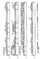
〔実施例1〕
本発明の実施例について図4〜図6を用いて説明する。ここでは、画素部とその周辺に設けられる駆動回路部のTFTを同時に作製する方法について説明する。但し、説明を簡単にするために、駆動回路に関しては基本回路であるCMOS回路を図示することとする。
【0084】
まず、図4(A)に示すように、ガラス基板300上に下地膜301を300nmの厚さに形成する。本実施例では下地膜301として窒化酸化珪素膜を積層して用いる。この時、ガラス基板300に接する方の窒素濃度を10〜25wt%としておくと良い。
【0085】
また、下地膜301の一部として、図2に示した第1パッシベーション膜41と同様の材料からなる絶縁膜を設けることは有効である。電流制御用TFTは大電流を流すことになるので発熱しやすく、なるべく近いところに放熱効果のある絶縁膜を設けておくことは有効である。
【0086】
次に下地膜301の上に50nmの厚さの非晶質珪素膜(図示せず))を公知の成膜法で形成する。なお、非晶質珪素膜に限定する必要はなく、非晶質構造を含む半導体膜(微結晶半導体膜を含む)であれば良い。さらに非晶質シリコンゲルマニウム膜などの非晶質構造を含む化合物半導体膜でも良い。また、膜厚は20〜100nmの厚さであれば良い。
【0087】
そして、公知の技術により非晶質珪素膜を結晶化し、結晶質珪素膜(多結晶シリコン膜若しくはポリシリコン膜ともいう)302を形成する。公知の結晶化方法としては、電熱炉を使用した熱結晶化方法、レーザー光を用いたレーザーアニール結晶化法、赤外光を用いたランプアニール結晶化法がある。本実施例では、XeClガスを用いたエキシマレーザー光を用いて結晶化する。
【0088】
なお、本実施例では線状に加工したパルス発振型のエキシマレーザー光を用いるが、矩形であっても良いし、連続発振型のアルゴンレーザー光や連続発振型のエキシマレーザー光を用いることもできる。
【0089】
本実施例では結晶質珪素膜をTFTの活性層として用いるが、非晶質珪素膜を用いることも可能である。しかし、電流制御用TFTの面積をできるだけ小さくして画素の開口率を高めるには電流を流しやすい結晶質珪素膜を用いた方が有利である。
【0090】
なお、オフ電流を低減する必要のあるスイッチング用TFTの活性層を非晶質珪素膜で形成し、電流制御用TFTの活性層を結晶質珪素膜で形成することは有効である。非晶質珪素膜はキャリア移動度が低いため電流を流しにくくオフ電流が流れにくい。即ち、電流を流しにくい非晶質珪素膜と電流を流しやすい結晶質珪素膜の両者の利点を生かすことができる。
【0091】
次に、図4(B)に示すように、結晶質珪素膜302上に酸化珪素膜でなる保護膜303を130nmの厚さに形成する。この厚さは100〜200nm(好ましくは130〜170nm)の範囲で選べば良い。また、珪素を含む絶縁膜であれば他の膜でも良い。この保護膜303は不純物を添加する際に結晶質珪素膜が直接プラズマに曝されないようにするためと、微妙な濃度制御を可能にするために設ける。
【0092】
そして、その上にレジストマスク304a、304bを形成し、保護膜303を介してn型を付与する不純物元素(以下、n型不純物元素という)を添加する。なお、n型不純物元素としては、代表的には15族に属する元素、典型的にはリン又は砒素を用いることができる。なお、本実施例ではフォスフィン(PH3)を質量分離しないでプラズマ励起したプラズマドーピング法を用い、リンを1×10¹⁸atoms/cm3の濃度で添加する。勿論、質量分離を行うイオンインプランテーション法を用いても良い。
【0093】
この工程により形成されるn型不純物領域305、306には、n型不純物元素が2×10¹⁶〜5×10¹⁹atoms/cm3(代表的には5×1017〜5×1018atoms/cm3)の濃度で含まれるようにドーズ量を調節する。
【0094】
次に、図4(C)に示すように、保護膜303を除去し、添加した15族に属する元素の活性化を行う。活性化手段は公知の技術を用いれば良いが、本実施例ではエキシマレーザー光の照射により活性化する。勿論、パルス発振型でも連続発振型でも良いし、エキシマレーザー光に限定する必要はない。但し、添加された不純物元素の活性化が目的であるので、結晶質珪素膜が溶融しない程度のエネルギーで照射することが好ましい。なお、保護膜303をつけたままレーザー光を照射しても良い。
【0095】
なお、このレーザー光による不純物元素の活性化に際して、熱処理による活性化を併用しても構わない。熱処理による活性化を行う場合は、基板の耐熱性を考慮して450〜550℃程度の熱処理を行えば良い。
【0096】
この工程によりn型不純物領域305、306の端部、即ち、n型不純物領域305、306の周囲に存在するn型不純物元素を添加していない領域との境界部(接合部)が明確になる。このことは、後にTFTが完成した時点において、LDD領域とチャネル形成領域とが非常に良好な接合部を形成しうることを意味する。
【0097】
次に、図4(D)に示すように、結晶質珪素膜の不要な部分を除去して、島状の半導体膜(以下、活性層という)307〜310を形成する。
【0098】
次に、図4(E)に示すように、活性層307〜310を覆ってゲート絶縁膜311を形成する。ゲート絶縁膜311としては、10〜200nm、好ましくは50〜150nmの厚さの珪素を含む絶縁膜を用いれば良い。これは単層構造でも積層構造でも良い。本実施例では110nm厚の窒化酸化珪素膜を用いる。
【0099】
次に、200〜400nm厚の導電膜を形成し、パターニングしてゲート電極312〜316を形成する。なお、本実施例ではゲート電極と、ゲート電極に電気的に接続された引き回しのための配線(以下、ゲート配線という)とを別の材料で形成する。具体的にはゲート電極よりも低抵抗な材料をゲート配線として用いる。これは、ゲート電極としては微細加工が可能な材料を用い、ゲート配線には微細加工はできなくとも配線抵抗が小さい材料を用いるためである。勿論、ゲート電極とゲート配線とを同一材料で形成してしまっても構わない。
【0100】
また、ゲート電極は単層の導電膜で形成しても良いが、必要に応じて二層、三層といった積層膜とすることが好ましい。ゲート電極の材料としては公知のあらゆる導電膜を用いることができる。ただし、上述のように微細加工が可能、具体的には2μm以下の線幅にパターニング可能な材料が好ましい。
【0101】
代表的には、タンタル(Ta)、チタン(Ti)、モリブデン(Mo)、タングステン(W)、クロム(Cr)、シリコン(Si)から選ばれた元素でなる膜、または前記元素の窒化物膜(代表的には窒化タンタル膜、窒化タングステン膜、窒化チタン膜)、または前記元素を組み合わせた合金膜(代表的にはMo−W合金、Mo−Ta合金)、または前記元素のシリサイド膜(代表的にはタングステンシリサイド膜、チタンシリサイド膜)を用いることができる。勿論、単層で用いても積層して用いても良い。
【0102】
本実施例では、50nm厚の窒化タングステン(WN)膜と、350nm厚のタングステン(W)膜とでなる積層膜を用いる。これはスパッタ法で形成すれば良い。また、スパッタガスとしてXe、Ne等の不活性ガスを添加すると応力による膜はがれを防止することができる。
【0103】
またこの時、ゲート電極313、316はそれぞれn型不純物領域305、306の一部とゲート絶縁膜311を挟んで重なるように形成する。この重なった部分が後にゲート電極と重なったLDD領域となる。
【0104】
次に、図5(A)に示すように、ゲート電極312〜316をマスクとして自己整合的にn型不純物元素(本実施例ではリン)を添加する。こうして形成される不純物領域317〜323にはn型不純物領域305、306の1/2〜1/10(代表的には1/3〜1/4)の濃度でリンが添加されるように調節する。具体的には、1×1016〜5×1018atoms/cm3(典型的には3×1017〜3×1018atoms/cm3)の濃度が好ましい。
【0105】
次に、図5(B)に示すように、ゲート電極等を覆う形でレジストマスク324a〜324dを形成し、n型不純物元素(本実施例ではリン)を添加して高濃度にリンを含む不純物領域325〜331を形成する。ここでもフォスフィン(PH3)を用いたイオンドープ法で行い、この領域のリンの濃度は1×10²⁰〜1×10²¹atoms/cm3(代表的には2×1020〜5×1020atoms/cm3)となるように調節する。
【0106】
この工程によってnチャネル型TFTのソース領域若しくはドレイン領域が形成されるが、スイッチング用TFTでは、図5(A)の工程で形成したn型不純物領域320〜322の一部を残す。この残された領域が、図2におけるスイッチング用TFTのLDD領域15a〜15dに対応する。
【0107】
次に、図5(C)に示すように、レジストマスク324a〜324dを除去し、新たにレジストマスク332を形成する。そして、p型不純物元素(本実施例ではボロン)を添加し、高濃度にボロンを含む不純物領域333、334を形成する。ここではジボラン(B2H6)を用いたイオンドープ法により3×10²⁰〜3×10²¹atoms/cm3(代表的には5×1020〜1×1021atoms/cm3ノ)濃度となるようにボロンを添加する。
【0108】
なお、不純物領域333、334には既に1×10¹⁶〜5×10¹⁸atoms/cm3の濃度でリンが添加されているが、ここで添加されるボロンはその少なくとも3倍以上の濃度で添加される。そのため、予め形成されていたn型の不純物領域は完全にP型に反転し、P型の不純物領域として機能する。
【0109】
次に、レジストマスク332を除去した後、それぞれの濃度で添加されたn型またはp型不純物元素を活性化する。活性化手段としては、ファーネスアニール法、レーザーアニール法、またはランプアニール法で行うことができる。本実施例では電熱炉において窒素雰囲気中、550℃、4時間の熱処理を行う。
【0110】
このとき雰囲気中の酸素を極力排除することが重要である。なぜならば酸素が少しでも存在していると露呈したゲート電極の表面が酸化され、抵抗の増加を招くと共に後にオーミックコンタクトを取りにくくなるからである。従って、上記活性化工程における処理雰囲気中の酸素濃度は1ppm以下、好ましくは0.1ppm以下とすることが望ましい。
【0111】
次に、活性化工程が終了したら300nm厚のゲート配線335を形成する。ゲート配線335の材料としては、アルミニウム(Al)又は銅(Cu)を主成分(組成として50〜100%を占める。)とする金属膜を用いれば良い。配置としては図3のゲート配線211のように、スイッチング用TFTのゲート電極314、315(図3のゲート電極19a、19bに相当する)を電気的に接続するように形成する。(図5(D))
【0112】
このような構造とすることでゲート配線の配線抵抗を非常に小さくすることができるため、面積の大きい画像表示領域(画素部)を形成することができる。即ち、画面の大きさが対角10インチ以上(さらには30インチ以上)のEL表示装置を実現する上で、本実施例の画素構造は極めて有効である。
【0113】
次に、図6(A)に示すように、第1層間絶縁膜336を形成する。第1層間絶縁膜336としては、珪素を含む絶縁膜を単層で用いるか、その中で組み合わせた積層膜を用いれば良い。また、膜厚は400nm〜1.5μmとすれば良い。本実施例では、200nm厚の窒化酸化珪素膜の上に800nm厚の酸化珪素膜を積層した構造とする。
【0114】
さらに、3〜100%の水素を含む雰囲気中で、300〜450℃で1〜12時間の熱処理を行い水素化処理を行う。この工程は熱的に励起された水素により半導体膜の不対結合手を水素終端する工程である。水素化の他の手段として、プラズマ水素化(プラズマにより励起された水素を用いる)を行っても良い。
【0115】
なお、水素化処理は第1層間絶縁膜336を形成する間に入れても良い。即ち、200nm厚の窒化酸化珪素膜を形成した後で上記のように水素化処理を行い、その後で残り800nm厚の酸化珪素膜を形成しても構わない。
【0116】
次に、第1層間絶縁膜336に対してコンタクトホールを形成し、ソース配線337〜340と、ドレイン配線341〜343を形成する。なお、本実施例ではこの電極を、チタン膜を100nm、チタンを含むアルミニウム膜を300nm、チタン膜150nmをスパッタ法で連続形成した3層構造の積層膜とする。勿論、他の導電膜でも良い。
【0117】
次に、50〜500nm(代表的には200〜300nm)の厚さで第1パッシベーション膜344を形成する。本実施例では第1パッシベーション膜344として300nm厚の窒化酸化珪素膜を用いる。これは窒化珪素膜で代用しても良い。勿論、図2の第1パッシベーション膜41と同様の材料を用いることが可能である。
【0118】
なお、窒化酸化珪素膜の形成に先立ってH2、NH3等水素を含むガスを用いてプラズマ処理を行うことは有効である。この前処理により励起された水素が第1層間絶縁膜336に供給され、熱処理を行うことで、第1パッシベーション膜344の膜質が改善される。それと同時に、第1層間絶縁膜336に添加された水素が下層側に拡散するため、効果的に活性層を水素化することができる。
【0119】
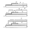
次に、図6(B)に示すように有機樹脂からなる第2層間絶縁膜347を形成する。有機樹脂としてはポリイミド、ポリアミド、アクリル、BCB(ベンゾシクロブテン)等を使用することができる。特に、第2層間絶縁膜347は平坦化の意味合いが強いので、平坦性に優れたアクリルが好ましい。本実施例ではTFTによって形成される段差を十分に平坦化しうる膜厚でアクリル膜を形成する。好ましくは1〜5μm(さらに好ましくは2〜4μm)とすれば良い。
【0120】
次に、第2層間絶縁膜347上に100nm厚の第2パッシベーション膜348を形成する。本実施例ではSi、Al、N、O及びLaを含む絶縁膜を用いるため、その上に設けられるEL層からのアルカリ金属の拡散を防止することができる。また、同時にEL層に水分を侵入させず、且つ、EL層で発生した熱を分散させて、熱によるEL層の劣化や平坦化膜(第2層間絶縁膜)の劣化を抑制することができる。
【0121】
そして、第2パッシベーション膜348、第2層間絶縁膜347及び第1パッシベーション膜344にドレイン配線343に達するコンタクトホールを形成し、画素電極349を形成する。本実施例では酸化インジウム・スズ(ITO)膜を110nmの厚さに形成し、パターニングを行って画素電極とする。この画素電極349がEL素子の陽極となる。なお、他の材料として、酸化インジウム・チタン膜やITOに酸化亜鉛を混合した膜を用いることも可能である。
【0122】
なお、本実施例では画素電極349がドレイン配線343を介して電流制御用TFTのドレイン領域331へと電気的に接続された構造となっている。この構造には次のような利点がある。
【0123】
画素電極349はEL層(発光層)や電荷輸送層などの有機材料に直接接することになるため、EL層等に含まれた可動イオンが画素電極中を拡散する可能性がある。即ち、本実施例の構造は画素電極349を直接活性層の一部であるドレイン領域331へ接続せず、ドレイン配線343を中継することによって活性層中への可動イオンの侵入を防ぐことができる。
【0124】
次に、図6(C)に示すように、EL層350を、図1を用いて説明した凸版印刷法により形成し、さらに蒸着法により陰極(MgAg電極)351及び保護電極352を大気解放しないで形成する。このときEL層350及び陰極351を形成するに先立って画素電極349に対して熱処理を施し、水分を完全に除去しておくことが望ましい。なお、本実施例ではEL素子の陰極としてMgAg電極を用いるが、公知の他の材料であっても良い。
【0125】
なお、EL層350としては【発明の実施の形態】の欄で説明した材料を用いることができる。本実施例では正孔輸送層(Hole transporting layer)及び発光層(Emitting layer)でなる2層構造をEL層とするが、正孔注入層、電子注入層若しくは電子輸送層のいずれかを設ける場合もある。このように組み合わせは既に様々な例が報告されており、そのいずれの構成を用いても構わない。
【0126】
本実施例では正孔輸送層としてポリマー前駆体であるポリテトラヒドロチオフェニルフェニレンを印刷法により形成し、加熱によりポリフェニレンビニレンとする。また、発光層としては、ポリビニルカルバゾールに1,3,4−オキサジアゾール誘導体のPBDを30〜40%分子分散させたものを蒸着法により形成し、緑色の発光中心としてクマリン6を約1%添加している。
【0127】
また、保護電極352でもEL層350を水分や酸素から保護することは可能であるが、さらに好ましくは第3パッシベーション膜353を設けると良い。本実施例では第3パッシベーション膜353として300nm厚の窒化珪素膜を設ける。この第3パッシベーション膜も保護電極352の後に大気解放しないで連続的に形成しても構わない。勿論、第3パッシベーション膜353としては、図2の第3パッシベーション膜50と同一の材料を用いることができる。
【0128】
また、保護電極352はMgAg電極351の劣化を防ぐために設けられ、アルミニウムを主成分とする金属膜が代表的である。勿論、他の材料でも良い。また、EL層350、MgAg電極351は非常に水分に弱いので、保護電極352までを大気解放しないで連続的に形成し、外気からEL層を保護することが望ましい。
【0129】
なお、EL層350の膜厚は10〜400nm(典型的には60〜150nm、好ましくは100〜120nm)、MgAg電極351の厚さは80〜200nm(典型的には100〜150nm)とすれば良い。
【0130】
こうして図6(C)に示すような構造のアクティブマトリクス型EL表示装置が完成する。ところで、本実施例のアクティブマトリクス型EL表示装置は、画素部だけでなく駆動回路部にも最適な構造のTFTを配置することにより、非常に高い信頼性を示し、動作特性も向上しうる。
【0131】
まず、極力動作速度を落とさないようにホットキャリア注入を低減させる構造を有するTFTを、駆動回路を形成するCMOS回路のnチャネル型TFT205として用いる。なお、ここでいう駆動回路としては、シフトレジスタ、バッファ、レベルシフタ、サンプリング回路(サンプル及びホールド回路)などが含まれる。デジタル駆動を行う場合には、D/Aコンバータなどの信号変換回路も含まれうる。
【0132】
本実施例の場合、図6(C)に示すように、nチャネル型TFT205の活性層は、ソース領域355、ドレイン領域356、LDD領域357及びチャネル形成領域358を含み、LDD領域357はゲート絶縁膜311を挟んでゲート電極313と重なっている。
【0133】
ドレイン領域側のみにLDD領域を形成しているのは、動作速度を落とさないための配慮である。また、このnチャネル型TFT205はオフ電流値をあまり気にする必要はなく、それよりも動作速度を重視した方が良い。従って、LDD領域357は完全にゲート電極に重ねてしまい、極力抵抗成分を少なくすることが望ましい。即ち、いわゆるオフセットはなくした方がよい。
【0134】
また、CMOS回路のpチャネル型TFT206は、ホットキャリア注入による劣化が殆ど気にならないので、特にLDD領域を設けなくても良い。勿論、nチャネル型TFT205と同様にLDD領域を設け、ホットキャリア対策を講じることも可能である。
【0135】
なお、駆動回路の中でもサンプリング回路は他の回路と比べて少し特殊であり、チャネル形成領域を双方向に大電流が流れる。即ち、ソース領域とドレイン領域の役割が入れ替わるのである。さらに、オフ電流値を極力低く抑える必要があり、そういった意味でスイッチング用TFTと電流制御用TFTの中間程度の機能を有するTFTを配置することが望ましい。
【0136】
従って、サンプリング回路を形成するnチャネル型TFTは、図10に示すような構造のTFTを配置することが望ましい。図10に示すように、LDD領域901a、901bの一部がゲート絶縁膜902を介してゲート電極903と重なる。この効果は電流制御用TFT202の説明で述べた通りであり、サンプリング回路の場合はチャネル形成領域904を挟む形で設ける点が異なる。
【0137】
なお、実際には図6(C)まで完成したら、さらに外気に曝されないように気密性が高く、脱ガスの少ない保護フィルム(ラミネートフィルム、紫外線硬化樹脂フィルム等)やセラミックス製シーリングカンなどのハウジング材でパッケージング(封入)することが好ましい。その際、ハウジング材の内部を不活性雰囲気にしたり、内部に吸湿性材料(例えば酸化バリウム)を配置することでEL層の信頼性(寿命)が向上する。
【0138】
また、パッケージング等の処理により気密性を高めたら、基板上に形成された素子又は回路から引き回された端子と外部信号端子とを接続するためのコネクター(フレキシブルプリントサーキット:FPC)を取り付けて製品として完成する。このような出荷できる状態にまでしたEL表示装置を本明細書中ではELモジュールという。
【0139】
ここで本実施例のアクティブマトリクス型EL表示装置の構成を図7の斜視図を用いて説明する。本実施例のアクティブマトリクス型EL表示装置は、ガラス基板601上に形成された、画素部602と、ゲート側駆動回路603と、ソース側駆動回路604で構成される。画素部のスイッチング用TFT605はnチャネル型TFTであり、ゲート側駆動回路603に接続されたゲート配線606、ソース側駆動回路604に接続されたソース配線607の交点に配置されている。また、スイッチング用TFT605のドレインは電流制御用TFT608のゲートに接続されている。
【0140】
さらに、電流制御用TFT608のソース側は電流供給線609に接続され、電流制御用TFT608のドレインにはEL素子610が接続されている。
【0141】
そして、外部入出力端子となるFPC611には駆動回路まで信号を伝達するための入出力配線(接続配線)612、613、及び電流供給線609に接続された入出力配線614が設けられている。
【0142】
また、図7に示したEL表示装置の回路構成の一例を図8に示す。本実施例のEL表示装置は、ソース側駆動回路701、ゲート側駆動回路(A)707、ゲート側駆動回路(B)711、画素部706を有している。なお、本明細書中において、駆動回路とはソース側処理回路およびゲート側駆動回路を含めた総称である。
【0143】
ソース側駆動回路701は、シフトレジスタ702、レベルシフタ703、バッファ704、サンプリング回路(サンプル及びホールド回路)705を備えている。また、ゲート側駆動回路(A)707は、シフトレジスタ708、レベルシフタ709、バッファ710を備えている。ゲート側駆動回路(B)711も同様な構成である。
【0144】
ここでシフトレジスタ702、708は駆動電圧が5〜16V(代表的には10V)であり、回路を形成するCMOS回路に使われるnチャネル型TFTは図6(C)の205で示される構造が適している。
【0145】
また、レベルシフタ703、709、バッファ704、710はシフトレジスタと同様に、図6(C)のnチャネル型TFT205を含むCMOS回路が適している。なお、ゲート配線をダブルゲート構造、トリプルゲート構造といったマルチゲート構造とすることは、各回路の信頼性を向上させる上で有効である。
【0146】
また、サンプリング回路705はソース領域とドレイン領域が反転する上、オフ電流値を低減する必要があるので、図10のnチャネル型TFT208を含むCMOS回路が適している。
【0147】
また、画素部706は図2に示した構造の画素を配置する。
【0148】
なお、上記構成は、図4〜6に示した作製工程に従ってTFTを作製することによって容易に実現することができる。また、本実施例では画素部と駆動回路の構成のみ示しているが、本実施例の作製工程に従えば、その他にも信号分割回路、D/Aコンバータ回路、オペアンプ回路、γ補正回路など駆動回路以外の論理回路を同一基板上に形成することが可能であり、さらにはメモリ部やマイクロプロセッサ等を形成しうると考えている。
【0149】
さらに、ハウジング材をも含めた本実施例のELモジュールについて図11(A)、(B)を用いて説明する。なお、必要に応じて図7、図8で用いた符号を引用することにする。
【0150】
基板(TFTの下の下地膜を含む)1700上には画素部1701、ソース側駆動回路1702、ゲート側駆動回路1703が形成されている。それぞれの駆動回路からの各種配線は、入出力配線612〜614を経てFPC611に至り外部機器へと接続される。
【0151】
このとき少なくとも画素部、好ましくは駆動回路及び画素部を囲むようにしてハウジング材1704を設ける。なお、ハウジング材1704は画素部1701の外寸(高さ)よりも内寸(奥行き)が大きい凹部を有する形状又はシート形状であり、接着剤1705によって、基板1700と共同して密閉空間を形成するようにして基板1700に固着される。このとき、EL素子は完全に前記密閉空間に封入された状態となり、外気から完全に遮断される。なお、ハウジング材1704は複数設けても構わない。
【0152】
また、ハウジング材1704の材質はガラス、ポリマー等の絶縁性物質が好ましい。例えば、非晶質ガラス(硼硅酸塩ガラス、石英等)、結晶化ガラス、セラミックスガラス、有機系樹脂(アクリル系樹脂、スチレン系樹脂、ポリカーボネート系樹脂、エポキシ系樹脂等)、シリコーン系樹脂が挙げられる。また、セラミックスを用いても良い。また、接着剤1705が絶縁性物質であるならステンレス合金等の金属材料を用いることも可能である。
【0153】
また、接着剤1705の材質は、エポキシ系樹脂、アクリレート系樹脂等の接着剤を用いることが可能である。さらに、熱硬化性樹脂や光硬化性樹脂を接着剤として用いることもできる。但し、可能な限り酸素、水分を透過しない材質であることが必要である。
【0154】
さらに、ハウジング材と基板1700との間の空隙1706は不活性ガス(アルゴン、ヘリウム、窒素等)を充填しておくことが望ましい。また、ガスに限らず不活性液体(パーフルオロアルカンに代表されるの液状フッ素化炭素等)を用いることも可能である。不活性液体に関しては特開平8−78159号で用いられているような材料で良い。
【0155】
また、空隙1706に乾燥剤を設けておくことも有効である。乾燥剤としては特開平9−148066号公報に記載されているような材料を用いることができる。典型的には酸化バリウムを用いれば良い。
【0156】
また、図11(B)に示すように、画素部には個々に孤立したEL素子を有する複数の画素が設けられ、それらは全て保護電極1707を共通電極として有している。本実施例では、EL層、陰極(MgAg電極)及び保護電極を大気解放しないで連続形成することが好ましいとしたが、EL層と陰極とを同じマスク材を用いて形成し、保護電極だけ別のマスク材で形成すれば図11(B)の構造を実現することができる。
【0157】
このとき、EL層と陰極は画素部のみ設ければよく、駆動回路の上に設ける必要はない。勿論、駆動回路上に設けられていても問題とはならないが、EL層にアルカリ金属が含まれていることを考慮すると設けない方が好ましい。
【0158】
なお、保護電極1707は1708で示される領域において、入出力配線1709に接続される。入出力配線1709は保護電極1707に所定の電圧(本実施例では接地電位、具体的には0V)を与えるための配線であり、導電性ペースト材料1710を介してFPC611に接続される。
【0159】
ここで領域1708におけるコンタクト構造を実現するための作製工程について図12を用いて説明する。
【0160】
まず、本実施例の工程に従って図6(A)の状態を得る。このとき、基板端部(図11(B)において1708で示される領域)において第1層間絶縁膜336及びゲート絶縁膜311を除去し、その上に入出力配線1709を形成する。勿論、図6(A)のソース配線及びドレイン配線と同時に形成される。(図12(A))
【0161】
次に、図6(B)において第2パッシベーション膜348、第2層間絶縁膜347及び第1パッシベーション膜344をエッチングする際に、1801で示される領域を除去し、且つ開孔部1802を形成する。(図12(B))
【0162】
この状態で画素部ではEL素子の形成工程(画素電極、EL層及び陰極の形成工程)が行われる。この際、図12に示される領域ではマスク材を用いてEL素子が形成されないようにする。そして、陰極351を形成した後、別のマスク材を用いて保護電極352を形成する。これにより保護電極352と入出力配線1709とが電気的に接続される。さらに、第3パッシベーション膜353を設けて図12(C)の状態を得る。
【0163】
以上の工程により図11(B)の1708で示される領域のコンタクト構造が実現される。そして、入出力配線1709はハウジング材1704と基板1700との間を隙間(但し接着剤1705で充填されている。即ち、接着剤1705は入出力配線の段差を十分に平坦化しうる厚さが必要である。)を通ってFPC611に接続される。なお、ここでは入出力配線1709について説明したが、他の出力配線612〜614も同様にしてハウジング材1704の下を通ってFPC611に接続される。
【0164】
〔実施例2〕
本実施例では、画素の構成を図3(B)に示した構成と異なるものとした例を図13に示す。
【0165】
本実施例では、図3(B)に示した二つの画素を、接地電位を与えるための電流供給線212について対称となるように配置する。即ち、図13に示すように、電流供給線212を隣接する二つの画素間で共通化することで、必要とする配線の本数を低減することができる。なお、画素内に配置されるTFT構造等はそのままで良い。
【0166】
このような構成とすれば、より高精細な画素部を作製することが可能となり、画像の品質が向上する。
【0167】
なお、本実施例の構成は実施例1の作製工程に従って容易に実現可能であり、TFT構造等に関しては実施例1や図2の説明を参照すれば良い。
【0168】
〔実施例3〕
本実施例では、図2と異なる構造の画素部を形成する場合について図14を用いて説明する。なお、第2層間絶縁膜44を形成する工程までは実施例1に従えば良い。また、第2層間絶縁膜44で覆われたスイッチング用TFT201、電流制御用TFT202は図1と同じ構造であるので、ここでの説明は省略する。
【0169】
本実施例の場合、第2パッシベーション膜45、第2層間絶縁膜44及び第1パッシベーション膜41に対してコンタクトホールを形成したら、画素電極51を形成した後、陰極52及びEL層53を形成する。本実施例では陰極52を真空蒸着法で形成した後、乾燥された不活性雰囲気を維持したまま凸版印刷法又はスクリーン印刷法によりEL層53を形成する。
【0170】
本実施例では画素電極51として、150nm厚のアルミニウム合金膜(1wt%のチタンを含有したアルミニウム膜)を設ける。なお、画素電極の材料としては金属材料であれば如何なる材料でも良いが、反射率の高い材料であることが好ましい。また、陰極52として120nm厚のMgAg電極を用い、EL層53の膜厚は120nmとする。
【0171】
本実施例ではポリビニルカルバゾールに1,3,4−オキサジアゾール誘導体のPBDを30〜40%分子分散させ、発光中心としてクマリン6を約1%添加したものをEL材料とし、それに溶媒を混合させてEL形成物を作製する。そして、そのEL形成物を凸版印刷法又はスクリーン印刷法により塗布してベーク処理を行い、50nm厚の緑色の発光層を得る。そして、その上に70nm厚のTPDを蒸着法により形成し、EL層53を得る。
【0172】
次に、透明導電膜(本実施例ではITO膜)でなる陽極54を110nmの厚さに形成する。こうしてEL素子209が形成され、実施例1に示した材料でもって第3パッシベーション膜55を形成すれば図14に示すような構造の画素が完成する。
【0173】
本実施例の構造とした場合、各画素で生成された緑色の光はTFTが形成された基板とは反対側に放射される。そのため、画素内のほぼ全域、即ちTFTが形成された領域をも有効な発光領域として用いることができる。その結果、画素の有効発光面積が大幅に向上し、画像の明るさやコントラスト比(明暗の比)が向上する。
【0174】
なお、本実施例の構成は、実施例1、2のいずれの構成とも自由に組み合わせることが可能である。
【0175】
〔実施例4〕
実施例1〜4ではトップゲート型TFTの場合について説明したが、本発明はTFT構造に限定されるものではないので、ボトムゲート型TFT(代表的には逆スタガ型TFT)を用いて実施しても構わない。また、逆スタガ型TFTは如何なる手段で形成されたものでも良い。
【0176】
逆スタガ型TFTは工程数がトップゲート型TFTよりも少なくし易い構造であるため、本発明の課題である製造コストの低減には非常に有利である。なお、本実施例の構成は、実施例2、3のいずれの構成とも自由に組み合わせることが可能である。
【0177】
〔実施例5〕
実施例1の図6(C)又は図2の構造において、活性層と基板との間に設けられる下地膜として、第2パッシベーション膜45と同様に放熱効果の高い材料を用いることは有効である。特に電流制御用TFTは長時間電流を流すことになるため発熱しやすく、自己発熱による劣化が問題となりうる。そのような場合に、本実施例のように下地膜が放熱効果を有することでTFTの熱劣化を防ぐことができる。
【0178】
もちろん、基板から拡散する可動イオン等から防ぐ効果も重要であるので、第1パッシベーション膜41と同様にSi、Al、N、O、Mを含む化合物と珪素を含む絶縁膜との積層構造を用いることも好ましい。
【0179】
なお、本実施例の構成は、実施例1〜4のいずれの構成とも自由に組み合わせることが可能である。
【0180】
〔実施例6〕
実施例3に示した画素構造とした場合、EL層から発する光は基板とは反対側に放射されるため、基板と画素電極との間に存在する絶縁膜等の透過率を気にする必要がない。即ち、多少透過率の低い材料であっても用いることができる。
【0181】
従って、下地膜12、第1パッシベーション膜41又は第2パッシベーション膜45としてダイヤモンド薄膜又はアモルファスカーボン膜と呼ばれる炭素膜を用いる上で有利である。即ち、透過率の低下を気にする必要がないため、膜厚を100〜500nmというように厚く設定することができ、放熱効果をより高めることが可能である。
【0182】
なお、第3パッシベーション膜50に上記炭素膜を用いる場合に関しては、やはり透過率の低下は避けるべきであるので、膜厚は5〜100nm程度にしておくことが好ましい。
【0183】
なお、本実施例においても下地膜12、第1パッシベーション膜41、第2パッシベーション膜45又は第3パッシベーション膜50のいずれに炭素膜を用いる場合においても、他の絶縁膜と積層して用いることは有効である。
【0184】
なお、本実施例は実施例3に示した画素構造とする場合において特に有効であるが、実施例1、2、4もしくは5のいずれの構成とも自由に組み合わせることが可能である。
【0185】
〔実施例7〕
本発明ではEL表示装置の画素においてスイッチング用TFTをマルチゲート構造とすることによりスイッチング用TFTのオフ電流値を低減し、保持容量の必要性を排除している。これは保持容量の専有する面積を発光領域として有効に活用するための工夫である。
【0186】
しかしながら、保持容量を完全になくせないまでも専有面積を小さくするだけで有効発光面積を広げるという効果は得られる。即ち、スイッチング用TFTをマルチゲート構造にすることによりオフ電流値を低減し、保持容量の専有面積を縮小化するだけでも十分である。
【0187】
その場合、図15に示すように、スイッチング用TFT201のドレインに対して電流制御用TFT202のゲートと並列に保持容量1401を形成しても構わない。
【0188】
なお、本実施例の構成は、実施例1〜6のいずれの構成とも自由に組み合わせることができる。即ち、画素内に保持容量が設けられるだけであって、TFT構造やEL層の材料等に限定を加えるものではない。
【0189】
〔実施例8〕
実施例1では、結晶質珪素膜302の形成手段としてレーザー結晶化を用いているが、本実施例では異なる結晶化手段を用いる場合について説明する。
【0190】
本実施例では、非晶質珪素膜を形成した後、特開平7−130652号公報に記載された技術を用いて結晶化を行う。同公報に記載された技術は、結晶化を促進(助長)する触媒として、ニッケル等の元素を用い、結晶性の高い結晶質珪素膜を得る技術である。
【0191】
また、結晶化工程が終了した後で、結晶化に用いた触媒を除去する工程を行っても良い。その場合、特開平10−270363号若しくは特開平8−330602号に記載された技術により触媒をゲッタリングすれば良い。
【0192】
また、本出願人による特願平11−076967の出願明細書に記載された技術を用いてTFTを形成しても良い。
【0193】
以上のように、実施例1に示した作製工程は一実施例であって、図2又は実施例1の図6(C)の構造が実現できるのであれば、他の作製工程を用いても問題はない。
【0194】
なお、本実施例の構成は、実施例1〜7のいずれの構成とも自由に組み合わせることが可能である。
【0195】
〔実施例9〕
本発明のEL表示装置を駆動するにあたって、画像信号としてアナログ信号を用いたアナログ駆動を行うこともできるし、デジタル信号を用いたデジタル駆動を行うこともできる。
【0196】
アナログ駆動を行う場合、スイッチング用TFTのソース配線にはアナログ信号が送られ、その階調情報を含んだアナログ信号が電流制御用TFTのゲート電圧となる。そして、電流制御用TFTでEL素子に流れる電流を制御し、EL素子の発光強度を制御して階調表示を行う。なお、アナログ駆動を行う場合は電流制御用TFTを飽和領域で動作させると良い。
【0197】
一方、デジタル駆動を行う場合、アナログ的な階調表示とは異なり、時分割駆動と呼ばれる階調表示を行う。即ち、発光時間の長さを調節することで、視覚的に色階調が変化しているように見せる。なお、デジタル駆動を行う場合は電流制御用TFTを線形領域で動作させると良い。
【0198】
EL素子は液晶素子に比べて非常に応答速度が速いため、高速で駆動することが可能である。そのため、1フレームを複数のサブフレームに分割して階調表示を行う時分割駆動に適した素子であると言える。
【0199】
このように、本発明は素子構造に関する技術であるので、駆動方法は如何なるものであっても構わない。
【0200】
〔実施例10〕
実施例1ではEL層として有機EL材料を用いることが好ましいとしたが、本発明は無機EL材料を用いても実施できる。但し、現在の無機EL材料は非常に駆動電圧が高いため、アナログ駆動を行う場合には、そのような駆動電圧に耐えうる耐圧特性を有するTFTを用いなければならない。
【0201】
または、将来的にさらに駆動電圧の低い無機EL材料が開発されれば、本発明に適用することは可能である。
【0202】
また、本実施例の構成は、実施例1〜9のいずれの構成とも自由に組み合わせることが可能である。
【0203】
〔実施例11〕
本発明を実施して形成されたアクティブマトリクス型EL表示装置(ELモジュール)は、自発光型であるため液晶表示装置に比べて明るい場所での視認性に優れている。そのため直視型のELディスプレイ(ELモジュールを組み込んだ表示ディスプレイを指す)として用途は広い。
【0204】
なお、ELディスプレイが液晶ディスプレイよりも有利な点の一つとして視野角の広さが挙げられる。従って、TV放送等を大画面で鑑賞するには対角30インチ以上(典型的には40インチ以上)の表示ディスプレイ(表示モニタ)として本発明のELディスプレイを用いるとよい。
【0205】
また、ELディスプレイ(パソコンモニタ、TV放送受信用モニタ、広告表示モニタ等)として用いるだけでなく、様々な電子装置の表示ディスプレイとして用いることができる。
【0206】
その様な電子装置としては、ビデオカメラ、デジタルカメラ、ゴーグル型ディスプレイ(ヘッドマウントディスプレイ)、カーナビゲーション、パーソナルコンピュータ、携帯情報端末(モバイルコンピュータ、携帯電話または電子書籍等)、記録媒体を備えた画像再生装置(具体的にはコンパクトディスク(CD)、レーザーディスク(LD)又はデジタルバーサタイルディスク(DVD)等の記録媒体を再生し、その画像を表示しうるディスプレイを備えた装置)などが挙げられる。それら電子装置の例を図16に示す。
【0207】
図16(A)はパーソナルコンピュータであり、本体2001、筐体2002、表示部2003、キーボード2004を含む。本発明は表示部2003に用いることができる。
【0208】
図16(B)はビデオカメラであり、本体2101、表示部2102、音声入力部2103、操作スイッチ2104、バッテリー2105、受像部2106を含む。本発明を表示部2102に用いることができる。
【0209】
図16(C)は頭部取り付け型のELディスプレイの一部(右片側)であり、本体2201、信号ケーブル2202、頭部固定バンド2203、表示モニタ2204、光学系2205、表示装置2206を含む。本発明は表示装置2206に用いることができる。
【0210】
図16(D)は記録媒体を備えた画像再生装置(具体的にはDVD再生装置)であり、本体2301、記録媒体(CD、LDまたはDVD等)2302、操作スイッチ2303、表示部(a)2304、表示部(b)2305を含む。表示部(a)は主として画像情報を表示し、表示部(b)は主として文字情報を表示するが、本発明はこれら表示部(a)、(b)に用いることができる。なお、記録媒体を備えた画像再生装置としては、CD再生装置、ゲーム機器などに本発明を用いることができる。
【0211】
図16(E)は携帯型(モバイル)コンピュータであり、本体2401、カメラ部2402、受像部2403、操作スイッチ2404、表示部2405を含む。本発明は表示部2405に用いることができる。
【0212】
図16(F)はELディスプレイであり、筐体2501、支持台2502、表示部2503を含む。本発明は表示部2503に用いることができる。ELディスプレイは視野角が広いため液晶ディスプレイに比べて大画面化した場合において有利であり、対角10インチ以上(特に対角30インチ以上)のディスプレイにおいて有利である。
【0213】
また、将来的にEL材料の発光輝度が高くなれば、出力した画像情報を含む光をレンズ等で拡大投影してフロント型若しくはリア型のプロジェクターに用いることも可能となる。
【0214】
以上の様に、本発明の適用範囲は極めて広く、あらゆる分野の電子装置に適用することが可能である。また、本実施例の電子装置は実施例1〜10を自由に組み合わせて実現することができる。
【0215】
【発明の効果】
本発明を用いることで、EL層の形成を非常に安価に行うことができる。そのため、EL表示装置を作製する製造コストが低減される。
【0216】
また、EL層とTFTとの間にアルカリ金属の透過を妨げうる絶縁膜を設けることによりEL層からアルカリ金属が拡散してTFT特性に悪影響を与えることを防ぐことができる。その結果、EL表示装置の動作性能や信頼性を大幅に向上させることができる。
【0217】
また、安価に製造しうるEL表示装置を表示ディスプレイとして用いることで電子装置の製造コストが低減される。また、上記動作性能や信頼性を向上させたEL表示装置を用いることで、画像品質が良く、耐久性のある(信頼性の高い)応用製品(電子装置)を生産することが可能となる。
【図面の簡単な説明】
【図1】 凸版印刷法の原理を説明するための図。
【図2】 EL表示装置の画素部の断面構造を示す図。
【図3】 EL表示装置の画素部の上面構造及び構成を示す図。
【図4】 アクティブマトリクス型EL表示装置の作製工程を示す図。
【図5】 アクティブマトリクス型EL表示装置の作製工程を示す図。
【図6】 アクティブマトリクス型EL表示装置の作製工程を示す図。
【図7】 ELモジュールの外観を示す図。
【図8】 EL表示装置の回路ブロック構成を示す図。
【図9】 EL表示装置の画素部を拡大した図。
【図10】 EL表示装置のサンプリング回路の素子構造を示す図。
【図11】 ELモジュールの外観と断面構造を示す図。
【図12】 コンタクト構造の作製工程を示す図。
【図13】 EL表示装置の画素部の構成を示す図。
【図14】 EL表示装置の画素部の断面構造を示す図。
【図15】 EL表示装置の画素部の構成を示す図。
【図16】 電子装置の具体例を示す図。[0001]
BACKGROUND OF THE INVENTION
The present invention displays an electro-optical device typified by an EL (electroluminescence) display device formed by forming a semiconductor element (an element using a semiconductor thin film, typically a thin film transistor) on a substrate, and the electro-optical device. The present invention relates to an electronic device (electronic device) having a display. In particular, it relates to a manufacturing method thereof.
[0002]
[Prior art]
In recent years, a technique for forming a thin film transistor (hereinafter referred to as TFT) on a substrate has greatly advanced, and application development to an active matrix display device has been advanced. In particular, a TFT using a polysilicon film has higher field-effect mobility than a TFT using a conventional amorphous silicon film, and thus can operate at high speed. For this reason, it is possible to control a pixel, which has been conventionally performed by a drive circuit outside the substrate, with a drive circuit formed on the same substrate as the pixel.
[0003]
Such an active matrix display device has various advantages such as a reduction in manufacturing cost, a reduction in size of the display device, an increase in yield, and a reduction in throughput by forming various circuits and elements on the same substrate. It is attracting attention as.
[0004]
In the active matrix EL display device, each pixel is provided with a switching element made of a TFT, and a driving element that controls current is operated by the switching element to cause the EL layer (light emitting layer) to emit light. For example, there is an EL display device described in US Pat. No. 5,684,365 (see Japanese Laid-Open Publication No. 8-234683) and Japanese Laid-Open Publication No. 10-189252.
[0005]
Various methods for forming the EL layer have been proposed. Examples thereof include a vacuum deposition method, a sputtering method, a spin coating method, a roll coating method, a casting method, an LB method, an ion plating method, a dipping method, and an ink jet method.
[0006]
[Problems to be solved by the invention]
An object of the present invention is to reduce the manufacturing cost of an EL layer, and to provide an inexpensive EL display device. And it makes it a subject to reduce the product cost of the electronic device (electronic device) which has it as a display for a display.
[0007]
[Means for Solving the Problems]
In order to achieve the above object, the present invention is characterized in that an EL layer is formed by a printing method. As the printing method, a relief printing method or a screen printing method can be used, and the relief printing method is particularly preferable. Here, the case where the relief printing method is used in the present invention will be described with reference to FIG.
[0008]
FIG. 1 shows a part of the relief printing apparatus used in the present invention. In FIG. 1, 110 is an anilox roll, 111 is a doctor bar (also referred to as a doctor blade), and a mixture of an EL material and a solvent (hereinafter referred to as EL formation) 112 is brought near the surface of the
[0009]
As shown in FIG. 1B, a mesh-shaped groove (hereinafter referred to as a mesh) 110a is provided on the surface of the
[0010]
[0011]
The
[0012]
Then, the EL formed
[0013]
Thereafter, the solvent contained in the
[0014]
Furthermore, if there are many impurities that can be crystal nuclei in the
[0015]
In order to reduce impurities, it is also important to clean as much as possible the environment during the purification of the solvent, the purification of the EL material, or the mixing of the solvent and the EL material. It is preferable to pay attention to the atmosphere when the EL formed product is printed by the printing apparatus. Specifically, it is desirable to perform the printing process of the EL formed product with a printing apparatus installed in a room (typically in a clean booth) filled with an inert gas such as nitrogen or a rare gas.
[0016]
During this festival, the room filled with an inert gas may be kept at atmospheric pressure or pressurized (typically 2 to 5 atm, preferably 2 to 3 atm). When the present invention is carried out, there is an advantage that the equipment is simplified and the maintenance is easy because an apparatus such as a vacuum vapor deposition apparatus that requires an evacuation facility is not required when depositing the EL material. .
[0017]
Note that the present invention can be applied to both an active matrix type EL display device and a passive matrix type (simple matrix type) EL display device.
[0018]
DETAILED DESCRIPTION OF THE INVENTION
An embodiment of the present invention will be described with reference to FIGS. 2 is a cross-sectional view of a pixel portion of an EL display device according to the present invention, FIG. 3A is a top view thereof, and FIG. 3B is a circuit configuration thereof. Actually, a plurality of pixels are arranged in a matrix to form a pixel portion (image display portion). Note that a cross-sectional view taken along line AA ′ in FIG. 3A corresponds to FIG. Accordingly, since the same reference numerals are used in FIG. 2 and FIG. 3, both drawings should be referred to as appropriate. Further, in the top view of FIG. 3, two pixels are illustrated, but both have the same structure.
[0019]
In FIG. 2, 11 is a substrate, and 12 is an insulating film (hereinafter referred to as a base film) serving as a base. As the
[0020]
The
[0021]
In addition, it is effective to prevent the deterioration of the TFT or the EL element by causing the thin film transistor (hereinafter referred to as TFT) to emit heat by providing the
[0022]
Here, two TFTs are formed in the pixel.
[0023]
Since the field effect mobility of the n-channel TFT is larger than that of the p-channel TFT, the operation speed is high and a large current is likely to flow. Even when the same amount of current flows, the n-channel TFT can be made smaller in TFT size. Therefore, it is preferable to use an n-channel TFT as a current control TFT because the effective area of the display portion is widened.
[0024]
The p-channel TFT has the advantage that hot carrier injection is hardly a problem and has a low off-current value, and examples of using it as a switching TFT and an example of using it as a current control TFT have already been reported. However, the present invention solves the problem of hot carrier injection and the problem of off-current value even in the n-channel TFT by adopting a structure where the positions of the LDD regions are different, and all the TFTs in all the pixels are n-channel type. Another characteristic is that it is a TFT.
[0025]
However, in the present invention, the switching TFT and the current control TFT need not be limited to n-channel TFTs, and p-channel TFTs can be used for both or one of them.
[0026]
The switching
[0027]
As shown in FIG. 3, the
[0028]
The active layer is formed of a semiconductor film including a crystal structure. That is, a single crystal semiconductor film, a polycrystalline semiconductor film, or a microcrystalline semiconductor film may be used. The
[0029]
Further, in the switching
[0030]
Note that it is more preferable to provide an offset region (a region made of a semiconductor layer having the same composition as the channel formation region to which no gate voltage is applied) between the channel formation region and the LDD region in order to reduce the off-state current value. In the case of a multi-gate structure having two or more gate electrodes, a high-concentration impurity region provided between channel formation regions is effective in reducing the off-current value.
[0031]
As described above, a switching element having a sufficiently low off-state current value can be realized by using a TFT having a multi-gate structure as the switching
[0032]
That is, it is possible to eliminate the capacitor that has been a factor for reducing the effective light emitting area, and it is possible to widen the effective light emitting area. This means that the image quality of the EL display device can be brightened.
[0033]
Next, the
[0034]
As shown in FIG. 2, the drain of the switching TFT is connected to the gate of the current control TFT. Specifically, the
[0035]
The
[0036]
Based on the above, as shown in FIG. 9, the channel length of the switching TFT is L1 (where L1 = L1a + L1b), the channel width is W1, the channel length of the current control TFT is L2, and the channel width is W2. In this case, W1 is preferably 0.1 to 5 μm (typically 0.5 to 2 μm), and W2 is preferably 0.5 to 10 μm (typically 2 to 5 μm). L1 is preferably 0.2 to 18 μm (typically 2 to 15 μm), and L2 is preferably 1 to 50 μm (typically 10 to 30 μm). However, the present invention is not limited to the above numerical values.
[0037]
By setting these numerical ranges, all standards are covered, from EL display devices having the number of VGA class pixels (640 × 480) to EL display devices having the number of high-definition class pixels (1920 × 1080 or 1280 × 1024). be able to.
[0038]
The length (width) of the LDD region formed in the switching
[0039]
In the EL display device shown in FIG. 2, in the
[0040]
The
[0041]
Regarding deterioration due to hot carrier injection, it is known that a structure in which an LDD region overlaps a gate electrode is very effective. However, if the entire LDD region is overlaid on the gate electrode, the off-current value increases. Therefore, the applicant has a novel structure in which LDD regions that do not overlap with the gate electrode are provided in series, thereby preventing hot carriers and off-current. It solves value measures at the same time.
[0042]
At this time, the length of the LDD region overlapping with the gate electrode may be 0.1 to 3 μm (preferably 0.3 to 1.5 μm). If it is too long, the parasitic capacitance is increased, and if it is too short, the effect of preventing hot carriers is weakened. The length of the LDD region that does not overlap with the gate electrode may be 1.0 to 3.5 μm (preferably 1.5 to 2.0 μm). If it is too long, it will not be possible to pass a sufficient current, and if it is too short, the effect of reducing the off current value will be weak.
[0043]
Further, in the above structure, a parasitic capacitance is formed in a region where the gate electrode and the LDD region overlap with each other. Therefore, it is preferable not to provide between the
[0044]
However, when the driving voltage of the current control TFT 202 (voltage applied between the source region and the drain region) becomes 10 V or less, hot carrier injection becomes almost no problem, and therefore the
[0045]
Further, from the viewpoint of increasing the amount of current that can be passed, the thickness of the active layer (especially the channel formation region) of the
[0046]
Next,
[0047]
It is also effective to prevent thermal degradation of the EL layer by providing the
[0048]
As a translucent material that prevents alkali metal from passing through and has a heat dissipation effect, at least one element selected from B (boron), C (carbon), and N (nitrogen), Al (aluminum), Si ( And an insulating film containing at least one element selected from silicon and P (phosphorus). For example, aluminum nitride represented by aluminum nitride (AlxNy), silicon carbide represented by silicon carbide (SixCy), silicon nitride represented by silicon nitride (SixNy), and boron nitride (BxNy) Boron phosphide represented by boron nitride and boron phosphide (BxPy) can be used. In addition, an aluminum oxide typified by aluminum oxide (AlxOy) has excellent translucency and a thermal conductivity of 20 Wm. -1 K -1 It can be said that it is one of the preferable materials. These materials not only have the above effects, but also have an effect of preventing moisture from entering. In the translucent material, x and y are arbitrary integers.
[0049]
In addition, another element can also be combined with the said compound. For example, it is possible to use aluminum nitride oxide represented by AlNxOy by adding nitrogen to aluminum oxide. This material has not only a heat dissipation effect but also an effect of preventing moisture, alkali metal and the like from entering. In the aluminum nitride oxide, x and y are arbitrary integers.
[0050]
Moreover, the material described in Unexamined-Japanese-Patent No. 62-90260 can be used. That is, an insulating film containing Si, Al, N, O, and M (where M is at least one of rare earth elements, preferably Ce (cerium), Yb (ytterbium), Sm (samarium), Er (erbium), Y ( Yttrium), La (lanthanum), Gd (gadolinium), Dy (dysprosium), and Nd (neodymium). These materials have not only a heat dissipation effect but also an effect of preventing intrusion of moisture, alkali metals, and the like.
[0051]
In addition, a carbon film including at least a diamond thin film or an amorphous carbon film (in particular, a material having characteristics close to diamond, called diamond-like carbon) can be used. These have very high thermal conductivity and are extremely effective as a heat dissipation layer. However, as the film thickness increases, the film becomes brownish and the transmittance decreases. Therefore, it is preferable to use the film as thin as possible (preferably 5 to 100 nm).
[0052]
Note that the purpose of the
[0053]
On the
[0054]
It is very important to flatten the step due to the TFT by the second
[0055]
[0056]
The
[0057]
As described above, it is effective to planarize a TFT with an organic resin film in manufacturing an EL display device, but there has not been a structure that takes into account deterioration of an organic resin film due to heat generated in an EL element. It can be said that the present invention solves this problem by providing the
[0058]
In addition, the
[0059]
As described above, the TFT side and the EL element side are separated from each other by an insulating film that has a high heat dissipation effect and can prevent the permeation of moisture and alkali metal. It can be said that this is a configuration that the display device does not have.
[0060]
[0061]
Next, an EL layer (strictly speaking, an EL layer in contact with the pixel electrode) 47 is formed by a printing method. The
[0062]
Therefore, it is preferable to form the layer directly touching the pixel electrode in the
[0063]
In the present invention, since a printing method is used as a method for forming the EL layer, it is preferable to use a polymer material as the EL material. Typical polymer materials include polymer materials such as polyparaphenylene vinylene (PPV), polyvinyl carbazole (PVK), and polyfluorene.
[0064]
In order to form a hole injection layer, a hole transport layer or a light emitting layer made of a polymer material by a printing method, the EL is made of a polymer material by printing in a state of a polymer precursor and heating it in a vacuum. Convert to material. Then, a necessary EL material is stacked thereon by vapor deposition or the like to form a stacked EL layer.
[0065]
Specifically, as the hole transport layer, it is preferable to use polytetrahydrothiophenylphenylene which is a polymer precursor and to polyphenylene vinylene by heating. The film thickness may be 30 to 100 nm (preferably 40 to 80 nm). The light emitting layer is preferably cyanopolyphenylene vinylene for the red light emitting layer, polyphenylene vinylene for the green light emitting layer, and polyphenylene vinylene or polyalkylphenylene for the blue light emitting layer. The film thickness may be 30 to 150 nm (preferably 40 to 100 nm).
[0066]
It is also effective to provide copper phthalocyanine as a buffer layer between the pixel electrode and the EL material formed thereon.
[0067]
However, the above example is an example of the organic EL material that can be used as the EL material of the present invention, and it is not absolutely necessary to limit to this. In the present invention, an EL layer is formed by printing a mixture of an EL material and a solvent and evaporating and removing the solvent. Accordingly, any EL material may be used as long as the combination does not exceed the glass transition temperature of the EL layer when the solvent is vaporized.
[0068]
Typically, an organic solvent such as chloroform, dichloromethane, γ-butyllactone, butyl cellosolve or NMP (N-methyl-2-pyrrolidone) may be used as a solvent, or water may be used. It is also effective to add an additive for increasing the viscosity of the EL formed product.
[0069]
Further, when forming the
[0070]
During this festival, the room filled with an inert gas may be kept at atmospheric pressure or pressurized (typically 2 to 5 atm, preferably 2 to 3 atm). When the present invention is carried out, there is an advantage that the equipment is simplified and the maintenance is easy because an apparatus such as a vacuum vapor deposition apparatus that requires an evacuation facility is not required when depositing the EL material. .
[0071]
After the
[0072]
As the
[0073]
Note that the
[0074]
Further, the structure of FIG. 2 is an example in the case of using a monochromatic light emitting method for forming one kind of EL element corresponding to any of RGB. Although only one pixel is shown in FIG. 2, a plurality of pixels having the same structure are arranged in a matrix in the pixel portion. Note that a known material may be used for the EL layer corresponding to any of RGB.
[0075]
In addition to the above methods, a method combining a white light emitting EL element and a color filter, a method combining a blue or blue-green light emitting EL element and a phosphor (fluorescent color conversion layer: CCM), a cathode ( Color display can also be performed using a method in which transparent elements are used for the counter electrode) and EL elements corresponding to RGB are stacked. Of course, it is also possible to perform monochrome display by forming a white light emitting EL layer as a single layer.
[0076]
[0077]
Further, since the EL layer is vulnerable to heat as described above, it is desirable to form the film at as low a temperature as possible (preferably in a temperature range from room temperature to 120 ° C.). Therefore, the plasma CVD method, the sputtering method, the vacuum deposition method, the ion plating method, or the solution coating method (spin coating method) can be said to be a preferable film forming method.
[0078]
As described above, it is possible to sufficiently suppress the deterioration of the EL element only by providing the
[0079]
Further, the EL display device of the present invention has a pixel portion composed of pixels having a structure as shown in FIG. 2, and TFTs having different structures are arranged in the pixels in accordance with functions. As a result, a switching TFT having a sufficiently low off-current value and a current control TFT resistant to hot carrier injection can be formed in the same pixel, have high reliability, and can display a good image (operation) An EL display device with high performance is obtained.
[0080]
Note that although a multi-gate TFT is used as a switching TFT in the pixel structure of FIG. 2, the arrangement of the LDD region and the like need not be limited to those shown in FIG.
[0081]
In addition, here, an example is shown in which the present invention is implemented when a TFT is provided as a semiconductor element on the substrate surface and an EL element electrically connected to the TFT is formed, but the semiconductor element is formed on the silicon substrate surface. The present invention can also be implemented when a transistor (called a MOSFET) is used.
[0082]
The present invention having the above-described configuration will be described in more detail with the following examples.
[0083]
[Example 1]
An embodiment of the present invention will be described with reference to FIGS. Here, a method for simultaneously manufacturing a TFT of a pixel portion and a driver circuit portion provided around the pixel portion will be described. However, in order to simplify the description, a CMOS circuit, which is a basic circuit, is illustrated with respect to the drive circuit.
[0084]
First, as shown in FIG. 4A, a
[0085]
In addition, it is effective to provide an insulating film made of the same material as the
[0086]
Next, an amorphous silicon film (not shown) having a thickness of 50 nm is formed on the
[0087]
Then, the amorphous silicon film is crystallized by a known technique to form a crystalline silicon film (also referred to as a polycrystalline silicon film or a polysilicon film) 302. Known crystallization methods include a thermal crystallization method using an electric furnace, a laser annealing crystallization method using laser light, and a lamp annealing crystallization method using infrared light. In this embodiment, crystallization is performed using excimer laser light using XeCl gas.
[0088]
In this embodiment, a pulse oscillation type excimer laser beam processed into a linear shape is used. However, a rectangular shape, a continuous oscillation type argon laser beam, or a continuous oscillation type excimer laser beam may be used. .
[0089]
In this embodiment, a crystalline silicon film is used as an active layer of a TFT, but an amorphous silicon film can also be used. However, in order to increase the aperture ratio of the pixel by reducing the area of the current control TFT as much as possible, it is advantageous to use a crystalline silicon film that easily allows current to flow.
[0090]
It is effective to form the active layer of the switching TFT that needs to reduce the off current from an amorphous silicon film, and to form the active layer of the current control TFT from a crystalline silicon film. Since the amorphous silicon film has low carrier mobility, it is difficult for an electric current to flow and an off current is difficult to flow. That is, the advantages of both an amorphous silicon film that hardly allows current to flow and a crystalline silicon film that easily allows current to flow can be utilized.
[0091]
Next, as shown in FIG. 4B, a
[0092]
Then, resist
[0093]
In the n-
[0094]
Next, as shown in FIG. 4C, the
[0095]
Note that activation by heat treatment may be used in combination with the activation of the impurity element by the laser beam. When activation by heat treatment is performed, heat treatment at about 450 to 550 ° C. may be performed in consideration of the heat resistance of the substrate.
[0096]
By this step, the end portion of the n-
[0097]
Next, as shown in FIG. 4D, unnecessary portions of the crystalline silicon film are removed, and island-shaped semiconductor films (hereinafter referred to as active layers) 307 to 310 are formed.
[0098]
Next, as illustrated in FIG. 4E, a
[0099]
Next, a conductive film having a thickness of 200 to 400 nm is formed and patterned to form
[0100]
The gate electrode may be formed of a single-layer conductive film, but it is preferable to form a stacked film of two layers or three layers as necessary. Any known conductive film can be used as the material of the gate electrode. However, a material that can be finely processed as described above, specifically, that can be patterned to a line width of 2 μm or less is preferable.
[0101]
Typically, a film made of an element selected from tantalum (Ta), titanium (Ti), molybdenum (Mo), tungsten (W), chromium (Cr), and silicon (Si), or a nitride film of the element (Typically a tantalum nitride film, a tungsten nitride film, a titanium nitride film), an alloy film (typically, a Mo—W alloy, a Mo—Ta alloy), or a silicide film of the above elements (typical) Specifically, a tungsten silicide film or a titanium silicide film) can be used. Of course, it may be used as a single layer or may be laminated.
[0102]
In this embodiment, a stacked film including a tungsten nitride (WN) film having a thickness of 50 nm and a tungsten (W) film having a thickness of 350 nm is used. This may be formed by sputtering. Further, when an inert gas such as Xe or Ne is added as a sputtering gas, peeling of the film due to stress can be prevented.
[0103]
At this time, the
[0104]
Next, as shown in FIG. 5A, an n-type impurity element (phosphorus in this embodiment) is added in a self-aligning manner using the
[0105]
Next, as shown in FIG. 5B, resist
[0106]
Although the source region or the drain region of the n-channel TFT is formed by this step, the switching TFT leaves a part of the n-
[0107]
Next, as shown in FIG. 5C, the resist
[0108]
Note that the
[0109]
Next, after removing the resist
[0110]
At this time, it is important to eliminate oxygen in the atmosphere as much as possible. This is because the presence of even a small amount of oxygen oxidizes the exposed surface of the gate electrode, which increases resistance and makes it difficult to make ohmic contact later. Therefore, the oxygen concentration in the treatment atmosphere in the activation step is 1 ppm or less, preferably 0.1 ppm or less.
[0111]
Next, when the activation process is completed, a
[0112]
With such a structure, the wiring resistance of the gate wiring can be extremely reduced, so that an image display region (pixel portion) having a large area can be formed. That is, the pixel structure of this embodiment is extremely effective in realizing an EL display device having a screen size of 10 inches or more (or 30 inches or more) diagonally.
[0113]
Next, as shown in FIG. 6A, a first
[0114]
Further, a hydrogenation treatment is performed by performing a heat treatment at 300 to 450 ° C. for 1 to 12 hours in an atmosphere containing 3 to 100% hydrogen. This step is a step in which the dangling bonds of the semiconductor film are terminated with hydrogen by thermally excited hydrogen. As another means of hydrogenation, plasma hydrogenation (using hydrogen excited by plasma) may be performed.
[0115]
Note that the hydrogenation treatment may be performed while the first
[0116]
Next, contact holes are formed in the first
[0117]
Next, a
[0118]
Prior to the formation of the silicon nitride oxide film, H 2 , NH Three It is effective to perform plasma treatment using a gas containing isohydrogen. Hydrogen excited by this pretreatment is supplied to the first
[0119]
Next, as shown in FIG. 6B, a second
[0120]
Next, a
[0121]
Then, a contact hole reaching the
[0122]
In this embodiment, the
[0123]
Since the
[0124]
Next, as shown in FIG. 6C, the
[0125]
Note that the material described in the section of the present invention can be used for the
[0126]
In this embodiment, polytetrahydrothiophenylphenylene, which is a polymer precursor, is formed as a hole transport layer by a printing method, and polyphenylene vinylene is formed by heating. The light-emitting layer is formed by vapor deposition of 30-40% PBD of 1,3,4-oxadiazole derivative in polyvinyl carbazole, and about 1% of coumarin 6 is used as a green emission center. It is added.
[0127]
In addition, the
[0128]
The
[0129]
Note that the thickness of the
[0130]
Thus, an active matrix EL display device having a structure as shown in FIG. 6C is completed. By the way, the active matrix EL display device of this embodiment can provide extremely high reliability and improve the operating characteristics by arranging TFTs having an optimal structure not only in the pixel portion but also in the drive circuit portion.
[0131]
First, a TFT having a structure that reduces hot carrier injection so as not to reduce the operating speed as much as possible is used as an n-channel TFT 205 of a CMOS circuit that forms a driving circuit. Note that the drive circuit here includes a shift register, a buffer, a level shifter, a sampling circuit (sample and hold circuit), and the like. In the case of performing digital driving, a signal conversion circuit such as a D / A converter may be included.
[0132]
In this embodiment, as shown in FIG. 6C, the active layer of the n-channel TFT 205 includes a
[0133]
The reason why the LDD region is formed only on the drain region side is to prevent the operation speed from being lowered. In addition, the n-channel TFT 205 does not need to care about the off-current value, and it is better to focus on the operation speed than that. Therefore, it is desirable that the
[0134]
In addition, since the p-channel TFT 206 of the CMOS circuit is hardly concerned about deterioration due to hot carrier injection, it is not particularly necessary to provide an LDD region. Needless to say, it is possible to provide an LDD region as in the case of the n-channel TFT 205 and take measures against hot carriers.
[0135]
Note that the sampling circuit in the driver circuit is a little special compared to other circuits, and a large current flows in both directions in the channel formation region. That is, the roles of the source region and the drain region are interchanged. Furthermore, it is necessary to keep the off-current value as low as possible, and in that sense, it is desirable to dispose a TFT having an intermediate function between the switching TFT and the current control TFT.
[0136]
Therefore, it is desirable to dispose a TFT having a structure as shown in FIG. 10 as the n-channel TFT forming the sampling circuit. As shown in FIG. 10, part of the
[0137]
Actually, when completed up to FIG. 6C, a housing such as a protective film (laminate film, UV curable resin film, etc.) and a ceramic sealing can with high airtightness and low outgassing so as not to be exposed to the outside air. It is preferable to package (enclose) with a material. At that time, the reliability (life) of the EL layer is improved by making the inside of the housing material an inert atmosphere or disposing a hygroscopic material (for example, barium oxide) inside.
[0138]
In addition, when the airtightness is improved by processing such as packaging, a connector (flexible printed circuit: FPC) for connecting the terminal routed from the element or circuit formed on the substrate and the external signal terminal is attached. Completed as a product. In this specification, an EL display device that can be shipped is referred to as an EL module.
[0139]
Here, the configuration of the active matrix EL display device of this embodiment will be described with reference to the perspective view of FIG. The active matrix EL display device of this embodiment includes a
[0140]
Further, the source side of the
[0141]
The
[0142]
An example of a circuit configuration of the EL display device illustrated in FIG. 7 is illustrated in FIG. The EL display device of this embodiment includes a source side driver circuit 701, a gate side driver circuit (A) 707, a gate side driver circuit (B) 711, and a pixel portion 706. Note that in this specification, the drive circuit is a generic name including a source side processing circuit and a gate side drive circuit.
[0143]
The source side driver circuit 701 includes a shift register 702, a level shifter 703, a buffer 704, and a sampling circuit (sample and hold circuit) 705. The gate side driver circuit (A) 707 includes a
[0144]
Here, the driving voltages of the shift registers 702 and 708 are 5 to 16 V (typically 10 V), and an n-channel TFT used in a CMOS circuit forming the circuit has a structure indicated by 205 in FIG. Is suitable.
[0145]
As the
[0146]
In addition, since the sampling circuit 705 needs to reduce the off current value in addition to the inversion of the source region and the drain region, a CMOS circuit including the n-channel TFT 208 in FIG. 10 is suitable.
[0147]
Further, the pixel portion 706 includes pixels having the structure shown in FIG.
[0148]
In addition, the said structure can be easily implement | achieved by manufacturing TFT according to the manufacturing process shown to FIGS. In addition, in this embodiment, only the configuration of the pixel portion and the drive circuit is shown. However, according to the manufacturing process of this embodiment, other driving such as a signal dividing circuit, a D / A converter circuit, an operational amplifier circuit, and a γ correction circuit is performed. It is considered that logic circuits other than circuits can be formed on the same substrate, and further, a memory portion, a microprocessor, and the like can be formed.
[0149]
Further, the EL module of this embodiment including the housing material will be described with reference to FIGS. Note that the reference numerals used in FIGS. 7 and 8 are cited as necessary.
[0150]
A
[0151]
At this time, a
[0152]
The material of the
[0153]
The material of the adhesive 1705 can be an adhesive such as an epoxy resin or an acrylate resin. Furthermore, a thermosetting resin or a photocurable resin can also be used as an adhesive. However, it is necessary that the material does not transmit oxygen and moisture as much as possible.
[0154]
Further, it is desirable that the
[0155]
It is also effective to provide a desiccant in the
[0156]
As shown in FIG. 11B, a plurality of pixels each having an isolated EL element are provided in the pixel portion, and all of them have a
[0157]
At this time, the EL layer and the cathode need only be provided in the pixel portion, and need not be provided over the driver circuit. Of course, there is no problem even if it is provided on the driver circuit, but it is preferable not to provide it in consideration of the fact that the EL layer contains an alkali metal.
[0158]
Note that the
[0159]
Here, a manufacturing process for realizing a contact structure in the
[0160]
First, the state of FIG. 6A is obtained according to the steps of this embodiment. At this time, the first
[0161]
Next, in FIG. 6B, when the
[0162]
In this state, an EL element formation process (pixel electrode, EL layer, and cathode formation process) is performed in the pixel portion. At this time, in the region shown in FIG. 12, a mask material is used to prevent the EL element from being formed. Then, after forming the
[0163]
Through the above steps, a contact structure in a region indicated by 1708 in FIG. 11B is realized. The input /
[0164]
[Example 2]
In this embodiment, an example in which the pixel configuration is different from that shown in FIG. 3B is shown in FIG.
[0165]
In this embodiment, the two pixels shown in FIG. 3B are arranged symmetrically with respect to the
[0166]
With such a configuration, a higher-definition pixel portion can be manufactured, and the image quality is improved.
[0167]
Note that the structure of this example can be easily realized in accordance with the manufacturing process of Example 1, and the description of Example 1 and FIG.
[0168]
Example 3
In this embodiment, the case where a pixel portion having a structure different from that in FIG. 2 is formed will be described with reference to FIGS. The first embodiment may be followed up to the step of forming the second
[0169]
In the case of this embodiment, when contact holes are formed in the
[0170]
In this embodiment, an aluminum alloy film (aluminum film containing 1 wt% titanium) having a thickness of 150 nm is provided as the
[0171]
In this example, 30-40% of a 1,3,4-oxadiazole derivative PBD is molecularly dispersed in polyvinyl carbazole, and about 1% of coumarin 6 is added as an emission center to make an EL material, and a solvent is mixed therewith. To produce an EL formed product. Then, the EL formed product is applied by letterpress printing or screen printing and baked to obtain a 50 nm thick green light emitting layer. And 70 nm-thick TPD is formed on it by a vapor deposition method, and the
[0172]
Next, an
[0173]
In the case of the structure of this embodiment, green light generated in each pixel is emitted to the opposite side of the substrate on which the TFT is formed. Therefore, almost the entire region in the pixel, that is, the region where the TFT is formed can be used as an effective light emitting region. As a result, the effective light emission area of the pixel is greatly improved, and the brightness and contrast ratio (brightness / darkness ratio) of the image are improved.
[0174]
The configuration of this embodiment can be freely combined with any of the configurations of
[0175]
Example 4
In the first to fourth embodiments, the case of the top gate type TFT has been described. However, the present invention is not limited to the TFT structure, and therefore, the bottom gate type TFT (typically an inverted stagger type TFT) is used. It doesn't matter. Further, the reverse stagger type TFT may be formed by any means.
[0176]
Since the inverted stagger type TFT has a structure in which the number of steps can be easily reduced as compared with the top gate type TFT, it is very advantageous for reducing the manufacturing cost which is the subject of the present invention. The configuration of this embodiment can be freely combined with any of the configurations of
[0177]
Example 5
In the structure of FIG. 6C or FIG. 2 of the first embodiment, it is effective to use a material having a high heat dissipation effect as the
[0178]
Of course, since the effect of preventing from mobile ions diffusing from the substrate is also important, similarly to the
[0179]
In addition, the structure of a present Example can be freely combined with any structure of Examples 1-4.
[0180]
Example 6
In the case of the pixel structure shown in Embodiment 3, since light emitted from the EL layer is emitted to the opposite side of the substrate, it is necessary to consider the transmittance of an insulating film or the like existing between the substrate and the pixel electrode. There is no. That is, even a material having a somewhat low transmittance can be used.
[0181]
Therefore, it is advantageous to use a carbon film called a diamond thin film or an amorphous carbon film as the
[0182]
Note that when the carbon film is used for the
[0183]
In this embodiment, even when a carbon film is used for any of the
[0184]
Although this embodiment is particularly effective when the pixel structure shown in Embodiment 3 is used, it can be freely combined with any of the configurations of
[0185]
Example 7
In the present invention, the switching TFT has a multi-gate structure in the pixel of the EL display device, thereby reducing the off-current value of the switching TFT and eliminating the need for a storage capacitor. This is a device for effectively utilizing the area occupied by the storage capacitor as a light emitting region.
[0186]
However, even if the storage capacity cannot be completely eliminated, the effect of widening the effective light emitting area can be obtained only by reducing the exclusive area. That is, it is sufficient to reduce the off-current value and reduce the area occupied by the storage capacitor by making the switching TFT have a multi-gate structure.
[0187]
In that case, as shown in FIG. 15, a
[0188]
In addition, the structure of a present Example can be freely combined with any structure of Examples 1-6. That is, only a storage capacitor is provided in the pixel, and the TFT structure and the material of the EL layer are not limited.
[0189]
Example 8
In the first embodiment, laser crystallization is used as a means for forming the
[0190]
In this embodiment, after an amorphous silicon film is formed, crystallization is performed using the technique described in Japanese Patent Laid-Open No. 7-130652. The technique described in this publication is a technique for obtaining a crystalline silicon film having high crystallinity by using an element such as nickel as a catalyst for promoting (promoting) crystallization.
[0191]
Further, after the crystallization step is completed, a step of removing the catalyst used for crystallization may be performed. In that case, the catalyst may be gettered by the technique described in JP-A-10-270363 or JP-A-8-330602.
[0192]
Further, a TFT may be formed using the technique described in the application specification of Japanese Patent Application No. 11-076967 by the present applicant.
[0193]
As described above, the manufacturing process shown in Embodiment 1 is one embodiment, and other manufacturing processes can be used as long as the structure of FIG. 2 or FIG. 6C of Embodiment 1 can be realized. No problem.
[0194]
In addition, the structure of a present Example can be freely combined with any structure of Examples 1-7.
[0195]
Example 9
In driving the EL display device of the present invention, analog driving using an analog signal as an image signal can be performed, or digital driving using a digital signal can be performed.
[0196]
When analog driving is performed, an analog signal is sent to the source wiring of the switching TFT, and the analog signal including the gradation information becomes the gate voltage of the current control TFT. Then, the current control TFT controls the current flowing in the EL element, and the light emission intensity of the EL element is controlled to perform gradation display. Note that when analog driving is performed, the current control TFT is preferably operated in a saturation region.
[0197]
On the other hand, in the case of performing digital driving, gradation display called time-division driving is performed unlike analog gradation display. That is, the color gradation is visually changed by adjusting the length of the light emission time. In the case of performing digital driving, the current control TFT is preferably operated in a linear region.
[0198]
Since an EL element has a very high response speed compared to a liquid crystal element, it can be driven at a high speed. Therefore, it can be said that the element is suitable for time-division driving in which gradation display is performed by dividing one frame into a plurality of subframes.
[0199]
As described above, since the present invention is a technique related to an element structure, any driving method may be used.
[0200]
Example 10
In Example 1, it was preferable to use an organic EL material as the EL layer, but the present invention can also be implemented using an inorganic EL material. However, since the current inorganic EL material has a very high driving voltage, a TFT having a withstand voltage characteristic that can withstand such a driving voltage must be used when performing analog driving.
[0201]
Alternatively, if an inorganic EL material with a lower driving voltage is developed in the future, it can be applied to the present invention.
[0202]
Moreover, the structure of a present Example can be freely combined with any structure of Examples 1-9.
[0203]
Example 11
An active matrix EL display device (EL module) formed by implementing the present invention is a self-luminous type, and thus has better visibility in a bright place than a liquid crystal display device. Therefore, the application is wide as a direct-view type EL display (referring to a display display incorporating an EL module).
[0204]
One of the advantages of the EL display over the liquid crystal display is the wide viewing angle. Therefore, in order to watch TV broadcasts or the like on a large screen, the EL display of the present invention may be used as a display display (display monitor) having a diagonal of 30 inches or more (typically 40 inches or more).
[0205]
Further, it can be used not only as an EL display (a personal computer monitor, a TV broadcast reception monitor, an advertisement display monitor, etc.) but also as a display display of various electronic devices.
[0206]
Such electronic devices include video cameras, digital cameras, goggle-type displays (head-mounted displays), car navigation systems, personal computers, personal digital assistants (such as mobile computers, mobile phones or electronic books), and images with recording media. A playback device (specifically, a device provided with a display capable of playing back a recording medium such as a compact disc (CD), a laser disc (LD), or a digital versatile disc (DVD) and displaying the image). Examples of these electronic devices are shown in FIG.
[0207]
FIG. 16A illustrates a personal computer, which includes a main body 2001, a housing 2002, a display portion 2003, and a
[0208]
FIG. 16B illustrates a video camera, which includes a main body 2101, a display portion 2102, an
[0209]
FIG. 16C illustrates a part of the head-mounted EL display (on the right side), which includes a main body 2201, a signal cable 2202, a
[0210]
FIG. 16D shows an image reproducing apparatus (specifically, a DVD reproducing apparatus) provided with a recording medium, which includes a main body 2301, a recording medium (CD, LD, DVD, etc.) 2302, an
[0211]
FIG. 16E illustrates a portable (mobile) computer, which includes a
[0212]
FIG. 16F illustrates an EL display which includes a
[0213]
Further, if the emission luminance of the EL material is increased in the future, it is possible to enlarge and project the light including the output image information with a lens or the like and use it for a front type or rear type projector.
[0214]
As described above, the applicable range of the present invention is extremely wide and can be applied to electronic devices in various fields. Moreover, the electronic apparatus of a present Example can be implement | achieved combining Example 1-10 freely.
[0215]
【Effect of the invention】
By using the present invention, the EL layer can be formed at a very low cost. Therefore, the manufacturing cost for manufacturing the EL display device is reduced.
[0216]
Further, by providing an insulating film that can prevent alkali metal permeation between the EL layer and the TFT, it is possible to prevent the alkali metal from diffusing from the EL layer and adversely affecting the TFT characteristics. As a result, the operation performance and reliability of the EL display device can be greatly improved.
[0217]
In addition, by using an EL display device that can be manufactured at low cost as a display display, the manufacturing cost of the electronic device is reduced. In addition, by using an EL display device with improved operational performance and reliability, it is possible to produce application products (electronic devices) with good image quality and durability (high reliability).
[Brief description of the drawings]
FIG. 1 is a diagram for explaining the principle of a relief printing method.
FIG. 2 illustrates a cross-sectional structure of a pixel portion of an EL display device.
FIG. 3 illustrates a top structure and a structure of a pixel portion of an EL display device.
FIGS. 4A and 4B illustrate a manufacturing process of an active matrix EL display device. FIGS.
FIGS. 5A and 5B illustrate a manufacturing process of an active matrix EL display device. FIGS.
6A and 6B illustrate a manufacturing process of an active matrix EL display device.
FIG. 7 is an external view of an EL module.
FIG. 8 is a diagram showing a circuit block configuration of an EL display device.
FIG. 9 is an enlarged view of a pixel portion of an EL display device.
FIG. 10 shows an element structure of a sampling circuit of an EL display device.
FIGS. 11A and 11B are diagrams illustrating an appearance and a cross-sectional structure of an EL module.
12A and 12B are diagrams showing a manufacturing process of a contact structure.
FIG. 13 illustrates a structure of a pixel portion of an EL display device.
FIG 14 illustrates a cross-sectional structure of a pixel portion of an EL display device.
FIG 15 illustrates a structure of a pixel portion of an EL display device.
FIG. 16 illustrates a specific example of an electronic device.
Claims (4)
前記複数の半導体素子上に透光機能を有する有機樹脂製の平坦化膜を形成し、
前記平坦化膜上に透光及び放熱機能を有する酸化アルミニウムの放熱層を形成し、
前記放熱層上に、前記複数の半導体素子の各々に接続された複数の透明導電膜の画素電極を接して形成し、
第1のロールの表面に保持されたEL形成物を第2のロールに塗布し、
前記第2のロールに塗布された前記EL形成物を前記複数の透明導電膜の画素電極上に印刷し、
前記第2のロールは、1枚の基板上に作製できる複数の画素部用パターンと、前記複数の画素部用パターン内にそれぞれ設けられた複数の凸部と、を有し、
前記複数の凸部は、前記複数の透明導電膜の画素電極に対応する位置に設けられていることを特徴とする電気光学装置の作製方法。A plurality of semiconductor elements are formed on the substrate surface,
Forming a planarizing film made of an organic resin having a light transmitting function on the plurality of semiconductor elements,
An aluminum oxide heat dissipation layer having light transmission and heat dissipation functions is formed on the planarizing film ,
Forming a plurality of transparent conductive film pixel electrodes connected to each of the plurality of semiconductor elements on the heat dissipation layer,
Applying the EL formation held on the surface of the first roll to the second roll,
Printing the EL formation applied to the second roll on the pixel electrodes of the plurality of transparent conductive films;
The second roll has a plurality of pixel portion patterns that can be produced on a single substrate, and a plurality of convex portions respectively provided in the plurality of pixel portion patterns,
The method of manufacturing an electro-optical device, wherein the plurality of convex portions are provided at positions corresponding to pixel electrodes of the plurality of transparent conductive films.
前記複数の半導体素子上に透光機能を有する有機樹脂製の平坦化膜を形成し、
前記平坦化膜上に透光及び放熱機能を有する酸化アルミニウムの放熱層を形成し、
前記放熱層上に、前記複数の半導体素子の各々に接続された複数の透明導電膜の画素電極を接して形成し、
第1のロールの表面に保持されたEL形成物を第2のロールに塗布し、
前記第2のロールに塗布された前記EL形成物を前記複数の透明導電膜の画素電極上に印刷して第1のEL材料を形成し、
前記第1のEL材料上に気相法により第2のEL材料を形成し、
前記第2のロールは、1枚の基板上に作製できる複数の画素部用パターンと、前記複数の画素部用パターン内にそれぞれ設けられた複数の凸部と、を有し、
前記複数の凸部は、前記複数の透明導電膜の画素電極に対応する位置に設けられていることを特徴とする電気光学装置の作製方法。A plurality of semiconductor elements are formed on the substrate surface,
Forming a planarizing film made of an organic resin having a light transmitting function on the plurality of semiconductor elements,
An aluminum oxide heat dissipation layer having light transmission and heat dissipation functions is formed on the planarizing film ,
Forming a plurality of transparent conductive film pixel electrodes connected to each of the plurality of semiconductor elements on the heat dissipation layer,
Applying the EL formation held on the surface of the first roll to the second roll,
Printing the EL formation applied to the second roll on the pixel electrodes of the plurality of transparent conductive films to form a first EL material;
Forming a second EL material on the first EL material by a vapor phase method;
The second roll has a plurality of pixel portion patterns that can be produced on a single substrate, and a plurality of convex portions respectively provided in the plurality of pixel portion patterns,
The method of manufacturing an electro-optical device, wherein the plurality of convex portions are provided at positions corresponding to pixel electrodes of the plurality of transparent conductive films.
前記第1のロール表面にはメッシュ状の溝が設けられていることを特徴とする電気光学装置の作製方法。In claim 1 or claim 2,
A method for manufacturing an electro-optical device, wherein a mesh-like groove is provided on the surface of the first roll.
前記第1のロール表面にはメッシュが設けられており、
前記EL形成物の塗布の際、前記複数の凸部のみが前記メッシュと接触することを特徴とする電気光学装置の作製方法。In claim 1 or claim 2,
A mesh is provided on the surface of the first roll,
An electro-optical device manufacturing method, wherein only the plurality of convex portions are in contact with the mesh when the EL formed product is applied.
Priority Applications (1)
| Application Number | Priority Date | Filing Date | Title |
|---|---|---|---|
| JP2000194845A JP4877675B2 (en) | 1999-06-28 | 2000-06-28 | Method for manufacturing electro-optical device |
Applications Claiming Priority (4)
| Application Number | Priority Date | Filing Date | Title |
|---|---|---|---|
| JP11-182598 | 1999-06-28 | ||
| JP1999182598 | 1999-06-28 | ||
| JP18259899 | 1999-06-28 | ||
| JP2000194845A JP4877675B2 (en) | 1999-06-28 | 2000-06-28 | Method for manufacturing electro-optical device |
Publications (3)
| Publication Number | Publication Date |
|---|---|
| JP2001076873A JP2001076873A (en) | 2001-03-23 |
| JP2001076873A5 JP2001076873A5 (en) | 2007-07-19 |
| JP4877675B2 true JP4877675B2 (en) | 2012-02-15 |
Family
ID=26501342
Family Applications (1)
| Application Number | Title | Priority Date | Filing Date |
|---|---|---|---|
| JP2000194845A Expired - Fee Related JP4877675B2 (en) | 1999-06-28 | 2000-06-28 | Method for manufacturing electro-optical device |
Country Status (1)
| Country | Link |
|---|---|
| JP (1) | JP4877675B2 (en) |
Families Citing this family (37)
| Publication number | Priority date | Publication date | Assignee | Title |
|---|---|---|---|---|
| JP2001111053A (en) * | 1999-10-04 | 2001-04-20 | Sanyo Electric Co Ltd | Thin film transister and display |
| JP3608614B2 (en) | 2001-03-28 | 2005-01-12 | 株式会社日立製作所 | Display device |
| JP2002343555A (en) * | 2001-05-18 | 2002-11-29 | Rohm Co Ltd | Organic el display device |
| JP4826027B2 (en) * | 2001-05-23 | 2011-11-30 | 凸版印刷株式会社 | Method for manufacturing organic electroluminescence display element |
| JP2003017248A (en) | 2001-06-27 | 2003-01-17 | Sony Corp | Electroluminescent element |
| JP4612973B2 (en) * | 2001-08-09 | 2011-01-12 | 大日本印刷株式会社 | Method for manufacturing electroluminescent device |
| US6852997B2 (en) | 2001-10-30 | 2005-02-08 | Semiconductor Energy Laboratory Co., Ltd. | Light emitting device |
| JP4149168B2 (en) | 2001-11-09 | 2008-09-10 | 株式会社半導体エネルギー研究所 | Light emitting device |
| CN101009322B (en) * | 2001-11-09 | 2012-06-27 | 株式会社半导体能源研究所 | Light-emitting device |
| US7749818B2 (en) * | 2002-01-28 | 2010-07-06 | Semiconductor Energy Laboratory Co., Ltd. | Semiconductor device and method of manufacturing the same |
| JP4123411B2 (en) * | 2002-03-26 | 2008-07-23 | 株式会社半導体エネルギー研究所 | Light emitting device |
| TWI272556B (en) | 2002-05-13 | 2007-02-01 | Semiconductor Energy Lab | Display device |
| JP4493931B2 (en) * | 2002-05-13 | 2010-06-30 | 株式会社半導体エネルギー研究所 | Display device |
| US7256421B2 (en) * | 2002-05-17 | 2007-08-14 | Semiconductor Energy Laboratory, Co., Ltd. | Display device having a structure for preventing the deterioration of a light emitting device |
| KR20030094654A (en) * | 2002-06-07 | 2003-12-18 | 엘지.필립스 엘시디 주식회사 | A printing machine for organic luminescence layer of OLED |
| JP2004095671A (en) * | 2002-07-10 | 2004-03-25 | Seiko Epson Corp | Thin film transistor, switching circuit, active element substrate, electro-optical device, electronic equipment, thermal head, droplet discharging head, printer device, and thin film transistor driven light emitting display device |
| JP2004237545A (en) | 2003-02-05 | 2004-08-26 | Komuratekku:Kk | Layer forming letterpress |
| KR100611147B1 (en) | 2003-11-25 | 2006-08-09 | 삼성에스디아이 주식회사 | organic electroluminescence display |
| US20060196375A1 (en) * | 2004-10-22 | 2006-09-07 | Seth Coe-Sullivan | Method and system for transferring a patterned material |
| US20080100206A1 (en) * | 2004-12-28 | 2008-05-01 | Hirofumi Kondo | Organic Electroluminescent Device |
| US7485023B2 (en) | 2005-03-31 | 2009-02-03 | Toppan Printing Co., Ltd. | Organic electroluminescent device having partition wall and a manufacturing method of the same by relief printing method |
| KR20060121514A (en) * | 2005-05-24 | 2006-11-29 | 삼성전자주식회사 | Organic light emitting display and fabrication method thereof |
| JP2007012504A (en) | 2005-07-01 | 2007-01-18 | Toppan Printing Co Ltd | Method for manufacturing organic el device, and organic el device |
| EP1760798B1 (en) * | 2005-08-31 | 2012-01-11 | Semiconductor Energy Laboratory Co., Ltd. | Semiconductor device and manufacturing method thereof |
| JP4872288B2 (en) | 2005-09-22 | 2012-02-08 | 凸版印刷株式会社 | Organic EL device and manufacturing method thereof |
| US7696683B2 (en) | 2006-01-19 | 2010-04-13 | Toppan Printing Co., Ltd. | Organic electroluminescent element and the manufacturing method |
| US7546803B2 (en) | 2006-01-30 | 2009-06-16 | Toppan Printing Co., Ltd. | Letterpress printing machine |
| JP4626817B2 (en) * | 2006-01-30 | 2011-02-09 | 凸版印刷株式会社 | Letterpress for letterpress printing and printed matter |
| JP4706845B2 (en) | 2006-02-15 | 2011-06-22 | 凸版印刷株式会社 | Manufacturing method of organic EL element |
| US7880382B2 (en) | 2006-03-08 | 2011-02-01 | Toppan Printing Co., Ltd. | Organic electroluminescence panel and manufacturing method of the same |
| US7687390B2 (en) | 2006-03-28 | 2010-03-30 | Toppan Printing Co., Ltd. | Manufacturing method of a transparent conductive film, a manufacturing method of a transparent electrode of an organic electroluminescence device, an organic electroluminescence device and the manufacturing method |
| JP2007273094A (en) | 2006-03-30 | 2007-10-18 | Toppan Printing Co Ltd | Organic electroluminescence element and manufacturing method therefor |
| KR101659703B1 (en) | 2008-11-07 | 2016-09-26 | 가부시키가이샤 한도오따이 에네루기 켄큐쇼 | Semiconductor device |
| JP5209109B2 (en) * | 2011-12-21 | 2013-06-12 | 株式会社ジャパンディスプレイイースト | Display device |
| WO2014065171A1 (en) * | 2012-10-23 | 2014-05-01 | シャープ株式会社 | Bonded substrate manufacturing method |
| CN113571587B (en) * | 2021-07-14 | 2023-12-01 | 深圳市华星光电半导体显示技术有限公司 | Array substrate, display panel and manufacturing method of array substrate |
| CN113721432A (en) * | 2021-09-16 | 2021-11-30 | 北京京东方技术开发有限公司 | Electric control drum, manufacturing method thereof and printer |
Family Cites Families (8)
| Publication number | Priority date | Publication date | Assignee | Title |
|---|---|---|---|---|
| JP3202219B2 (en) * | 1990-09-18 | 2001-08-27 | 株式会社東芝 | EL display device |
| JPH0627316A (en) * | 1992-07-10 | 1994-02-04 | Fujitsu Ltd | Manufacture of color filter |
| JPH08234018A (en) * | 1994-11-18 | 1996-09-13 | Semiconductor Energy Lab Co Ltd | Optical function means for display device, its production, and producing device therefor |
| JPH08220327A (en) * | 1995-02-09 | 1996-08-30 | Toray Ind Inc | Color filter |
| JPH1041067A (en) * | 1996-07-24 | 1998-02-13 | Matsushita Electric Ind Co Ltd | Organic electroluminescent element |
| JPH1077467A (en) * | 1996-09-04 | 1998-03-24 | Sumitomo Chem Co Ltd | Production of organic electroluminescence element |
| JP3911775B2 (en) * | 1997-07-30 | 2007-05-09 | セイコーエプソン株式会社 | Manufacturing method of organic EL element |
| JPH11121172A (en) * | 1997-10-14 | 1999-04-30 | Tdk Corp | Organic el element |
-
2000
- 2000-06-28 JP JP2000194845A patent/JP4877675B2/en not_active Expired - Fee Related
Also Published As
| Publication number | Publication date |
|---|---|
| JP2001076873A (en) | 2001-03-23 |
Similar Documents
| Publication | Publication Date | Title |
|---|---|---|
| JP4877675B2 (en) | Method for manufacturing electro-optical device | |
| KR100713019B1 (en) | Method of manufacturing an electro-optical device | |
| US7342251B2 (en) | Method of manufacturing an electro-optical device | |
| US9735218B2 (en) | EL display device and method for manufacturing the same | |
| JP4472073B2 (en) | Display device and manufacturing method thereof | |
| JP2001076872A (en) | Manufacture of electro-optical device |
Legal Events
| Date | Code | Title | Description |
|---|---|---|---|
| A521 | Request for written amendment filed |
Free format text: JAPANESE INTERMEDIATE CODE: A523 Effective date: 20070601 |
|
| A621 | Written request for application examination |
Free format text: JAPANESE INTERMEDIATE CODE: A621 Effective date: 20070601 |
|
| A977 | Report on retrieval |
Free format text: JAPANESE INTERMEDIATE CODE: A971007 Effective date: 20100114 |
|
| A131 | Notification of reasons for refusal |
Free format text: JAPANESE INTERMEDIATE CODE: A131 Effective date: 20100126 |
|
| A521 | Request for written amendment filed |
Free format text: JAPANESE INTERMEDIATE CODE: A523 Effective date: 20100315 |
|
| A131 | Notification of reasons for refusal |
Free format text: JAPANESE INTERMEDIATE CODE: A131 Effective date: 20100511 |
|
| RD02 | Notification of acceptance of power of attorney |
Free format text: JAPANESE INTERMEDIATE CODE: A7422 Effective date: 20100525 |
|
| A521 | Request for written amendment filed |
Free format text: JAPANESE INTERMEDIATE CODE: A523 Effective date: 20100601 |
|
| A521 | Request for written amendment filed |
Free format text: JAPANESE INTERMEDIATE CODE: A523 Effective date: 20100602 |
|
| A02 | Decision of refusal |
Free format text: JAPANESE INTERMEDIATE CODE: A02 Effective date: 20100706 |
|
| A521 | Request for written amendment filed |
Free format text: JAPANESE INTERMEDIATE CODE: A523 Effective date: 20100820 |
|
| A911 | Transfer to examiner for re-examination before appeal (zenchi) |
Free format text: JAPANESE INTERMEDIATE CODE: A911 Effective date: 20101015 |
|
| A912 | Re-examination (zenchi) completed and case transferred to appeal board |
Free format text: JAPANESE INTERMEDIATE CODE: A912 Effective date: 20101224 |
|
| A521 | Request for written amendment filed |
Free format text: JAPANESE INTERMEDIATE CODE: A523 Effective date: 20111014 |
|
| A01 | Written decision to grant a patent or to grant a registration (utility model) |
Free format text: JAPANESE INTERMEDIATE CODE: A01 |
|
| A61 | First payment of annual fees (during grant procedure) |
Free format text: JAPANESE INTERMEDIATE CODE: A61 Effective date: 20111122 |
|
| R150 | Certificate of patent or registration of utility model |
Free format text: JAPANESE INTERMEDIATE CODE: R150 |
|
| FPAY | Renewal fee payment (event date is renewal date of database) |
Free format text: PAYMENT UNTIL: 20141209 Year of fee payment: 3 |
|
| FPAY | Renewal fee payment (event date is renewal date of database) |
Free format text: PAYMENT UNTIL: 20141209 Year of fee payment: 3 |
|
| R250 | Receipt of annual fees |
Free format text: JAPANESE INTERMEDIATE CODE: R250 |
|
| R250 | Receipt of annual fees |
Free format text: JAPANESE INTERMEDIATE CODE: R250 |
|
| R250 | Receipt of annual fees |
Free format text: JAPANESE INTERMEDIATE CODE: R250 |
|
| LAPS | Cancellation because of no payment of annual fees |