JP4868960B2 - Light emitting device and manufacturing method thereof - Google Patents
Light emitting device and manufacturing method thereof Download PDFInfo
- Publication number
- JP4868960B2 JP4868960B2 JP2006181800A JP2006181800A JP4868960B2 JP 4868960 B2 JP4868960 B2 JP 4868960B2 JP 2006181800 A JP2006181800 A JP 2006181800A JP 2006181800 A JP2006181800 A JP 2006181800A JP 4868960 B2 JP4868960 B2 JP 4868960B2
- Authority
- JP
- Japan
- Prior art keywords
- light
- molded body
- emitting device
- concave
- fluorescent
- Prior art date
- Legal status (The legal status is an assumption and is not a legal conclusion. Google has not performed a legal analysis and makes no representation as to the accuracy of the status listed.)
- Expired - Fee Related
Links
Images


Classifications
-
- H—ELECTRICITY
- H01—ELECTRIC ELEMENTS
- H01L—SEMICONDUCTOR DEVICES NOT COVERED BY CLASS H10
- H01L2224/00—Indexing scheme for arrangements for connecting or disconnecting semiconductor or solid-state bodies and methods related thereto as covered by H01L24/00
- H01L2224/01—Means for bonding being attached to, or being formed on, the surface to be connected, e.g. chip-to-package, die-attach, "first-level" interconnects; Manufacturing methods related thereto
- H01L2224/42—Wire connectors; Manufacturing methods related thereto
- H01L2224/47—Structure, shape, material or disposition of the wire connectors after the connecting process
- H01L2224/48—Structure, shape, material or disposition of the wire connectors after the connecting process of an individual wire connector
- H01L2224/4805—Shape
- H01L2224/4809—Loop shape
- H01L2224/48091—Arched
-
- H—ELECTRICITY
- H01—ELECTRIC ELEMENTS
- H01L—SEMICONDUCTOR DEVICES NOT COVERED BY CLASS H10
- H01L2224/00—Indexing scheme for arrangements for connecting or disconnecting semiconductor or solid-state bodies and methods related thereto as covered by H01L24/00
- H01L2224/01—Means for bonding being attached to, or being formed on, the surface to be connected, e.g. chip-to-package, die-attach, "first-level" interconnects; Manufacturing methods related thereto
- H01L2224/42—Wire connectors; Manufacturing methods related thereto
- H01L2224/47—Structure, shape, material or disposition of the wire connectors after the connecting process
- H01L2224/48—Structure, shape, material or disposition of the wire connectors after the connecting process of an individual wire connector
- H01L2224/481—Disposition
- H01L2224/48151—Connecting between a semiconductor or solid-state body and an item not being a semiconductor or solid-state body, e.g. chip-to-substrate, chip-to-passive
- H01L2224/48221—Connecting between a semiconductor or solid-state body and an item not being a semiconductor or solid-state body, e.g. chip-to-substrate, chip-to-passive the body and the item being stacked
- H01L2224/48245—Connecting between a semiconductor or solid-state body and an item not being a semiconductor or solid-state body, e.g. chip-to-substrate, chip-to-passive the body and the item being stacked the item being metallic
- H01L2224/48247—Connecting between a semiconductor or solid-state body and an item not being a semiconductor or solid-state body, e.g. chip-to-substrate, chip-to-passive the body and the item being stacked the item being metallic connecting the wire to a bond pad of the item
Abstract
Description
本発明は、光源からの光の波長を蛍光体で変換することによって所望の色調の光を発光する発光装置に関する。 The present invention relates to a light emitting device that emits light of a desired color tone by converting the wavelength of light from a light source with a phosphor.
近紫外光から青色光を放出する例えば窒化ガリウム系のLED(発光ダイオード:Light Emitting Diode)と、蛍光体と、を組み合わせた発光装置が提案されている(例えば、特許文献1参照)。このようなLEDを用いた発光装置は、蛍光灯のように水銀を用いないため環境への負荷が少ないことや、長寿命であることなどの長所があることから、次世代固体照明光源として期待されている。 There has been proposed a light emitting device that combines, for example, a gallium nitride LED (Light Emitting Diode) that emits blue light from near-ultraviolet light and a phosphor (see, for example, Patent Document 1). A light emitting device using such an LED is expected as a next-generation solid-state illumination light source because it does not use mercury like a fluorescent lamp, and has advantages such as low environmental burden and long life. Has been.
また、LEDと蛍光体とを組み合わせた発光装置として、LEDチップを封止する樹脂成形体の外面形状と合致する、蛍光体を含む透光性の蛍光カバーを樹脂成形体に被着した発光装置が提案されている(例えば、特許文献2参照)。しかしながら、このような照明装置であっても、照明用光源などの用途においては、発光強度が十分でなく、さらなる発光強度の向上が望まれていた。 Further, as a light emitting device in which an LED and a phosphor are combined, a light emitting device in which a translucent fluorescent cover containing a phosphor that matches the outer shape of the resin molded body for sealing the LED chip is attached to the resin molded body Has been proposed (see, for example, Patent Document 2). However, even in such an illumination device, the light emission intensity is not sufficient in applications such as an illumination light source, and further improvement of the light emission intensity has been desired.
また一方では、LEDを用いた発光装置の発光強度を向上させる方法として、LEDの樹脂成形体及び蛍光体層の表面を粗面とすることが提案されている(例えば、特許文献3参照)。この方法においては、アルミナ粒子を樹脂成形体に吹き付けて粗面を形成し、その粗面の上に蛍光体を含むシリコーン樹脂を充填し、さらにそのシリコーン樹脂からなる蛍光体層の表面にアルミナ粒子を吹き付けて粗面を形成していた。しかしながら、この方法では、蛍光体層の厚さを制御することが難しく、安定した発光色の発光装置を得ることは難しかった。また、このように微細な粗面では、発光装置の発光強度はほとんど向上しなかった。
そこで、本発明の目的は、光源からの光によって励起された蛍光体からの光取り出し効率を向上させ、輝度を向上させた発光装置及びその製造方法を提供することにある。 SUMMARY OF THE INVENTION An object of the present invention is to provide a light emitting device that improves the light extraction efficiency from a phosphor excited by light from a light source and has improved luminance, and a method for manufacturing the same.
そこで、本発明にかかる発光装置は、
LEDチップからなる光源と、該LEDチップを封止する樹脂成形体と、該光源の光により励起されて発光する蛍光体を含む高分子物質で形成された蛍光部と、を有し、
前記蛍光部は、前記光源側の面に凹部と凸部が交互に形成された凹凸部を有し、かつ、前記樹脂成形体に積層して配置され、
前記凹凸部は、前記凹部に空気層を有し、かつ、前記凹部が前記樹脂成形体に非接触状態であり、
前記凹部は、ピッチが0.15mm〜1.30mm、深さが0.003mm〜0.510mm、幅が0.04mm〜0.35mmで形成される。
Therefore, the light emitting device according to the present invention is
A light source composed of an LED chip, a resin molded body that seals the LED chip , and a fluorescent portion that is formed of a polymer material including a phosphor that is excited by the light of the light source to emit light,
The fluorescent portion has a concave and convex portion in which concave portions and convex portions are alternately formed on the surface on the light source side, and is laminated and disposed on the resin molded body,
The concavo-convex portion has an air layer in the concave portion, and the concave portion is in a non-contact state with the resin molded body,
The recesses are formed with a pitch of 0.15 mm to 1.30 mm, a depth of 0.003 mm to 0.510 mm, and a width of 0.04 mm to 0.35 mm .
本発明にかかる発光装置によれば、凹凸部が光源側の面に形成されることで、蛍光部の面における光源からの光の反射を低減させ、発光装置の輝度を向上させることができる。 According to the light emitting device according to the present invention, the uneven portion is formed on the surface on the light source side, whereby reflection of light from the light source on the surface of the fluorescent portion can be reduced and the luminance of the light emitting device can be improved .
本発明にかかる発光装置において、
前記LEDチップは、350nm〜500nmの範囲に主発光ピーク波長を有することができる。
In the light emitting device according to the present invention,
The LED chip may have a main emission peak wavelength in a range of 350 nm to 500 nm.
本発明にかかる発光装置の製造方法は、
LEDチップからなる光源と、該LEDチップを封止する樹脂成形体と、該光源の光により励起されて発光する蛍光体を含む高分子物質で形成された蛍光部と、を有する発光装置の製造方法において、
前記蛍光部の面に凹部と凸部が交互に形成された凹凸部を形成する工程と、
前記面を前記光源に対向して配置する工程と、
を有し、
前記面を配置する工程は、前記凹部に空気層が形成されるように、前記凹部を前記樹脂成形体に非接触状態で前記蛍光部と前記樹脂成形体とを積層し、
前記凹凸部を形成する工程は、前記凹部のピッチが0.15mm〜1.30mm、前記凹部の深さが0.003mm〜0.510mm、前記凹部の幅が0.04mm〜0.35mmとなるように形成した。
A method for manufacturing a light emitting device according to the present invention includes:
Manufacture of a light-emitting device having a light source composed of an LED chip, a resin molded body that seals the LED chip , and a fluorescent part that is formed of a polymer material including a phosphor that is excited by the light of the light source to emit light In the method
Forming a concavo- convex portion in which concave portions and convex portions are alternately formed on the surface of the fluorescent portion;
Arranging the surface to face the light source;
Have
The step of disposing the surface includes laminating the fluorescent portion and the resin molded body in a non-contact state with the concave portion so that an air layer is formed in the concave portion,
In the step of forming the concave and convex portions, the pitch of the concave portions is 0.15 mm to 1.30 mm, the depth of the concave portions is 0.003 mm to 0.510 mm, and the width of the concave portions is 0.04 mm to 0.35 mm. Formed as follows .
本発明にかかる発光装置の製造方法によれば、凹凸部が形成された面を光源側に配置することで、蛍光部の表面における光源からの光の反射を低減させ、輝度が向上した発光装置を製造することができる。特に、蛍光部にあらかじめ所望の凹凸部を形成することができるので、安定した色調の発光色を得ることができる。 According to the method for manufacturing a light emitting device according to the present invention, the surface on which the concavo-convex portion is formed is arranged on the light source side, thereby reducing the reflection of light from the light source on the surface of the fluorescent portion and improving the luminance. Can be manufactured. In particular, since a desired uneven portion can be formed in advance on the fluorescent portion, a stable emission color can be obtained.
以下、本発明の実施形態について図面を参照しながら詳細に説明する。 Hereinafter, embodiments of the present invention will be described in detail with reference to the drawings.
図1は、第1の実施形態である発光装置40を模式的に示す縦断面図である。図2は、第2の実施形態である発光装置42を模式的に示す縦断面図である。図3は、第3の実施形態である発光装置44を模式的に示す縦断面図である。図4は、第4の実施形態である発光装置46を模式的に示す縦断面図である。図5は、第5の実施形態である発光装置48を模式的に示す縦断面図である。図6は、第6の実施形態である発光装置49を模式的に示す縦断面図である。
FIG. 1 is a longitudinal sectional view schematically showing a
本発明の実施形態にかかる発光装置は、LEDチップからなる光源と、該LEDチップを封止する樹脂成形体と、該光源の光により励起されて発光する蛍光体を含む高分子物質で形成された蛍光部と、を有し、前記蛍光部は、前記光源側の面に凹部と凸部が交互に形成された凹凸部を有し、かつ、前記樹脂成形体に積層して配置され、前記凹凸部は、前記凹部に空気層を有し、かつ、前記凹部が前記樹脂成形体に非接触状態であり、前記凹部は、ピッチが0.15mm〜1.30mm、深さが0.003mm〜0.510mm、幅が0.04mm〜0.35mmで形成される。
A light emitting device according to an embodiment of the present invention is formed of a polymer material including a light source composed of an LED chip, a resin molded body that seals the LED chip , and a phosphor that emits light when excited by the light of the light source. The fluorescent portion, the fluorescent portion has a concave and convex portion in which concave portions and convex portions are alternately formed on the surface on the light source side, and is laminated on the resin molded body, The concave-convex portion has an air layer in the concave portion, and the concave portion is in a non-contact state with the resin molded body, and the concave portion has a pitch of 0.15 mm to 1.30 mm and a depth of 0.003 mm to It is formed with a width of 0.510 mm and a width of 0.04 mm to 0.35 mm .
1.第1の実施形態
図1に示すように、第1の実施形態にかかる発光装置40は、LED10と、LED10を覆う蛍光部20と、を有する。LED10は、光源としてのLEDチップ11と、LEDチップ11を封止する樹脂成形体14と、を有する。蛍光部20は、LEDチップ11の光により励起されて発光する蛍光体22を含む。LEDチップ11は、ベース部材12のほぼ中央に設けられたステム13上に載置されている。蛍光部20は、樹脂成形体14の外表面16に密着して被せられたキャップ状の成形体24として形成されている。樹脂成形体14は、円板状のベース部材12上に円柱状の胴部と略半球状の頂部(レンズ部)とからなり、外表面16がいわゆる砲弾型である。樹脂成形体14の材質としては、LEDチップ11からの紫外線を含む発光に対して安定な性質を有するシリコーン樹脂が好ましいが、透光性の樹脂例えばアクリル樹脂、ポリカーボネート樹脂、ポリスチレン樹脂、ポリエステル樹脂、エポキシ樹脂などを用いることができる。
1. First Embodiment As shown in FIG. 1, a
蛍光部20は、樹脂成形体14の外側に被せられた高分子物質からなる砲弾型のキャップ状の成形体24であり、全体に分散された蛍光体22を含む。蛍光部20は、樹脂成形体14側、即ちLEDチップ11側の内表面である第1の面26と、外表面である第2の面28と、を有している。したがって、蛍光部20は、第1の面26をLEDチップ11に対向して配置される。蛍光部20は、第1の面26に凹部32と凸部34が交互に形成された凹凸部30を有している。凹凸部30は、凹部32または凸部34が0.05mm以上の比較的大きなピッチで形成されている。図1では発光装置40の縦断面を示しているため、凹凸部30は単純に連続する凹凸で示されているが、凹部32が網の目状(格子状)の模様に形成されている。蛍光部20のマトリックス材料としては、紫外線に対して安定な性質を有するシリコーン系エラストマーまたはシリコーン系樹脂を用いることが好ましい。透光性の高分子物質としては、例えばアクリル樹脂、ポリカーボネート樹脂、ポリスチレン樹脂、ポリエステル樹脂、エポキシ樹脂、ポリプロピレン樹脂、ポリエチレン樹脂、シリコーン樹脂、環状オレフィン樹脂、シリコーンゴムなどのシリコーン系エラストマー、ポリスチレン系熱可塑性エラストマー、ポリオレフィン系熱可塑性エラストマー、ポリウレタン系熱可塑性エラストマーなどを用いることもできる。
The
凹凸部30は、凹部32に透明材料が充填された透光部36を有している。したがって、蛍光部20は、第1の面26に形成された凸部34及び透光部36が樹脂成形体14の外表面16に密着して配置されている。透光部36は、蛍光部材20のマトリックス材料と同じ屈折率を有することが好ましく、例えば、蛍光部20のマトリックス材料として例示した透光性の高分子物質を用いることができる。また、透光部36は、樹脂成形体14と同じ屈折率を有することが好ましい。本実施の形態のように凹部32に透光部36が形成された場合には、凹凸部30は、凹部32または凸部34が0.05mm〜1.50mmのピッチで形成されることが好ましい。このように、凹凸部30が第1の面26に形成されることで、第1の面26におけるLEDチップ11からの光が反射することを低減させ、発光装置40の輝度を向上させることができる。特に、凹部または凸部が0.05mm以上の比較的大きなピッチで形成されることによって、発光装置40の輝度が向上する。
The concavo-
LEDチップ11は、350nm〜500nmの範囲に主発光ピーク波長を有するLEDチップが好ましく用いられる。このような主発光ピークのLEDチップを用いることで高出力の発光装置40が得られる。LEDチップ11としては公知のLEDを使用することができる。例えば、GaN系LED、SiCLED、II−VI族LED等を用いることができる。LEDチップ11として例えばGaN系LEDを用いる場合、所望の主発光ピークの発光波長を得るために、In(インジウム)やAl(アルミニウム)で調整してAlInGaN系LEDとしてもよい。
As the
LEDチップ11から出射された光は、凹凸部30が形成された第1の面26から蛍光部20へ入射し、蛍光体22により吸収され、蛍光体22が励起される。蛍光体22が励起されると、その性質に応じて所定の分光スペクトル分布を有する蛍光を発光し、可視光、例えば白色光が第2の面28側から出力される。このように、350nm〜500nmの範囲に主発光ピーク波長を有する発光を利用して蛍光体を励起することにより、通常の可視光発光ダイオードでは得られないような色(分光スペクトル分布)を得ることが可能となる。蛍光体22としては、無機蛍光体、顔料、有機蛍光染料、擬似顔料などが挙げられ、例えば、発光色が青色の(Ca,Sr,Ba)5(PO4)3Cl:Eu2+、ZnS:Ag、CaS:Biなど、発光色が緑色のBaMg2Al16O27:Eu2+,Mn2+、ZnS:Cu,Al,Au、SrAl2O4:Eu2+、Zn2Si(Ge)O4:Eu2+など、発光色が赤色のY2O2S:Eu3+、3.5MgO・0.5MgF2・GeO2:Mn、LiEuW2O8、BaO・Gd2O3・Ta2O5:Mn、K5Eu2.5(WO4)6.25など、発光色が黄色のYAG、Sr(Ba)SiO4、SrAl2O4:Eu2+などを好適に用いることができる。これらの蛍光体を単一種類でも良いし、あるいは2種類以上の蛍光体を混合して用いても良く、より所望する色に近い発色が得られるように調整することができる。
The light emitted from the
第1の実施形態においては、透光部36は凹部32を埋めるように透光性材料を充填したが、凹凸部30を全て覆うように透光部36を形成してもよい。その場合、透光部36が第1の面26を形成することになり、透光部36と樹脂成形体14とが密着する。また、蛍光部20は、樹脂成形体14の外表面16に単に密着するだけでもよいが、透明性を有する接着剤によって接着してもよい。その場合、接着剤を透光性材料として凹部32に充填し、かつ、樹脂成形体14の外表面16に接着してもよい。また、凹凸部30は、第1の面26の全面に形成したが、LEDチップ11からの光を受光する領域の一部に形成されてもよい。例えば、LED10は指光性が高いので、半球状の頂部領域のみに凹凸部30を形成しても輝度が向上する。また、凹凸部30に透光部36を形成する替わりに凹部32に空気層を設ける場合、第1の面26に凹凸部30が形成されたキャップ状の蛍光部20をそのまま樹脂成形体14に被せることで凹部32に空気層が形成される。
In the first embodiment, the
発光装置40の製造方法は、蛍光部20の第1の面26に、凹部32と凸部34が交互に配置された凹凸部30を形成する工程と、第1の面26をLEDチップ11に対向して配置する工程と、を有する。具体的には、まず、LED10とは別体の蛍光部20の成形体24を成形する。蛍光部20の第2の面28のキャビティを有する金型に、蛍光体22を含む透光性材料例えばシリコーン系エラストマーを配置し、表面に網の目状に突出する凸部が形成されたコア型を用いてプレス成形することで成形体24が得られる。コア型の表面に形成された表面に網の目状に突出する凸部は、成形体24の第1の面26に凹凸部30を転写するものであり、所望のピッチで形成されている。このようにして成形された成形体24の第1の面26に透光性材料例えばシリコーン系エラストマーを流し込み、少なくとも凹部32に透光性材料を充填し、脱法後、加熱して透光部36を形成する。そして、成形体24を第1の面26がLED10の樹脂成形体14に接触するようにLED10に被せて、発光装置40を製造する。
The manufacturing method of the
このように、LED10に蛍光部20を組み付ける前に、蛍光部20となる成形体24に凹凸部30を成形することで、所望形状の凹凸部30を得ることができ、安定した色調の発光色を有する発光装置40が製造できる。
Thus, before assembling the
2.第2の実施形態
図2に示すように、第2の実施形態にかかる発光装置42は、光源としてのLEDチップ11と、LEDチップ11を封止する樹脂成形体14a、14bと、LEDチップ11の光により励起されて発光する蛍光体22を含む蛍光部20と、を有している。蛍光部20は、第1の面26に凹部32と凸部34が交互に形成された凹凸部30を有している。蛍光部20は、第1の面26をLEDチップ11に対向して配置され、凹部32と樹脂成形体14aとの間には空気層38が形成されている。
2. Second Embodiment As shown in FIG. 2, the
蛍光部20は、円柱状の樹脂成形体14aと略半球状の樹脂成形体14bとの間に挟まれた薄い円板状の成形体24であり、凹凸部30の形成された第1の面26が樹脂成形体14aの上面18に接着され、第1の面26に対向する第2の面28が樹脂成形体14bの下面19に接着されている。したがって、凹部32は、樹脂成形体14aに非接触状態で配置され、凸部34のみが樹脂成形体14aと密着する。樹脂成形体14a、14b、蛍光部20のマトリックス材料、蛍光体22、LEDチップ11の材質は、第1の実施形態で例示したものを適宜用いることができる。凹凸部30は、凹部32または凸部34が0.05mm以上のピッチで形成された網の目状である。特に、第2の実施形態においては、凹部32に空気層38を有しているので、凹部または凸部が0.15mm〜1.30mmのピッチで形成されることが好ましい。このようなピッチの凹凸部30が形成された第1の面26をLEDチップ11に対向して配置することで、発光装置42の輝度を向上させることができる。
The
なお、第2の実施形態においては、凹部32に空気層38を形成したが、第1の実施形態において説明したように透光性材料を充填して透光部36を形成してもよい。また、第1、第2の実施形態におけるLED10は、例えば、いわゆるステムタイプのLEDのように、樹脂成形体14,14aの外周を覆う金属製の筒(ステム)が形成されたものを用いてもよい。
In the second embodiment, the
発光装置42の製造方法は、第1の実施形態と基本的には同じであり、蛍光部20の第1の面26に、凹部32と凸部34が交互に配置された凹凸部30を形成する工程と、第1の面26をLEDチップ11に対向して配置する工程と、を有する。具体的には、まず、蛍光部20の第2の面28のキャビティを有する金型に、蛍光体22を含む透光性材料例えばシリコーン系エラストマーを配置し、表面に網の目状に突出する凸部が形成されたコア型を用いてプレス成形することで薄い板状の成形体が得られる。この薄い板状の成形体を所望の直径の円板に切り出し、第1の面26に凹凸部30が形成された薄い円板状の成形体24を成形する。次に、LED10の円柱状の樹脂成形体14aの上面18に成形体24の第1の面26を載せて接着する。さらに、成形体24の第2の面28の上に略半球状の樹脂成形体14b(レンズ部)を接着して、発光装置42を製造する。
The manufacturing method of the
3.第3の実施形態
図3に示すように、第3の実施形態にかかる発光装置44は、第1、第2の実施形態がいわゆる砲弾型のLEDであるのに対して、LEDチップ11を実装するパッケージが小型化、薄型化されたSMD型(Surface Mount Device:表面実装型)LED100である点で異なる。SMD型LED100は、セラミック製の基板50上にタングステン(W)等によってパターン形成された配線導体(アノードリード)52及び配線導体(カソードリード)54と、基板50と一体的に成形された例えば無機材料の焼結体からなる本体56と、を有する。本体56は、略円筒状であり、横断面円形の内壁はLEDチップ11の光が放射する方向に拡径された形状を有する側壁部58に形成されている。LEDチップ11は、本体56の底部に露出した配線導体52、54にボンディングワイヤ15によって電気的に接続され、本体56の側壁部58内に充填された透光性樹脂の樹脂成形体14によって封止されている。LEDチップ11に対向する本体56の上面には薄い円板状の蛍光部20が樹脂成形体14の外表面16に密着して配置されている。
3. Third Embodiment As shown in FIG. 3, the
蛍光部20は、LEDチップ11の光により励起されて発光する蛍光体22を全体に分散されて含み、第1の面26をLEDチップ11に対向して配置される。蛍光部20は、第1の面26に凹部32と凸部34が交互に形成された凹凸部30を有している。凹凸部30は、凹部32または凸部34が0.05mm以上のピッチで形成され、凹部32に透明材料が充填された透光部36を有している。したがって、蛍光部20は、第1の面26に形成された凸部34及び透光部36が樹脂成形体14の外表面16に密着して配置されている。なお、樹脂成形体14、蛍光部20のマトリックス材料、蛍光体22、LEDチップ11の材質は、第1の実施形態で例示したものを適宜用いることができる。また、透光部36は凹部32を埋めるように透光性材料を充填したが、凹凸部30を全て覆うように透光部36を形成してもよいし、第2の実施形態のように凹部に空気層38を設けてもよい。
The
発光装置44の製造方法は、第2の実施形態と同様にして薄い円板状の蛍光部20の第1の面26に、凹部32と凸部34が交互に配置された凹凸部30を形成する工程と、第2の実施形態のように第1の面26をLEDチップ11に対向して配置する工程と、を有する。
In the manufacturing method of the
4.第4の実施形態
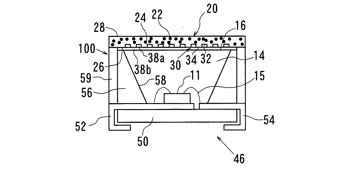
図4に示すように、第4の実施形態にかかる発光装置46は、凹部32に形成された第1の空気層38aと、樹脂成形体14と蛍光部20の第1の面16との間に形成された第2の空気層38bと、を除けば、第3の実施形態と基本的に同じ構成である。また、蛍光部20の成形体24を樹脂成形体14の外表面16と離間配置するために、本体58の周囲に側壁部58よりも高い外周壁59が形成され、外周壁の上端に成形体24の周縁部が接着されている。なお、第1の空気層38a及び第2の空気層38bに透光性材料を充填し、透光部36a,36bとしてもよい。
4). Fourth Embodiment As shown in FIG. 4, the
5.第5の実施形態
図5に示すように、第5の実施形態にかかる発光装置48は、上下に分割された樹脂成形体14a,14bの間に蛍光部20が形成されている点が第2の実施形態と同様であり、その他は、第4の実施形態と基本的に同様である。第5の実施形態にかかる発光装置48の製造方法は、基本的に第2の実施形態と同様であり、まず、LEDチップ11を樹脂成形体14aで封止し、樹脂成形体14aの平坦な表面16上に別途成形した凹凸部30を有する蛍光部20を配置させ、さらに蛍光部20の第2の面28の上に樹脂成形体14bを流し込んで封止することで製造される。
5. Fifth Embodiment As shown in FIG. 5, the
6.第6の実施形態
図6に示すように、第6の実施形態にかかる発光装置49は、筐体57の底部に配置された基板51上にモノシリックに直列接続された複数のLEDチップ11と、これら複数のLEDチップ11を封止する樹脂成形体14と、樹脂成形体14の外表面16を覆うシート状の成形体24からなる蛍光部20と、を含む。蛍光部20は、複数のLEDチップ11の光により励起されて発光する蛍光体22を含む。LEDチップ11は、基板51上に例えばn型GaN層301、p型GaN層302、p電極303、n電極304を有している。隣り合うLEDチップ11は、p電極303とn電極304とをエアブリッジ配線17で接続されている。このように複数のLEDチップをモノリシックに形成して互いに直列接続することで、各LEDチップに流れる電流は同一となり、バンドギャップエネルギーに高低が生じてもフラットな発光スペクトルが得られる。
6. Sixth Embodiment As shown in FIG. 6, a
筐体57の内部は、樹脂成形体14によって封止され、複数のLED11は樹脂成形体14中にある。蛍光部20は、第1の面26に凹部32と凸部34が交互に形成された凹凸部30を有し、第1の面26をLEDチップ11に対向して配置される。図6では発光装置49の縦断面を示しているため、凹凸部30は単純に連続する凹凸で示されているが、筐体57の開口部57aの内側全体、つまり光が放射される樹脂成形体14の外表面16に対応する領域に凹部32が網の目状の模様に形成されている。凹凸部30は、凹部32に透明材料が充填された透光部36を有している。したがって、蛍光部20は、第1の面26に形成された凸部34及び透光部36が樹脂成形体14の外表面16に密着して配置されている。凹凸部30は、凹部32または凸部34が0.05mm以上のピッチで形成されている。
The inside of the
LEDチップ11から出射された光は、樹脂成形体14を透過して、凹凸部30が形成された第1の面26から蛍光部20へ入射し、蛍光体22により吸収され、蛍光体22が励起される。蛍光体22が励起されると、その性質に応じて所定の分光スペクトル分布を有する蛍光を発光し、可視光、例えば白色光が第2の面28側から出力される。
The light emitted from the
第6の実施形態においては、第1の実施形態と同様に透光部36は凹部32を埋めるように透光性材料を充填したが、凹凸部30を全て覆うように透光部36を形成してもよいし、第2の実施形態や第4の実施形態のように空気層38を設けてもよい。なお、樹脂成形体14、蛍光部20のマトリックス材料、蛍光体22、LEDチップ11の材質は、第1の実施形態で例示したものを適宜用いることができる。
In the sixth embodiment, the
第1〜第6の実施形態においては、光源としてLEDチップ11が用いられたが、これに限らず、蛍光部によって波長変換でき、本発明の効果を奏する光源であれば、LED以外の光源、例えば電球(バルブ)、蛍光灯、冷陰極管、有機EL、無機ELなどを用いてもよい。また、光源としても用いられるLEDチップは、単数もしくは複数でもよい。第1〜第6の実施形態の凹凸部30は、凹部32が網の目状に形成されたが、凹部32または凸部34が所定のピッチで全体に形成されていれば、例えば縦縞状、横縞状であってもよい。また、凹部32または凸部34が所定のピッチの範囲内で形成されていれば、凹部32または凸部34のピッチが均等であってもランダムであってもよい。第1〜第6の実施形態の凸部34の形状は、四方を凹部32に囲まれた四角錘であるが、三角錐などの多角錘、円錐、三角柱などの多角柱、円柱でもよい。蛍光部20は、少なくともLEDチップ11からの光の放射を受ける領域に凹凸部30を設ければよく、その凹凸部30をLEDチップ11に対向させて配置すればよい。このように蛍光部20を配置することで、LEDチップ11から放射された光は、凹凸部30に入射された後、蛍光部20を透過するため、凹凸部30の効果によって高い輝度を有する発光装置となる。また、第1、第3、第6の実施形態の透光部36は、凹部32の底部を部分的に透光性材料で埋めて形成してもよいし、凸部34に至るまでの凹部32を全部埋めて形成してもよい。さらに、凸部34の上端に至るまで凸部34を含む凹凸部30を覆うようにして透光部36を形成してもよい。透光部36の表面形状は、LED10の樹脂成形体14に密着する形であってもよいし、凹凸が形成されてもよい。
In the first to sixth embodiments, the
(試料の製作)
各実施例及び比較例で用いる蛍光部として、蛍光体を含む薄い円板状の成形体を試料1〜8として製作した。
まず、試料1〜6は、表1に示すように、シリコーンゴム1gに対し、赤色蛍光体LiEu0.96Sm0.04W2O8と、緑色蛍光体ZnS:Cu,Alと、青色蛍光体(Sr,Ca,Ba)5(PO4)3Cl:Eu2+と、を適量混合した後、金型内で10MPa、130℃、5分間プレス成形して表2に示す厚さ(凸部を含む)の成形体を得た。なお、各試料における蛍光体の量が異なっているのは、各試料の相対輝度を測定するため、色度を同程度に調整したからである。また、金型内には予めNBC社製のナイロンメッシュを配置し、プレス成形でナイロンメッシュの形状を転写することで、試料1〜6の成形体の第1の面(任意の片面)に所望の凹凸部が成形されている。つまり、ナイロンメッシュの繊維部分が凹凸部の凹部になり、孔の部分が四角錘の凸部になる。成形体の隣り合う凹部のピッチ(mm)、凹部の深さ(mm)、凹部の幅(mm)及び凸部の幅(mm)は、表1に示すとおりである。また、プレス成形する際、ブラスト加工された金型を用いることで、第1の面が、算術平均粗さが0.07μmの粗面を持つ試料7(比較例1)を作成した。なお、試料8は、成形体に凹凸部がなく、第1の面26が鏡面状の比較例2である。こうして得られた成形体を直径6mmの薄い円板状に切り出し試料1〜8とした。
(Sample production)
As the fluorescent part used in each of the examples and comparative examples, thin disk-shaped molded bodies including a phosphor were manufactured as samples 1 to 8.
First, as shown in Table 1, Samples 1 to 6 have red phosphor LiEu0.96Sm0.04W 2 O 8 , green phosphor ZnS: Cu, Al, and blue phosphor (Sr, After mixing an appropriate amount of Ca, Ba) 5 (PO 4 ) 3 Cl: Eu 2+ , press molding was performed in a mold at 10 MPa at 130 ° C. for 5 minutes, and the thicknesses (including convex portions) shown in Table 2 were obtained. A molded body was obtained. Note that the amount of phosphor in each sample is different because the chromaticity is adjusted to the same level in order to measure the relative luminance of each sample. Further, a nylon mesh made by NBC Co. is placed in advance in the mold, and the shape of the nylon mesh is transferred by press molding, so that it is desired on the first surface (arbitrary one surface) of the samples 1 to 6 The uneven portion is formed. That is, the fiber portion of the nylon mesh becomes a concave portion of the concavo-convex portion, and the hole portion becomes a convex portion of the square weight. Table 1 shows the pitch (mm) of the concave portions adjacent to each other of the molded body, the depth (mm) of the concave portions, the width (mm) of the concave portions, and the width (mm) of the convex portions. Further, when press molding, a sample 7 (Comparative Example 1) having a rough surface with an arithmetic average roughness of 0.07 μm was created by using a blasted mold. Note that Sample 8 is Comparative Example 2 in which the molded body has no uneven portion and the
(輝度の測定)
次に、図7に示すように、試料1〜8の薄い円板状の成形体24をLED10の樹脂成形体14の外表面16に密着させ、第3の実施形態のような発光装置44aを作成し、発光装置44aからの全ての発光を図示されていないが積分球及び光ファイバーを介して分光光度計60に導き入れるように各装置を配置した。LED10は、樹脂成形体14の外周を金属(銅)製の筒(ステム)70で囲ったステムタイプのLEDであった。凹凸部30の凸部34は、樹脂成形体14の外表面16に密着した。なお、第3の実施形態の発光装置44aは凹部32には空気層38が形成されている。発光装置44aを発光させて分光光度計60で色度及び輝度(Cd/m2)を測定し、その結果を表2及び図9に示した。相対輝度は、試料8(比較例2)の輝度を100%とし、試料8(比較例2)の輝度に対する試料1〜7の相対輝度(%)を示した。LED10は、主発光ピーク波長395nmのepitex社製ステムタイプLED「L395−30T52(商品名)」を用いた。分光光度計60は、大塚電子社製超高感度瞬間マルチ測光システム「MCPD−7000(商品名)」を用いた。
(Measurement of brightness)
Next, as shown in FIG. 7, the thin disk-shaped molded
その結果、試料8(比較例2)の輝度に対する試料1〜6の相対輝度は、試料1〜6において100%を超えた。また、小さな粗面形状を有する試料7(比較例1)は相対輝度100%を少し上回るが、試料1〜6には及ばない。図9のように近似曲線を描いたとき、凹部32のピッチが0.16mmの試料2から相対輝度が102%を超え、、凹部32のピッチが1.30mmを超えると相対輝度が資料8に近くなることがわかった。したがって、凹部32に空気層が形成された蛍光部20は、特に凹部32のピッチが0.15mm〜1.30mmの範囲で輝度が顕著に向上することがわかった。
As a result, the relative luminance of samples 1 to 6 with respect to the luminance of sample 8 (Comparative Example 2) exceeded 100% in samples 1 to 6. Sample 7 (Comparative Example 1) having a small rough surface shape slightly exceeds the relative luminance of 100%, but does not reach Samples 1-6. When an approximate curve is drawn as shown in FIG. 9, the relative luminance exceeds 102% from the sample 2 with the pitch of the
実施例1の試料1〜6の凹凸部30及び試料7の粗面を覆うように透光性材料であるシリコーンゴムを流し込み(充填し)、脱泡後、空気が巻き込まれないように130℃、5分間加熱して凹部32を封止すると共に、凸部34の上に厚さ0.06mmの透光部36が形成された表3に示す厚さの試料1a〜7aを得た。図8に示すように、この試料1a〜7aの透光部36を実施例1と同様にLED10の樹脂成形体14の外表面16に密着させ、発光装置44を発光させて分光光度計60で色度及び輝度(Cd/m2)を測定し、その結果を表3及び図10に示した。相対輝度は、試料8(比較例2)の輝度を100%とし、試料8(比較例2)の輝度に対する試料1a〜7aの相対輝度(%)を示した。
Silicone rubber, which is a translucent material, is poured (filled) so as to cover the concavo-
その結果、試料8(比較例2)の輝度に対する試料1a〜6aの相対輝度は、100%を大きく超えた。小さな粗面形状を有する試料7aは相対輝度100%を超えたが、試料1a〜6aには明らかに及ばなかった。図10のように近似曲線を描いたとき、凹部32のピッチが0.05mm〜1.50mmの範囲で相対輝度が向上することがわかった。したがって、凹部32に透光部36が形成された試料1a〜6aは、特に凹部32のピッチが0.05mm〜1.50mmの範囲で輝度が向上し、凹部32に空気層38が形成された実施例1よりも輝度が向上することがわかった。
As a result, the relative luminance of samples 1a to 6a with respect to the luminance of sample 8 (Comparative Example 2) greatly exceeded 100%. Sample 7a having a small rough surface shape exceeded the relative luminance of 100%, but clearly did not reach samples 1a to 6a. When an approximate curve was drawn as shown in FIG. 10, it was found that the relative luminance was improved when the pitch of the
実施例3は、実施例1のRGB蛍光体の代わりにYAG蛍光体を用いて試料9〜11を得た。試料9〜11を製作する工程は、実施例2と同様であり、シリコーン樹脂10gに対してYAG蛍光体1.5gを混合して金型内でプレス成形し、さらに凹部32にシリコーンゴムを流し込み透光部を形成した。試料9〜11は、表4に示すNBC社製のナイロンメッシュを用いて凹凸部30を成形した。各試料における隣り合う凹部32のピッチ(mm)は、表4に示すとおりである。なお、試料12(比較例4)は、成形体に凹凸部がなく、第1の面26が鏡面状の比較例2と同一の形状で透光部を有さないものである。試料9〜11の透光部36を実施例1と同様にLED10の樹脂成形体14の外表面16に密着させ、発光装置44を発光させて分光光度計60で色度及び輝度(Cd/m2)を測定し、その結果を表4及び図11に示した。LED10は、主発光ピーク波長が470nmの波長を有する豊田合成社製のLEDを用いた。相対輝度は、試料12(比較例4)の輝度を100%とし、試料12(比較例4)の輝度に対する試料9〜11の相対輝度(%)を示した。
In Example 3, samples 9 to 11 were obtained using YAG phosphor instead of the RGB phosphor of Example 1. The process of manufacturing samples 9 to 11 is the same as that in Example 2. 1.5 g of YAG phosphor is mixed with 10 g of silicone resin, press-molded in the mold, and silicone rubber is poured into the
その結果、YAG蛍光体を用いた場合であっても、試料12(比較例4)の輝度に対する試料9〜11の相対輝度は100%を超えた。図11のように近似曲線を描いたとき、凹部32のピッチが0.05mm〜1.30mmの範囲で相対輝度が向上することがわかった。したがって、YAG蛍光体を用いた発光装置44において、凹部32に透光部が形成された試料9〜11は、特に凹部32のピッチが0.05mm〜1.30mmの範囲で輝度が向上することがわかった。
As a result, even when the YAG phosphor was used, the relative luminance of samples 9 to 11 with respect to the luminance of sample 12 (Comparative Example 4) exceeded 100%. When an approximate curve was drawn as shown in FIG. 11, it was found that the relative luminance was improved when the pitch of the
10 LED(発光ダイオード)
11 LEDチップ
12 ベース部材
13 ステム
14 樹脂成形体
15 ボンディングワイヤ
16 外表面
17 エアブリッジ配線
20 蛍光部
22 蛍光体
24 成形体
26 第1の面
28 第2の面
30 凹凸部
32 凹部
34 凸部
36 透光部
38 空気層
38a 第1の空気層
38b 第2の空気層
40 発光装置(第1の実施形態)
42 発光装置(第2の実施形態)
44 発光装置(第3の実施形態)
46 発光装置(第4の実施形態)
48 発光装置(第5の実施形態)
49 発光装置(第6の実施形態)
50 セラミック基板
51 基板
52 配線導体(アノードリード)
54 配線導体(カソードリード)
56 本体
57 筐体
57a 開口部
58 側壁部
60 分光光度計
100 SMD型LED
301 n型GaN層
302 p型GaN層
303 p電極
304 n電極
10 LED (light emitting diode)
11
42 Light Emitting Device (Second Embodiment)
44 Light Emitting Device (Third Embodiment)
46 Light Emitting Device (Fourth Embodiment)
48 Light Emitting Device (Fifth Embodiment)
49 Light Emitting Device (Sixth Embodiment)
50
54 Wiring conductor (cathode lead)
56
301 n-type GaN layer 302 p-type GaN layer 303 p-electrode 304 n-electrode
Claims (3)
前記蛍光部は、前記光源側の面に凹部と凸部が交互に形成された凹凸部を有し、かつ、前記樹脂成形体に積層して配置され、
前記凹凸部は、前記凹部に空気層を有し、かつ、前記凹部が前記樹脂成形体に非接触状態であり、
前記凹部は、ピッチが0.15mm〜1.30mm、深さが0.003mm〜0.510mm、幅が0.04mm〜0.35mmで形成された発光装置。 A light source composed of an LED chip, a resin molded body that seals the LED chip , and a fluorescent portion that is formed of a polymer material including a phosphor that is excited by the light of the light source to emit light,
The fluorescent portion has a concave and convex portion in which concave portions and convex portions are alternately formed on the surface on the light source side, and is laminated and disposed on the resin molded body,
The concavo-convex portion has an air layer in the concave portion, and the concave portion is in a non-contact state with the resin molded body,
The concave portion is a light emitting device having a pitch of 0.15 mm to 1.30 mm, a depth of 0.003 mm to 0.510 mm, and a width of 0.04 mm to 0.35 mm .
前記LEDチップは、350nm〜500nmの範囲に主発光ピーク波長を有する発光装置。 In claim 1 ,
The LED chip is a light emitting device having a main emission peak wavelength in a range of 350 nm to 500 nm.
前記蛍光部の面に凹部と凸部が交互に形成された凹凸部を形成する工程と、
前記面を前記光源に対向して配置する工程と、
を有し、
前記面を配置する工程は、前記凹部に空気層が形成されるように、前記凹部を前記樹脂成形体に非接触状態で前記蛍光部と前記樹脂成形体とを積層し、
前記凹凸部を形成する工程は、前記凹部のピッチが0.15mm〜1.30mm、前記凹部の深さが0.003mm〜0.510mm、前記凹部の幅が0.04mm〜0.35mmとなるように形成した発光装置の製造方法。 Manufacture of a light-emitting device having a light source composed of an LED chip, a resin molded body that seals the LED chip , and a fluorescent part that is formed of a polymer material including a phosphor that is excited by the light of the light source to emit light In the method
Forming a concavo- convex portion in which concave portions and convex portions are alternately formed on the surface of the fluorescent portion;
Arranging the surface to face the light source;
Have
The step of disposing the surface includes laminating the fluorescent portion and the resin molded body in a non-contact state with the concave portion so that an air layer is formed in the concave portion,
In the step of forming the concave and convex portions, the pitch of the concave portions is 0.15 mm to 1.30 mm, the depth of the concave portions is 0.003 mm to 0.510 mm, and the width of the concave portions is 0.04 mm to 0.35 mm. A method for manufacturing a light emitting device formed as described above.
Priority Applications (1)
| Application Number | Priority Date | Filing Date | Title |
|---|---|---|---|
| JP2006181800A JP4868960B2 (en) | 2006-06-30 | 2006-06-30 | Light emitting device and manufacturing method thereof |
Applications Claiming Priority (1)
| Application Number | Priority Date | Filing Date | Title |
|---|---|---|---|
| JP2006181800A JP4868960B2 (en) | 2006-06-30 | 2006-06-30 | Light emitting device and manufacturing method thereof |
Related Child Applications (1)
| Application Number | Title | Priority Date | Filing Date |
|---|---|---|---|
| JP2011184491A Division JP5291162B2 (en) | 2011-08-26 | 2011-08-26 | Light emitting device and manufacturing method thereof |
Publications (2)
| Publication Number | Publication Date |
|---|---|
| JP2008010748A JP2008010748A (en) | 2008-01-17 |
| JP4868960B2 true JP4868960B2 (en) | 2012-02-01 |
Family
ID=39068672
Family Applications (1)
| Application Number | Title | Priority Date | Filing Date |
|---|---|---|---|
| JP2006181800A Expired - Fee Related JP4868960B2 (en) | 2006-06-30 | 2006-06-30 | Light emitting device and manufacturing method thereof |
Country Status (1)
| Country | Link |
|---|---|
| JP (1) | JP4868960B2 (en) |
Cited By (1)
| Publication number | Priority date | Publication date | Assignee | Title |
|---|---|---|---|---|
| JP2011233942A (en) * | 2011-08-26 | 2011-11-17 | Fine Rubber Kenkyusho:Kk | Light-emitting device and manufacturing method thereof |
Families Citing this family (3)
| Publication number | Priority date | Publication date | Assignee | Title |
|---|---|---|---|---|
| JP2010258093A (en) * | 2009-04-22 | 2010-11-11 | Ccs Inc | Light emitting device |
| JP2014038876A (en) * | 2010-12-15 | 2014-02-27 | Panasonic Corp | Semiconductor light-emitting device |
| CN107123724B (en) * | 2017-03-29 | 2023-05-23 | 华南理工大学 | Method and device for molding electric control variable curved surface fluorescent membrane |
Family Cites Families (4)
| Publication number | Priority date | Publication date | Assignee | Title |
|---|---|---|---|---|
| JP3434658B2 (en) * | 1997-01-14 | 2003-08-11 | サンケン電気株式会社 | Semiconductor light emitting device |
| JP2004235337A (en) * | 2003-01-29 | 2004-08-19 | Toyoda Gosei Co Ltd | Light emitting diode |
| US20050156510A1 (en) * | 2004-01-21 | 2005-07-21 | Chua Janet B.Y. | Device and method for emitting output light using group IIB element selenide-based and group IIA element gallium sulfide-based phosphor materials |
| JP2005327841A (en) * | 2004-05-13 | 2005-11-24 | Asahi Rubber:Kk | Cap for light emitting diode, and light emitting diode device |
-
2006
- 2006-06-30 JP JP2006181800A patent/JP4868960B2/en not_active Expired - Fee Related
Cited By (1)
| Publication number | Priority date | Publication date | Assignee | Title |
|---|---|---|---|---|
| JP2011233942A (en) * | 2011-08-26 | 2011-11-17 | Fine Rubber Kenkyusho:Kk | Light-emitting device and manufacturing method thereof |
Also Published As
| Publication number | Publication date |
|---|---|
| JP2008010748A (en) | 2008-01-17 |
Similar Documents
| Publication | Publication Date | Title |
|---|---|---|
| KR101008762B1 (en) | Light-emitting device and method for manufacturing the same | |
| US7718991B2 (en) | Lighting device and method of making | |
| US9420642B2 (en) | Light emitting apparatus and lighting apparatus | |
| KR100944008B1 (en) | White light emitting diode and fabrication method thereof | |
| JP3898721B2 (en) | Light emitting device and lighting device | |
| KR102277127B1 (en) | Light emitting device package | |
| US8421102B2 (en) | Semiconductor light-emitting device having a member in a periphery made of a material whose color, transparency or adhesiveness changes overtime due to light or heat emission from the emitting element | |
| WO2009156856A2 (en) | Led with improved external light extraction efficiency | |
| JP2006237264A (en) | Light emitting device and lighting apparatus | |
| KR20110019394A (en) | A light emitting device having a transparent thermally conductive layer | |
| JP2011507287A (en) | Lighting equipment | |
| JP2008053702A (en) | Light-emitting device, and lighting device | |
| KR20160036489A (en) | Light emitting device | |
| JP2008010749A (en) | Light-emitting apparatus and manufacturing method thereof | |
| JP2014060328A (en) | Light-emitting device | |
| KR101575366B1 (en) | Light emitting device package | |
| US20140376223A1 (en) | Light source with led chip and luminophore layer | |
| JP2006295230A (en) | Light emitting device and lighting apparatus | |
| JP4868960B2 (en) | Light emitting device and manufacturing method thereof | |
| JP2013038353A (en) | Light-emitting module | |
| US9989197B2 (en) | Optical device and light source module including the same | |
| JP2009099759A (en) | Light emitting device | |
| US10964859B2 (en) | Light-emitting device and method of manufacturing the same | |
| JP4417757B2 (en) | LIGHT EMITTING DEVICE, ITS MANUFACTURING METHOD, AND LIGHTING DEVICE | |
| KR20180093989A (en) | LED device adopting color tuning filtering using multiple neodymium and fluorine compounds |
Legal Events
| Date | Code | Title | Description |
|---|---|---|---|
| A621 | Written request for application examination |
Free format text: JAPANESE INTERMEDIATE CODE: A621 Effective date: 20090430 |
|
| A521 | Written amendment |
Free format text: JAPANESE INTERMEDIATE CODE: A523 Effective date: 20100212 |
|
| A131 | Notification of reasons for refusal |
Free format text: JAPANESE INTERMEDIATE CODE: A131 Effective date: 20110629 |
|
| A977 | Report on retrieval |
Free format text: JAPANESE INTERMEDIATE CODE: A971007 Effective date: 20110629 |
|
| A521 | Written amendment |
Free format text: JAPANESE INTERMEDIATE CODE: A523 Effective date: 20110826 |
|
| TRDD | Decision of grant or rejection written | ||
| A01 | Written decision to grant a patent or to grant a registration (utility model) |
Free format text: JAPANESE INTERMEDIATE CODE: A01 Effective date: 20111026 |
|
| A01 | Written decision to grant a patent or to grant a registration (utility model) |
Free format text: JAPANESE INTERMEDIATE CODE: A01 |
|
| A61 | First payment of annual fees (during grant procedure) |
Free format text: JAPANESE INTERMEDIATE CODE: A61 Effective date: 20111115 |
|
| R150 | Certificate of patent or registration of utility model |
Free format text: JAPANESE INTERMEDIATE CODE: R150 |
|
| FPAY | Renewal fee payment (event date is renewal date of database) |
Free format text: PAYMENT UNTIL: 20141125 Year of fee payment: 3 |
|
| R250 | Receipt of annual fees |
Free format text: JAPANESE INTERMEDIATE CODE: R250 |
|
| R250 | Receipt of annual fees |
Free format text: JAPANESE INTERMEDIATE CODE: R250 |
|
| LAPS | Cancellation because of no payment of annual fees |