JP2014060328A - Light-emitting device - Google Patents
Light-emitting device Download PDFInfo
- Publication number
- JP2014060328A JP2014060328A JP2012205653A JP2012205653A JP2014060328A JP 2014060328 A JP2014060328 A JP 2014060328A JP 2012205653 A JP2012205653 A JP 2012205653A JP 2012205653 A JP2012205653 A JP 2012205653A JP 2014060328 A JP2014060328 A JP 2014060328A
- Authority
- JP
- Japan
- Prior art keywords
- light
- phosphor
- light emitting
- resin layer
- emitting element
- Prior art date
- Legal status (The legal status is an assumption and is not a legal conclusion. Google has not performed a legal analysis and makes no representation as to the accuracy of the status listed.)
- Pending
Links
- OAICVXFJPJFONN-UHFFFAOYSA-N Phosphorus Chemical compound [P] OAICVXFJPJFONN-UHFFFAOYSA-N 0.000 claims abstract description 188
- 229920005989 resin Polymers 0.000 claims abstract description 185
- 239000011347 resin Substances 0.000 claims abstract description 185
- 229910052782 aluminium Inorganic materials 0.000 claims description 9
- 229910004283 SiO 4 Inorganic materials 0.000 claims description 6
- 229910017639 MgSi Inorganic materials 0.000 claims description 4
- 239000000203 mixture Substances 0.000 claims description 4
- 102100032047 Alsin Human genes 0.000 claims description 3
- 101710187109 Alsin Proteins 0.000 claims description 3
- 229910016066 BaSi Inorganic materials 0.000 claims description 3
- 229910052693 Europium Inorganic materials 0.000 claims description 3
- 229910003668 SrAl Inorganic materials 0.000 claims description 3
- 229910052771 Terbium Inorganic materials 0.000 claims description 3
- 229910052727 yttrium Inorganic materials 0.000 claims description 3
- 229910052733 gallium Inorganic materials 0.000 claims description 2
- 238000009877 rendering Methods 0.000 abstract description 9
- 239000000126 substance Substances 0.000 description 16
- 239000000758 substrate Substances 0.000 description 11
- 230000004048 modification Effects 0.000 description 9
- 238000012986 modification Methods 0.000 description 9
- 230000007423 decrease Effects 0.000 description 7
- 230000000694 effects Effects 0.000 description 7
- 239000000463 material Substances 0.000 description 7
- 239000007787 solid Substances 0.000 description 6
- 230000020169 heat generation Effects 0.000 description 5
- 238000006243 chemical reaction Methods 0.000 description 4
- 239000003822 epoxy resin Substances 0.000 description 4
- LNEPOXFFQSENCJ-UHFFFAOYSA-N haloperidol Chemical compound C1CC(O)(C=2C=CC(Cl)=CC=2)CCN1CCCC(=O)C1=CC=C(F)C=C1 LNEPOXFFQSENCJ-UHFFFAOYSA-N 0.000 description 4
- 229920000647 polyepoxide Polymers 0.000 description 4
- 229920002050 silicone resin Polymers 0.000 description 4
- -1 (Sr Chemical compound 0.000 description 3
- 230000005540 biological transmission Effects 0.000 description 3
- 239000000919 ceramic Substances 0.000 description 3
- 239000003795 chemical substances by application Substances 0.000 description 3
- 239000000945 filler Substances 0.000 description 3
- 229910052751 metal Inorganic materials 0.000 description 3
- 239000002184 metal Substances 0.000 description 3
- 238000000034 method Methods 0.000 description 3
- 239000004065 semiconductor Substances 0.000 description 3
- 238000001228 spectrum Methods 0.000 description 3
- BQCADISMDOOEFD-UHFFFAOYSA-N Silver Chemical compound [Ag] BQCADISMDOOEFD-UHFFFAOYSA-N 0.000 description 2
- 239000003086 colorant Substances 0.000 description 2
- 238000009792 diffusion process Methods 0.000 description 2
- 238000004519 manufacturing process Methods 0.000 description 2
- 150000004767 nitrides Chemical class 0.000 description 2
- 238000007747 plating Methods 0.000 description 2
- 229920001707 polybutylene terephthalate Polymers 0.000 description 2
- 238000007789 sealing Methods 0.000 description 2
- 229910052709 silver Inorganic materials 0.000 description 2
- 239000004332 silver Substances 0.000 description 2
- 108010043121 Green Fluorescent Proteins Proteins 0.000 description 1
- 229910052765 Lutetium Inorganic materials 0.000 description 1
- 239000004677 Nylon Substances 0.000 description 1
- 206010037660 Pyrexia Diseases 0.000 description 1
- 229910004298 SiO 2 Inorganic materials 0.000 description 1
- 229910010413 TiO 2 Inorganic materials 0.000 description 1
- 238000000862 absorption spectrum Methods 0.000 description 1
- XAGFODPZIPBFFR-UHFFFAOYSA-N aluminium Chemical compound [Al] XAGFODPZIPBFFR-UHFFFAOYSA-N 0.000 description 1
- GTDCAOYDHVNFCP-UHFFFAOYSA-N chloro(trihydroxy)silane Chemical compound O[Si](O)(O)Cl GTDCAOYDHVNFCP-UHFFFAOYSA-N 0.000 description 1
- 239000004020 conductor Substances 0.000 description 1
- 238000000295 emission spectrum Methods 0.000 description 1
- 238000000605 extraction Methods 0.000 description 1
- 239000002223 garnet Substances 0.000 description 1
- 239000011521 glass Substances 0.000 description 1
- 229920006015 heat resistant resin Polymers 0.000 description 1
- 229920001778 nylon Polymers 0.000 description 1
- 229920000515 polycarbonate Polymers 0.000 description 1
- 239000004417 polycarbonate Substances 0.000 description 1
- 229910052706 scandium Inorganic materials 0.000 description 1
- 150000004760 silicates Chemical class 0.000 description 1
- 239000012780 transparent material Substances 0.000 description 1
- VWQVUPCCIRVNHF-UHFFFAOYSA-N yttrium atom Chemical compound [Y] VWQVUPCCIRVNHF-UHFFFAOYSA-N 0.000 description 1
Images


Abstract
Description
本発明は、発光装置に関し、特に、発光素子と蛍光体とを含む発光装置に関する。 The present invention relates to a light emitting device, and more particularly to a light emitting device including a light emitting element and a phosphor.
一般に、発光ダイオード(LED:Light Emitting Diode)、レーザーダイオード(LD:Laser Diode)等の発光素子を用いた発光装置は、小型で電力効率がよく、鮮やかな色を発光することで知られている。この発光装置に用いられる発光素子は、球切れ等の心配が少なく、また振動やオン・オフ点灯の繰り返しに対して高い耐久性を有するため、発光装置の寿命が長いという特徴がある。さらに、これに加えて初期駆動特性に優れるという特徴を有する。このような優れた特性を有するため、発光素子を用いる発光装置は、LED電球やLED蛍光灯、シーリングライトのような照明器具、ディスプレイ等の各種の光源として広く利用されている。 2. Description of the Related Art Generally, light emitting devices using light emitting elements such as light emitting diodes (LEDs) and laser diodes (LDs) are known to be small, power efficient, and emit bright colors. . The light-emitting element used in this light-emitting device has a feature that the life of the light-emitting device is long because there is little fear of a ball breakage and high durability against repeated vibration and on / off lighting. Further, in addition to this, it has a feature of excellent initial drive characteristics. Because of such excellent characteristics, light-emitting devices using light-emitting elements are widely used as various light sources such as LED bulbs, LED fluorescent lamps, lighting fixtures such as ceiling lights, and displays.
これらの発光素子の発する光のスペクトルは、一般的に、狭い波長範囲にピークを有している。これに対して、照明器具等に用いる発光装置の発する光には、高い演色性が求められることが多く、例えば白色光のように相対的に広いスペクトルを有することが求められている。
このため、このような用途において、発光素子を用いた多くの発光装置は、例えば赤色蛍光体と青緑〜緑色蛍光体または黄緑〜黄色蛍光体とのような2種類以上の蛍光体が混合した状態で含まれている蛍光体含有層を有している。そして、これらの蛍光体は発光素子からの光を吸収し異なる波長(異なる色)に変換した光を発する。この結果、発光素子から発光され蛍光体に吸収されずに蛍光体含有層を通過した光と、第1の蛍光体(例えば、赤色蛍光体)により変換されて蛍光体含有層から出た光と、第2の蛍光体(第1の蛍光体と異なる種類の蛍光体、例えば、青緑〜緑色蛍光体または黄緑〜黄色蛍光体)により変換された光(第1の蛍光体により変換された光と異なる波長を有する)光とが混合されることで広いスペクトルの光を得ている。
The spectrum of light emitted from these light emitting elements generally has a peak in a narrow wavelength range. On the other hand, light emitted from a light emitting device used for a lighting fixture or the like is often required to have high color rendering properties, and is required to have a relatively broad spectrum, such as white light.
For this reason, in such applications, many light-emitting devices using light-emitting elements are a mixture of two or more types of phosphors such as a red phosphor and a blue-green to green phosphor or a yellow-green to yellow phosphor. The phosphor-containing layer is included in the state. These phosphors absorb light from the light emitting element and emit light converted to different wavelengths (different colors). As a result, light emitted from the light-emitting element and passed through the phosphor-containing layer without being absorbed by the phosphor, and light emitted from the phosphor-containing layer after being converted by the first phosphor (for example, red phosphor) , Light converted by the second phosphor (a different type of phosphor from the first phosphor, for example, blue-green to green phosphor or yellow-green to yellow phosphor) (converted by the first phosphor) Light of a wide spectrum is obtained by mixing light having a wavelength different from that of light.
一般的には、樹脂中に2種類以上の蛍光体を含有させ、この蛍光体を含む樹脂を発光素子の周りに配置した後、硬化させることにより、発光素子と接触した蛍光体含有層を形成した、砲弾型または表面実装型の発光装置が多く用いられている。 Generally, two or more kinds of phosphors are contained in a resin, and a phosphor-containing layer in contact with the light emitting element is formed by placing a resin containing the phosphor around the light emitting element and then curing the resin. In addition, a bullet-type or surface-mount type light emitting device is often used.
しかし、蛍光体は、その種類によっては、長時間高い温度で保持されるとその特性が悪化する場合がある。すなわち、蛍光体含有層と発光素子とが接触しているモールド型の発光素子では、発光素子の発熱により蛍光体の温度が上昇し発光効率が低下する場合がある。
また、2種類の蛍光体が混合された状態で含まれている蛍光体含有層を用いる従来の発光装置では2種の蛍光体のうち、発光(変換された光)が長波長側の蛍光体の吸収スペクトルが、発光が短波長側である蛍光体の発光スペクトルと重なるため、短波長側の発光が長波長側の蛍光体に吸収され、発光効率および演色性が低下するという問題がある。
However, depending on the type of phosphor, its characteristics may deteriorate when held at a high temperature for a long time. That is, in a mold-type light emitting element in which the phosphor-containing layer and the light emitting element are in contact, the temperature of the phosphor may increase due to heat generation of the light emitting element, and the light emission efficiency may decrease.
Moreover, in the conventional light-emitting device using the phosphor-containing layer that is included in a state where two types of phosphors are mixed, among the two types of phosphors, the phosphor that emits light (converted light) has a long wavelength side. The absorption spectrum overlaps with the emission spectrum of the phosphor having a short wavelength side, so that the short wavelength side light is absorbed by the long wavelength side phosphor and the light emission efficiency and the color rendering are lowered.
そこで、このような問題を回避するために、例えば特許文献1に示されるように、発光素子から離間させて配置した透過窓(フィルム)の内側(発光素子に近い側)に赤色蛍光体層(発光物質層)を形成し、透過窓の外側に黄緑〜黄色蛍光体層を形成した発光装置が知られている。
Therefore, in order to avoid such a problem, for example, as shown in Patent Document 1, a red phosphor layer (on the side close to the light emitting element) (on the side close to the light emitting element) inside the transmission window (film) arranged away from the
しかし、特許文献1の発光装置では、発光素子から出た光が、赤色蛍光体層と透過窓と黄緑〜黄色蛍光体層とから成る3層構造(3の固体層)を通過する必要がある。そして、それぞれの固体層を通過さする際には、各固体層に入ろうとする光の一部は、表面で反射してしまう。このように反射される光は、通過する固体層の数が増加するほど多くなり、発光装置として取り出せる光が低下するため、効率が低下してしまうという問題がある。 However, in the light emitting device of Patent Document 1, it is necessary for light emitted from the light emitting element to pass through a three-layer structure (three solid layers) including a red phosphor layer, a transmission window, and a yellow-green to yellow phosphor layer. is there. When passing through each solid layer, a part of the light entering the respective solid layer is reflected on the surface. The amount of light reflected in this way increases as the number of solid layers that pass through increases, and the light that can be extracted as a light-emitting device decreases.
本願発明は、このような要求に応えるものである。すなわち、本願発明は、高い発光効率を有し、発する光が優れた演色性を有するとともに、使用する赤色蛍光体の量を抑制した発光装置を提供することを目的とする。 The present invention meets these requirements. That is, an object of the present invention is to provide a light-emitting device having high luminous efficiency, excellent color rendering properties of emitted light, and a reduced amount of red phosphor to be used.
本願発明に係る第1の態様は、発光素子と、前記発光素子と接触しかつ前記発光素子のを覆うように配置された、赤色蛍光体を含む第1の樹脂層と、前記第1の樹脂層の外側に該第1の樹脂層から離間して配置された、前記赤色蛍光体よりも発光ピーク波長の短い蛍光体を含む第2の樹脂層と、を有することを特徴とする発光装置である。 According to a first aspect of the present invention, there is provided a light-emitting element, a first resin layer including a red phosphor disposed in contact with the light-emitting element and covering the light-emitting element, and the first resin. And a second resin layer including a phosphor having an emission peak wavelength shorter than that of the red phosphor, which is disposed outside the layer and spaced apart from the first resin layer. is there.
本願発明に係る第2の態様は、前記第1の樹脂層と前記第2の樹脂層の間に空気層が形成されていることを特徴とする態様1に記載の発光装置である。 A second aspect according to the present invention is the light emitting device according to aspect 1, wherein an air layer is formed between the first resin layer and the second resin layer.
本願発明に係る第3の態様は、前記第1の樹脂層と前記第2の樹脂層の間に、実質的に蛍光体を含まない樹脂層が形成されていることを特徴とする態様1に記載の発光装置である。 According to a third aspect of the present invention, in the first aspect, a resin layer that does not substantially contain a phosphor is formed between the first resin layer and the second resin layer. It is a light-emitting device of description.
本願発明に係る第4の態様は、前記発光素子が発する光のピーク波長が420nm〜490nmであることを特徴とする態様1〜3のいずれかに記載の発光装置である。 A fourth aspect according to the present invention is the light emitting device according to any one of aspects 1 to 3, wherein a peak wavelength of light emitted from the light emitting element is 420 nm to 490 nm.
本願発明の第5に係る態様は、前記赤色蛍光体よりも発光ピーク波長の短い蛍光体が、青緑〜緑色蛍光体を含み、該青緑〜緑色蛍光体が、Ca8MgSi4O16Cl2:Eu、(Si,Al)6(N,O)8:Eu、BaSi2O2N2:Eu、(Ba,Sr)2SiO4:Eu、Sr4Al14O25:Eu、SrAl2O4:Eu、SrGa2S4:EuおよびBa3Si6N2O12:Euから成る群から選択される少なくとも1つを含むことを特徴とする態様1〜4のいずれかに記載の発光装置である。
In a fifth aspect of the present invention, the phosphor having an emission peak wavelength shorter than that of the red phosphor includes a blue-green to green phosphor, and the blue-green to green phosphor is Ca 8 MgSi 4 O 16 C. l2: Eu, (Si, Al ) 6 (N, O) 8: Eu, BaSi 2 O 2 N 2: Eu, (Ba, Sr) 2 SiO 4: Eu, Sr 4 Al 14 O 25: Eu,
本願発明の第6に係る態様は、前記赤色蛍光体よりも発光ピーク波長の短い蛍光体が、黄緑〜黄色蛍光体を含み、該黄緑〜黄色蛍光体が、(Y,Lu,Gd,Tb)3(Al,Ga)5O12:Ce、(Sr,Ba)2SiO4:Eu、(Ca,Sr)Si2O2N2:Eu、La3Si6N11:Ce、Ca3Sc2Si3O12:Ce、CaSc2O4:Ce、(Sr,Ca,Ba)Ga2S4:EuおよびZnS:Cuから成る群から選択される少なくとも1つを含むことを特徴とする態様1〜5のいずれかに記載の発光装置である。 In a sixth aspect of the present invention, the phosphor having an emission peak wavelength shorter than that of the red phosphor includes a yellowish green to yellow phosphor, and the yellowish green to yellow phosphor is (Y, Lu, Gd, Tb) 3 (Al, Ga) 5 O 12 : Ce, (Sr, Ba) 2 SiO 4 : Eu, (Ca, Sr) Si 2 O 2 N 2 : Eu, La 3 Si 6 N 11 : Ce, Ca 3 It includes at least one selected from the group consisting of Sc 2 Si 3 O 12 : Ce, CaSc 2 O 4 : Ce, (Sr, Ca, Ba) Ga 2 S 4 : Eu and ZnS: Cu. It is a light-emitting device in any one of aspect 1-5.
本願発明の第7に係る態様は、前記赤色蛍光体が、(Ca,Sr)AlSiN3:Eu、(Ca,Sr)2Si5N8:Eu、CaSiN2:Eu、(Ca,Sr)S:Eu、K2SiF6:Mn、LiEuW2O8およびCaX(Si,Al)12(N,O)16:Euから成る群から選択される少なくとも1つを含むことを特徴とする態様1〜6のいずれかに記載の発光装置である。 According to a seventh aspect of the present invention, in the red phosphor, the (Ca, Sr) AlSiN 3 : Eu, (Ca, Sr) 2 Si 5 N 8 : Eu, CaSiN 2 : Eu, (Ca, Sr) S And at least one selected from the group consisting of: Eu, K 2 SiF 6 : Mn, LiEuW 2 O 8 and Ca X (Si, Al) 12 (N, O) 16 : Eu It is a light-emitting device in any one of -6.
本願発明に係る発光装置は、耐熱性に優れ、熱による発光効率の低下が起こりにくい赤色蛍光体を含む第1の樹脂層を発光素子と接触して発光素子を覆うように配置している。
一方、熱の影響を受けやすく、温度が上昇すると発光効率が低下しやすい、赤色蛍光体よりも発光ピーク波長の短い蛍光体を含む第2の樹脂層を第1の樹脂層の外側(発光素子から遠ざかる方向)に第1の樹脂層から離間して配置している。このため、第2の樹脂層に含まれる蛍光体(赤色蛍光体より発光波長の短い蛍光体)は発光素子の発熱の影響をほとんど受けず、発光効率の低下を抑制できる。また、発光素子から出射した光は、第1の樹脂層と第2の樹脂層の2つの固体層を通過するだけでよい。このため、本願発明に係る発光装置は、高い発光効率および高い演色性を得ることができる。
In the light-emitting device according to the present invention, the first resin layer containing a red phosphor that has excellent heat resistance and is unlikely to cause a decrease in light emission efficiency due to heat is disposed so as to contact the light-emitting element and cover the light-emitting element.
On the other hand, the second resin layer containing a phosphor having a shorter emission peak wavelength than the red phosphor, which is easily affected by heat and whose emission efficiency is likely to decrease as the temperature rises, is disposed outside the first resin layer (light emitting element). In a direction away from the first resin layer). For this reason, the phosphor contained in the second resin layer (a phosphor having a shorter emission wavelength than that of the red phosphor) is hardly affected by the heat generated by the light emitting element, and the decrease in the light emission efficiency can be suppressed. The light emitted from the light emitting element only needs to pass through the two solid layers of the first resin layer and the second resin layer. For this reason, the light-emitting device which concerns on this invention can obtain high luminous efficiency and high color rendering property.
この結果、本願発明は、高い効率を有し、発する光が優れた演色性を有するとともに、使用する赤色蛍光体の量を抑制した発光装置を提供することができる。 As a result, the present invention can provide a light-emitting device that has high efficiency, emits light with excellent color rendering, and suppresses the amount of red phosphor used.
以下、図面に基づいて本発明の実施形態を詳細に説明する。なお、以下の説明では、必要に応じて特定の方向や位置を示す用語(例えば、「上」、「下」、「右」、「左」及びそれらの用語を含む別の用語)を用いるが、それらの用語の使用は図面を参照した発明の理解を容易にするためであって、それらの用語の意味によって本発明の技術的範囲が制限されるものではない。また、複数の図面に表れる同一符号の部分は同一または対応する部分もしくは部材を示す。 Hereinafter, embodiments of the present invention will be described in detail with reference to the drawings. In the following description, terms indicating a specific direction and position (for example, “up”, “down”, “right”, “left” and other terms including those terms) are used as necessary. These terms are used for easy understanding of the invention with reference to the drawings, and the technical scope of the present invention is not limited by the meaning of these terms. Moreover, the part of the same code | symbol appearing in several drawing shows the same or corresponding part or member.
本願発明者らは、耐熱性に優れ、発光素子の発熱により加熱されても発光効率の低下が少ない赤色蛍光体の特性と、温度特性が悪く、温度が高くなると発光効率が低下しやすい、赤色蛍光体よりも発光ピーク波長の短い蛍光体(例えば青緑〜緑色蛍光体および黄緑〜黄色蛍光体)の特性を考慮することにより本願発明の発光装置に至ったものである。 The inventors of the present application have excellent heat resistance, and the characteristics of the red phosphor and the temperature characteristics are poor even when heated by the heat generated by the light-emitting element, and the temperature characteristics are poor. The light emitting device of the present invention has been achieved by considering the characteristics of phosphors having a shorter emission peak wavelength than phosphors (for example, blue-green to green phosphors and yellow-green to yellow phosphors).
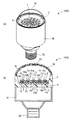
図1は、本願発明に係る発光装置100の断面図である。
発光装置100は、発光素子12と、赤色蛍光体である第1の蛍光体10を含む第1の樹脂層8と、発光ピーク波長が赤色蛍光体のピーク波長よりも短い第2の蛍光体20を含む第2の樹脂層18とを含む。
FIG. 1 is a cross-sectional view of a
The
第1の樹脂層8は、発光素子12と接触し、発光素子12を覆うように配置されている。これにより、赤色蛍光体(第1の蛍光体)10を発光素子12の近傍(例えば、発光素子12の表面から10mm以内の領域)に配置できる。
このように、赤色蛍光体を発光素子12の近傍に配置することにより、発光素子12からの光が広く拡散する前に、その一部を赤色蛍光体10に吸収させることができる。
また、上述したように、赤色蛍光体10は、温度特性に優れ、温度が上昇してもほとんど発光効率が低下しない。従って、発光素子12の発熱により赤色蛍光体10の温度が上昇しても問題ない。
The
As described above, by arranging the red phosphor in the vicinity of the
Further, as described above, the
第2の樹脂層18は、第1の樹脂層8の外側(発光素子12から遠ざかる方向)に第1の樹脂層8から離間して配置されている。これにより赤色蛍光体(第1の蛍光体)10よりも発光ピーク波長が短い第2の蛍光体20が、赤色蛍光体10の外側(赤色蛍光体10よりも発光素子12から離れた位置)に赤色蛍光体10から離間して配置されている。
The
第2の樹脂層18が第1の樹脂層8の外側に第1の樹脂層8から離間して配置されていることにより、発光素子12の発熱により第2の樹脂層18の内部に分散した第2の蛍光体20の温度が上昇するのを抑制できる。この結果、第2の蛍光体20が加熱され発光効率が低下するのを確実に抑制できる。
By disposing the
また、第2の蛍光体20を赤色蛍光体10の外側に赤色蛍光体10から離間して配置することにより、第2の蛍光体20が発光する、例えば、緑色光または黄色光のような、赤色蛍光体が発光する光りよりも波長の短い光が、赤色蛍光体10に吸収されるのを抑制することができる。このため、発光装置100が発する光は高い演色性を有している。
Further, by arranging the
さらに、発光素子8が発する光(この場合は、蛍光体により波長変換された光を含む)は、第1の樹脂層8と第2の樹脂層18との2つの固体層を通過するだけで発光装置100の外側に達するため、発光装置100は、高い発光効率を得ることができる。
Furthermore, the light emitted from the light emitting element 8 (in this case, including light that has been wavelength-converted by the phosphor) only passes through the two solid layers of the
また、発光装置100は、上述のように、第1の樹脂層8が、発光素子12と接触し、発光素子12を覆うように配置されていることから、赤色蛍光体10を発光素子12の近傍に配置することとなり、発光素子12からの光が広く拡散する前に、その一部を赤色蛍光体10に吸収させることができる。
従って、例えば特許文献1が開示する発光装置のような、赤色蛍光体を発光素子から離れて配置した発光装置と比べて、所望の強さの赤色光を発光させるのに使用する赤色蛍光体の量を少なくすることができるという効果も有する。
赤色蛍光体は、例えば青緑〜緑色蛍光体および黄緑〜黄色蛍光体のような、赤色蛍光体よりも発光ピーク波長の短い蛍光体と比べて高価であることが多い。このため、赤色蛍光体の使用量を低減できることは、発光装置全体の製造コストの低減に大きく寄与する。
Further, as described above, the
Therefore, for example, the red phosphor used to emit red light having a desired intensity as compared with a light emitting device in which the red phosphor is arranged away from the light emitting element, such as the light emitting device disclosed in Patent Document 1. There is also an effect that the amount can be reduced.
Red phosphors are often more expensive than phosphors having a shorter emission peak wavelength than red phosphors, such as blue-green to green phosphors and yellow-green to yellow phosphors. For this reason, being able to reduce the usage-amount of red fluorescent substance contributes greatly to reduction of the manufacturing cost of the whole light-emitting device.
さらに、発光装置100は、以下に示す理由から色むら改善の効果も有する。
例えば特許文献1が開示する発光装置のように、発光素子と全ての蛍光体層とが離間して配置されていると色むらの生じやすい傾向がある。発光素子は、通常、上面と側面のように角度によって出射される光の量は異なっている。よって、蛍光体層に入射する発光素子からの光の量は、例えば上面視(図1の上から下方向に観る)した場合において発光素子の直上とその周辺とでは異なる。そして、一般的に、発光素子から入射する光量が少ないほど蛍光体により波長変換させる割合が多くなり、波長変換されずに蛍光体層を通り抜ける光の割合が少なくなる。
このため、発光素子からの光(波長変換されていない光)と蛍光体により波長変換された光との比率が、蛍光体層表面の場所によって異なってしまい、最終的には発光装置の色ムラとして現れる場合がある。
Furthermore, the
For example, as in the light-emitting device disclosed in Patent Document 1, when the light-emitting elements and all the phosphor layers are arranged apart from each other, uneven color tends to occur. The amount of light emitted from the light emitting element is usually different depending on the angle such as the upper surface and the side surface. Therefore, the amount of light from the light emitting element incident on the phosphor layer is different between, for example, directly above the light emitting element and its periphery in a top view (viewed from the top to the bottom in FIG. 1). In general, the smaller the amount of light incident from the light emitting element, the greater the ratio of wavelength conversion by the phosphor, and the smaller the percentage of light that passes through the phosphor layer without wavelength conversion.
For this reason, the ratio of the light from the light emitting element (light that has not been wavelength-converted) and the light that has been wavelength-converted by the phosphor varies depending on the location on the surface of the phosphor layer. May appear as.
これに対し、本願発明では、第1の樹脂層8を発光素子12に接して覆うように配置することにより、赤色蛍光体10を発光素子12の近傍に配置している。このため、発光素子12から出射した光の一部は、発光素子12の近傍で波長変換されると共にいろいろな方向に散乱される。さらに、発光素子12から出射した光のうち、赤色蛍光体10により波長変換されない光についてもその一部は赤色蛍光体10によりいろいろな方向に散乱される。
この結果、第2の樹脂層18は発光素子12から離間しているにも係らず、その表面には場所によらず比較的均一に発光素子からの光(波長変換されていない光と赤色蛍光体10により波長変換された光との混色光)が入射する。従って、色むらの発生が低減される。
On the other hand, in this invention, the
As a result, although the
以下に発光装置100を構成する要素についての詳細を説明する。
・発光素子
図1に示す実施形態では、発光素子12は、支持体(LEDパッケージ)2に形成された凹部の底面に配置されている。支持体2は、実装基板7に1つまたは2つ以上設けられ、その実装基板7が筐体6に設けられた凹部の底面に配置されている。
発光素子12は、電圧を印加することで自発発光する、例えば発光ダイオード(LED)やレーザーダイオード(LD)のような半導体素子であってよい。
発光素子12としては、表面実装型のLEDを用いるのが好ましく、発光装置100の用途に応じて任意の発光波長のものを選択することができる。例えば、青色(波長430nm〜490nmの光)、緑色または黄緑色(波長490nm〜570nmの光)の発光素子12としては、窒化物系半導体(InXAlYGa1−X−YN、0≦X、0≦Y、X+Y≦1)等を用いることができる。また、赤色(波長580nm〜800nmの光)の発光素子3としては、GaAlAs、AlInGaP等を用いることができる。
Details of the elements constituting the
-Light emitting element In embodiment shown in FIG. 1, the
The
As the
ここで、本発明の発光装置100においては、第1の蛍光体10および第2の蛍光体20を含有するため、これらの蛍光体を効率良く励起できる短波長の発光が可能な窒化物半導体(InXAlYGa1−X−YN、0≦X、0≦Y、X+Y≦1)を用いることが好ましい。発光素子12として例えば青色LEDを用いることが好ましい。ただし、発光素子12の成分組成や発光色、サイズ等は上記に限定されず、目的に応じて適宜選択することができる。また、発光素子12は、可視光領域の光だけではなく、紫外線や赤外線を出力する素子であってもよい。
Here, since the light-emitting
図1に示す実施形態では、1つの支持体2に複数の発光素子12が配置されているが、これに限定されるものではなく、発光装置100が必要とする光の出力ならび発光装置100の用途および寸法等を考慮して、1つの支持体2に1個または2個以上の任意の個数の発光素子12を配置してよい。複数の発光素子12を配置する場合、例えば、キャビティー4の底面上で縦方向および/または横方向に整列して配置される等の任意の形態で配置してよい。
In the embodiment shown in FIG. 1, a plurality of
各々の発光素子12のp電極とn電極は、それぞれ、ボンディングワイヤー14aおよびボンディングワイヤー14bの一方と他方とに接続されている。そして、ボンディングワイヤー14aとボンディングワイヤー14bとは、それぞれ、図示しない異なるリードに接続されており、これにより発光素子12は、発光装置100の外部に設けた電源(不図示)と電気的に接続され所望の波長の光を発光する。
なお、発光素子12を電源と電気的に接続する方法は、これに限定されるものでなく、例えば、p電極とn電極の一方を発光素子12の底面に設けてリードと直接接続する等、既知の任意の発光素子の給電方法(電圧印加方法)を用いてよい。
The p electrode and the n electrode of each light emitting
Note that the method of electrically connecting the
・第1の樹脂層および第1の蛍光体
第1の蛍光体(赤色蛍光体)10を含む第1の樹脂層8は任意の形態で発光素子12に接触して発光素子12を覆ってよい。
図1に示す実施形態では、パッケージ樹脂2のキャビティー4を第1の蛍光体10を含有する樹脂で満たす(すなわち、発光素子12を封止する)ことにより第1の樹脂層8を形成している。第1の樹脂層8に用いる樹脂は、任意の樹脂を用いてよいが、透明な樹脂を用いることが好ましい。発光素子12および第1の蛍光体10が発する光が吸収されるのを抑制するためである。好適な樹脂として、例えば封止樹脂と用いるシリコーン系樹脂やエポキシ系樹脂などを例示できる。このような樹脂を溶融状態にして赤色蛍光体10を混合・分散させた後、樹脂と赤色蛍光体10との混合物をキャビティー4内に充填し、樹脂を硬化させることにより第1の樹脂層8を形成できる。
First resin layer and first phosphor The
In the embodiment shown in FIG. 1, the
図1に示す実施形態では第1の樹脂層8の上面は図1の紙面の上方向に向いて突出する凸面となっている。しかし、この形態に限定されるわけではなく、平面、および紙面の下方向に突出する凹面等の任意の形態であってよい。
In the embodiment shown in FIG. 1, the upper surface of the
赤色蛍光体10として、例えば、(Sr,Ca)AlSiN3:EuのようなSCASN系蛍光体、CaAlSiN3:EuのようなCASN系蛍光体、Ca2Si5N8:Eu、CaX(Si,Al)12(N,O)16:Eu(ここで、Xは任意の数を意味する)のようなαサイアロン系蛍光体、さらにCaSiN2:Eu、(Ca,Sr)S:Eu、K2SiF6:Mn、LiEuW2O8などを用いることができる。
なお、本願明細書でいう赤色蛍光体とは、光を吸収して変換して発する光の発光波長が580nm〜800nmの範囲内にある蛍光体を意味し、青緑〜緑色蛍光体とは、発光波長が490nm〜550nmの範囲内にある蛍光体を意味し、黄緑〜黄色蛍光体とは、発光波長が510nm〜580nmの範囲内にある蛍光体を意味する。
As the
The red phosphor in the present specification means a phosphor having an emission wavelength of light emitted by absorbing and converting light within a range of 580 nm to 800 nm, and a blue-green to green phosphor is A phosphor having an emission wavelength in the range of 490 nm to 550 nm is meant, and a yellow-green to yellow phosphor means a phosphor having an emission wavelength in the range of 510 nm to 580 nm.
赤色蛍光体10は、好ましくは、第1の樹脂層8の樹脂に対して重量比で0.01%〜500%含まれている。
なお、言うまでもないが第1の樹脂層8は、例えば青緑〜緑色蛍光体および黄緑〜黄色蛍光体のような、赤色蛍光体以外の蛍光体を実質的に含有しないことが好ましい。ここで本明細書において「実質的に含有しない」とは、意図的に添加しないことを意味する。すなわち、不可避的に含有されることを排除するものではない。
また第1の樹脂層8は、必要に応じて、フィラーおよび拡散剤のような、赤色蛍光体10および樹脂以外の物質を含んでよい。
The
Needless to say, it is preferable that the
Moreover, the
・第2の樹脂層、第2の蛍光体および空気層
分散した第2の蛍光体20を含有する第2の樹脂層18は、任意の形態で第1の樹脂層8の外側に第1の樹脂層8から離間して配置してよい。
-2nd resin layer, 2nd fluorescent substance, and air layer The
図1の実施形態では、第2の樹脂層18はその外周が、筐体6のキャビティー(下端(底面側、図1の下部)から上端(図1の上部)に向けて広がる形状を有するキャビティー)の上端と接するように配置されている。
このような第2の樹脂層18は、例えば、予め、樹脂と第2の蛍光体とを用いて、樹脂カバーとして第2の樹脂層18を形成しておき、この樹脂カバーをその外周が筐体6のキャビティーの上端に接触するように配置および固定することで得ることができる。
In the embodiment of FIG. 1, the outer periphery of the
For such a
第2の樹脂層18に用いる樹脂は、任意の樹脂を用いてよい。好適な例の1つは透明な樹脂である。発光素子12、第1の蛍光体10および第2の蛍光体(緑色蛍光体および黄色蛍光体の少なくとも1つ)が発する光が吸収されるのを抑制するためである。好適な別の例は、透明な樹脂にTiO2やSiO2などの拡散材を含有させた半透明な樹脂である。発光素子12、第1の蛍光体10および第2の蛍光体(緑色蛍光体および黄色蛍光体の少なくとも1つ)が発する光が吸収されるのをある程度抑制し、かつこれらの光を十分に拡散できるからである。
Any resin may be used as the resin used for the
このような好適な樹脂として、シリコーン系樹脂、エポキシ系樹脂などを例示できる。このような樹脂を溶融状態にして赤色蛍光体10を混合・分散させた後、この赤色蛍光体10が分散した樹脂を金型に充填し、樹脂を硬化させることにより所定形状の樹脂カバーを形成できる。そして、この樹脂カバーを筐体6のキャビティーの上部に配置することにより第2の樹脂層18を得ることができる。
Examples of such suitable resins include silicone resins and epoxy resins. After mixing and dispersing the
図1に示す実施形態では第2の樹脂層18は図1の紙面の上方向に向いて突出する凸形状となっている。しかし、この形状に限定されるわけではなく、平面、および紙面の下方向に突出する凹形状等の任意の形状であってよい。
In the embodiment shown in FIG. 1, the
第2の蛍光体20として緑色蛍光体を用いる場合、例えば、Ca8MgSi4O16Cl2:Euのようなクロロシリケート系蛍光体、(Si,Al)6(N,O)8:Euのようなβサイアロン系蛍光体を用いることができる。
第2の蛍光体20として黄色蛍光体を用いる場合、例えば、イットリウム・アルミニウム・ガーネット系蛍光体(YAG系蛍光体)を用いることができる。また、例えば、YAG系蛍光体において、Yの一部または全部をTb、Lu等で置換してもよい。具体的には、Tb3Al5O12:Ce、Lu3Al5O12:Ce等でもよい。さらに、前記した蛍光体以外の蛍光体であって、同様の性能、作用、効果を有する蛍光体も使用することができる。その他、Eu賦活されたシリケート系蛍光体などであってもよい。Ca8MgSi4O16Cl2:Eu、(Si,Al)6(N,O)8:Eu、BaSi2O2N2:Eu、(Ba,Sr)2SiO4:Eu、Sr4Al14O25:Eu、SrAl2O4:Eu、SrGa2S4:Eu、Ba3Si6N2O12:Eu、(Sr,Ba)2SiO4:Eu、(Ca,Sr)Si2O2N2:Eu、La3Si6N11:Ce、Ca3Sc2Si3O12:Ce、CaSc2O4:Ce、(Sr,Ca,Ba)Ga2S4:Eu、ZnS:Cu。
第2の蛍光体20は、これら例示した蛍光体を含む複数種類の蛍光体を含んでよい。
When a green phosphor is used as the
When a yellow phosphor is used as the
The
第2の蛍光体20は、好ましくは、第2の樹脂層18の樹脂に対して重量比で0.1%〜200%含まれている。
なお、言うまでもないが第2の樹脂層18は、例えば赤色蛍光体のような、緑色および黄色蛍光体以外の蛍光体を実質的に含有しないことが好ましい。
また第2の樹脂層18は、必要に応じて、フィラーおよび拡散剤のような、第2の蛍光体20および樹脂以外の物質を含んでよい。
The
Needless to say, it is preferable that the
Moreover, the
図1に示す実施形態では、第1の樹脂層8と第2の樹脂層18との間は、空気層(空間)16を介することにより離間している。
空気層16は、断熱効果に優れるため、発光素子12の発熱が第2の樹脂層18、とりわけ第2の蛍光体20に伝達されるのを十分に抑制できる。このため、発光素子12の発熱による第2の蛍光体20の温度上昇が十分に抑制され、第2の蛍光体20の発光効率の低下が十分に抑制される。
第1の樹脂層8と第2の樹脂層18との間の距離は好ましくは、1mm〜50mmである。第1の樹脂層8と第2の樹脂18との間の距離が近すぎると第2の樹脂層に対する断熱効果が少なくなり、遠すぎると発光装置100の寸法が大きくなってしまい、コスト的にデメリットにもなり得るからである。
In the embodiment shown in FIG. 1, the
Since the
The distance between the
第2の樹脂層18を第1の樹脂層8の外側に第1の樹脂層8から離間して配置することで、上述のように第2の蛍光体(緑色蛍光体および/または黄色蛍光体)20が発光した光が赤色蛍光体10に吸収されるのを抑制できる。
特に、筐体6が下端から上端向けて広がる形状のキャビティーを有する発光装置100においてはこの効果が顕著である。
すなわち、第1の樹脂層8を通過した発光素子12の発光の一部は第2の樹脂層18の第2の蛍光体20により吸収され、第2の蛍光体20は、黄色光および/または緑色光(黄緑色光)を発光する。この第2の蛍光体20の発光のうちの一部は、後方、すなわち、図1の上から下方向に向かって発光される。しかし、図1に示す発光装置100では、図1の上から下に平面視した場合、第2の樹脂層18の面積が第1の樹脂層8の面積に比べてかなり大きいことから、第2の蛍光体20により後方に向けて発光された光の大部分は、第1の樹脂層8(とりわけ、赤色蛍光体10)ではなく、筐体6のキャビティー表面に達する。このため、第2の蛍光体20による発光のうち、赤色蛍光体10により吸収される光は極めて僅かとなり、発光装置100の効率が高くなる。
By disposing the
In particular, this effect is remarkable in the light-emitting
That is, a part of the light emission of the
なお、筐体6のキャビティー表面に、例えば銀(Ag)などの金属めっきのような反射材を配置するまたは筐体6のキャビティー表面を白色等の明るい色にすることにより、キャビティー表面の光の反射率を高くしておくことが好ましい。
これにより、上述の後方に発光された第2の蛍光体20の光だけでなく、発光素子12の発光および赤色蛍光体10の発光を含む当該キャビティーの表面に到達した光を図1の上方(第2の樹脂層18に向かう方向)に反射することで、発光装置100の効率をより一層高くできるからである。
In addition, the surface of the cavity is formed by arranging a reflective material such as metal plating such as silver (Ag) on the cavity surface of the
Thereby, not only the light of the
筐体6は、既に説明したように内部にキャビティーを有し、そのキャビティーの底面にパッケージ樹脂2を有している。筐体6とパッケージ樹脂2とは、例えば、1つ金型を用いて同一の樹脂から一体的に成形してもよい。また、筐体6を樹脂パッケージ2と同じもしくは異なる樹脂またはセラミック等の樹脂以外の材料で予め形成した後、樹脂パッケージ2を筐体6のキャビティーの底面に配置してもよい。
The
筐体6(樹脂で形成する場合)および樹脂パッケージ2は、任意の樹脂により形成してよい。好ましい樹脂として、ナイロン系樹脂、エポキシ系樹脂およびシリコーン系樹脂を例示できる。
必要に応じて、パッケージ樹脂2のキャビティー4の表面に、例えば銀(Ag)などの金属めっきのような反射材を配置するまたはキャビティー4の表面を白色等の明るい色にしてよい。これによりキャビティー4の表面の光の反射率を向上でき、キャビティー4の表面に到達した発光素子12からの光および第1の蛍光体10の発光を図1の上方(第2の樹脂層18に向かう方向)により多く反射することで、発光装置100の効率をより一層高くできる。
The housing 6 (when formed of resin) and the
If necessary, a reflective material such as metal plating such as silver (Ag) may be disposed on the surface of the cavity 4 of the
次に発光装置100の発光のメカニズムについて説明する。
以上のような構成を有する発光装置100では、ボンディングワイヤー14a、14bを介して発光素子12に給電することで、発光素子12から所定の波長ピークを有する光(例えば、青色光)が発光される。
発光素子12の発光のうち一部は、波長が変わることなく第1の樹脂層8を通過し、空間16を通って第2の樹脂層18に入る。また、発光素子12の発光の別の一部は第1の樹脂層8内に分散する赤色蛍光体10に吸収され波長変換され赤色蛍光体10から赤色光が発光される。この赤色光は空間16を通って第2の蛍光体層18に入る。
Next, the light emission mechanism of the
In the
Part of the light emitted from the
発光素子12は、発光時に発熱を伴い、この発熱は、発光素子12と接触している第1の樹脂層8に伝達される。この結果、赤色蛍光体10は、例えば80℃程度以上のような高温に加熱される。しかし、この程度の温度であれば、上述のように赤色蛍光体10はほとんど発光効率が低下しない。
The
第2の樹脂層18に入った発光素子12の発光(波長変換されていない光)の一部は、波長が変わることなく第2の樹脂層18を通過し、第2の樹脂層18の外側に到達する。第2の樹脂層18に入った発光素子12の発光(波長変換されていない光)の別の一部は、第2の蛍光体(緑色蛍光体および/または黄色蛍光体)20に吸収される。そして、第2の蛍光体20は、緑色光および/または黄色光を発光し、この緑色光および/または黄色光の大部分は、第2の樹脂層18の外側に出て行く。
第2の樹脂層18に入った赤色光の大部分は、第2の蛍光体20に吸収されることなく第2の樹脂層18の外側に出て行く。
Part of the light emitted from the light emitting element 12 (light that has not been wavelength-converted) that has entered the
Most of the red light entering the
以上の結果、第2の樹脂層18の外側では、発光素子から出て波長変化されることなく到達した光(発光素子12の発光)と、赤色光と、緑色光および黄色光の少なくとも1つとが混合した混合光が得られる。この混合光は、広いスペクトロを有することから優れた演色性を有する。
As a result of the above, outside the
・変形例1
図2は、本願発明の変形例1に係る発光装置100Aの断面図である。
上述した発光装置100では、第1の樹脂層8と第2の樹脂層18とが空気層16を介して離間しているのに対して、発光装置100Aでは第1の樹脂層8と第2の樹脂層18とが第3の樹脂層16Aを介して離間している。
発光装置100Aのこれ以外の構成は発光装置100と同じである。
以下では、発光装置100Aのうち、発光装置100と異なる構成についてのみ説明する。
・ Modification 1
FIG. 2 is a cross-sectional view of a
In the
The other configuration of the
Below, only the structure different from the light-emitting
第3の樹脂層16Aは、第1の樹脂層8から出た光が第2の樹脂層18に到達できるように、透明または半透明である。第1の樹脂層8を出た光が高い効率で第2の樹脂層18に到達できるように透明であることが好ましい。
第3の樹脂層を構成する樹脂は、第1の樹脂層8を構成する樹脂および/または第2の樹脂層18を構成する樹脂お同じであってもよく、また異なっていってもよい。
第3の樹脂層16Aを構成する好ましい樹脂として、エポキシ系樹脂およびシリコーン系樹脂を例示できる。
The
The resin that constitutes the third resin layer may be the same as or different from the resin that constitutes the
Examples of preferable resins constituting the
第3の樹脂層16Aは、好ましくは、赤色蛍光体、緑色蛍光体および黄色蛍光体のような蛍光体を実質的に含まない。第1の樹脂層8に含まれる赤色蛍光体10と第2の樹脂層18に含まれる緑色蛍光体および/または黄色蛍光体20とを離間している効果をより確実にするためである。
The
このように、第3の樹脂層16Aを設けることにより、第1の樹脂層8に含まれる樹脂および第2の樹脂層18に含まれる樹脂との間の屈折率差を緩和でき、光取り出し効率を向上させることができる。
Thus, by providing the
また、第3の樹脂層16Aは必要に応じて、拡散剤および/またはフィラーを含んでよい。
Further, the
なお、第3の樹脂層16Aに代えて、ガラスまたはセラミクス等の樹脂以外の透光性を有する材料を用いて、第3の樹脂層16Aと同じ形状の透光層を設けてもよい。
Instead of the
この発光装置100Aも発光装置100と同じく、高い効率を有し、優れた演色性を有する光を得ることができる。また、使用する赤色蛍光体の量を抑制できる。
Similar to the
・変形例2
図3(a)は、本願発明の変形例2に係る発光装置100Cの斜視図であり、図3(b)は、発光装置100Cの断面図である。
発光装置100Cは、電球に代えて用いる、所謂、電球タイプの発光装置である。
発光装置100Cの構成のうち、発光装置100と異なる部分を中心に以下に説明する。
従って、以下に説明のない発光装置100Cの構成については発光装置100と同じであってよい。
・
FIG. 3A is a perspective view of a
The
A description will be given below of the configuration of the
Therefore, the configuration of the
発光装置100Cでは、支持体(LEDパッケージ)2は、筐体6の凹部の底面に配置された実装基板7上に配置されている。図3(図3(a)と図3(b))に示す実施形態では、複数の支持体2のそれぞれの凹部の底面に1つの発光素子12が配置されているが、この形態に限定されるものではない。例えば、支持体2を1つだけ配置して、その凹部の底面に複数の発光素子12を配置する、または複数の支持体2のそれぞれの凹部の底面に複数の発光素子を配置する等、支持体2および発光素子12を任意の形態で配置してよい。
In the
支持体2の凹部には、第1の蛍光体10を含む第1の樹脂層8が、発光素子12と接触し、且つ発光素子12を覆うように配置されているのは、発光装置100と同じである。
また、第2の蛍光体20を含む第2の樹脂層18が、第1の樹脂層8から離間して配置されていること、および第1の樹脂層8と第2の樹脂層18との間に空気層16を形成してもよいことも発光装置100と同じである。
In the recess of the
Further, the
発光素子12は、ボンディングワイヤー14a、14bを介して、実装基板7の上に形成した回路パターン(不図示)と電気的に接続され、これにより発光素子12に給電することができる。
The
筐体6は、本体部30の上に固定されている。本体部30は、その内部に、必要に応じて放熱部材および回路を収納してよい。また、本体部30は、その下部に口金50が取り付けられる。
The
本体部30は、耐熱性に優れた部材を用いて形成するのが好ましい。また、直接人の手に触れ易い部分であるため、熱伝導率の低い部材を用いて形成するのが好ましい。さらには、機械的強度にも優れた材料を用いることこが好ましい。また、製造し易い部材から形成することが好ましく、耐熱性の樹脂や、セラミックなどが好ましい部材である。より具体的に好ましい部材として、ポリカーボネート(PC)およびポリブチレンテレフタレート(PBT)を例示できる。
The
口金50は、金属等の導電材料より構成され、上述の実装基板7上の回路パターンと電気的に接続されている。
The
・変形例3
図4(a)は、本願発明の変形例3に係る発光装置100Dの斜視図であり、図4(b)は、図4(a)のIVb−IVb線に沿った断面図である。図4(a)では、発光素子12の配置等の理解を容易にするために、第1の樹脂層8および第2の樹脂層18の記載を省略している。
発光装置100Dは、蛍光灯に代えて用いる、所謂、蛍光灯タイプの発光装置である。
発光装置100Dの構成のうち、発光装置100と異なる部分を中心に以下に説明する。従って、以下に説明のない発光装置100Dの構成については発光装置100と同じであってよい。
・ Modification 3
FIG. 4A is a perspective view of a
The
A description will be given below of the configuration of the
図4(図4(a)と図4(b))に示す実施形態では、支持体を用いずに、発光素子12は実装基板7の上に直接、配置されている。
しかし、この形態に限定されるものではなく、発光装置100または発光装置100Cと同様に支持体2を用いてもよい。
In the embodiment shown in FIG. 4 (FIGS. 4A and 4B), the
However, the present invention is not limited to this mode, and the
発光素子12は、ボンディングワイヤー14a、14bを介して、実装基板7の上に形成した回路パターン(不図示)と電気的に接続され、これにより発光素子12に給電することができる。
図4の実施形態では、発光素子12は、一列に整列して配置されているが、これに限定されるものではない。複数列に整列して配置するまたは千鳥配置等の任意の形態で発光素子12を配置してよい。
The
In the embodiment of FIG. 4, the
実装基板7は、筐体6の上に固定されている。筐体6は両端のそれぞれに口金52が配置されている。2つの口金52の少なくとも一方は、上述の実装基板7の上に形成した回路パターンに電気的に接続されている。
The mounting
第1の蛍光体10を含む第1の樹脂層8が、発光素子12と接触し、且つ発光素子12を覆うように配置されているのは、発光装置100と同じである。ただし、図4の実施形態では、パッケージ樹脂を用いないことから、第1の樹脂層8の底面は、実装基板7と接触している。
The
また、第2の蛍光体20を含む第2の樹脂層18が、第1の樹脂層8から離間して配置されていること、および第1の樹脂層8と第2の樹脂層18との間に空気層16を形成してもよいことも発光装置100と同じである。
第2の樹脂層18は、好ましくは、図4(a)において、一方の口金52から他方の口金52まで延在している。
発光素子12の発光を効率よく赤色蛍光体10の発光ピーク波長より短いピーク波長を有する光に変換できるからである。
Further, the
The
This is because the light emission of the
2 支持体
4 支持体のキャビティー
6 筐体
7 実装基板
8 第1の樹脂層
10 第1の蛍光体(赤色蛍光体)
12 発光素子
14a、14b ボンディングワイヤー
16 空気層
16A 第3の樹脂層
18 第2の樹脂層
20 第2の蛍光体(緑色蛍光体および/または黄色蛍光体)
30 本体部
50、52 口金
100、100A、100C、100D 発光装置
DESCRIPTION OF
12
30
Claims (7)
前記発光素子と接触しかつ前記発光素子を覆うように配置された、赤色蛍光体を含む第1の樹脂層と、
前記第1の樹脂層の外側に該第1の樹脂層から離間して配置された、前記赤色蛍光体よりも発光ピーク波長の短い蛍光体を含む第2の樹脂層と、
を有することを特徴とする発光装置。 A light emitting element;
A first resin layer including a red phosphor disposed in contact with and covering the light emitting element;
A second resin layer including a phosphor having an emission peak wavelength shorter than that of the red phosphor, which is disposed outside the first resin layer and spaced from the first resin layer;
A light emitting device comprising:
Priority Applications (1)
| Application Number | Priority Date | Filing Date | Title |
|---|---|---|---|
| JP2012205653A JP2014060328A (en) | 2012-09-19 | 2012-09-19 | Light-emitting device |
Applications Claiming Priority (1)
| Application Number | Priority Date | Filing Date | Title |
|---|---|---|---|
| JP2012205653A JP2014060328A (en) | 2012-09-19 | 2012-09-19 | Light-emitting device |
Publications (2)
| Publication Number | Publication Date |
|---|---|
| JP2014060328A true JP2014060328A (en) | 2014-04-03 |
| JP2014060328A5 JP2014060328A5 (en) | 2015-10-15 |
Family
ID=50616526
Family Applications (1)
| Application Number | Title | Priority Date | Filing Date |
|---|---|---|---|
| JP2012205653A Pending JP2014060328A (en) | 2012-09-19 | 2012-09-19 | Light-emitting device |
Country Status (1)
| Country | Link |
|---|---|
| JP (1) | JP2014060328A (en) |
Cited By (9)
| Publication number | Priority date | Publication date | Assignee | Title |
|---|---|---|---|---|
| JP2016063001A (en) * | 2014-09-16 | 2016-04-25 | 日亜化学工業株式会社 | Light-emitting device |
| JP2016180023A (en) * | 2015-03-23 | 2016-10-13 | 日亜化学工業株式会社 | Phosphor particle and method for producing the same and light emitting device |
| KR20170026602A (en) * | 2014-07-02 | 2017-03-08 | 제네럴 일렉트릭 컴퍼니 | Oxyfluoride phosphor compositions and lighting apparatus thereof |
| WO2017195303A1 (en) * | 2016-05-11 | 2017-11-16 | オリンパス株式会社 | Illuminating device |
| CN107369742A (en) * | 2017-07-18 | 2017-11-21 | 中国计量大学 | A kind of high S/P values white light LEDs of high color rendering index (CRI) and its preparation method and application |
| US10008643B2 (en) | 2015-12-22 | 2018-06-26 | Nichia Corporation | Light emitting device having different types of phosphor material |
| JP2018166064A (en) * | 2017-03-28 | 2018-10-25 | 岩崎電気株式会社 | Lighting device |
| CN110021585A (en) * | 2018-01-10 | 2019-07-16 | 中国科学院福建物质结构研究所 | A kind of high-color rendering remote fluorescence LED component and preparation method thereof |
| US10490711B2 (en) | 2014-10-07 | 2019-11-26 | Nichia Corporation | Light emitting device |
Citations (9)
| Publication number | Priority date | Publication date | Assignee | Title |
|---|---|---|---|---|
| JP2005008844A (en) * | 2003-02-26 | 2005-01-13 | Nichia Chem Ind Ltd | Phosphor, and light emitter using the same |
| WO2006101174A1 (en) * | 2005-03-24 | 2006-09-28 | Kyocera Corporation | Light emitting element storing package, light emitting device and lighting apparatus |
| JP2007184330A (en) * | 2006-01-04 | 2007-07-19 | Rohm Co Ltd | Light-emitting device and manufacturing method therefor |
| JP2008159705A (en) * | 2006-12-21 | 2008-07-10 | Matsushita Electric Works Ltd | Light-emitting device |
| JP2009506557A (en) * | 2005-08-30 | 2009-02-12 | オスラム オプト セミコンダクターズ ゲゼルシャフト ミット ベシュレンクテル ハフツング | Optoelectronic devices |
| WO2011024502A1 (en) * | 2009-08-28 | 2011-03-03 | 京セラ株式会社 | Light emitting device |
| JP2011129661A (en) * | 2009-12-17 | 2011-06-30 | Nichia Corp | Light emitting device |
| JP2011529621A (en) * | 2008-07-29 | 2011-12-08 | ソウル セミコンダクター カンパニー リミテッド | Warm white light emitting device and backlight module including the same |
| JP2012077290A (en) * | 2010-09-07 | 2012-04-19 | Toshiba Corp | Light emitting device |
-
2012
- 2012-09-19 JP JP2012205653A patent/JP2014060328A/en active Pending
Patent Citations (9)
| Publication number | Priority date | Publication date | Assignee | Title |
|---|---|---|---|---|
| JP2005008844A (en) * | 2003-02-26 | 2005-01-13 | Nichia Chem Ind Ltd | Phosphor, and light emitter using the same |
| WO2006101174A1 (en) * | 2005-03-24 | 2006-09-28 | Kyocera Corporation | Light emitting element storing package, light emitting device and lighting apparatus |
| JP2009506557A (en) * | 2005-08-30 | 2009-02-12 | オスラム オプト セミコンダクターズ ゲゼルシャフト ミット ベシュレンクテル ハフツング | Optoelectronic devices |
| JP2007184330A (en) * | 2006-01-04 | 2007-07-19 | Rohm Co Ltd | Light-emitting device and manufacturing method therefor |
| JP2008159705A (en) * | 2006-12-21 | 2008-07-10 | Matsushita Electric Works Ltd | Light-emitting device |
| JP2011529621A (en) * | 2008-07-29 | 2011-12-08 | ソウル セミコンダクター カンパニー リミテッド | Warm white light emitting device and backlight module including the same |
| WO2011024502A1 (en) * | 2009-08-28 | 2011-03-03 | 京セラ株式会社 | Light emitting device |
| JP2011129661A (en) * | 2009-12-17 | 2011-06-30 | Nichia Corp | Light emitting device |
| JP2012077290A (en) * | 2010-09-07 | 2012-04-19 | Toshiba Corp | Light emitting device |
Cited By (14)
| Publication number | Priority date | Publication date | Assignee | Title |
|---|---|---|---|---|
| KR20170026602A (en) * | 2014-07-02 | 2017-03-08 | 제네럴 일렉트릭 컴퍼니 | Oxyfluoride phosphor compositions and lighting apparatus thereof |
| JP2017527639A (en) * | 2014-07-02 | 2017-09-21 | ゼネラル・エレクトリック・カンパニイ | Oxyfluoride phosphor composition and lighting device thereof |
| KR102503519B1 (en) | 2014-07-02 | 2023-02-23 | 제네럴 일렉트릭 컴퍼니 | Oxyfluoride phosphor compositions and lighting apparatus thereof |
| JP2016063001A (en) * | 2014-09-16 | 2016-04-25 | 日亜化学工業株式会社 | Light-emitting device |
| US10490711B2 (en) | 2014-10-07 | 2019-11-26 | Nichia Corporation | Light emitting device |
| US10714664B2 (en) | 2014-10-07 | 2020-07-14 | Nichia Corporation | Light emitting device |
| JP2016180023A (en) * | 2015-03-23 | 2016-10-13 | 日亜化学工業株式会社 | Phosphor particle and method for producing the same and light emitting device |
| US10008643B2 (en) | 2015-12-22 | 2018-06-26 | Nichia Corporation | Light emitting device having different types of phosphor material |
| JPWO2017195303A1 (en) * | 2016-05-11 | 2019-03-07 | オリンパス株式会社 | Lighting device |
| WO2017195303A1 (en) * | 2016-05-11 | 2017-11-16 | オリンパス株式会社 | Illuminating device |
| JP2018166064A (en) * | 2017-03-28 | 2018-10-25 | 岩崎電気株式会社 | Lighting device |
| CN107369742B (en) * | 2017-07-18 | 2019-04-16 | 中国计量大学 | A kind of high S/P value white light LEDs of high color rendering index (CRI) and its preparation method and application |
| CN107369742A (en) * | 2017-07-18 | 2017-11-21 | 中国计量大学 | A kind of high S/P values white light LEDs of high color rendering index (CRI) and its preparation method and application |
| CN110021585A (en) * | 2018-01-10 | 2019-07-16 | 中国科学院福建物质结构研究所 | A kind of high-color rendering remote fluorescence LED component and preparation method thereof |
Similar Documents
| Publication | Publication Date | Title |
|---|---|---|
| EP2412038B1 (en) | Illumination device with remote luminescent material | |
| JP6079629B2 (en) | Light emitting device | |
| JP2014060328A (en) | Light-emitting device | |
| JP5914826B2 (en) | Light emitting module, lighting device and lighting fixture | |
| JP5810301B2 (en) | Lighting device | |
| JP2016058614A (en) | Light emission device and luminaire | |
| JP2010129883A (en) | Light-emitting device | |
| EP2955764A1 (en) | Light-emitting module | |
| JP2014146661A (en) | Light emitting module, illumination device and luminaire | |
| JP2017163001A (en) | Light-emitting module and lighting device | |
| JP2017162942A (en) | Light-emitting device and illuminating device | |
| JP2016167518A (en) | Light emission device and luminaire | |
| JP5025143B2 (en) | Light emitting device and lighting device | |
| KR101202173B1 (en) | Light emitting device having plurality of light-converting material laters | |
| JP2015082550A (en) | Light-emitting module, lighting device, and lighting fixture | |
| JP2018129492A (en) | Light-emitting device, and illuminating device | |
| JP2008244468A (en) | Light-emitting device | |
| JP4417757B2 (en) | LIGHT EMITTING DEVICE, ITS MANUFACTURING METHOD, AND LIGHTING DEVICE | |
| JP4899931B2 (en) | Lighting device | |
| KR101258228B1 (en) | Light emitting device having plurality of light-converting material laters | |
| US10256388B2 (en) | Light-emitting device and illumination apparatus | |
| JP6197288B2 (en) | Light emitting device and manufacturing method thereof | |
| JP2013149690A (en) | Light-emitting device and illuminating device | |
| JP2018032692A (en) | Light-emitting device, and illuminating device | |
| WO2015072120A1 (en) | Light emitting device, light emitting module, lighting device and lamp |
Legal Events
| Date | Code | Title | Description |
|---|---|---|---|
| A521 | Request for written amendment filed |
Free format text: JAPANESE INTERMEDIATE CODE: A523 Effective date: 20150901 |
|
| A621 | Written request for application examination |
Free format text: JAPANESE INTERMEDIATE CODE: A621 Effective date: 20150901 |
|
| RD04 | Notification of resignation of power of attorney |
Free format text: JAPANESE INTERMEDIATE CODE: A7424 Effective date: 20160216 |
|
| A977 | Report on retrieval |
Free format text: JAPANESE INTERMEDIATE CODE: A971007 Effective date: 20160530 |
|
| A131 | Notification of reasons for refusal |
Free format text: JAPANESE INTERMEDIATE CODE: A131 Effective date: 20160607 |
|
| A521 | Request for written amendment filed |
Free format text: JAPANESE INTERMEDIATE CODE: A523 Effective date: 20160729 |
|
| A131 | Notification of reasons for refusal |
Free format text: JAPANESE INTERMEDIATE CODE: A131 Effective date: 20160913 |
|
| A521 | Request for written amendment filed |
Free format text: JAPANESE INTERMEDIATE CODE: A523 Effective date: 20161107 |
|
| A02 | Decision of refusal |
Free format text: JAPANESE INTERMEDIATE CODE: A02 Effective date: 20170110 |
|
| A521 | Request for written amendment filed |
Free format text: JAPANESE INTERMEDIATE CODE: A523 Effective date: 20170407 |
|
| A911 | Transfer to examiner for re-examination before appeal (zenchi) |
Free format text: JAPANESE INTERMEDIATE CODE: A911 Effective date: 20170414 |
|
| A912 | Re-examination (zenchi) completed and case transferred to appeal board |
Free format text: JAPANESE INTERMEDIATE CODE: A912 Effective date: 20170609 |
|
| A521 | Request for written amendment filed |
Free format text: JAPANESE INTERMEDIATE CODE: A523 Effective date: 20171221 |