JP4848896B2 - Microchip - Google Patents
Microchip Download PDFInfo
- Publication number
- JP4848896B2 JP4848896B2 JP2006234903A JP2006234903A JP4848896B2 JP 4848896 B2 JP4848896 B2 JP 4848896B2 JP 2006234903 A JP2006234903 A JP 2006234903A JP 2006234903 A JP2006234903 A JP 2006234903A JP 4848896 B2 JP4848896 B2 JP 4848896B2
- Authority
- JP
- Japan
- Prior art keywords
- substrate
- indicated
- catalyst
- filling
- channel
- Prior art date
- Legal status (The legal status is an assumption and is not a legal conclusion. Google has not performed a legal analysis and makes no representation as to the accuracy of the status listed.)
- Active
Links
Images


Description
本発明は、ガラス基板、樹脂基板、シリコン基板などで形成され流入させた液体の化学反応を行わせる微細流路を有するマイクロチップに関し、特に簡単な構成で流路内に触媒を堰き止めることを可能とするマイクロチップに関する。 The present invention relates to a microchip having a fine channel that is formed of a glass substrate, a resin substrate, a silicon substrate, and the like and performs a chemical reaction of an inflowed liquid. Particularly, the present invention relates to blocking a catalyst in the channel with a simple configuration. It relates to a microchip that can be made possible.
従来の液体の化学反応を行わせる微細流路を有するマイクロチップに関連する先行技術文献としては次のようなものがある。 Prior art documents related to a microchip having a fine channel for conducting a chemical reaction of a conventional liquid include the following.
図14及び図15は従来のマイクロチップの一例を示す平面図及び断面図であり、上記「非特許文献1」に記載されたものである。また、図15は図14のA−A断面図である。
FIGS. 14 and 15 are a plan view and a cross-sectional view showing an example of a conventional microchip, which are described in “Non-Patent
図14及び図15において、1は流入口及び流出口が形成された基板、2は固体が固着されたマイクロビーズ若しくは金属触媒を球状に形成した触媒、3は中央に突起部を有し基板1と貼り合わされて微小流路を構成する溝が形成された基板である。
14 and 15, 1 is a substrate on which an inlet and an outlet are formed, 2 is a catalyst in which a microbead to which a solid is fixed or a metal catalyst is formed in a spherical shape, and 3 is a
例えば、基板1には図14中”IP100”及び”EP100”に示す流入口及び流出口がエッチング加工等によりそれぞれ形成される。この時、図14中”IP100”に示す流入口の口径は触媒2の直径よりも大きくなるように形成される。
For example, an inlet and an outlet shown as “IP100” and “EP100” in FIG. 14 are formed in the
一方、基板3の溝の形成過程を図16を用いて説明する。図16は基板の溝の形成過程を説明する説明図であり、3は図14及び図15と同一符号を付してある。
On the other hand, the formation process of the groove | channel of the board |
例えば、基板3では図16中”A01”及び”A02”に示す部分がエッチング加工等により除去され、さらに、図16中A03”に示す部分がエッチング加工等により除去される。このような加工により、中央に図16中”PP100”に示す突起部を有する溝が形成される。
For example, the portions indicated by “A01” and “A02” in FIG. 16 are removed by etching or the like in the
そして、流入口及び流出口が形成された基板1は、基板3に形成された溝の両端に図14中”IP100”及び”EP100”に示す流入口及び流出口が位置するように基板3と接着等により貼り合わされる。このような貼り合わせにより、基板3に形成された溝の開口部分は基板1で覆われ図14及び図15中”MF100”に示す微小流路を構成することになる。
Then, the
また、基板1に形成された図14中”IP100”に示す流入口からは複数個の触媒2が挿入され、図14及び図15中”MF100”に示す微小流路内に充填される。但し、基板3の溝の図16中”PP100”に示す突起部は、図15中”CL100”に示す基板3の溝の突起部の先端と基板1との間の間隔が触媒2の直径よりも小さく形成される。
Further, a plurality of
ここで、図14等に示す従来例を説明する。化学反応を行わせる液体は図14及び図15中”IP100”に示す流入口から注入され、図14及び図15中”MF100”に示す微小流路を流れる。 Here, a conventional example shown in FIG. 14 and the like will be described. The liquid for performing the chemical reaction is injected from the inlet indicated by “IP100” in FIGS. 14 and 15, and flows through the micro flow path indicated by “MF100” in FIGS.
この時、液体は図14及び図15中”MF100”に示す微小流路に充填されている複数個の触媒2によって化学反応を起こし、化学反応を生じた液体が図14及び図15中”EP100”に示す流出口から排出される。
At this time, the liquid causes a chemical reaction by the plurality of
また、図15中”CL100”に示す基板3の溝の突起部の先端と基板1との間の間隔は触媒2の直径よりも小さくなるように基板3の溝の図16中”PP100”に示す突起部が形成されているので、複数個の触媒2は基板3の溝の図16中”PP100”に示す突起部で堰き止められ、微小流路内に留まることになる。
Further, the gap between the tip of the protrusion of the groove of the
この結果、2つの基板で構成される微小流路の中央に突起部を設けることにより、複数個の触媒を微小流路内に堰き止めることが可能になる。 As a result, it is possible to dam a plurality of catalysts in the micro flow path by providing the protrusion in the center of the micro flow path constituted by the two substrates.
しかし、図14等に示す従来例では、図14及び図15中”MF100”に示す微細流路を構成するには、基板3を加工する際に図16中”A01”及び”A02”に示す部分を除去し、さらに図16中”A03”に示す部分を除去するといった複数回のエッチング加工等の作業が必要となり作業が煩雑になるという問題があった。
従って本発明が解決しようとする課題は、簡単な構成で流路内に触媒を堰き止めることを可能とするマイクロチップを実現することにある。
However, in the conventional example shown in FIG. 14 and the like, in order to configure the fine flow path indicated by “MF100” in FIGS. 14 and 15, when processing the
Therefore, the problem to be solved by the present invention is to realize a microchip that can dam the catalyst in the flow path with a simple configuration.
上記のような課題を達成するために、本発明のうち請求項1記載の発明は、
流入させた液体の化学反応を行わせる微小流路を有するマイクロチップにおいて、
微小流路に充填される触媒と、液体の流入口及び前記触媒の最小径よりも口径が小さい液体の流出口が形成された第1の基板と、両端に前記流入口及び前記流出口が位置するように前記第1の基板と貼り合わされて前記微小流路を構成する溝が形成された第2の基板とを備えたことにより、簡単な構成で流路内に触媒を堰き止めることを可能となる。
To achieve the above problems, the invention according to
In a microchip having a micro flow channel for performing a chemical reaction of an inflowed liquid,
A first substrate on which a catalyst filled in a microchannel, a liquid inlet and a liquid outlet having a smaller diameter than the minimum diameter of the catalyst are formed, and the inlet and the outlet are located at both ends. In this way, it is possible to dam the catalyst in the flow path with a simple configuration by providing the second substrate which is bonded to the first substrate and formed with the grooves constituting the micro flow path. It becomes.
請求項2記載の発明は、
請求項1記載の発明であるマイクロチップにおいて、
前記流入口の口径が、前記触媒の最大径よりも大きいことにより、簡単な構成で流路内に触媒を堰き止めることを可能となる。
The invention according to
In the microchip which is the invention according to
Since the diameter of the inlet is larger than the maximum diameter of the catalyst, it is possible to dam the catalyst in the flow path with a simple configuration.
請求項3記載の発明は、
流入させた液体の化学反応を行わせる微小流路を有するマイクロチップにおいて、
第1及び第2の充填流路に充填される第1及び第2の触媒と、液体の流入口及び前記第1及び前記第2の触媒の最小径よりもそれぞれ口径が小さい液体の第1及び第2の流出口が形成された第1の基板と、前記第1の基板と貼り合わされて流入流路の一端に前記第1及び第2の充填流路の一端が接続される前記流入流路、前記第1及び第2の充填流路を構成し、前記流入流路の他端に前記流入口が、前記第1及び第2の充填流路の他端に前記第1及び第2の流出口がそれぞれ位置する溝が形成された第2の基板とを備えたことにより、簡単な構成で流路内に触媒を堰き止めることを可能となる。
The invention described in
In a microchip having a micro flow channel for performing a chemical reaction of an inflowed liquid,
The first and second catalysts filled in the first and second filling flow paths, the liquid inlets, and the first and second liquids having smaller diameters than the minimum diameters of the first and second catalysts, respectively. A first substrate on which a second outlet is formed; and the inflow channel bonded to the first substrate and connected to one end of the inflow channel to one end of the first and second filling channels , Constituting the first and second filling flow paths, the inlet at the other end of the inflow flow path, and the first and second flow paths at the other end of the first and second filling flow paths. By providing the second substrate on which the grooves each having the outlet are formed, it is possible to dam the catalyst in the flow path with a simple configuration.
請求項4記載の発明は、
請求項3記載の発明であるマイクロチップにおいて、
前記第1及び前記第2の触媒の最大径よりもそれぞれ口径が大きい第1及び第2の触媒充填口を設けたことにより、簡単な構成で流路内に触媒を堰き止めることを可能となる。
The invention according to claim 4
In the microchip which is the invention according to
By providing the first and second catalyst filling ports whose diameters are larger than the maximum diameters of the first and second catalysts, respectively, it becomes possible to dam the catalyst in the flow path with a simple configuration. .
請求項5記載の発明は、
流入させた液体の化学反応を行わせる微小流路を有するマイクロチップにおいて、
充填流路に充填される触媒と、液体の第1及び第2の流入口及び前記触媒の最小径よりも口径が小さい液体の流出口が形成された第1の基板と、前記第1の基板と貼り合わされて第1及び第2の流入流路の一端に前記充填流路の一端が接続される前記第1及び第2の流入流路及び前記充填流路を構成し、前記第1及び第2の流入流路の他端に前記第1及び第2の流入口が、前記充填流路の他端に前記流出口がそれぞれ位置する溝が形成された第2の基板とを備えたことにより、簡単な構成で流路内に触媒を堰き止めることを可能となる。
The invention according to
In a microchip having a micro flow channel for performing a chemical reaction of an inflowed liquid,
A first substrate on which a catalyst filled in a filling channel, a liquid first and second inflow ports, and a liquid outflow port having a smaller diameter than a minimum diameter of the catalyst are formed; and the first substrate. To form one of the first and second inflow channels and the filling channel in which one end of the filling channel is connected to one end of the first and second inflow channels. The first and second inflow ports at the other end of the two inflow channels, and a second substrate having grooves at which the outflow ports are respectively positioned at the other end of the filling channel. It becomes possible to dam the catalyst in the flow path with a simple configuration.
請求項6記載の発明は、
請求項5記載の発明であるマイクロチップにおいて、
前記第1及び第2の流入口の口径が、前記触媒の最大径よりもそれぞれ大きいことにより、簡単な構成で流路内に触媒を堰き止めることを可能となる。
The invention described in
In the microchip which is the invention according to
Since the diameters of the first and second inlets are larger than the maximum diameter of the catalyst, it is possible to dam the catalyst in the flow path with a simple configuration.
本発明によれば次のような効果がある。
請求項1及び請求項2の発明によれば、
液体の流入口及び触媒の最小径よりも口径が小さい液体の流出口が形成された第1の基板と、前記第1の基板と貼り合わされて前記微小流路を構成する溝が形成された第2の基板とを備えることにより、簡単な構成で流路内に触媒を堰き止めることを可能とするマイクロチップを実現する。
The present invention has the following effects.
According to invention of
A first substrate on which a liquid inflow port and a liquid outflow port having a smaller diameter than the minimum diameter of the catalyst are formed, and a groove that is bonded to the first substrate to form the microchannel is formed. By providing the two substrates, a microchip that can dam the catalyst in the flow path with a simple configuration is realized.
請求項3及び請求項4の発明によれば、液体の流入口及び触媒の最小径よりもそれぞれ口径が小さい液体の第1及び第2の流出口が形成された第1の基板と、前記第1の基板と貼り合わされて流入流路、第1及び第2の充填流路を構成する溝が形成された第2の基板とを備えることにより、簡単な構成で流路内に触媒を堰き止めることを可能とするマイクロチップを実現する。
According to the third and fourth aspects of the present invention, the first substrate on which the first and second liquid outlets each having a smaller diameter than the minimum diameter of the liquid inlet and the catalyst are formed, and the first substrate. And a second substrate on which grooves forming the inflow passage and the first and second filling passages are formed, and the catalyst is dammed in the passage with a simple configuration. A microchip that realizes this is realized.
請求項5及び請求項6の発明によれば、第1及び第2の流入口及び触媒の最小径よりも口径が小さい液体の流出口が形成された第1の基板と、前記第1の基板と貼り合わされて第1及び第2の流入流路及び充填流路を構成する溝が形成された第2の基板とを備えることにより、簡単な構成で流路内に触媒を堰き止めることを可能とするマイクロチップを実現する。
According to the fifth and sixth aspects of the invention, the first substrate on which the first and second inflow ports and the liquid outflow port having a smaller diameter than the minimum diameter of the catalyst are formed, and the first substrate. And the second substrate on which grooves forming the first and second inflow channels and the filling channel are formed, the catalyst can be dammed in the channel with a simple configuration. To realize a microchip.
以下本発明を図面を用いて詳細に説明する。図1及び図2は本発明に係るマイクロチップの一実施例を示す平面図及び断面図である。図2は図1のA−A断面図である。 Hereinafter, the present invention will be described in detail with reference to the drawings. 1 and 2 are a plan view and a cross-sectional view showing an embodiment of a microchip according to the present invention. 2 is a cross-sectional view taken along the line AA in FIG.
図1及び図2において、4は流入口及び流出口が形成された基板、5は抗体が固着されたマイクロビーズ若しくは金属触媒を球状に形成した触媒、6は基板4と貼り合わされて微小流路を構成する溝が形成された基板である。 1 and 2, 4 is a substrate on which an inlet and an outlet are formed, 5 is a microbead to which an antibody is fixed, or a catalyst in which a metal catalyst is formed in a spherical shape, and 6 is bonded to the substrate 4 to be a microchannel. Is a substrate on which grooves are formed.
例えば、基板4には図1中”IP110”及び”EP110”に示す流入口及び流出口がエッチング加工等によりそれぞれ形成される。この時、図1中”IP110”に示す流入口の口径は触媒5の直径よりも大きく形成され、図1中”EP110”に示す流出口の口径は触媒5の直径よりも小さく形成される。
For example, an inlet and an outlet indicated by “IP110” and “EP110” in FIG. At this time, the inlet diameter indicated by “IP110” in FIG. 1 is formed larger than the diameter of the
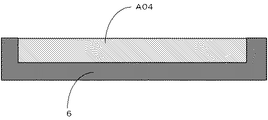
一方、基板6の溝の形成過程を図3を用いて説明する。図3は基板の溝の形成過程を説明する説明図であり、6は図1及び図2と同一符号を付してある。
On the other hand, the formation process of the groove | channel of the board |
例えば、基板6では図3中”A04”に示す部分がエッチング加工等により除去され、溝が形成される。
For example, in the
そして、流入口及び流出口が形成された基板4は、基板6に形成された溝の両端に図1中”IP110”及び”EP110”に示す流入口及び流出口が位置するように基板6と接着等により貼り合わされる。このような貼り合わせにより、基板6に形成された溝の開口部分は基板4で覆われ図1及び図2中”MF110”に示す微小流路を構成することになる。
The substrate 4 on which the inflow port and the outflow port are formed is connected to the
また、基板4に形成された図1中”IP110”に示す流入口からは複数個の触媒5が挿入され、図1及び図2中”MF110”に示す微小流路内に充填される。
Further, a plurality of
ここで、図1等に示す従来例を説明する。化学反応を行わせる液体は図1及び図2中”IP110”に示す流入口から注入され、図1及び図2中”MF110”に示す微小流路を流れる。 Here, a conventional example shown in FIG. A liquid for causing a chemical reaction is injected from the inlet indicated by “IP110” in FIGS. 1 and 2, and flows through a microchannel indicated by “MF110” in FIGS.
この時、液体は図1及び図2中”MF110”に示す微小流路に充填されている複数個の触媒5によって化学反応を起こし、化学反応を生じた液体が図1及び図2中”EP110”に示す流出口から排出される。
At this time, the liquid undergoes a chemical reaction by the plurality of
また、図1中”EP110”に示す流出口の口径は触媒5の直径より小さく形成されているので、複数個の触媒5は図1中”EP110”に示す流出口で堰き止められ、微小流路内に留まることになる。
Further, since the diameter of the outlet indicated by “EP110” in FIG. 1 is smaller than the diameter of the
この結果、2つの基板で構成される微小流路の一端に触媒の直径より口径が小さい流出口を設けることにより、簡単な構成で流路内に複数個の触媒を堰き止めることが可能になる。 As a result, by providing an outlet having a smaller diameter than the diameter of the catalyst at one end of the micro-channel constituted by two substrates, it becomes possible to dam up a plurality of catalysts in the channel with a simple configuration. .
図4及び図5は従来のマイクロチップの一例を示す平面図及び断面図である。また、図5は図4のA−A断面図である。 4 and 5 are a plan view and a cross-sectional view showing an example of a conventional microchip. FIG. 5 is a cross-sectional view taken along the line AA in FIG.
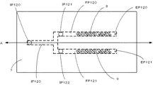
図4、図5において、7は流入口、触媒充填口及び流出口が形成された基板、8及び9は抗体が固着されたマイクロビーズ若しくは金属触媒を球状に形成した触媒、10は基板7と貼り合わされて流入流路及び充填流路を構成する溝が形成される基板である。また、触媒8及び9はそれぞれ種類が異なる触媒である。
4 and 5, 7 is a substrate on which an inlet, a catalyst filling port, and an outlet are formed, 8 and 9 are spherically formed microbeads or metal catalysts to which antibodies are fixed, and 10 is a substrate 7. It is a substrate on which grooves that are bonded together to form an inflow channel and a filling channel are formed.
例えば、基板7には図4中”IP120”に示す流入口、図4中”IP121”及び”IP122”に示す触媒充填口、図4中”EP120”及び”EP121”に示す流出口がエッチング加工等によりそれぞれ形成される。 For example, the substrate 7 is etched with an inlet indicated by “IP120” in FIG. 4, a catalyst filling port indicated by “IP121” and “IP122” in FIG. 4, and an outlet indicated by “EP120” and “EP121” in FIG. Etc., respectively.
この時、図4中”IP121”及び”IP122”に示す触媒充填口の口径は触媒8及び9の直径よりも大きく形成され、図4中”EP120”及び”EP121”に示す流出口の口径は触媒8及び9の直径よりも小さく形成される。
At this time, the diameters of the catalyst filling ports indicated by “IP121” and “IP122” in FIG. 4 are formed larger than the diameters of the
一方、基板10の溝の形成過程を図6を用いて説明する。図6は基板の溝の形成過程を説明する説明図であり、10は図5と同一符号を付してある。
On the other hand, the formation process of the groove | channel of the board |
例えば、基板10では図6中”A05”に示す部分がエッチング加工等により除去され、途中で分岐するような音叉型の形状をした溝が形成される。
For example, in the
そして、流入口、触媒充填口及び流出口が形成された基板7は、基板10と接着等により貼り合わされて、基板10に形成された溝の開口部分は基板7で覆われ図4中”IF120”に示す流入流路及び図4中”FP120”及び”FP121”に示す充填流路を構成することになる。
Then, the substrate 7 on which the inlet, the catalyst filling port, and the outlet are formed is bonded to the
また、図4中”IF120”に示す流入流路の一端は図4中”FP120”及び”FP121”に示す充填流路の一端と接続される。 Also, one end of the inflow channel indicated by “IF120” in FIG. 4 is connected to one end of the filling channel indicated by “FP120” and “FP121” in FIG.
この時、基板7に形成された図4中”IP120”に示す流入口が図4中”IF120”に示す流入流路の他端に、図4中”IP121”及び”IP122”に示す触媒充填口が図4中”FP120”及び”FP121”に示す充填流路上に、図4中”EP120”及び”EP121”に示す流出口が図4中”FP120”及び”FP121”に示す充填流路の他端に位置するように基板7及び基板10の配置が調整される。
At this time, the inflow port indicated by “IP120” in FIG. 4 formed on the substrate 7 is filled with the catalyst indicated by “IP121” and “IP122” in FIG. 4 at the other end of the inflow channel indicated by “IF120” in FIG. The outlet is shown in “FP120” and “FP121” in FIG. 4 and the outlet shown in “EP120” and “EP121” in FIG. 4 is the filling channel shown in “FP120” and “FP121” in FIG. The arrangement of the substrate 7 and the
基板7に形成された図4中”IP121”及び”IP122”に示す触媒充填口からは複数個の触媒8及び9がそれぞれ挿入され、図4中”FP120”及び”FP121”に示す充填流路内に充填される。
A plurality of
ここで、図4等に示す実施例を説明する。化学反応を行わせる液体は図4及び図5中”IP120”に示す流入口から注入され、図4中”IF120”に示す流入流路を流れる。 Here, the embodiment shown in FIG. 4 and the like will be described. The liquid for causing the chemical reaction is injected from the inlet indicated by “IP120” in FIGS. 4 and 5, and flows through the inflow channel indicated by “IF120” in FIG.
さらに、液体は図4中”IF120”に示す流入流路の一端で分岐され、図4中”FP120”及び”FP121”に示す充填流路をそれぞれ流れる。 Further, the liquid is branched at one end of the inflow channel indicated by “IF120” in FIG. 4 and flows through the filling channels indicated by “FP120” and “FP121” in FIG.
この時、液体は図4中”FP120”及び”FP121”に示す充填流路に充填されている複数個の触媒8及び9によってそれぞれ化学反応を起こし、化学反応を生じた液体が図4中”EP120”及び”EP121”に示す流出口からそれぞれ排出される。
At this time, the liquid undergoes a chemical reaction by the plurality of
また、図4中”EP120”及び”EP121”に示す流出口の口径は触媒8及び9の直径よりもそれぞれ小さく形成されているので、複数個の触媒8及び9は図4中”EP120”及び”EP121”に示す流出口でそれぞれ堰き止められ、微小流路内に留まることになる。
Further, since the diameters of the outlets indicated by “EP120” and “EP121” in FIG. 4 are formed smaller than the diameters of the
この結果、2つの基板で構成される2つの充填流路の一端に触媒の直径よりも口径が小さい流出口をそれぞれ設けることにより、簡単な構成で流路内に複数個の触媒を堰き止めることが可能になる。 As a result, a plurality of catalysts can be dammed in the flow path with a simple configuration by providing an outlet having a diameter smaller than the diameter of the catalyst at one end of the two filling flow paths composed of two substrates. Is possible.
また、それぞれ種類が異なる触媒が充填される2つの充填流路が形成されることにより、化学反応を促進させる触媒を選別することが出来る。 Further, by forming two filling channels filled with different types of catalysts, it is possible to select a catalyst that promotes a chemical reaction.
図7及び図8は本発明に係るマイクロチップの一実施例を示す平面図及び断面図である。図8は図7のA−A断面図である。 7 and 8 are a plan view and a cross-sectional view showing an embodiment of a microchip according to the present invention. 8 is a cross-sectional view taken along the line AA in FIG.
図7及び図8において、11は流入口及び流出口が形成された基板、12は抗体が固着されたマイクロビーズ若しくは金属触媒を球状に形成した触媒、13は基板11と貼り合わされて流入流路及び充填流路を構成する溝が形成された基板である。
7 and 8, 11 is a substrate on which an inlet and an outlet are formed, 12 is a microbead to which an antibody is fixed, or a catalyst in which a metal catalyst is formed in a spherical shape, and 13 is bonded to the
例えば、基板11には図7中”IP130”及び”IP131”に示す流入口、図7中”EP130”に示す流出口がエッチング加工等によりそれぞれ形成される。この時、図7中”IP130”及び”IP131”に示す流入口の口径は触媒12の直径よりもそれぞれ大きく形成され、図7中”EP130”に示す流出口の口径は触媒12の直径よりも小さく形成される。
For example, the
一方、基板13の溝の形成過程を図9を用いて説明する。図9は基板の溝の形成過程を説明する説明図であり、13は図8と同一符号を付してある。
On the other hand, the formation process of the groove | channel of the board |
例えば、基板13では図9中”A06”に示す部分がエッチング加工等により除去され、途中で合流するような音叉型の形状をした溝が形成される。
For example, in the
そして、流入口、及び流出口が形成された基板11は、基板13と接着等により貼り合わされて、基板13に形成された溝の開口部分は基板11で覆われ図7中”IF130”及び”IF131”に示す流入流路及び図7中”FP130”に示す充填流路を構成することになる。
Then, the
また、図7中”IF130”及び”IF131”示す流入流路の一端が図7中”FP130”に示す充填流路の一端と接続される。 Further, one end of the inflow channel indicated by “IF130” and “IF131” in FIG. 7 is connected to one end of the filling channel indicated by “FP130” in FIG.
この時、基板11に形成された図7中”IP130”及び”IP131”に示す流入口が図7中”IF130”及び”IF131”に示す流入流路の他端に、図7中”EP130”に示す流出口が図7中”FP130”に示す充填流路の他端に位置するように基板11及び基板13の配置が調整される。
At this time, the inflow port indicated by “IP130” and “IP131” in FIG. 7 formed on the
また、基板11に形成された図7中”IP130”及び”IP131”に示す流入口からは複数個の触媒12が挿入され、図7中”FP130”に示す充填流路内に充填される。
Further, a plurality of
ここで、図7等に示す実施例を説明する。化学反応を行わせる第1及び第2の液体は図7及び図8中”IP130”及び”IP131”に示す流入口からそれぞれ注入され、図7中”IF130”及び”IF131”に示す流入流路をそれぞれ流れる。 Here, the embodiment shown in FIG. 7 and the like will be described. The first and second liquids causing the chemical reaction are injected from the inlets indicated by “IP130” and “IP131” in FIGS. 7 and 8, respectively, and inflow passages indicated by “IF130” and “IF131” in FIG. Each flowing.
さらに、第1及び第2の液体は図7中”IF130”及び”IF131”に示す流入流路の他端でそれぞれ合流し、図7中”FP130”に示す充填流路を流れる。 Further, the first and second liquids merge at the other ends of the inflow passages indicated by “IF130” and “IF131” in FIG. 7, respectively, and flow through the filling passage indicated by “FP130” in FIG.
この時、第1及び第2の液体は図7中”FP130”に示す充填流路に充填されている複数個の触媒12によって化学反応を起こし、化学反応を生じた液体が図7”EP130”に示す流出口から排出される。
At this time, the first and second liquids cause a chemical reaction by the plurality of
また、図7中”EP130”に示す流出口の口径は触媒12の直径より小さく形成されているので、複数個の触媒12は図7中”EP130”に示す流出口で堰き止められ、微小流路内に留まることになる。
Further, since the diameter of the outlet indicated by “EP130” in FIG. 7 is smaller than the diameter of the
この結果、2つの基板で構成される充填流路の一端に触媒の直径より口径が小さい流出口を設けることにより、簡単な構成で流路内に複数個の触媒を堰き止めることが可能になる。 As a result, by providing an outlet having a smaller diameter than the diameter of the catalyst at one end of the filling channel constituted by two substrates, it becomes possible to dam up a plurality of catalysts in the channel with a simple configuration. .
また、第1及び第2の液体が合流して充填流路を流れることにより、種類の異なる液体が混合された液体を化学反応させることが可能となる。 In addition, when the first and second liquids merge and flow through the filling flow path, it is possible to cause a chemical reaction of the liquid in which different types of liquids are mixed.
図10及び図11は本発明に係るマイクロチップの一実施例を示す平面図及び断面図である。図11は図10のA−A断面図である。図12は本発明に係るマイクロチップの他の実施例を示す各基板の平面図である。図12(a)は基板14の平面図、図12(b)は基板17の平面図、図12(c)は基板18の平面図である。
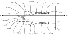
10 and 11 are a plan view and a cross-sectional view showing an embodiment of a microchip according to the present invention. 11 is a cross-sectional view taken along line AA in FIG. FIG. 12 is a plan view of each substrate showing another embodiment of the microchip according to the present invention. 12A is a plan view of the
図10及び図11において、14は流入口及び流出口が形成された基板、15及び16は抗体が固着されたマイクロビーズ若しくは金属触媒を球状に形成した触媒、17は基板14と貼り合わされて微小流路を構成する溝が形成された基板、18は基板17と貼り合わされて微小流路を構成する溝が形成された基板である。
10 and 11,
例えば、基板14には図10中”IP140”及び”IP143”に示す流入口、図10中”IP141”及び”IP142”に示す触媒充填口、”EP140”及び”EP141”に示す流出口がエッチング加工等によりそれぞれ形成される。
For example, the
この時、図10中”IP141”及び”IP142”に示す触媒充填口の口径は触媒15及び16の直径よりもそれぞれ大きく形成され、図10中”EP140”及び”EP141”に示す流出口の口径は触媒15及び16の直径よりもそれぞれ小さく形成される。
At this time, the diameters of the catalyst filling ports indicated by “IP141” and “IP142” in FIG. 10 are formed larger than the diameters of the
一方、基板17及び18の溝の形成過程を図13を用いて説明する。図13は基板の溝の形成過程を説明する説明図であり、図13(a)は基板17の斜視図、図13(b)は基板18の斜視図である。17及び18は図12と同一符号を付してある。
On the other hand, a process of forming grooves in the
例えば、基板17では図13中”A07”に示す部分がエッチング加工等により除去され、途中で分岐し分岐された2つの溝が他の2つの溝とそれぞれ合流するような溝が形成される。
For example, in the
また、基板18では図13中”A08”に示す部分がエッチング加工等により除去され、途中で分岐するような音叉型の形状をした溝が形成される。
Further, in the
そして、流入口、触媒充填口及び流出口が形成された基板14は、基板17と接着等により貼り合わされて、基板17に形成された溝の開口部分は基板14で覆われ図10中”IF140”に示す流入流路、図10中”FC140”、”FC141”、”FC142”及び”FC143”に示す流路、図10中”FP140”及び”FP141”に示す充填流路から構成される図10中”MF140”に示す微細流路を構成することになる。
Then, the
また、図10中”IF140”に示す流入流路の一端は図10中”FC140”及び”FC141”に示す流路の一端と接続され、図10中”FC140”、”FC141”、”FC142”及び”FC143”に示す流路の他端は図10中”FP140”及び”FP141”に示す充填流路の一端とそれぞれ接続される。 Further, one end of the inflow channel indicated by “IF140” in FIG. 10 is connected to one end of the channel indicated by “FC140” and “FC141” in FIG. 10, and “FC140”, “FC141”, “FC142” in FIG. The other end of the flow path indicated by “FC143” is connected to one end of a filling flow path indicated by “FP140” and “FP141” in FIG.
この時、基板14に形成された図10中”IP140”に示す流入口が図10中”IF140”に示す流入流路の他端に、図10中”IP141”及び”IP142”に示す触媒充填口が図10中”FP140”及び”FP141”に示す充填流路上に、図10中”EP140”及び”EP141”に示す流出口が図10中”FP140”及び”FP141”に示す充填流路の他端にそれぞれ位置するように基板14及び基板17の配置が調整される。
At this time, the inflow port indicated by “IP140” in FIG. 10 formed in the
さらに、基板14と接着された基板17は、基板18と接着等により貼り合わされて、基板18に形成された溝の開口部分は基板17で覆われ図10中”IF141”に示す流入流路、図10中”FC144”及び”FC145”に示す流路から構成される図10中”MF141”に示す微細流路を構成することになる。
Further, the
また、図10中”IF141”に示す流入流路の一端は図10中”FC144”及び”FC145”に示す流路の一端と接続される。 Also, one end of the inflow channel indicated by “IF141” in FIG. 10 is connected to one end of the channel indicated by “FC144” and “FC145” in FIG.
この時、基板17に形成された図10中”IP143”に示す流入口が図10中”IF141”に示す流入流路の一端に位置され、基板17に形成された図10中”FC142”及び”FC143”に示す流路の一端が図10中”FC144”及び”FC145”に示す流路の他端とそれぞれ接続されるように基板14及び基板17の配置が調整される。
At this time, the inflow port indicated by “IP143” in FIG. 10 formed in the
すなわち、図10中”FC142”及び”FC143”に示す流路の一端が図10中”FC144”及び”FC145”に示す流路の他端とそれぞれ接続されることにより、図10中”MF140”に示す微細流路及び図10中”MF141”に示す微細流路は相互に接続されることになる。 That is, one end of the flow path indicated by “FC142” and “FC143” in FIG. 10 is connected to the other end of the flow path indicated by “FC144” and “FC145” in FIG. And the fine flow path indicated by “MF141” in FIG. 10 are connected to each other.
また、基板14に形成された図10中”IP141”及び”IP142”に示す触媒充填口からは複数個の触媒15及び16がそれぞれ挿入され、図10中”FP140”及び”FP141”に示す充填流路内に充填される。
Further, a plurality of
ここで、図10等に示す実施例を説明する。化学反応を行わせる第1及び第2の液体は図10中”IP140”及び”IP143”に示す流入口からそれぞれ注入され、図10中”IF140”及び”IF141”に示す流入流路をそれぞれ流れる。 Here, the embodiment shown in FIG. 10 and the like will be described. The first and second liquids causing the chemical reaction are respectively injected from the inlets indicated by “IP140” and “IP143” in FIG. 10, and flow through the inflow passages indicated by “IF140” and “IF141” in FIG. .
第1の液体は図10中”IF140”に示す流入流路の他端で分岐して図10中”FC140”及び図10中”FC141”に示す流路をそれぞれ流れ、第2の液体は図10中”IF141”に示す流入流路の他端で分岐して図10中”FC144”及び図10中”FC145”に示す流路をそれぞれ流れる。 The first liquid branches at the other end of the inflow channel indicated by “IF140” in FIG. 10 and flows through the channels indicated by “FC140” in FIG. 10 and “FC141” in FIG. 10, respectively. 10 branches at the other end of the inflow channel indicated by “IF141” in FIG. 10 and flows through the channels indicated by “FC144” in FIG. 10 and “FC145” in FIG.
さらに、第2の液体は図10中”FC144”及び図10中”FC145”に示す流路から図10中”FC142”及び図10中”FC143”に示す流路に流れ込む。 Further, the second liquid flows from the flow path indicated by “FC144” in FIG. 10 and “FC145” in FIG. 10 to the flow path indicated by “FC142” in FIG. 10 and “FC143” in FIG.
第1と及び第2の液体は図10中”FC140”及び図10中”FC141”に示す流路の他端、図10中”FC142”及び”FC143”に示す流路の他端でそれぞれ合流し図10中”FP140”及び図10中”FP141”に示す充填流路をそれぞれ流れる。 The first and second liquids merge at the other ends of the flow paths indicated by “FC140” and “FC141” in FIG. 10 and at the other ends of the flow paths indicated by “FC142” and “FC143” in FIG. Then, it flows through the filling flow paths indicated by “FP140” in FIG. 10 and “FP141” in FIG.
この時、第1及び第2の液体は図10中”FP140”及び図10中”FP141”に示す充填流路に充填されている複数個の触媒15及び16によって化学反応を起こし、化学反応を生じた液体が図10中”EP140”及び”EP141”に示す流出口から排出される。
At this time, the first and second liquids cause a chemical reaction by the plurality of
また、図10中”EP140”及び”EP141”に示す流出口の口径は触媒15及び16の直径より小さく形成されているので、複数個の触媒15及び16は図10中”EP140”及び”EP141”に示す流出口で堰き止められ、充填流路内に留まることになる。
Further, since the diameters of the outlets indicated by “EP140” and “EP141” in FIG. 10 are smaller than the diameters of the
この結果、3つの基板で構成される2つの充填流路の一端に触媒の直径より口径が小さい流出口を設けることにより、簡単な構成で流路内に複数個の触媒を堰き止めることが可能になる。 As a result, by providing an outlet with a smaller diameter than the diameter of the catalyst at one end of the two filling channels composed of three substrates, it is possible to block a plurality of catalysts in the channel with a simple configuration. become.
また、2つの充填流路に第1及び第2の液体、種類が異なる触媒15及び16が充填されることにより、化学反応を促進させる触媒を選別することが出来る。
Moreover, the catalyst which accelerates | stimulates a chemical reaction can be selected by filling the two filling flow paths with the first and second liquids and the different types of
なお、図4等に示す実施例では、触媒8及び触媒9はそれぞれ種類が異なるものとしたが、特にこれに限定されるものではなく、触媒8及び触媒9はそれぞれ同じものであってもよい。この結果、触媒8及び触媒9がそれぞれ同じものであることにより、多量合成が可能となる。
In the embodiment shown in FIG. 4 and the like, the types of the
また、図4等に示す実施例では、図4中”IF120”に示す流入流路から図4中”FP120”及び”FP121”に示す充填流路に分岐される構成が例示されているが、特にこれに限定されるものではなく、3つ以上の充填流路に分岐される構成であってもよい。 Further, in the embodiment shown in FIG. 4 and the like, a configuration is illustrated in which the inflow passage shown by “IF120” in FIG. 4 is branched to the filling passage shown by “FP120” and “FP121” in FIG. It is not limited to this in particular, The structure branched to three or more filling flow paths may be sufficient.
また、図7等に示す実施例では、図7中”IF130”及び図7中”IF131”に示す流入流路の他端は図7中”FP130”に示す充填流路の他端とそれぞれ接続される構成が例示されているが、特にこれに限定されるものではなく、充填流路の他端は3つ以上の流入流路の一端と接続される構成であってもよい。 Further, in the embodiment shown in FIG. 7 and the like, the other end of the inflow passage shown by “IF130” in FIG. 7 and “IF131” in FIG. 7 is connected to the other end of the filling passage shown by “FP130” in FIG. However, the present invention is not particularly limited thereto, and the other end of the filling channel may be connected to one end of three or more inflow channels.
また、図1等に示す実施例では、図1中”EP110”に示す流出口は触媒の直径より口径が小さく形成されるとしているが、特にこれに限定されるものではなく、流出口の口径は触媒の最小径、若しくは、最小断面積よりも小さく形成されてもよい。 Further, in the embodiment shown in FIG. 1 and the like, the outlet shown as “EP110” in FIG. 1 is formed to have a smaller diameter than the diameter of the catalyst. May be formed smaller than the minimum diameter or the minimum cross-sectional area of the catalyst.
また、図3等に示す実施例では、図3中”IP121”に示す触媒充填口は触媒の直径より口径が大きく形成されるとしているが、特にこれに限定されるものではなく、触媒充填口の口径は触媒の最大径、若しくは、最大断面積よりも大きく形成されてもよい。 In the embodiment shown in FIG. 3 and the like, the catalyst filling port indicated by “IP121” in FIG. 3 is formed to have a diameter larger than the diameter of the catalyst. The diameter may be larger than the maximum diameter or the maximum cross-sectional area of the catalyst.
また、図10等に示す実施例では、図10中”FC140”及び”FC142”に示す流路の他端は図10中”FP140”に示す充填流路の他端と接続される構成が例示されているが、特にこれに限定されるものではなく、図10中”FC140”及び図10中”FC142”に示す流路の他端は2つ以上の流路に分岐し分岐された流路の一端が充填流路の一端とそれぞれ接続される構成であってもよい。 Further, in the embodiment shown in FIG. 10 and the like, a configuration in which the other end of the flow path indicated by “FC140” and “FC142” in FIG. 10 is connected to the other end of the filling flow path indicated by “FP140” in FIG. However, the present invention is not particularly limited to this, and the other end of the flow path indicated by “FC140” in FIG. 10 and “FC142” in FIG. 10 is branched into two or more flow paths. One end of each may be connected to one end of the filling channel.
また、図10等に示す実施例では、図10中”MF140”及び”MF141”に示す微細流路にそれぞれ種類が異なる液体が流れるとされているが、特にこれに限定されるものではなく、同じ液体が流れるものであってもよい。この結果、図10中”MF140”及び”MF141”に示す微細流路に同じ液体が流入されることにより、多量合成が可能となる。 Further, in the embodiment shown in FIG. 10 and the like, it is assumed that different types of liquids flow in the fine flow paths indicated by “MF140” and “MF141” in FIG. 10, but the present invention is not particularly limited thereto. The same liquid may flow. As a result, the same liquid flows into the fine flow channels indicated by “MF140” and “MF141” in FIG.
1、3、4、6、7、10、11、13、14、17、18 基板
2、5、8、9、12、15、16 触媒
1, 3, 4, 6, 7, 10, 11, 13, 14, 17, 18
Claims (6)
微小流路に充填される触媒と、A catalyst filled in a microchannel;
液体の流入口及び前記触媒の最小径よりも口径が小さい液体の流出口が形成された第1の基板と、A first substrate on which a liquid inlet and a liquid outlet having a diameter smaller than the minimum diameter of the catalyst are formed;
両端に前記流入口及び前記流出口が位置するように前記第1の基板と貼り合わされて前記微小流路を構成する溝が形成された第2の基板とA second substrate formed with grooves forming the microchannel by being bonded to the first substrate so that the inlet and the outlet are located at both ends;
を備えたことを特徴とするマイクロチップ。A microchip comprising:
前記触媒の最大径よりも大きいことを特徴とする
請求項1記載のマイクロチップ。 The inlet diameter is
The microchip according to claim 1, wherein the microchip is larger than a maximum diameter of the catalyst .
第1及び第2の充填流路に充填される第1及び第2の触媒と、First and second catalysts filled in the first and second filling channels;
液体の流入口及び前記第1及び前記第2の触媒の最小径よりもそれぞれ口径が小さい液体の第1及び第2の流出口が形成された第1の基板と、A first substrate on which a liquid inlet and a liquid first and second outlet having a diameter smaller than the minimum diameter of each of the first and second catalysts are formed;
前記第1の基板と貼り合わされて流入流路の一端に前記第1及び第2の充填流路の一端が接続される前記流入流路、前記第1及び第2の充填流路を構成し、前記流入流路の他端に前記流入口が、前記第1及び第2の充填流路の他端に前記第1及び第2の流出口がそれぞれ位置する溝が形成された第2の基板とThe inflow channel, which is bonded to the first substrate and one end of the first and second filling channels is connected to one end of the inflow channel, configure the first and second filling channels, A second substrate in which the inlet is formed at the other end of the inflow channel, and a groove in which the first and second outlets are positioned at the other end of the first and second filling channels;
を備えたことを特徴とするマイクロチップA microchip characterized by comprising
請求項3記載のマイクロチップ。The microchip according to claim 3.
充填流路に充填される触媒と、A catalyst filled in the filling channel;
液体の第1及び第2の流入口及び前記触媒の最小径よりも口径が小さい液体の流出口が形成された第1の基板と、A first substrate on which liquid first and second inlets and a liquid outlet having a diameter smaller than the minimum diameter of the catalyst are formed;
前記第1の基板と貼り合わされて第1及び第2の流入流路の一端に前記充填流路の一端が接続される前記第1及び第2の流入流路及び前記充填流路を構成し、前記第1及び第2の流入流路の他端に前記第1及び第2の流入口が、前記充填流路の他端に前記流出口がそれぞれ位置する溝が形成された第2の基板とThe first and second inflow channels and the filling channel are configured such that one end of the filling channel is connected to one end of the first and second inflow channels bonded to the first substrate, A second substrate on which the first and second inflow ports are formed at the other end of the first and second inflow channels, and a groove in which the outflow port is positioned at the other end of the filling channel;
を備えたことを特徴とするマイクロチップA microchip characterized by comprising
前記触媒の最大径よりもそれぞれ大きいことを特徴とするEach of which is larger than the maximum diameter of the catalyst.
請求項5記載のマイクロチップ。The microchip according to claim 5.
Priority Applications (1)
| Application Number | Priority Date | Filing Date | Title |
|---|---|---|---|
| JP2006234903A JP4848896B2 (en) | 2006-08-31 | 2006-08-31 | Microchip |
Applications Claiming Priority (1)
| Application Number | Priority Date | Filing Date | Title |
|---|---|---|---|
| JP2006234903A JP4848896B2 (en) | 2006-08-31 | 2006-08-31 | Microchip |
Publications (2)
| Publication Number | Publication Date |
|---|---|
| JP2008055309A JP2008055309A (en) | 2008-03-13 |
| JP4848896B2 true JP4848896B2 (en) | 2011-12-28 |
Family
ID=39238694
Family Applications (1)
| Application Number | Title | Priority Date | Filing Date |
|---|---|---|---|
| JP2006234903A Active JP4848896B2 (en) | 2006-08-31 | 2006-08-31 | Microchip |
Country Status (1)
| Country | Link |
|---|---|
| JP (1) | JP4848896B2 (en) |
Family Cites Families (4)
| Publication number | Priority date | Publication date | Assignee | Title |
|---|---|---|---|---|
| US6939632B2 (en) * | 2001-08-06 | 2005-09-06 | Massachusetts Institute Of Technology | Thermally efficient micromachined device |
| CN1764842B (en) * | 2003-03-24 | 2012-01-11 | 索尼株式会社 | Microchip, nucleic acid extracting kit, and nucleic acid extracting method |
| WO2006020709A1 (en) * | 2004-08-12 | 2006-02-23 | Velocys Inc. | Process for converting ethylene to ethylene oxide using microchannel process technology |
| JP2006087372A (en) * | 2004-09-24 | 2006-04-06 | Fuji Photo Film Co Ltd | Microdevice for separating and refining nucleic acid |
-
2006
- 2006-08-31 JP JP2006234903A patent/JP4848896B2/en active Active
Also Published As
| Publication number | Publication date |
|---|---|
| JP2008055309A (en) | 2008-03-13 |
Similar Documents
| Publication | Publication Date | Title |
|---|---|---|
| JP4685611B2 (en) | Microfluidic device | |
| Ji et al. | Silicon-based microfilters for whole blood cell separation | |
| JP3634868B2 (en) | Micro mixer | |
| CN107583692B (en) | Liquid drop micro-fluidic chip and preparation method thereof | |
| KR101097357B1 (en) | Multi function microfluidic flow control apparatus and multi function microfluidic flow control method | |
| JP2006346671A (en) | Liquid-liquid interface reactor | |
| JP4367283B2 (en) | Microfluidic chip | |
| JP2007139782A (en) | Device and method using fluid-transporting feature of differing dwell time | |
| US20060034735A1 (en) | Microreactor | |
| JP2006071388A (en) | Microchip and fluid control method in microchip | |
| JP6506907B2 (en) | Liquid handling device | |
| JP4848896B2 (en) | Microchip | |
| JP4868526B2 (en) | Sample introduction microdevice | |
| JP2009018311A (en) | Microfluid chip | |
| JP2006255583A (en) | Micro reactor | |
| JP2008132447A (en) | Microchip | |
| KR101689622B1 (en) | convergent-divergent micromixer using sinusoidal pulsatile flow and mixing method of fluid using the same | |
| JP4454431B2 (en) | plate | |
| JP2001091497A (en) | Free-flow electrophoresis device | |
| JP2005169218A (en) | Micro-mixer | |
| CN211111935U (en) | Microfluidic chip for preventing cell blockage by utilizing sheath fluid countercurrent | |
| JP2006075680A (en) | Multistage extraction chip | |
| JP2004202613A (en) | Microchannel chip | |
| JP2006051409A (en) | Micro-reactor | |
| WO2019044610A1 (en) | Particle separation device and particle separation apparatus using same |
Legal Events
| Date | Code | Title | Description |
|---|---|---|---|
| A621 | Written request for application examination |
Free format text: JAPANESE INTERMEDIATE CODE: A621 Effective date: 20090213 |
|
| A977 | Report on retrieval |
Free format text: JAPANESE INTERMEDIATE CODE: A971007 Effective date: 20100915 |
|
| A131 | Notification of reasons for refusal |
Free format text: JAPANESE INTERMEDIATE CODE: A131 Effective date: 20101007 |
|
| A521 | Request for written amendment filed |
Free format text: JAPANESE INTERMEDIATE CODE: A523 Effective date: 20101130 |
|
| TRDD | Decision of grant or rejection written | ||
| A01 | Written decision to grant a patent or to grant a registration (utility model) |
Free format text: JAPANESE INTERMEDIATE CODE: A01 Effective date: 20110920 |
|
| A01 | Written decision to grant a patent or to grant a registration (utility model) |
Free format text: JAPANESE INTERMEDIATE CODE: A01 |
|
| A61 | First payment of annual fees (during grant procedure) |
Free format text: JAPANESE INTERMEDIATE CODE: A61 Effective date: 20111003 |
|
| R150 | Certificate of patent or registration of utility model |
Ref document number: 4848896 Country of ref document: JP Free format text: JAPANESE INTERMEDIATE CODE: R150 Free format text: JAPANESE INTERMEDIATE CODE: R150 |
|
| FPAY | Renewal fee payment (event date is renewal date of database) |
Free format text: PAYMENT UNTIL: 20141028 Year of fee payment: 3 |
|
| R250 | Receipt of annual fees |
Free format text: JAPANESE INTERMEDIATE CODE: R250 |