JP4848324B2 - Serial-parallel conversion circuit and communication device - Google Patents
Serial-parallel conversion circuit and communication device Download PDFInfo
- Publication number
- JP4848324B2 JP4848324B2 JP2007183444A JP2007183444A JP4848324B2 JP 4848324 B2 JP4848324 B2 JP 4848324B2 JP 2007183444 A JP2007183444 A JP 2007183444A JP 2007183444 A JP2007183444 A JP 2007183444A JP 4848324 B2 JP4848324 B2 JP 4848324B2
- Authority
- JP
- Japan
- Prior art keywords
- data
- strobe
- clock
- serial
- register group
- Prior art date
- Legal status (The legal status is an assumption and is not a legal conclusion. Google has not performed a legal analysis and makes no representation as to the accuracy of the status listed.)
- Active
Links
Images


Classifications
-
- H—ELECTRICITY
- H03—ELECTRONIC CIRCUITRY
- H03M—CODING; DECODING; CODE CONVERSION IN GENERAL
- H03M9/00—Parallel/series conversion or vice versa
-
- H—ELECTRICITY
- H04—ELECTRIC COMMUNICATION TECHNIQUE
- H04L—TRANSMISSION OF DIGITAL INFORMATION, e.g. TELEGRAPHIC COMMUNICATION
- H04L12/00—Data switching networks
- H04L12/28—Data switching networks characterised by path configuration, e.g. LAN [Local Area Networks] or WAN [Wide Area Networks]
- H04L12/40—Bus networks
- H04L12/40052—High-speed IEEE 1394 serial bus
- H04L12/40117—Interconnection of audio or video/imaging devices
Landscapes
- Engineering & Computer Science (AREA)
- Multimedia (AREA)
- Computer Networks & Wireless Communication (AREA)
- Signal Processing (AREA)
- Theoretical Computer Science (AREA)
- Synchronisation In Digital Transmission Systems (AREA)
- Communication Control (AREA)
Description
本発明は、データとストローブに基づいて受信側でクロックを再生し、デコーディングを行うシリアルパラレル変換回路に関するものである。 The present invention relates to a serial-parallel conversion circuit that reproduces a clock on the receiving side based on data and a strobe and performs decoding.
従来、宇宙機器向けのインターフェース規格として、IEEE1355が知られている。また、近年、次世代の宇宙機器向けのインターフェース規格として「Space Wire」が提案されている。この「Space Wire」は、欧州宇宙機関(ESA: European Space Agency)によってIEEE1355をベースに宇宙標準として提案された規格であり、IEEE1355.2とも呼ばれている(例えば、特許文献1参照)。
また、地上では、AV機器やパソコン周辺機器等を統合して接続するのに適したインターフェースとして、IEEE1394高速シリアルバスが幅広く用いられている。
Conventionally, IEEE 1355 is known as an interface standard for space equipment. In recent years, “Space Wire” has been proposed as an interface standard for next-generation space equipment. This “Space Wire” is a standard proposed as a space standard based on IEEE 1355 by the European Space Agency (ESA), and is also referred to as IEEE 1355.2 (see, for example, Patent Document 1).
On the ground, an IEEE 1394 high-speed serial bus is widely used as an interface suitable for integrating and connecting AV devices and personal computer peripheral devices.
上述したIEEE1355、IEEE1355.2、IEEE1394等は、送信側から送られてきた「データ」、「ストローブ」の2つの信号から受信側で送信側のクロックを再現するため、送受信の両側でクロックを同期させる必要がなく、システムを安価に構成することが可能となる。また、データ転送レートが可変なため、様々な機器に柔軟に対応できる等の利点を有している。 The above-mentioned IEEE 1355, IEEE 1355.2, IEEE 1394, etc., synchronize the clocks on both sides of transmission and reception in order to reproduce the clock on the transmission side on the reception side from the two signals “data” and “strobe” sent from the transmission side. Therefore, the system can be configured at low cost. Further, since the data transfer rate is variable, there is an advantage that it can flexibly cope with various devices.
図15に、上記規格に用いられるシリアルパラレル変換回路の一構成例を示す。このようなシリアルパラレル変換回路では、送信側から受信した「データD」と「ストローブS」との排他的論理和をとることにより、クロックCLKが生成される。このクロックCLKは、シフトレジスタ100を構成する複数段のフリップフロップFF0,FF1,〜FFnに入力される。
これにより、図16に示すように、クロックCLKの立ち上がりで入力データDataがシフトレジスタ100の初段に設けられたフリップフロップFF0に取り込まれる。
As a result, as shown in FIG. 16, the input data Data is taken into the flip-flop FF0 provided at the first stage of the
ところで、図15に示したような従来のシリアルパラレル変換回路を実際の回路で実現する場合、クロックCLKや入力データDataがフリップフロップFF0に入力されるまでに遅延が生ずる。このとき、図17に示されるように、入力データDataが変化した後にクロックCLKがフリップフロップFF0に到達すれば問題は生じないが、図18に示されるように、入力データDataが変化する前にクロックCLKがフリップフロップFF0に到達してしまうと、変化する前のデータDataがフリップフロップFF0に取り込まれることとなり、本来取り込まれるべきデータと実際に取り込むデータとが異なるという、いわゆるレースコンディションが生ずる。 Incidentally, when the conventional serial-parallel conversion circuit as shown in FIG. 15 is realized by an actual circuit, a delay occurs until the clock CLK and the input data Data are input to the flip-flop FF0. At this time, as shown in FIG. 17, there is no problem if the clock CLK reaches the flip-flop FF0 after the input data Data changes, but before the input data Data changes as shown in FIG. When the clock CLK reaches the flip-flop FF0, the data Data before the change is taken into the flip-flop FF0, so that a so-called race condition occurs in which the data that should be taken in is different from the data that is actually taken in.
上記レースコンディションの問題を解消するために、遅延回路を介してクロックCLKをフリップフロップFF0に入力させることが考えられる。しかしながら、上述したシリアルパラレル変換回路をCPLD(Complex PLD)や、FPGA(Field Programmable Gate Array)等のプログラミング可能な汎用の半導体デバイスにより実現しようとすると、遅延回路を設けるのは非常に困難となる。
更に、遅延回路を設けることによりクロックCLKの位相を遅らせると、受信データの最小ビット周期がクロックCLKの遅延回路の遅延量によって制限されるため、最大受信速度もクロックCLKの遅延量により制限されてしまうという不都合が生ずる。
In order to solve the problem of the race condition, it is conceivable to input the clock CLK to the flip-flop FF0 through a delay circuit. However, if the serial-parallel conversion circuit described above is realized by a programmable general-purpose semiconductor device such as CPLD (Complex PLD) or FPGA (Field Programmable Gate Array), it is very difficult to provide a delay circuit.
In addition, if the phase of the clock CLK is delayed by providing a delay circuit, the minimum bit period of the received data is limited by the delay amount of the delay circuit of the clock CLK, so the maximum reception speed is also limited by the delay amount of the clock CLK. Inconvenience occurs.
本発明は、上記問題を解決するためになされたもので、受信速度を制約せずに、レースコンディションを解消することのできるシリアルパラレル変換回路の設計方法およびシリアルパラレル変換回路並びに通信装置を提供することを目的とする。 The present invention has been made to solve the above problems, and provides a serial-parallel conversion circuit design method, a serial-parallel conversion circuit, and a communication device that can eliminate race conditions without restricting the reception speed. For the purpose.
上記課題を解決するために、本発明は以下の手段を採用する。
本発明は、受信したデータとストローブとの排他的論理和をとることによりクロックを生成するクロック生成手段と、前記クロックの立ち上がりに同期してデータを取り込む第1のレジスタ群と、前記クロックの立ち下がりに同期してデータを取り込む第2のレジスタ群とを備えるシリアルパラレル変換回路において、前記第1のレジスタ群のデータ入力側に設けられるとともに、データとストローブとの組み合わせによって取り込むデータが一義的に決定される前記第1のレジスタ群の動作の規則性から定められる、データおよびストローブならびに前記第1のレジスタ群に取り込まれるデータの関係に従って、入力されたデータおよびストローブに対応する前記第1のレジスタ群に取り込まれるデータを出力する第1のデータ出力手段と、前記第2のレジスタ群のデータ入力側に設けられるとともに、データとストローブとの組み合わせによって取り込むデータが一義的に決定される前記第2のレジスタ群の動作の規則性から定められる、データおよびストローブならびに前記第2のレジスタ群に取り込まれるデータの関係に従って、入力されたデータおよびストローブに対応する前記第2のレジスタ群に取り込まれるデータを出力する第2のデータ出力手段と、前記第1のレジスタ群のデータ取り込みタイミングを前記クロックの立ち下がりとし、前記第2のレジスタ群のデータ取り込みタイミングを前記クロックの立ち上がりとするクロック反転手段とを具備するシリアルパラレル変換回路を提供する。
In order to solve the above problems, the present invention employs the following means.
The present invention includes a clock generation unit that generates a clock by taking an exclusive OR of received data and a strobe, a first register group that captures data in synchronization with a rising edge of the clock, and a rising edge of the clock. In a serial-parallel conversion circuit including a second register group that captures data in synchronization with a fall, the serial / parallel conversion circuit is provided on the data input side of the first register group, and the data to be captured is uniquely determined by a combination of data and a strobe. is determined is determined from the operating rule of the first group of registers, thus the data and strobe and said first taken into the register group relationship Lud over data, wherein corresponding to the input data and strobe a first data output means for outputting a captured Lud over data in the first register group Together provided to the data input side of the second register group, the data taking by the combination of the data and the strobe are determined from the operating rule of the second group of registers that are uniquely determined, the data and strobe and Thus the relation between the taken in the second register group Lud over data, a second data output means for outputting Lud over data taken into the second group of registers corresponding to the input data and strobe There is provided a serial / parallel conversion circuit comprising clock inversion means for setting the data fetch timing of the first register group as the fall of the clock and setting the data fetch timing of the second register group as the rise of the clock. .
発明者らは、受信したデータとストローブとの排他的論理和をとることにより、受信側でクロックを生成するようなシリアルパラレル変換回路において、レジスタ群に取り込まれるデータとストローブとの間には規則性があることを見出した。本発明は、このような規則性に着目して、データ受信の高速化と、レースコンディションを解消する点に特徴を有している。
即ち、このような構成によれば、第1レジスタ群および第2レジスタ群に入力するデータの有効期間を長めに設定する(例えば、従来の期間がクロック半周期分であったのに対し、本発明ではクロック1周期分、つまり、従来に比べてデータの有効期間を2倍とする)ことが可能となる。これにより、レーシング対策としてクロックに従来と同様の遅延回路を設けたとしても、従来に比べて高速なシリアルデータをパラレルデータに変換することが可能となる。
特に、シリアルパラレル変換回路を通信装置に用いる場合には、シリアルパラレル変換装置においてメモリ素子がデータを取り込むのに必要な時間が通信速度の律速点になるので、通信速度(ビットレート)を約2倍とすることが可能となる。
また、このようにすることで、遅延回路を不要とすることができ、より高速なシリアルパラレル変換を実現することが可能となる。
In the serial-parallel conversion circuit in which a clock is generated on the receiving side by taking an exclusive OR of the received data and the strobe, the inventors have a rule between the data and the strobe taken in the register group. I found that there is sex. The present invention pays attention to such regularity, and is characterized by speeding up of data reception and elimination of race conditions.
That is, according to such a configuration, the effective period of data input to the first register group and the second register group is set to be longer (for example, the conventional period is a half cycle of the clock, whereas In the present invention, it is possible to double the effective period of data for one clock cycle, that is, compared to the conventional case. As a result, even if a delay circuit similar to the conventional one is provided in the clock as a countermeasure against racing, it is possible to convert serial data that is faster than the conventional one into parallel data.
In particular, when a serial / parallel conversion circuit is used in a communication device, the time required for the memory element to capture data in the serial / parallel conversion device becomes the rate limiting point of the communication speed, so the communication speed (bit rate) is about 2 It becomes possible to double.
In addition, by doing so, a delay circuit can be omitted, and higher-speed serial / parallel conversion can be realized.
上記シリアルパラレル変換回路において、前記第1のデータ出力手段は、データが0およびストローブが1のときに0を出力し、データが1およびストローブが0のときに1を出力し、データとストローブとがともに0またはともに1のときに前回値を出力し、前記第2のデータ出力手段は、データが0およびストローブが0のときに0を出力し、データが1およびストローブが1のときに1を出力し、データとストローブとが互いに異なる値をとるときに前回値を出力することとしてもよい。
In the serial-parallel conversion circuit, said first data output means,
本発明は、受信したデータとストローブとの排他的論理和をとることにより、クロックを生成するクロック生成手段と、前記クロックの立ち下がりでデータを取り込む第1のレジスタ群と、前記クロックの立ち上がりでデータを取り込む第2のレジスタ群と、前記第1のレジスタ群のデータ入力側に設けられ、データが0およびストローブが1のときに0を出力し、データが1およびストローブが0のときに1を出力し、データとストローブとがともに0またはともに1のときに前回値を出力する第1のデータ出力手段と、前記第2のレジスタ群のデータ入力側に設けられ、データが0およびストローブが0のときに0を出力し、データが1およびストローブが1のときに1を出力し、データとストローブとが互いに異なる値をとるときに前回値を出力する第2のデータ出力手段とを具備するシリアルパラレル変換回路を提供する。
The present invention provides a clock generating means for generating a clock by taking an exclusive OR of received data and a strobe, a first register group for capturing data at the falling edge of the clock, and a rising edge of the clock. A second register group for fetching data and provided on the data input side of the first register group,
このような構成によれば、クロックの立ち上がりで第1のレジスタ群において最初に信号が入力されるメモリ素子に取り込まれるデータが変化し、このデータをクロックの立下りで該メモリ素子が取り込む。同様に、クロックの立下りで第2のレジスタ群において最初に信号が入力されるメモリ素子に取り込まれるデータが変化し、このデータをクロックの立ち上がりで該メモリ素子が取り込む。このように、各レジスタ群における最初に信号が入力されるメモリ素子がデータを取り込むタイミングと、該メモリ素子が取り込むデータが変化するタイミングとが略半周期ずれているので、変化後のデータを確実にメモリ素子に読み取らせることが可能となる。 According to such a configuration, the data captured in the memory element to which a signal is first input in the first register group changes at the rising edge of the clock, and the data is captured by the memory element at the falling edge of the clock. Similarly, the data fetched into the memory element to which a signal is first input in the second register group changes at the fall of the clock, and the memory element takes in this data at the rise of the clock. In this way, the timing at which the memory element to which a signal is first input in each register group captures data is shifted from the timing at which the data captured by the memory element changes by approximately half a cycle, so that the data after the change is reliably Can be read by the memory element.
本発明において、上記第1のレジスタ群および第2のレジスタ群は、例えば、複数のメモリ素子が直列、或いは、並列に接続されて構成されていてもよい。
本発明は、上記シリアルパラレル変換回路を備える通信装置を提供する。
また、上記態様は、可能な範囲で組み合わせて利用することができるものである。
In the present invention, the first register group and the second register group may be configured, for example, by connecting a plurality of memory elements in series or in parallel.
The present invention provides a communication device including the serial-parallel conversion circuit .
Moreover, the said aspect can be utilized combining in the possible range.
本発明によれば、受信速度を制約せずに、レースコンディションを解消することができるという効果を奏する。 According to the present invention, it is possible to eliminate the race condition without restricting the reception speed.
以下に、本発明に係るシリアルパラレル変換回路の設計方法およびシリアルパラレル変換回路および通信装置並びにプログラムの一実施形態について、図面を参照して説明する。 Hereinafter, an embodiment of a serial-parallel conversion circuit design method, a serial-parallel conversion circuit, a communication device, and a program according to the present invention will be described with reference to the drawings.
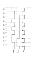
図1には、レジスタ群として複数のメモリ素子が直列に接続されて構成されるシフトレジスタを用いた場合のシリアルパラレル変換回路の概略構成が示されている。図1に示されるように、シリアルパラレル変換回路1は、送信機(図示略)から受信したデータDとストローブSとの排他的論理和(イクスクルーシブOR)をとることにより、クロックCLKを生成するクロック生成部2と、該クロックCLKに同期してデータを取り込む第1のシフトレジスタSF1および第2のシフトレジスタSF2を有している。
第1のシフトレジスタ(第1のレジスタ群)SF1は、直列に接続されたn段のDフリップフロップ(メモリ素子)10a,10b・・・10nを備えている。第1のシフトレジスタSF1は、クロックCLKの立ち上がりでデータDを取り込む構成とされている。第1のシフトレジスタSF1において、初段のDフリップフロップ10aに取り込まれたデータDは、下段のDフリップフロップ10b・・・10nに順次取り込まれ、最終的にnビットのパラレルデータとして出力される。
FIG. 1 shows a schematic configuration of a serial-parallel conversion circuit when a shift register configured by connecting a plurality of memory elements in series as a register group is used. As shown in FIG. 1, the serial-
The first shift register (first register group) SF1 includes n stages of D flip-flops (memory elements) 10a, 10b,..., 10n connected in series. The first shift register SF1 is configured to capture the data D at the rising edge of the clock CLK. In the first shift register SF1, the data D fetched by the first stage D flip-
第2のシフトレジスタ(第2のレジスタ群)SF2は、直列に接続されたn段のDフリップフロップ(メモリ素子)20a,20b・・・20nを備えている。第2のシフトレジスタSF2は、クロックCLKの立ち下がりでデータDを取り込む構成とされている。第2のシフトレジスタSF2において、初段のDフリップフロップ20aに取り込まれたデータDは、下段のDフリップフロップ20b・・・20nに順次取り込まれ、最終的にnビットのパラレルデータとして出力される。
なお、本実施形態では、各メモリ素子が直列に接続されている場合について例示したが、これらのメモリ素子は並列に接続されていてもよい。また、本発明におけるレジスタ群は、上記シフトレジスタに限定されず、シリアルパラレル変換に用いられる公知の他の構成とされていてもよい。
The second shift register (second register group) SF2 includes n stages of D flip-flops (memory elements) 20a, 20b,... 20n connected in series. The second shift register SF2 is configured to capture the data D at the falling edge of the clock CLK. In the second shift register SF2, the data D captured by the first stage D flip-
In the present embodiment, the case where the memory elements are connected in series has been illustrated, but these memory elements may be connected in parallel. In addition, the register group in the present invention is not limited to the above-described shift register, and may be another known configuration used for serial / parallel conversion.
図2には、図1に示されたシリアルパラレル変換回路1のタイミングチャートが示されている。図2に示されるように、クロックCLKの立ち上がりで、シリアルデータDが第1のシフトレジスタSF1のDフリップフロップ10aに取り込まれ、クロックCLKの立下りでシリアルデータDが第2のシフトレジスタSF2のDフリップフロップ20aに取り込まれる。このように、シリアルパラレル変換回路1は、クロックCLKの立ち上がりおよび立下りに同期して、シリアルデータDを第1のシフトレジスタSF1および第2のシフトレジスタSF2に交互に取り込むので、受信速度を高速化することができるという利点を有している。
FIG. 2 shows a timing chart of the serial-
ところで、図1に示したシリアルパラレル変換回路1は、レースコンディションの問題を抱えている。
即ち、図1に示したシリアルパラレル変換回路1においては、データDが変化した後に、クロックCLKがDフリップフロップ10a、20aに到達するという補償がない。このため、図3に示されるように、クロックCLKがデータDよりも先にDフリップフロップ10a、20aに到達してしまった場合には、変化する前のデータDがDフリップフロップ10a,20aに取り込まれることとなり、本来取り込まれるべきデータと実際に取り込まれるデータとが異なってしまう。
Incidentally, the serial-
That is, in the serial-
このようなレースコンディションを解消するべく、本実施形態に係るシリアルパラレル変換回路の設計方法では、以下のような論理回路を設けることとしている。
具体的には、まず、第1のシフトレジスタSF1の初段のDフリップフロップ10aの動作に着目し、このDフリップフロップ10aがデータを保持するときのデータおよびストローブの論理値が略同時に変化しないことが担保されることに基づく規則性を求め、該規則性に合致する出力を行う論理回路(第1の論理回路)を第1のシフトレジスタSF1の入力側に設け、更に、第1のシフトレジスタSF1を構成するn段のDフリップフロップ10a〜10nのうち、少なくとも初段のDフリップフロップ10aのデータ取り込みタイミングを半周期ずらす、つまり、立下りでデータDを取り込むこととする。
In order to eliminate such a race condition, the serial-parallel conversion circuit design method according to the present embodiment is provided with the following logic circuit.
Specifically, first, paying attention to the operation of the first stage D flip-
また、同様に、第2のシフトレジスタSF2の初段のDフリップフロップ20aの動作に着目し、このDフリップフロップ20aがデータを保持するときのデータおよびストローブの論理値が略同時に変化しないことが担保されることに基づく規則性を求め、該規則性に合致する出力を行う論理回路(第2の論理回路)を第2のシフトレジスタSF2の入力側に設け、更に、第2のシフトレジスタSF2を構成するn段のDフリップフロップ20a〜20nのうち、少なくとも初段のDフリップフロップ20aのデータ取り込みタイミングを半周期ずらす、つまり、立ち上がりでデータDを取り込むこととする。
Similarly, paying attention to the operation of the first stage D flip-
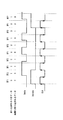
これにより、例えば、図1に示されたシリアルパラレル変換回路1は、図4に示されるようなシリアルパラレル変換回路1´とされる。
図4において、符号30は、Dフリップフロップ10aの動作の規則性に従った出力を行う論理回路(第1の論理回路)、符号40は、Dフリップフロップ20aの動作の規則性に従った出力を行う論理回路(第2の論理回路)である。また、第1のシフトレジスタSF1を構成する各Dフリップフロップ10a〜10nのクロック入力ラインには、クロックCLKを反転するための反転回路50a〜50nがそれぞれ設けられている。これにより、Dフリップフロップ10a〜10nは、クロックCLKの立下りタイミングで論理回路30から出力されるデータDevenを順次取り込むこととなる。
また、第2のシフトレジスタSF2を構成する各Dフリップフロップ20a〜20nのクロック入力ラインから反転回路を取り去ることで、Dフリップフロップ20a〜20nのデータDの取り込みタイミングをクロックCLKの立上がりとしている。
Thereby, for example, the serial-
In FIG. 4,
Further, by removing the inverting circuit from the clock input line of each of the D flip-
次に、上記論理回路30について詳細に説明する。
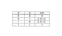
まず、図1に示したDフリップフロップ10aの動作に着目すると、クロックCLKの立ち上がりでデータDを取り込み、次のCLKの立ち上がりまで取り込んだデータDを保持する。クロックCLKが立ち上がるとき、つまり、排他的論理和ExORの出力が「1」となるのは、データDが「1」およびストローブSが「0」のときと、データDが「0」およびストローブSが「1」のときである。また、排他的論理和ExORの出力が「0」となるのは、データDとストローブSとが同じ値をとるときである。図5に、上記Dフリップフロップ10aの動作の規則性を示す。
Next, the
First, paying attention to the operation of the D flip-
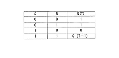
図5からわかるように、データDが「0」およびストローブSが「1」のときには、Dフリップフロップ10aに入力されるべきデータDは必ず「0」であり、データDが「1」およびストローブSが「0」のときには、Dフリップフロップ10aに入力されるべきデータDは必ず「1」である。また、これ以外の場合には、前回値Z(T−1)が保持される。
As can be seen from FIG. 5, when the data D is “0” and the strobe S is “1”, the data D to be input to the D flip-
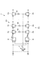
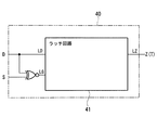
図6には、図5に示すような規則性と合致する出力を生成する論理回路30の一構成例が示されている。
図6に示されるように、論理回路30は、2つの入力端子LD,LGと、1つの出力端子LZを有するラッチ回路31を有している。ラッチ回路31の入力端子LDには、データDが入力され、入力端子LGにはデータDとストローブSとの排他的論理和をとった信号が入力されるようになっている。
このような構成によれば、データDとストローブSとの値が異なる場合に、データDが出力端子LZから出力され、データDとストローブSとの値が同一の場合に、前回値Z(T−1)が保持される。
FIG. 6 shows a configuration example of the
As illustrated in FIG. 6, the
According to such a configuration, when the data D and the strobe S have different values, the data D is output from the output terminal LZ, and when the data D and the strobe S have the same value, the previous value Z (T -1) is retained.
なお、論理回路30は、上記構成例に限られず、組み合わせ論理により容易に実現することが可能である。例えば、図7および図9に示されるようなRSフリップフロップ(RSラッチ)等を用いることにより図19および図20に示すように容易に実現することができる。図8には図7に示したRSフリップフロップの真理値表が、図10には図9に示したRSフリップフロップの真理値表が示されている。
Note that the
次に、上記論理回路40について詳細に説明する。
Dフリップフロップ20aの動作に着目すると、クロックCLKの立下りでデータDを取り込み、次のクロックCLKの立下りまで取り込んだデータDを保持する。クロックCLKが立ち下がるとき、つまり、排他的論理和ExORの出力が「0」となるのは、データDが「0」およびストローブSが「0」のときと、データDが「1」およびストローブSが「1」のときである。また、排他的論理和ExORの出力が「0」となるのは、データDとストローブSとが異なる値をとるときである。図11に、上記Dフリップフロップ20aの動作の規則性を表す。
Next, the
Focusing on the operation of the D flip-
図11からわかるように、データDが「0」およびストローブSが「0」のときには、Dフリップフロップ20aに入力されるべきデータDは必ず「0」であり、データDが「1」およびストローブSが「1」のときには、Dフリップフロップ20aに入力されるべきデータDは必ず「1」である。また、これ以外の場合には、前回値Z(T−1)が保持される。
As can be seen from FIG. 11, when the data D is “0” and the strobe S is “0”, the data D to be input to the D flip-
図12には、図11に示される規則性に合致する出力を生成する論理回路40の一構成例が示されている。
図12に示されるように、論理回路40は、2つの入力端子LD,LGと、1つの出力端子LZを有するラッチ回路41を有している。このラッチ回路41は、例えば、図6に示したラッチ回路31と同様の構成を有している。ラッチ回路41の入力端子LDには、データDが入力され、入力端子LGにはデータDとストローブSとの排他的論理和を反転させた信号が入力されるようになっている。
このような構成によれば、データDとストローブSとの値が同一の場合に、データDが出力端子LZから出力され、データDとストローブSとの値が異なる場合に、前回値Z(T−1)が保持される。
なお、論理回路40は、上記構成例に限られず、組み合わせ論理により容易に実現することが可能である。例えば、図7および図9に示されるようなRSフリップフロップ(RSラッチ)等を用いることにより図21および図22に示すように容易に実現することができる。
FIG. 12 shows a configuration example of the
As shown in FIG. 12, the
According to such a configuration, when the data D and the strobe S have the same value, the data D is output from the output terminal LZ, and when the data D and the strobe S have different values, the previous value Z (T -1) is retained.
The
図13には、図4に示されたシリアルパラレル変換回路、つまり、本発明の一実施形態に係るシリアルパラレル変換回路のタイミングチャートが示されている。
図13に示されるように、クロックCLKの立下りの略半周期前には、論理回路30の出力DevenはデータDに応じて既に変化し、かつ出力Devenは次のクロックCLKの立上がりまで保持されているので、クロックCLKの位相が伝送ライン等の要因により多少ずれたとしても、Dフリップフロップ10aは、取り込まれるべきデータを確実に取り込むことが可能となる。同様に、クロックCLKの立ち上がりの略半周期前には、論理回路40の出力DoddはデータDに応じて既に変化し、かつ出力Doddは次のクロックCLKの立下がりまで保持されているので、クロックCLKの位相が伝送ライン等の要因により多少ずれたとしても、Dフリップフロップ20aは、取り込むべきデータを確実に取り込むことが可能となる。
FIG. 13 shows a timing chart of the serial-parallel conversion circuit shown in FIG. 4, that is, the serial-parallel conversion circuit according to one embodiment of the present invention.
As shown in FIG. 13, approximately half a cycle before the fall of the clock CLK, the output Deven of the
以上説明してきたように、本実施形態に係るシリアルパラレル変換回路の設計方法およびシリアルパラレル変換回路1´によれば、図13に示されるように、データが変化するタイミングとデータを取り込むタイミングとを半周期ずらすこととしたので、変化後のデータを確実に初段のフリップフロップ10a,20aに取り込ませることが可能となる。これにより、レースコンディションの問題を解消することができる。
更に、遅延回路を採用していないことから、本実施形態に係るシリアルパラレル変換回路をCPLD(Complex PLD)や、FPGA(Field Programmable Gate Array)等のプログラミング可能な汎用の半導体デバイスにより容易に実現することが可能となる。更に、遅延回路とは別の方法でレースコンディションの問題を解消することにより、受信速度が制約されず、通信環境に応じた最適かつ高速なビットレートで通信を行うことが可能となる。
As described above, according to the serial-parallel conversion circuit design method and the serial-
Furthermore, since the delay circuit is not employed, the serial-parallel conversion circuit according to the present embodiment is easily realized by a programmable general-purpose semiconductor device such as CPLD (Complex PLD) or FPGA (Field Programmable Gate Array). It becomes possible. Further, by eliminating the race condition problem by a method different from the delay circuit, the reception speed is not restricted, and communication can be performed at an optimum and high bit rate according to the communication environment.
なお、上述した本実施形態では、Dフリップフロップを用いてnビットのシフトレジスタを構成したが、シフトレジスタの構成はこれに限られない。例えば、JKフリップフロップ等の他のメモリ素子を用いてシフトレジスタを構成することとしてもよい。
また、シフトレジスタを構成する各メモリ素子は、必ずしも同一のタイミングでデータを取り込まなくてもよい。例えば、図4において、初段のフリップフロップ10aがクロックCLKの立ち下がりでデータDevenを取り込むのに対し、他のフリップフロップ10b〜10nはクロックCLKの立ち上がりで前段のDフリップフロップからのデータを取り込むような構成としてもよい。
更に、本実施形態では、シフトレジスタを使用した場合について例示したが、これ以外のレジスタを用いてシリアルパラレル変換回路を構成することとしてもよい。
In the present embodiment described above, an n-bit shift register is configured using D flip-flops, but the configuration of the shift register is not limited thereto. For example, the shift register may be configured using another memory element such as a JK flip-flop.
In addition, each memory element included in the shift register does not necessarily have to capture data at the same timing. For example, in FIG. 4, the first flip-
Furthermore, although the case where a shift register is used is illustrated in the present embodiment, the serial / parallel conversion circuit may be configured using a register other than this.
また、上述した本実施形態に係るシリアルパラレル変換回路1´は、通信装置に利用されて好適なものである。通信装置としては、ルータ、コンピュータ間データ通信端末、機器間のデータ通信端末、リモートセンシング用通信装置、リモートコントロール用通信装置、データストレージ用通信装置等が一例として挙げられる。また、通信装置は、地上で用いられるものに限られず、宇宙を含む様々な環境下で用いられるものも含む。
The serial-
また、図4に示した本発明の一実施形態に係るシリアルパラレル変換回路1´をCPLD(Complex PLD)や、FPGA(Field Programmable Gate Array)等のプログラミング可能な汎用の半導体デバイスにより実現する場合には、ハードウェア記述言語等によりハードウェア設計を行う。ハードウェア記述言語の一例としては、VHDLやVerlog−HDL等が挙げられる。 4 is realized by a programmable general-purpose semiconductor device such as CPLD (Complex PLD) or FPGA (Field Programmable Gate Array). Performs hardware design using a hardware description language or the like. Examples of hardware description languages include VHDL and Verlog-HDL.
上記シリアルパラレル変換回路1´の一部をVHDLにより表したときの一例を図14に示す。このように、VHDL等のハードウェア記述言語を用いてプログラミングを行うことにより、図4に示した本実施形態に係るシリアルパラレル変換回路1´を容易に実現することが可能となる。なお、図14では、図4に示されたフリップフロップ10aが「FF0」として、フリップフロップ10bが「FF2」として記述されている。
FIG. 14 shows an example when a part of the serial-
以上、本発明の実施形態について図面を参照して詳述してきたが、具体的な構成はこの実施形態に限られるものではなく、本発明の要旨を逸脱しない範囲の設計変更等も含まれる。 As mentioned above, although embodiment of this invention was explained in full detail with reference to drawings, the specific structure is not restricted to this embodiment, The design change etc. of the range which does not deviate from the summary of this invention are included.
1 回路変更前のシリアルパラレル変換回路
1´ シリアルパラレル変換回路
2 クロック生成部
SF1 第1のシフトレジスタ
SF2 第2のシフトレジスタ
30,40 論理回路
10a〜10n,20a〜20n Dフリップフロップ
50a〜50n 反転回路
DESCRIPTION OF
Claims (4)
前記第1のレジスタ群のデータ入力側に設けられるとともに、データとストローブとの組み合わせによって取り込むデータが一義的に決定される前記第1のレジスタ群の動作の規則性から定められる、データおよびストローブならびに前記第1のレジスタ群に取り込まれるデータの関係に従って、入力されたデータおよびストローブに対応する前記第1のレジスタ群に取り込まれるデータを出力する第1のデータ出力手段と、
前記第2のレジスタ群のデータ入力側に設けられるとともに、データとストローブとの組み合わせによって取り込むデータが一義的に決定される前記第2のレジスタ群の動作の規則性から定められる、データおよびストローブならびに前記第2のレジスタ群に取り込まれるデータの関係に従って、入力されたデータおよびストローブに対応する前記第2のレジスタ群に取り込まれるデータを出力する第2のデータ出力手段と、
前記第1のレジスタ群のデータ取り込みタイミングを前記クロックの立ち下がりとし、前記第2のレジスタ群のデータ取り込みタイミングを前記クロックの立ち上がりとするクロック反転手段と
を具備するシリアルパラレル変換回路。 Clock generating means for generating a clock by taking an exclusive OR of the received data and the strobe, a first register group for taking in data in synchronization with the rising edge of the clock, and in synchronization with the falling edge of the clock A serial-parallel conversion circuit including a second register group for capturing data
Together provided to the data input side of said first register group, the data taking by the combination of the data and the strobe are determined from the operating rule of the first group of registers that are uniquely determined, the data and strobe and Thus the relation between the taken in the first register group Lud over data, a first data output means for outputting the Lud over data taken into the first register group corresponding to the input data and strobe ,
Data and strobes provided on the data input side of the second register group and defined by the regularity of operation of the second register group in which the data to be captured is uniquely determined by the combination of the data and the strobe; and Thus the relation between the taken in the second register group Lud over data, a second data output means for outputting Lud over data taken into the second group of registers corresponding to the input data and strobe ,
A serial-parallel conversion circuit comprising clock inversion means for setting the data fetch timing of the first register group as the fall of the clock and setting the data fetch timing of the second register group as the rise of the clock.
前記第2のデータ出力手段は、データが0およびストローブが0のときに0を出力し、データが1およびストローブが1のときに1を出力し、データとストローブとが互いに異なる値をとるときに前回値を出力する請求項1に記載のシリアルパラレル変換回路。 The first data output means outputs 0 when the data is 0 and the strobe is 1, outputs 1 when the data is 1 and the strobe is 0, and both the data and the strobe are 0 or 1 When the previous value is output,
The second data output means outputs 0 when the data is 0 and the strobe is 0, outputs 1 when the data is 1 and the strobe is 1, and the data and the strobe have different values. serial-parallel conversion circuit according to claim 1 which outputs a previous value.
前記クロックの立ち下がりでデータを取り込む第1のレジスタ群と、
前記クロックの立ち上がりでデータを取り込む第2のレジスタ群と、
前記第1のレジスタ群のデータ入力側に設けられ、データが0およびストローブが1のときに0を出力し、データが1およびストローブが0のときに1を出力し、データとストローブとがともに0またはともに1のときに前回値を出力する第1のデータ出力手段と、
前記第2のレジスタ群のデータ入力側に設けられ、データが0およびストローブが0のときに0を出力し、データが1およびストローブが1のときに1を出力し、データとストローブとが互いに異なる値をとるときに前回値を出力する第2のデータ出力手段と
を具備するシリアルパラレル変換回路。 A clock generating means for generating a clock by taking an exclusive OR of the received data and the strobe;
A first register group for capturing data at the falling edge of the clock;
A second register group for capturing data at the rising edge of the clock;
Provided on the data input side of the first register group, outputs 0 when the data is 0 and the strobe is 1 , outputs 1 when the data is 1 and the strobe is 0, and both the data and the strobe First data output means for outputting a previous value when both 0 or 1;
Provided on the data input side of the second register group, outputs 0 when the data is 0 and the strobe is 0, outputs 1 when the data is 1 and the strobe is 1, and the data and the strobe A serial-parallel conversion circuit comprising second data output means for outputting a previous value when taking different values.
Priority Applications (3)
| Application Number | Priority Date | Filing Date | Title |
|---|---|---|---|
| JP2007183444A JP4848324B2 (en) | 2007-07-12 | 2007-07-12 | Serial-parallel conversion circuit and communication device |
| US12/216,753 US7692564B2 (en) | 2007-07-12 | 2008-07-10 | Serial-to-parallel conversion circuit and method of designing the same |
| EP08160241.9A EP2015457B1 (en) | 2007-07-12 | 2008-07-11 | Serial-to-parallel conversion circuit and method of designing the same |
Applications Claiming Priority (1)
| Application Number | Priority Date | Filing Date | Title |
|---|---|---|---|
| JP2007183444A JP4848324B2 (en) | 2007-07-12 | 2007-07-12 | Serial-parallel conversion circuit and communication device |
Publications (2)
| Publication Number | Publication Date |
|---|---|
| JP2009021866A JP2009021866A (en) | 2009-01-29 |
| JP4848324B2 true JP4848324B2 (en) | 2011-12-28 |
Family
ID=39880968
Family Applications (1)
| Application Number | Title | Priority Date | Filing Date |
|---|---|---|---|
| JP2007183444A Active JP4848324B2 (en) | 2007-07-12 | 2007-07-12 | Serial-parallel conversion circuit and communication device |
Country Status (3)
| Country | Link |
|---|---|
| US (1) | US7692564B2 (en) |
| EP (1) | EP2015457B1 (en) |
| JP (1) | JP4848324B2 (en) |
Families Citing this family (5)
| Publication number | Priority date | Publication date | Assignee | Title |
|---|---|---|---|---|
| CN103888147B (en) * | 2014-04-09 | 2017-08-22 | 龙迅半导体(合肥)股份有限公司 | A kind of transformation from serial to parallel change-over circuit and converter and converting system |
| US20170257795A1 (en) * | 2014-10-27 | 2017-09-07 | Intel IP Corporation | Wireless device, method, and computer readable media for compressed media access control header |
| US10423565B2 (en) * | 2016-10-13 | 2019-09-24 | SK Hynix Inc. | Data transmission systems having a plurality of transmission lanes and methods of testing transmission data in the data transmission systems |
| CN113078909B (en) * | 2021-03-23 | 2023-01-31 | 汕头市超声检测科技有限公司 | Multichannel high-speed serial LVDS data sorting method and circuit based on FPGA |
| CN114706802B (en) * | 2022-03-24 | 2024-02-06 | 四川九洲空管科技有限责任公司 | Special sequential data distributor and implementation method thereof |
Family Cites Families (14)
| Publication number | Priority date | Publication date | Assignee | Title |
|---|---|---|---|---|
| GB9011700D0 (en) | 1990-05-25 | 1990-07-18 | Inmos Ltd | Communication interface |
| JP3253547B2 (en) * | 1996-03-28 | 2002-02-04 | 株式会社沖データ | Data transfer system |
| JP3749347B2 (en) * | 1997-04-24 | 2006-02-22 | 富士通株式会社 | Data capture method, data capture circuit, and IEEE 1394 protocol controller |
| JP3145988B2 (en) * | 1998-12-28 | 2001-03-12 | 宮城日本電気株式会社 | Data S / P conversion circuit |
| JP2000195287A (en) * | 1998-12-28 | 2000-07-14 | Hitachi Ltd | Shift register, serial/parallel conversion circuit, and lsi for communication |
| JP2000269943A (en) * | 1999-03-16 | 2000-09-29 | Toshiba Digital Media Engineering Corp | Semiconductor integrated circuit device |
| US6639956B1 (en) * | 1999-12-31 | 2003-10-28 | Intel Corporation | Data resynchronization circuit |
| US6509851B1 (en) * | 2000-03-30 | 2003-01-21 | Cypress Semiconductor Corp. | Method for using a recovered data-encoded clock to convert high-frequency serial data to lower frequency parallel data |
| JP3450274B2 (en) * | 2000-04-26 | 2003-09-22 | エヌイーシーマイクロシステム株式会社 | Communication control circuit |
| US7139344B2 (en) * | 2001-05-16 | 2006-11-21 | Lexmark International, Inc. | Method and apparatus for effecting synchronous pulse generation for use in variable speed serial communications |
| JP2007183444A (en) | 2006-01-10 | 2007-07-19 | Sony Corp | Antireflective coating material for optical element, and optical element |
| JP4267000B2 (en) * | 2006-04-03 | 2009-05-27 | Necソフト株式会社 | Data / strobe encoding method circuit and data / strobe encoding method |
| JP5076454B2 (en) * | 2006-11-15 | 2012-11-21 | 富士通セミコンダクター株式会社 | Serial data receiving circuit, serial data receiving device, and serial data receiving method |
| JP4929082B2 (en) * | 2007-07-12 | 2012-05-09 | 三菱重工業株式会社 | Synchronous circuit |
-
2007
- 2007-07-12 JP JP2007183444A patent/JP4848324B2/en active Active
-
2008
- 2008-07-10 US US12/216,753 patent/US7692564B2/en active Active
- 2008-07-11 EP EP08160241.9A patent/EP2015457B1/en active Active
Also Published As
| Publication number | Publication date |
|---|---|
| JP2009021866A (en) | 2009-01-29 |
| US7692564B2 (en) | 2010-04-06 |
| EP2015457A2 (en) | 2009-01-14 |
| US20090015449A1 (en) | 2009-01-15 |
| EP2015457A3 (en) | 2009-08-12 |
| EP2015457B1 (en) | 2016-10-19 |
Similar Documents
| Publication | Publication Date | Title |
|---|---|---|
| JP4848324B2 (en) | Serial-parallel conversion circuit and communication device | |
| JP2016513920A (en) | A circuit that recovers a clock signal from a multi-line data signal that changes state every state period and is not affected by data inter-lane skew and data state transition glitches | |
| US20190313938A1 (en) | Circuit for meeting setup and hold times of a control signal with respect to a clock | |
| JP2018520585A5 (en) | ||
| CN103888147A (en) | Serial-to-parallel conversion circuit, serial-to-parallel converter and serial-to-parallel conversion system | |
| CN116795172A (en) | Cross-clock domain processing method, medium and device for high-speed digital transmission | |
| US6442580B1 (en) | Resampling method and resampler circuit | |
| JP2006262395A (en) | Data receiving device and adaptive equalization circuit | |
| WO2018214856A1 (en) | Method and device for data processing | |
| US11973623B2 (en) | Latch circuit and equalizer including the same | |
| JP6413585B2 (en) | Transmission circuit, integrated circuit, and parallel-serial conversion method | |
| US8122334B2 (en) | Parity error detecting circuit and method | |
| JP4929082B2 (en) | Synchronous circuit | |
| KR20160008386A (en) | Pulse width modulation data recovery device and driving method thereof | |
| CN105432018A (en) | Arithmetic logic device | |
| KR20130111586A (en) | Providing a feedback loop in a low latency serial interconnect architecture | |
| CN207424737U (en) | The circuit that a kind of cross clock domain event is transferred | |
| US10170166B1 (en) | Data transmission apparatus for memory and data transmission method thereof | |
| JP2011197981A (en) | I/o extension circuit | |
| JP6738028B2 (en) | Receiver circuit and semiconductor integrated circuit | |
| JP3388656B2 (en) | Shift register | |
| JP6737642B2 (en) | Serial data receiving circuit, receiving method, transceiver circuit, electronic device | |
| US10846085B2 (en) | Multi-lane data processing circuit and system | |
| KR101110114B1 (en) | Method and circuit for synchronization, and data synchronization apparatus having the same | |
| JP6492467B2 (en) | Reception circuit and semiconductor integrated circuit |
Legal Events
| Date | Code | Title | Description |
|---|---|---|---|
| A621 | Written request for application examination |
Free format text: JAPANESE INTERMEDIATE CODE: A621 Effective date: 20100121 |
|
| A977 | Report on retrieval |
Free format text: JAPANESE INTERMEDIATE CODE: A971007 Effective date: 20110407 |
|
| A131 | Notification of reasons for refusal |
Free format text: JAPANESE INTERMEDIATE CODE: A131 Effective date: 20110412 |
|
| A521 | Written amendment |
Free format text: JAPANESE INTERMEDIATE CODE: A523 Effective date: 20110609 |
|
| A131 | Notification of reasons for refusal |
Free format text: JAPANESE INTERMEDIATE CODE: A131 Effective date: 20110628 |
|
| A521 | Written amendment |
Free format text: JAPANESE INTERMEDIATE CODE: A523 Effective date: 20110829 |
|
| TRDD | Decision of grant or rejection written | ||
| A01 | Written decision to grant a patent or to grant a registration (utility model) |
Free format text: JAPANESE INTERMEDIATE CODE: A01 Effective date: 20110920 |
|
| A01 | Written decision to grant a patent or to grant a registration (utility model) |
Free format text: JAPANESE INTERMEDIATE CODE: A01 |
|
| A61 | First payment of annual fees (during grant procedure) |
Free format text: JAPANESE INTERMEDIATE CODE: A61 Effective date: 20111017 |
|
| FPAY | Renewal fee payment (event date is renewal date of database) |
Free format text: PAYMENT UNTIL: 20141021 Year of fee payment: 3 |
|
| R151 | Written notification of patent or utility model registration |
Ref document number: 4848324 Country of ref document: JP Free format text: JAPANESE INTERMEDIATE CODE: R151 |
|
| FPAY | Renewal fee payment (event date is renewal date of database) |
Free format text: PAYMENT UNTIL: 20141021 Year of fee payment: 3 |
|
| R250 | Receipt of annual fees |
Free format text: JAPANESE INTERMEDIATE CODE: R250 |