JP4817188B2 - Photosensitive resin composition - Google Patents
Photosensitive resin composition Download PDFInfo
- Publication number
- JP4817188B2 JP4817188B2 JP2006324270A JP2006324270A JP4817188B2 JP 4817188 B2 JP4817188 B2 JP 4817188B2 JP 2006324270 A JP2006324270 A JP 2006324270A JP 2006324270 A JP2006324270 A JP 2006324270A JP 4817188 B2 JP4817188 B2 JP 4817188B2
- Authority
- JP
- Japan
- Prior art keywords
- weight
- resin composition
- photosensitive resin
- methacrylate
- acrylate
- Prior art date
- Legal status (The legal status is an assumption and is not a legal conclusion. Google has not performed a legal analysis and makes no representation as to the accuracy of the status listed.)
- Expired - Fee Related
Links
Images


Classifications
-
- G—PHYSICS
- G03—PHOTOGRAPHY; CINEMATOGRAPHY; ANALOGOUS TECHNIQUES USING WAVES OTHER THAN OPTICAL WAVES; ELECTROGRAPHY; HOLOGRAPHY
- G03F—PHOTOMECHANICAL PRODUCTION OF TEXTURED OR PATTERNED SURFACES, e.g. FOR PRINTING, FOR PROCESSING OF SEMICONDUCTOR DEVICES; MATERIALS THEREFOR; ORIGINALS THEREFOR; APPARATUS SPECIALLY ADAPTED THEREFOR
- G03F7/00—Photomechanical, e.g. photolithographic, production of textured or patterned surfaces, e.g. printing surfaces; Materials therefor, e.g. comprising photoresists; Apparatus specially adapted therefor
- G03F7/004—Photosensitive materials
- G03F7/022—Quinonediazides
- G03F7/023—Macromolecular quinonediazides; Macromolecular additives, e.g. binders
- G03F7/0233—Macromolecular quinonediazides; Macromolecular additives, e.g. binders characterised by the polymeric binders or the macromolecular additives other than the macromolecular quinonediazides
-
- G—PHYSICS
- G03—PHOTOGRAPHY; CINEMATOGRAPHY; ANALOGOUS TECHNIQUES USING WAVES OTHER THAN OPTICAL WAVES; ELECTROGRAPHY; HOLOGRAPHY
- G03F—PHOTOMECHANICAL PRODUCTION OF TEXTURED OR PATTERNED SURFACES, e.g. FOR PRINTING, FOR PROCESSING OF SEMICONDUCTOR DEVICES; MATERIALS THEREFOR; ORIGINALS THEREFOR; APPARATUS SPECIALLY ADAPTED THEREFOR
- G03F7/00—Photomechanical, e.g. photolithographic, production of textured or patterned surfaces, e.g. printing surfaces; Materials therefor, e.g. comprising photoresists; Apparatus specially adapted therefor
- G03F7/004—Photosensitive materials
- G03F7/027—Non-macromolecular photopolymerisable compounds having carbon-to-carbon double bonds, e.g. ethylenic compounds
-
- G—PHYSICS
- G03—PHOTOGRAPHY; CINEMATOGRAPHY; ANALOGOUS TECHNIQUES USING WAVES OTHER THAN OPTICAL WAVES; ELECTROGRAPHY; HOLOGRAPHY
- G03F—PHOTOMECHANICAL PRODUCTION OF TEXTURED OR PATTERNED SURFACES, e.g. FOR PRINTING, FOR PROCESSING OF SEMICONDUCTOR DEVICES; MATERIALS THEREFOR; ORIGINALS THEREFOR; APPARATUS SPECIALLY ADAPTED THEREFOR
- G03F7/00—Photomechanical, e.g. photolithographic, production of textured or patterned surfaces, e.g. printing surfaces; Materials therefor, e.g. comprising photoresists; Apparatus specially adapted therefor
- G03F7/0005—Production of optical devices or components in so far as characterised by the lithographic processes or materials used therefor
- G03F7/0007—Filters, e.g. additive colour filters; Components for display devices
-
- G—PHYSICS
- G03—PHOTOGRAPHY; CINEMATOGRAPHY; ANALOGOUS TECHNIQUES USING WAVES OTHER THAN OPTICAL WAVES; ELECTROGRAPHY; HOLOGRAPHY
- G03F—PHOTOMECHANICAL PRODUCTION OF TEXTURED OR PATTERNED SURFACES, e.g. FOR PRINTING, FOR PROCESSING OF SEMICONDUCTOR DEVICES; MATERIALS THEREFOR; ORIGINALS THEREFOR; APPARATUS SPECIALLY ADAPTED THEREFOR
- G03F7/00—Photomechanical, e.g. photolithographic, production of textured or patterned surfaces, e.g. printing surfaces; Materials therefor, e.g. comprising photoresists; Apparatus specially adapted therefor
- G03F7/004—Photosensitive materials
- G03F7/0048—Photosensitive materials characterised by the solvents or agents facilitating spreading, e.g. tensio-active agents
-
- G—PHYSICS
- G03—PHOTOGRAPHY; CINEMATOGRAPHY; ANALOGOUS TECHNIQUES USING WAVES OTHER THAN OPTICAL WAVES; ELECTROGRAPHY; HOLOGRAPHY
- G03F—PHOTOMECHANICAL PRODUCTION OF TEXTURED OR PATTERNED SURFACES, e.g. FOR PRINTING, FOR PROCESSING OF SEMICONDUCTOR DEVICES; MATERIALS THEREFOR; ORIGINALS THEREFOR; APPARATUS SPECIALLY ADAPTED THEREFOR
- G03F7/00—Photomechanical, e.g. photolithographic, production of textured or patterned surfaces, e.g. printing surfaces; Materials therefor, e.g. comprising photoresists; Apparatus specially adapted therefor
- G03F7/004—Photosensitive materials
- G03F7/022—Quinonediazides
-
- G—PHYSICS
- G03—PHOTOGRAPHY; CINEMATOGRAPHY; ANALOGOUS TECHNIQUES USING WAVES OTHER THAN OPTICAL WAVES; ELECTROGRAPHY; HOLOGRAPHY
- G03F—PHOTOMECHANICAL PRODUCTION OF TEXTURED OR PATTERNED SURFACES, e.g. FOR PRINTING, FOR PROCESSING OF SEMICONDUCTOR DEVICES; MATERIALS THEREFOR; ORIGINALS THEREFOR; APPARATUS SPECIALLY ADAPTED THEREFOR
- G03F7/00—Photomechanical, e.g. photolithographic, production of textured or patterned surfaces, e.g. printing surfaces; Materials therefor, e.g. comprising photoresists; Apparatus specially adapted therefor
- G03F7/26—Processing photosensitive materials; Apparatus therefor
- G03F7/40—Treatment after imagewise removal, e.g. baking
Description
本発明は、感光性樹脂組成物に関し、より詳細には、流動性及びコーティング安定性を向上させた感光性樹脂組成物に関する。 The present invention relates to a photosensitive resin composition, and more particularly to a photosensitive resin composition having improved fluidity and coating stability.
一般的に液晶表示装置は、表示基板、対向基板、及び表示基板と対向基板との間に注入される液晶層を含む。表示基板にはゲート配線とソース配線の交差領域毎に画素部が定義され、それぞれの画素部にはスイッチング素子が形成される。画素部上には配線間を絶縁させ、表面を平坦化するためにオーバーコーティング層が形成される。オーバーコーティング層は、スイッチング素子及び配線が形成された表示基板上に感光性樹脂組成物をスピンコーターで塗布した後に硬化させて形成する。 In general, a liquid crystal display device includes a display substrate, a counter substrate, and a liquid crystal layer injected between the display substrate and the counter substrate. In the display substrate, a pixel portion is defined for each intersection region of the gate wiring and the source wiring, and a switching element is formed in each pixel portion. An overcoating layer is formed on the pixel portion in order to insulate the wiring and planarize the surface. The overcoating layer is formed by applying a photosensitive resin composition on a display substrate on which switching elements and wirings are formed using a spin coater and then curing the composition.
しかしながら、従来の感光性樹脂組成物は、流動性及びコーティング安定性が低いので、感光性樹脂組成物を利用してオーバーコーティング層を形成する場合、オーバーコーティング層の表面の平坦性が低下するという問題点があった。これによって、オーバーコーティング層を有する液晶表示装置は、表示画面に斜線形態の斑不良が発生するという問題点を有する。 However, since the conventional photosensitive resin composition has low fluidity and coating stability, when the overcoating layer is formed using the photosensitive resin composition, the flatness of the surface of the overcoating layer is reduced. There was a problem. As a result, the liquid crystal display device having the overcoating layer has a problem in that unevenness in the form of oblique lines occurs on the display screen.
そこで、本発明は上記従来の感光性樹脂組成物における問題点に鑑みてなされたものであって、本発明の目的は、流動性及びコーティング安定性が向上した感光性樹脂組成物を提供することにある。 Therefore, the present invention has been made in view of the problems in the conventional photosensitive resin composition described above, and an object of the present invention is to provide a photosensitive resin composition having improved fluidity and coating stability. It is in.
上記目的を達成するためになされた本発明による感光性樹脂組成物は、(A)不飽和カルボン酸5〜40重量%と、エポキシ基含有不飽和化合物10〜70重量%と、オレフィン系不飽和化合物10〜70重量%とを共重合して得られるアクリル系共重合体10〜35重量%と、(B)キノンジアジド(quinone diazide)化合物5〜10重量%と、(C)溶媒55〜80重量%と、(D)下記の一般式1で示されるシラン系界面活性剤0.01〜0.5重量%とを含むことを特徴とする。

本発明に係る感光性樹脂組成物によれば、流動性及びコーティング安定性が改善され、オーバーコーティング層の形成時、表面の平坦化性を向上させる。従って、表示基板に形成されたスイッチング素子及び配線の段差によって不均一に形成されたオーバーコーティング層を均一にすることにより、表示基板の表面に発生する斜線形態の斑不良を防止することができるという効果がある。
又、本発明の感光性樹脂組成物は、感度、解像度、耐熱性、透明性、及び耐熱変色性に優れており、従って、本発明の感光性樹脂組成物を利用してフォトレジストパターンを形成する場合、パターニングに有利であるという効果がある。
According to the photosensitive resin composition according to the present invention, fluidity and coating stability are improved, and surface flatness is improved when an overcoating layer is formed. Therefore, by making uniform the overcoating layer formed unevenly due to the switching elements and wiring steps formed on the display substrate, it is possible to prevent uneven defects in the form of oblique lines generated on the surface of the display substrate. effective.
Further, the photosensitive resin composition of the present invention is excellent in sensitivity, resolution, heat resistance, transparency, and heat discoloration, and therefore, a photoresist pattern is formed using the photosensitive resin composition of the present invention. In this case, there is an effect that it is advantageous for patterning.
次に、本発明に係る感光性樹脂組成物を実施するための最良の形態の具体例を図面を参照しながら説明する。
Next, specific examples of the best mode for carrying out the photosensitive resin composition according to the present invention will be described with reference to the drawings.
〔感光性樹脂組成物〕
本発明の一実施形態による感光性樹脂組成物は、アクリル系共重合体10〜35重量%と、キノンジアジド化合物5〜10重量%と、シラン系界面活性剤0.01〜0.5重量%と、溶媒55〜80重量%とを含む。
[Photosensitive resin composition]
The photosensitive resin composition according to an embodiment of the present invention includes an acrylic copolymer of 10 to 35% by weight, a quinonediazide compound of 5 to 10% by weight, and a silane surfactant of 0.01 to 0.5% by weight. And 55 to 80% by weight of a solvent.
(A)アクリル系共重合体
アクリル系共重合体は、現像過程でフォトレジスト膜の表面にスカム(scum)が発生しないようにする役割を果たす。
(A) Acrylic copolymer The acrylic copolymer plays a role in preventing scum from being generated on the surface of the photoresist film during the development process.
アクリル系共重合体は、不飽和カルボン酸、エポキシ基含有不飽和化合物、及びオレフィン系不飽和化合物を単量体として溶媒及び重合開始剤の存在下でラジカル重合反応させることによって得ることができる。 The acrylic copolymer can be obtained by subjecting an unsaturated carboxylic acid, an epoxy group-containing unsaturated compound, and an olefinic unsaturated compound as monomers to a radical polymerization reaction in the presence of a solvent and a polymerization initiator.
不飽和カルボン酸の総単量体に対する含量が5重量%未満であれば、アルカリ水溶液に溶解するのが困難になり、反面、40重量%を超えると、アルカリ水溶液に対する溶解性が過度に大きくなる。従って、不飽和カルボン酸は、全体総単量体に対して5〜40重量%である。好ましくは、10〜30重量%で使用するのが良い。 If the content of the unsaturated carboxylic acid with respect to the total monomer is less than 5% by weight, it becomes difficult to dissolve in the alkaline aqueous solution. On the other hand, if it exceeds 40% by weight, the solubility in the alkaline aqueous solution becomes excessively large. . Therefore, unsaturated carboxylic acid is 5 to 40 weight% with respect to the whole total monomer. Preferably, 10 to 30% by weight is used.
不飽和カルボン酸の例としては、アクリル酸、メタクリル酸等がある。これらは単独又は2以上の組み合わせで使用することができる。 Examples of unsaturated carboxylic acids include acrylic acid and methacrylic acid. These can be used alone or in combination of two or more.
エポキシ基含有不飽和化合物の総単量体に対する含量が10重量%未満であれば、得られるパターンの耐熱性が低下する傾向にあり、70重量%を超える場合には、共重合体の保存安定性が低下することになる。従って、エポキシ基含有不飽和化合物の総単量体に対する含量は10〜70重量%である。エポキシ基含量不飽和化合物の含量は、好ましくは20〜60重量%である。 If the content of the epoxy group-containing unsaturated compound with respect to the total monomer is less than 10% by weight, the heat resistance of the resulting pattern tends to decrease, and if it exceeds 70% by weight, the storage stability of the copolymer is reduced. The sex will be reduced. Therefore, the content of the epoxy group-containing unsaturated compound with respect to the total monomers is 10 to 70% by weight. The content of the epoxy group content unsaturated compound is preferably 20 to 60% by weight.
エポキシ基含有不飽和化合物の例としては、グリシジルアクリレート、グリシジルメタクリレート、α−エチルグリシジルアクリレート、α−n−プロピルグリシジルアクリレート、α−n−ブチルグリシジルアクリレート、β−メチルグリシジルアクリレート、β−メチルグリシジルメタクリレート、β−エチルグリシジルアクリレート、β−エチルグリシジルメタクリレート、3,4−エポキシブチルアクリレート、3,4−エポキシブチルメタクリレート、6,7−エポキシヘプチルアクリレート、6,7−エポシキヘプチルメタクリレート、α−エチル−6,7−エポキシヘプチルアクリレート、o−ビニルベンジルグリシジルエーテル、m−ビニルベンジルグリシジルエーテル、及びp−ビニルベンジルグリシジルエーテル等がある。これらは、単独又は2以上の組み合わせで使用することができる。好ましくは、グリシジルメタクリレート、β−メチルグリシジルアクリレート、6,7−エポキシヘプチルアクリレート、o−ビニルベンジルグリシジルエーテル、m−ビニルベンジルグリシジルエーテル、p−ビニルベンジルグリシジルエーテル等を使用することが共重合反応性及び得られたパターンの耐熱性を向上させる点で好ましい。 Examples of epoxy group-containing unsaturated compounds include glycidyl acrylate, glycidyl methacrylate, α-ethyl glycidyl acrylate, α-n-propyl glycidyl acrylate, α-n-butyl glycidyl acrylate, β-methyl glycidyl acrylate, β-methyl glycidyl methacrylate. , Β-ethyl glycidyl acrylate, β-ethyl glycidyl methacrylate, 3,4-epoxybutyl acrylate, 3,4-epoxybutyl methacrylate, 6,7-epoxyheptyl acrylate, 6,7-epoxyheptyl methacrylate, α-ethyl-6 , 7-epoxyheptyl acrylate, o-vinylbenzyl glycidyl ether, m-vinylbenzyl glycidyl ether, and p-vinylbenzyl glycidyl ether. These can be used alone or in combination of two or more. Preferably, glycidyl methacrylate, β-methyl glycidyl acrylate, 6,7-epoxyheptyl acrylate, o-vinyl benzyl glycidyl ether, m-vinyl benzyl glycidyl ether, p-vinyl benzyl glycidyl ether or the like is used for copolymerization reactivity. And it is preferable at the point which improves the heat resistance of the obtained pattern.
オレフィン系不飽和化合物の総単量体に対する含量が10重量%未満である場合には、アクリル系共重合体の保存安定性が低下する傾向があり、70重量%を超える場合には、アクリル系共重合体がアルカリ水溶液に溶解され難い。従って、オレフィン系不飽和化合物の総単量体に対する含量は10〜70重量%である。オレフィン系不飽和化合物の含量は、好ましくは20〜50重量%である。 When the content of the olefinically unsaturated compound with respect to the total monomer is less than 10% by weight, the storage stability of the acrylic copolymer tends to decrease, and when it exceeds 70% by weight, the acrylic type The copolymer is difficult to dissolve in the alkaline aqueous solution. Therefore, the content of the olefinically unsaturated compound with respect to the total monomer is 10 to 70% by weight. The content of the olefinically unsaturated compound is preferably 20 to 50% by weight.
オレフィン系不飽和化合物の具体的な例としては、メチルメタクリレート、エチルメタクリレート、n−ブチルメタクリレート、sec−ブチルメタクリレート、tert−ブチルメタクリレート、メチルアクリレート、イソプロピルアクリレート、シクロヘキシルメタクリレート、2−メチルシクロヘキシルメタクリレート、ジシクロペンタニルオキシエチルメタクリレート、イソボルニルメタクリレート、シクロヘキシルアクリレート、2−メチルシクロヘキシルアクリレート、ジシクロペンテニルアクリレート、ジシクロペンタニルアクリレート、ジシクロペンテニルメタクリレート、ジシクロペンタニルメタクリレート、ジシクロペンタニルオキシエチルアクリレート、イソボルニルアクリレート、フェニルメタクリレート、フェニルアクリレート、ベンジルアクリレート、ベンジルメタクリレート、2−ヒドロキシエチルメタクリレート、スチレン、α−メチルスチレン、m−メチルスチレン、p−メチルスチレン、ビニルトルエン、1,3−ブタジエン、イソプレン、及び2,3−ジメチル−1,3−ブタジエン等がある。これらは単独又は2以上の組み合わせで使用されることができる。 Specific examples of the olefinic unsaturated compound include methyl methacrylate, ethyl methacrylate, n-butyl methacrylate, sec-butyl methacrylate, tert-butyl methacrylate, methyl acrylate, isopropyl acrylate, cyclohexyl methacrylate, 2-methylcyclohexyl methacrylate, di- Cyclopentanyloxyethyl methacrylate, isobornyl methacrylate, cyclohexyl acrylate, 2-methylcyclohexyl acrylate, dicyclopentenyl acrylate, dicyclopentanyl acrylate, dicyclopentenyl methacrylate, dicyclopentanyl methacrylate, dicyclopentanyloxyethyl acrylate , Isobornyl acrylate, phenyl methacrylate, pheny Acrylate, benzyl acrylate, benzyl methacrylate, 2-hydroxyethyl methacrylate, styrene, α-methyl styrene, m-methyl styrene, p-methyl styrene, vinyl toluene, 1,3-butadiene, isoprene, and 2,3-dimethyl-1 , 3-butadiene and the like. These can be used alone or in combination of two or more.
アクリル系共重合体の合成に使用される重合開始剤としては、ラジカル重合開始剤を使用し、具体的な例として、2,2’−アゾビスイソブチロニトリル、2,2’−アゾビス(2,4−ジメチルバレロニトリル)、2,2’−アゾビス(4−メトキシ−2,4−ジメチルバレロニトリル)、1,1’−アゾビス(シクロヘキサン−1−カルボニトリル)、ジメチル−2,2’−アゾビスイソブチレート等を使用することができる。 As a polymerization initiator used for the synthesis of the acrylic copolymer, a radical polymerization initiator is used. As specific examples, 2,2′-azobisisobutyronitrile, 2,2′-azobis ( 2,4-dimethylvaleronitrile), 2,2′-azobis (4-methoxy-2,4-dimethylvaleronitrile), 1,1′-azobis (cyclohexane-1-carbonitrile), dimethyl-2,2 ′ -Azobisisobutyrate or the like can be used.
本発明で使用する(A)アクリル系共重合体は、重量平均分子量(Mw)は5000〜30000で、好ましくは、5000〜20000である。分子量が5000未満であれば、形成されたフォトレジスト膜の現像性、残膜率等が低下するか、パターン形状、耐熱性等が劣化される傾向があり、分子量が30000を超える場合、感度が低下するか、パターンの形成が困難になるおそれがある。 The weight average molecular weight (Mw) of the (A) acrylic copolymer used in the present invention is 5,000 to 30,000, preferably 5,000 to 20,000. If the molecular weight is less than 5,000, the developability of the formed photoresist film, the remaining film ratio, etc. tend to be reduced, or the pattern shape, heat resistance, etc. tend to be deteriorated. There is a risk that it will decrease or it will be difficult to form a pattern.
(B)キノンジアジド化合物
本発明の感光性樹脂組成物において、感光性化合物としてキノンジアジド化合物を使用する。
(B) Quinonediazide compound In the photosensitive resin composition of the present invention, a quinonediazide compound is used as the photosensitive compound.
キノンジアジド化合物の具体例としては、1,2−キノンジアジド−4−スルホン酸エステル、1,2−キノンジアジド−5−スルホン酸エステル、1,2−キノンジアジド−6−スルホン酸エステル等がある。 Specific examples of the quinonediazide compound include 1,2-quinonediazide-4-sulfonic acid ester, 1,2-quinonediazide-5-sulfonic acid ester, 1,2-quinonediazide-6-sulfonic acid ester, and the like.
キノンジアジド化合物は、ナフトキノンジアジドスルホン酸ハロゲン化合物とフェノール化合物を弱塩基下で反応させて得られる。 The quinonediazide compound is obtained by reacting a naphthoquinonediazidesulfonic acid halogen compound and a phenol compound under a weak base.
キノンジアジド化合物の合成時、エステル化度は50〜85%が好ましく、エステル化度が50%未満である場合には残膜率が悪くなる傾向があり、85%を超える場合には保管安定性が劣化される傾向があり得る。 When the quinonediazide compound is synthesized, the degree of esterification is preferably 50 to 85%. When the degree of esterification is less than 50%, the remaining film rate tends to be poor, and when it exceeds 85%, the storage stability is high. There can be a tendency to degrade.
キノンジアジド化合物の含量が感光性樹脂組成物の総重量に対して5重量%未満であれば、露光部と非露光部の溶解度の差が小さくなってパターン形成が困難となり、10重量%を超過する場合には短時間に光が照射される時、反応しないキノンジアジド化合物が多量残存して、アルカリ水溶液への溶解度が過度に低くなって現像が困難になる。従って、キノンジアジド化合物の含量は、感光性樹脂組成物の総重量に対して5〜10重量%で、好ましくは5〜8重量%である。 If the content of the quinonediazide compound is less than 5% by weight with respect to the total weight of the photosensitive resin composition, the difference in solubility between the exposed part and the non-exposed part becomes small and pattern formation becomes difficult, and exceeds 10% by weight. In some cases, when light is irradiated for a short time, a large amount of unreacted quinonediazide compound remains, and the solubility in an aqueous alkali solution becomes excessively low, making development difficult. Therefore, the content of the quinonediazide compound is 5 to 10% by weight, preferably 5 to 8% by weight, based on the total weight of the photosensitive resin composition.
(C)界面活性剤
界面活性剤は、感光性組成物の塗布性や現像性を向上させるために使用する。本発明の感光性樹脂組成物は、下記の一般式1で示されるシリコン(Si)系界面活性剤を含む。
界面活性剤は、組成物の塗布性や現像性を向上させるために使用する。界面活性剤は、感光性樹脂組成物の総重量に対して0.01〜0.5重量%を使用し、好ましくは0.025〜0.3重量%で使用する。 The surfactant is used to improve the coating property and developability of the composition. The surfactant is used in an amount of 0.01 to 0.5% by weight, preferably 0.025 to 0.3% by weight, based on the total weight of the photosensitive resin composition.
(D)溶媒
本発明の感光性樹脂組成物の製造には、ジエチレングリコール類の溶媒を使用する。ジエチレングリコール類の具体的な例としては、ジエチレングリコールモノメチルエーテル、ジエチレングリコールモノエチルエーテル、ジエチレングリコールジメチルエーテル、ジエチレングリコールメチルエチルエーテル、ジエチレングリコールジエチルエーテル等がある。これらは、単独又は混合して使用することができる。ジエチルグリコール類の溶媒は、溶解性、各成分との反応性、塗布膜の流動性、及びコーティング安定性面で有利である。
(D) Solvent For the production of the photosensitive resin composition of the present invention, a solvent of diethylene glycol is used. Specific examples of diethylene glycols include diethylene glycol monomethyl ether, diethylene glycol monoethyl ether, diethylene glycol dimethyl ether, diethylene glycol methyl ethyl ether, and diethylene glycol diethyl ether. These can be used alone or in combination. A solvent of diethyl glycols is advantageous in terms of solubility, reactivity with each component, fluidity of a coating film, and coating stability.
このような本発明の感光性樹脂組成物の固形粉濃度は10〜50重量%であることが好ましく、これは0.1〜0.2μm程度のミリポアフィルタ等を使用して濾過した後に使用する。 The concentration of the solid powder of the photosensitive resin composition of the present invention is preferably 10 to 50% by weight, which is used after being filtered using a Millipore filter or the like of about 0.1 to 0.2 μm. .
本発明の一実施形態による感光性樹脂組成物は、メラミン樹脂、接着剤、アクリル化合物等の添加剤を更に含むことができる。これらは単独又は混合して使用することができる。 The photosensitive resin composition according to an embodiment of the present invention may further include additives such as a melamine resin, an adhesive, and an acrylic compound. These can be used alone or in combination.
添加剤の含量は、感光性樹脂組成物の総重量に対して2〜3重量%であることが好ましい。 The content of the additive is preferably 2 to 3% by weight based on the total weight of the photosensitive resin composition.
メラミン樹脂は、感光性樹脂組成物から得られるパターンの耐熱性、感度等を向上させることができる。添加剤100重量%に対してメラミン樹脂の含量は20〜30重量%であることが好ましい。 The melamine resin can improve the heat resistance, sensitivity, etc. of the pattern obtained from the photosensitive resin composition. The content of the melamine resin is preferably 20 to 30% by weight with respect to 100% by weight of the additive.
接着剤は基板との接着性を向上させるために使用し、添加剤100重量%に対して45〜55重量%であることが好ましい。より好ましくは、50重量%である。このような接着剤としては、カルボキシル基、メタクリル基、イソシアネート基、エポキシ基等の反応性置換基を有するシランカップリング剤等を使用することができる。具体的な例としては、γ−メタアクリルオキシプロピルトリメトキシシラン、ビニルトリアセトキシシラン、ビニルトリメトキシシラン、γ−イソシアネートプロピルトリエトキシシラン、γ−グリシドキシプロピルトリメトキシシラン、β−(3,4−エポキシシクロヘキシル)エチルトリメトキシシラン等がある。これらは単独又は2以上の組み合わせで使用することができる。 The adhesive is used to improve the adhesion to the substrate, and is preferably 45 to 55% by weight with respect to 100% by weight of the additive. More preferably, it is 50% by weight. As such an adhesive, a silane coupling agent having a reactive substituent such as a carboxyl group, a methacryl group, an isocyanate group, or an epoxy group can be used. Specific examples include γ-methacryloxypropyltrimethoxysilane, vinyltriacetoxysilane, vinyltrimethoxysilane, γ-isocyanatopropyltriethoxysilane, γ-glycidoxypropyltrimethoxysilane, β- (3, 4-epoxycyclohexyl) ethyltrimethoxysilane and the like. These can be used alone or in combination of two or more.
アクリル系化合物は、感光性樹脂組成物から得られるパターンの透過率、耐熱性、感度等を向上させることができる。アクリル系化合物の含量は、添加剤100重量%に対して25〜30重量%である。 The acrylic compound can improve the transmittance, heat resistance, sensitivity, etc. of the pattern obtained from the photosensitive resin composition. The content of the acrylic compound is 25 to 30% by weight with respect to 100% by weight of the additive.
〔フォトレジストパターンの形成方法〕
次に、本発明による感光性樹脂組成物を使用したフォトレジストパターンの形成方法を具体的に説明する。
[Method for forming photoresist pattern]
Next, a method for forming a photoresist pattern using the photosensitive resin composition according to the present invention will be specifically described.
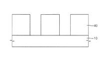
図1〜図3は、本発明の実施形態によるフォトレジストパターンの形成方法を説明するための断面図である。 1 to 3 are cross-sectional views for explaining a method of forming a photoresist pattern according to an embodiment of the present invention.
図1を参照すると、ガラス基板等のような対象物10上にアクリル系共重合体10〜35重量%と、キノンジアジド化合物5〜10重量%と、シラン系界面活性剤0.01〜0.5重量%と、ジエチレングリコール類溶媒55〜80重量%とを含む感光性樹脂組成物を塗布してフォトレジスト膜20を形成する。一例として、フォトレジスト膜20は、スピンコーティング方法によって形成することができる。具体的には、対象物10を支持する回転チャックを高速に回転させ、対象物10が回転する間、感光性樹脂組成物を対象物10上に均一に塗布してフォトレジスト膜20を形成することができる。
Referring to FIG. 1, 10 to 35% by weight of an acrylic copolymer, 5 to 10% by weight of a quinonediazide compound, and 0.01 to 0.5 of a silane surfactant on an
本発明によるフォトレジストパターンの形成方法で使用することができるアクリル系共重合体は、不飽和カルボン酸5〜40重量%と、エポキシ基含有不飽和化合物10〜70重量%と、オレフィン系不飽和化合物10〜70重量%とを共重合して得られる。アクリル系共重合体の重量平均分子量は5000〜30000である。 The acrylic copolymer that can be used in the method for forming a photoresist pattern according to the present invention comprises an unsaturated carboxylic acid of 5 to 40% by weight, an epoxy group-containing unsaturated compound of 10 to 70% by weight, and an olefinic unsaturated. It is obtained by copolymerizing 10 to 70% by weight of the compound. The weight average molecular weight of the acrylic copolymer is 5,000 to 30,000.
本発明によるフォトレジストパターンの形成方法で使用することができるシラン系界面活性剤は、下記の一般式1で示される。
フォトレジスト膜20を形成した後、フォトレジスト膜20をプリベーク(pre−bake)する段階を行って溶媒を除去する。プリベーク工程は、後続の硬化工程より低い温度で実施することが好ましい。例えば、プリベーク工程は、約80〜約110℃の温度下で1分〜15分間行うことができる。フォトレジスト膜20をプリベークすることにより、フォトレジスト膜20に含まれた有機溶媒が蒸発し、対象物10とフォトレジスト膜20の接着性が増加する。
After forming the
その後、フォトレジスト膜20の一部を除去する。以下、フォトレジスト膜20を除去する段階を具体的に説明する。
Thereafter, a part of the
図2を参照すると、マスク30を使用してフォトレジスト膜20を選択的に露光する。具体的には、露光装置のマスクステージ上に所定のパターンが形成されたマスク30を配置し、フォトレジスト膜20が形成された対象物10上にマスク30を整列させるアライン工程を行う。その後、マスク30に光を一定時間照射することにより、対象物10上に形成されたフォトレジスト膜20の所定部位がマスク30を通過した光と選択的に反応することになる。
Referring to FIG. 2, the
露光工程で使用することができる光の例としては、g線光、i線光、クリプトンフロライドレーザ、アルゴンフロライドレーザ、電子ビーム、及びX−ray等が挙げられる。 Examples of light that can be used in the exposure step include g-line light, i-line light, krypton fluoride laser, argon fluoride laser, electron beam, and X-ray.
これによって、光が照射された部位のフォトレジスト膜22は、光が照射されない部位のフォトレジスト膜20と異なるの溶解度を有することになる。
Accordingly, the
図3を参照すると、露光されたフォトレジスト膜20を現像する。即ち、現像液を利用してフォトレジスト膜20の所定部位22を除去することにより、フォトレジストパターン40を形成する。具体的には、現像液としては、アルカリ水溶液が使用される。例えば、水酸化カリウム−トリメチルアンモニウムヒドロキシド水溶液を使用することができる。現像液は、アルカリ性化合物を0.01重量%〜10重量%の濃度で超純水に溶解させて使用し、メタノール、エタノール等のような有機溶媒及び界面活性剤を適当量添加することができる。現像後、超純水で30〜90秒間洗浄して、不必要な部分を除去し乾燥してパターンを形成する。
Referring to FIG. 3, the exposed
その後、フォトレジストパターン40を硬化する段階を更に行うこともできる。硬化工程を行うことにより、フォトレジストパターン140に含まれた熱硬化性樹脂が架橋結合させることができる。硬化工程は、約150〜約250℃の温度で30〜90分間行うことが好ましい。
Thereafter, a step of curing the
その後、洗浄等の通常的な工程を経てフォトレジストパターン40を完成することができる。
Thereafter, the
本発明による感光性樹脂組成物は、流動性、コーティング安定性、感度、解像度、耐熱性、透明性、及び耐熱変色性に優れる。従って、本発明による感光性樹脂組成物でフォトレジストパターンを形成する場合、パターニングに有利である。 The photosensitive resin composition according to the present invention is excellent in fluidity, coating stability, sensitivity, resolution, heat resistance, transparency, and heat discoloration. Therefore, when forming a photoresist pattern with the photosensitive resin composition by this invention, it is advantageous to patterning.
次に、図面を参照して、本発明による感光性樹脂組成物を利用した反射−透過型液晶表示パネルを詳細に説明する。 Next, a reflection-transmission type liquid crystal display panel using the photosensitive resin composition according to the present invention will be described in detail with reference to the drawings.
〔反射−透過型液晶表示パネル〕
図4は、本発明による感光性樹脂組成物で形成したオーバーコーティング層を含む反射−透過型液晶表示パネルに対する概略的な平面図である。
[Reflective-transmissive liquid crystal display panel]
FIG. 4 is a schematic plan view of a reflection-transmission type liquid crystal display panel including an overcoating layer formed of a photosensitive resin composition according to the present invention.
図4を参照すると、反射−透過型液晶表示パネルは、表示基板100とカラーフィルタ基板200(便宜上、透過した形で示す)及び表示基板100及びカラーフィルタ基板200の間に介在される液晶層(図示せず)を含む。
Referring to FIG. 4, the reflective-transmissive liquid crystal display panel includes a
表示基板100は、表示領域DA、第1周辺領域PA1、第2周辺領域PA2、及び第3周辺領域PA3に分けられる。
The
表示領域DAには、第1方向(X軸方向)に延長された複数のゲート配線GLと、第1方向と交差する第2方向(Y軸方向)に延長された複数のソース配線DLが形成される。 In the display area DA, a plurality of gate lines GL extended in the first direction (X-axis direction) and a plurality of source lines DL extended in the second direction (Y-axis direction) intersecting the first direction are formed. Is done.
表示領域DAには、ソース配線DLとゲート配線GLによって定義される複数の画素部PXが形成され、それぞれの画素部PXは、スイッチング素子TFTとスイッチング素子TFTに電気的に連結された画素電極PEが形成される。 In the display area DA, a plurality of pixel portions PX defined by the source lines DL and the gate lines GL are formed, and each of the pixel portions PX is a pixel electrode PE electrically connected to the switching element TFT and the switching element TFT. Is formed.
画素部PXは、一部領域に反射電極が形成された反射領域RAと、反射電極が形成されない透過領域TAで構成される。透過領域TAは、反射−透過型液晶表示パネルの後面から入射された第1光(以下、内部光という)を透過し、反射領域RAは、反射−透過型液晶表示パネルの前面から入射された第2光(以下、外部光という)を反射する。 The pixel portion PX includes a reflective area RA in which a reflective electrode is formed in a partial area and a transmissive area TA in which no reflective electrode is formed. The transmissive area TA transmits first light (hereinafter referred to as internal light) incident from the rear surface of the reflective-transmissive liquid crystal display panel, and the reflective area RA is incident from the front surface of the reflective-transmissive liquid crystal display panel. Second light (hereinafter referred to as external light) is reflected.
第1周辺領域PA1には、反射−透過型液晶表示パネルに駆動信号を伝達するパッド部110が形成される。パッド部110は、フレキシブル印刷回路基板から伝達された駆動信号が印加される第1パッド部111と、駆動信号を利用してソース配線DLにデータ電圧を出力する駆動チップが実装される第2パッド部113を含む。
In the first peripheral area PA1, a
第2周辺領域PA2には、ゲート配線GLのうち、奇数番目ゲート配線にゲート信号を出力する第1ゲート回路部120が形成される。
In the second peripheral area PA2, a first
第3周辺領域PA3には、ゲート配線GLのうち、偶数番目ゲート配線にゲート信号を出力する第2ゲート回路部130が形成される。勿論、図示していないが、ゲート配線GLにゲート信号を出力するゲート回路部が第2及び第3周辺領域のうち、いずれか1つに形成することもできる。
In the third peripheral area PA3, a second
表示領域DAを取り囲む第1〜第3周辺領域PA1、PA2、PA3を含む周辺領域には、表示基板100とカラーフィルタ基板200を結合させる密封部材が形成されるシールライン領域SLが形成される。
In a peripheral region including the first to third peripheral regions PA1, PA2, and PA3 surrounding the display region DA, a seal line region SL in which a sealing member for coupling the
カラーフィルタ基板200には、画素部PXに対応するカラーフィルタパターンと、画素電極PEに対応する共通電極が形成される。カラーフィルタパターンは、例えば、レッド(R)、グリーン(G)、及びブルー(B)フィルタパターンを含む。共通電極は、液晶表示パネルの画素部PXに定義される液晶キャパシタの共通電極であって、共通電圧VCOMが印加される。
On the
液晶層(図示せず)はシールライン領域SLに密封部材が形成され、表示基板及びカラーフィルタ基板100、200を結合させた後、Y軸方向に注入される。
A liquid crystal layer (not shown) is formed with a sealing member in the seal line region SL, and after the display substrate and the
反射−透過型液晶表示パネルは、反射領域RAと透過領域TAのセルギャップを実質的に同様にするために、反射領域RAに対応して表示基板100にオーバーコーティング層を形成するか、又は、カラーフィルタ基板200にオーバーコーティング層を形成する。
In the reflective-transmissive liquid crystal display panel, an overcoating layer is formed on the
図5は、図4に示した反射−透過型液晶表示パネルに対する部分詳細平面図である。図6は、図5に示したI−I’線に沿って切断した断面図である。 FIG. 5 is a partial detailed plan view of the reflective-transmissive liquid crystal display panel shown in FIG. 6 is a cross-sectional view taken along the line I-I 'shown in FIG.
図5〜図6を参照すると、反射−透過型液晶表示パネルは、互いに隣接した第1画素部PX1と第2画素部PX2を含む。 5 to 6, the reflective-transmissive liquid crystal display panel includes a first pixel unit PX1 and a second pixel unit PX2 that are adjacent to each other.
第1画素部PX1は、互いに隣接したソース配線(DLm−1、DLm)とゲート配線(GLn−1、GLn)によって定義される。 The first pixel unit PX1 is defined by source lines (DLm-1, DLm) and gate lines (GLn-1, GLn) that are adjacent to each other.
第1画素部PX1は、表示基板100に形成された第1スイッチング素子155と第1スイッチング素子155と連結された第1画素電極157を含む。又、第1画素電極157上には第1反射電極158が形成され、第1反射電極158によって第1画素部PX1は、透過領域TAと反射領域RAに定義される。
The first pixel unit PX1 includes a
第1画素部PX1は、カラーフィルタ基板200に形成された第1カラーフィルタパターン(図示せず)を含み、第1カラーフィルタパターンによって第1画素部PX1は、所定のカラーを発現して画像を表示する。
The first pixel unit PX1 includes a first color filter pattern (not shown) formed on the
第2画素部PX2は、互いに隣接したソース配線(DLm、DLm+1)とゲート配線(GLn−1、GLn)によって定義される。 The second pixel unit PX2 is defined by source lines (DLm, DLm + 1) and gate lines (GLn-1, GLn) adjacent to each other.
第2画素部PX2は、表示基板100に形成された第2スイッチング素子165と第2スイッチング素子165と連結された第2画素電極167を含む。又、第2画素電極167上に第2反射電極168が形成され、第2反射電極168によって第2画素部PX2は、透過領域TAと反射領域RAに定義される。
The second pixel unit PX2 includes a
第2画素部PX2は、カラーフィルタ基板に形成された第2カラーフィルタパターン(図示せず)を含み、第2カラーフィルタパターンによって第2画素部PX2は、所定のカラーを発現して画像を表示する。 The second pixel unit PX2 includes a second color filter pattern (not shown) formed on the color filter substrate, and the second pixel unit PX2 develops a predetermined color and displays an image by the second color filter pattern. To do.
第1及び第2画素部P1、P2には、共通に連結されたストレージ共通配線170が形成される。ストレージ共通配線170は、ソース配線(DLm−1、DLm、DLm+1)をそれぞれカバーするように形成される。
A common
図6に示すように、反射−透過型液晶表示パネルは表示基板100と、カラーフィルタ基板200と、これらの間に介在する液晶層300を含み、反射−透過型液晶表示パネルの表示基板100は、第1ベース基板101を含む。
As shown in FIG. 6, the reflection-transmission type liquid crystal display panel includes a
第1ベース基板101上には、ゲート金属パターンにスイッチング素子155、165のゲート電極151、161、ストレージ共通配線170、及びゲート配線(GLn−1、GLn)が形成される。ストレージ共通配線170は、ソース配線(DLm−1、DLm、DLm+1)を充分にカバーできるサイズに形成することにより、ソース配線(DLm−1、DLm、DLm+1)に対応してカラーフィルタ基板200に形成される遮光パターンを形成しない場合もある。
On the
ゲート金属パターン上にはゲート絶縁層102が形成され、ゲート絶縁層102上にアモルファスシリコン層152a及びインシトゥ(in−situ)でドーピングされたn+アモルファスシリコン層152bを順次に形成してチャンネル層152を形成する。図示していないが、第2スイッチング素子のチャンネル層も形成される。
A
チャンネル層152上にソース金属パターンが形成される。ソース金属パターンは、スイッチング素子155、165のソース電極153、163、ドレイン電極154、164、及びソース配線(DLm−1、DLm、DLm+1)を含む。
A source metal pattern is formed on the
ソース金属パターン上には、表示基板の表面を平坦化するための第1オーバーコーティング層104が形成される。勿論、図示していないが、ソース金属パターン上にパッシベーション層と第1オーバーコーティング層を順次に形成することもできる。
A
第1オーバーコーティング層104は、ドレイン電極154、164の一部領域をそれぞれ露出させるコンタクトホール156、166を含む。
The
第1オーバーコーティング層104は、アクリル系共重合体10〜40重量%と、キノンジアジド化合物0.5〜25重量%と、溶媒50〜80重量%と、シラン系界面活性剤0.01〜0.5重量%とを含む感光性樹脂組成物をソース金属パターン上に塗布した後、コンタクトホールを形成することができる所定のパターンが形成されたマスクに露光及び現像して形成する。
The
アクリル系共重合体は、不飽和カルボン酸5〜40重量%と、エポキシ基含有不飽和化合物10〜70重量%と、オレフィン系不飽和化合物10〜70重量%とを共重合させて得られたアクリル系共重合体10〜40重量%を含む。アクリル系共重合体の重量平均分子量は5000〜30000である。 The acrylic copolymer was obtained by copolymerizing 5 to 40% by weight of an unsaturated carboxylic acid, 10 to 70% by weight of an epoxy group-containing unsaturated compound, and 10 to 70% by weight of an olefinic unsaturated compound. 10 to 40% by weight of acrylic copolymer is included. The weight average molecular weight of the acrylic copolymer is 5,000 to 30,000.
溶媒は、例えば、ジエチレングリコールモノメチルエーテル、ジエチレングリコールモノエチルエーテル、ジエチレングリコールジメチルエーテル、ジエチレングリコールメチルエチルエーテル、ジエチレングリコールジエチルエーテル等のジエチレングリコール類の溶媒を使用することが好ましい、 The solvent is preferably a solvent of diethylene glycols such as diethylene glycol monomethyl ether, diethylene glycol monoethyl ether, diethylene glycol dimethyl ether, diethylene glycol methyl ethyl ether, diethylene glycol diethyl ether,
シラン系界面活性剤は、下記の一般式1で示される。
感光性樹脂組成物は、流動性及びコーティング安定性に優れるので、表示基板の表面の平坦化に有利なオーバーコーティング層を形成することができる。 Since the photosensitive resin composition is excellent in fluidity and coating stability, an overcoating layer advantageous for planarization of the surface of the display substrate can be formed.
第1オーバーコーティング層104上には、画素電極157、167が形成される。一般的にそれぞれの画素電極は、1つの画素領域全体にかけて形成するか、又は、透過領域に対応して一部領域に形成することができる。画素電極は光を透過させる透明電極であって、酸化スズインジウム(ITO)、酸化亜鉛インジウム(IZO)物質等が使用される。
画素電極157、167上には反射電極158、168が形成される。反射電極158、168は、光を反射させる一種の金属パターンにアルミニウムやアルミニウム−ネオジム合金等が使用される。
ここで、第1オーバーコーティング層104の表面は、好ましく凹凸処理される。透過領域TAに対応する凹凸104aは、一種のマイクロ透過レンズの役割を果たして内部光を散乱させ、反射領域RAに対応する凹凸104aは、反射電極158、168をマイクロ反射レンズの役割を果たして外部光を散乱させる。しかし、当業者においては前記したオーバーコーティング層の表面を平坦化することもできる。
Here, the surface of the
反射−透過型液晶表示パネルのカラーフィルタ基板200は、第2ベース基板201を含む。
The
第2ベース基板201上には遮光層210が形成される。遮光層210は、一般的に表示基板100のソース配線(DLm−1、DLm、DLm+1)とゲート配線(GLn−1、GLn)に対応する領域に形成される。
A
ここでは、ソース配線の下に形成されたストレージ共通配線170がソース配線(DLm−1、DLm、DLm+1)のそれぞれを充分にカバーすることができる程度のサイズに形成することにより、遮光層210はゲート配線に対応して形成される。勿論、遮光層210は、ソース配線(DLm−1、DLm、DLm+1)に対応して形成することもできる。
Here, the storage
遮光層210が形成された第2ベース基板210上にカラーフィルタ層220を形成する。カラーフィルタ層220は、それぞれの画素部に対応して、レッド、グリーン、及びブルーフィルタパターンを含む。
A
カラーフィルタ層220上には第2オーバーコーティング層230が形成されるが、反射領域RAに対応する領域にのみ形成される。第2オーバーコーティング層230によって透過領域TAのセルギャップは、反射領域RAのセルギャップの2倍になる。即ち、第2オーバーコーティング層230によって二重セルギャップを形成する。二重セルギャップは、反射領域で反射され出射される外部光の経路長と透過領域で透過され出射される内部光の経路長を実質的に同様にする。第2オーバーコーティング層230は、第1オーバーコーティング層104と同じ感光性樹脂組成物で形成することができる。
The
第2オーバーコーティング層230上には共通電極層240が形成される。
A
次に、本発明に係る感光性樹脂組成物を利用した表示基板の製造方法を詳細に説明する。 Next, the manufacturing method of the display board | substrate using the photosensitive resin composition concerning this invention is demonstrated in detail.
〔表示基板の製造方法〕
図7〜図11は、図6に示した表示基板の製造工程を説明するための工程断面図である。
[Manufacturing method of display substrate]
7 to 11 are process cross-sectional views for explaining a manufacturing process of the display substrate shown in FIG.
図6及び図7を参照すると、第1ベース基板101上に金属層(図示せず)を形成した後、フォトリソグラフィ工程で金属層(図示せず)をエッチングして、ゲート配線GL、ゲート電極151、及びストレージ共通配線170を含むゲート金属パターンを形成する。
Referring to FIGS. 6 and 7, after a metal layer (not shown) is formed on the
金属層(図示せず)は、例えば、クロム、アルミニウム、タンタル、モリブデン、チタニウム、タングステン、銅、銀等の金属又はこれらの合金等で形成することができ、スパッタリング工程によって蒸着される。又、これら低抵抗金属層は、物理的性質が異なる2つ以上の層で形成することもできる。 The metal layer (not shown) can be formed of, for example, a metal such as chromium, aluminum, tantalum, molybdenum, titanium, tungsten, copper, silver, or an alloy thereof, and is deposited by a sputtering process. These low resistance metal layers can also be formed of two or more layers having different physical properties.
図6及び図8を参照すると、ゲート金属パターンが形成された第1ベース基板101上にプラズマ化学気相蒸着(PECVD)方法を利用して、シリコン窒化膜(SiNx)からなるゲート絶縁膜102、アモルファスシリコン層152a、及びインシトゥでドーピングされたn+アモルファスシリコン層152bを順次に形成する。その後、アモルファスシリコン層152a、及びn+アモルファスシリコン層152bをフォトエッチングして、ゲート電極151に対応する領域にチャンネル層152を形成する。
Referring to FIGS. 6 and 8, a
図6及び図9を参照すると、チャンネル層152が形成されたゲート絶縁膜102上に金属層(図示せず)を形成する。金属層(図示せず)は、例えば、クロム、アルミニウム、タンタル、モリブデン、チタニウム、タングステン、銅、銀等の金属又はこれらの合金等で形成することができ、スパッタリング工程によって蒸着される。又、これら低抵抗金属層は、物理的性質が異なる2つ以上の層で形成することもできる。
Referring to FIGS. 6 and 9, a metal layer (not shown) is formed on the
その後、金属層(図示せず)をフォトエッチングして、スイッチング素子のソース電極153、ドレイン電極154、及びソース配線DLを含むソース金属パターンを形成する。ソース電極153及びドレイン電極154は所定間隔だけ離隔して形成され、ドレイン電極は、ストレージ共通配線170の一部をカバーするように延長され形成される。
Thereafter, the metal layer (not shown) is photoetched to form a source metal pattern including the
その後、所定間隔だけ離隔したソース電極153とドレイン電極154との間に露出されたn+アモルファスシリコン層152bをエッチングしてアモルファスシリコン層152aを露出させる。
Thereafter, the n + amorphous silicon layer 152b exposed between the
図6及び図10を参照すると、ソース金属パターン上にアクリル系共重合体10〜35重量%と、キノンジアジド化合物5〜10重量%と、ジエチレングリコール類溶媒55〜80重量%と、下記の一般式1で示されるシラン系界面活性剤0.01〜0.5重量%とを含む感光性樹脂組成物を塗布する。
アクリル系共重合体は、不飽和カルボン酸5〜40重量%と、エポキシ基含有不飽和化合物10〜70重量%と、オレフィン系不飽和化合物10〜70重量%とを共重合して得られる。アクリル系共重合体の重量平均分子量は5000〜30000である。 The acrylic copolymer is obtained by copolymerizing 5 to 40% by weight of an unsaturated carboxylic acid, 10 to 70% by weight of an epoxy group-containing unsaturated compound, and 10 to 70% by weight of an olefinic unsaturated compound. The weight average molecular weight of the acrylic copolymer is 5,000 to 30,000.
溶媒は、ジエチレングリコール類の溶媒を使用する。ジエチレングリコール類の具体的な例としては、ジエチレングリコールモノメチルエーテル、ジエチレングリコールモノエチルエーテル、ジエチレングリコールジメチルエーテル、ジエチレングリコールメチルエチルエーテル、ジエチレングリコールジエチルエーテル等がある。これらは単独又は混合して使用することができる。 As the solvent, a solvent of diethylene glycol is used. Specific examples of diethylene glycols include diethylene glycol monomethyl ether, diethylene glycol monoethyl ether, diethylene glycol dimethyl ether, diethylene glycol methyl ethyl ether, and diethylene glycol diethyl ether. These can be used alone or in combination.
感光性樹脂組成物は、メラミン樹脂、接着剤、アクリル化合物等の添加剤を更に含むことができる。これらは単独又は混合して使用することができる。 The photosensitive resin composition can further contain additives such as a melamine resin, an adhesive, and an acrylic compound. These can be used alone or in combination.
添加剤の含量は、感光性樹脂組成物の総重量に対して2〜3重量%であることが好ましい。 The content of the additive is preferably 2 to 3% by weight based on the total weight of the photosensitive resin composition.
その後、所定のパターンが形成されたマスクで感光性樹脂組成物を露光及び現像してドレイン電極154の一部を露出させるコンタクトホール156を含む第1オーバーコーティング層104を形成する。感光性樹脂組成物は、流動性及びコーティング安定性に優れるので、表示基板100の表面の平坦化に有利なオーバーコーティング層を形成することができる。
Thereafter, the photosensitive resin composition is exposed and developed with a mask on which a predetermined pattern is formed to form a
好ましくは、第1オーバーコーティング層104の表面は凹凸処理される。
Preferably, the surface of the
図示していないが、第1オーバーコーティング層104の下部には、パッシベーション膜を更に形成することもできる。
Although not shown, a passivation film may be further formed below the
図11を参照すると、コンタクトホール156が形成された第1オーバーコーティング層104上に透明な導電性物質(図示せず)を形成する。透明な導電性物質は、一例としてインジウムティンオキサイド又はインジウムジンクオキサイドからなる。その後、フォトリソグラフィ工程で透明な導電性物質(図示せず)をエッチングする。これによって、コンタクトホール156を通じてドレイン電極154と電気的に接続する画素電極157が形成される。
Referring to FIG. 11, a transparent conductive material (not shown) is formed on the
その後、画素電極157上に金属層(図示せず)を形成した後、フォトリソグラフィ工程で金属層(図示せず)の一部領域を除去する。これによって、画素電極157の一部領域に反射電極158が形成される。反射電極158は、光を反射させる一種の金属パターンでアルミニウムやアルミニウム−ネオジウム合金等が使用される。反射電極158が形成された領域は反射領域RAとして定義され、反射電極158が形成されない領域は透過領域TAとして定義される。
Then, after forming a metal layer (not shown) on the
透過領域TAの凹凸104aは、一種のマイクロ透過レンズの役割を果たして内部光を散乱させ、反射領域RAに対応する凹凸104aは、反射電極158をマイクロ反射レンズの役割を果たして外部光を散乱させる。しかし、当業者においては前記した第1オーバーコーティング層の表面を平坦化することもできる。
The
図12は、図4に示した反射−透過型液晶表示パネルに対する他の実施形態による断面図である。参考として、図5に示したII−II’線に沿って切断した断面図であって、同じ構成要素には同じ符号を付与する。図5及び図12を参照すると、反射−透過型液晶表示パネルの表示基板100は第1ベース基板101を含む。
FIG. 12 is a cross-sectional view of another embodiment of the reflective-transmissive liquid crystal display panel shown in FIG. For reference, it is a cross-sectional view taken along the line II-II 'shown in FIG. 5, and the same reference numerals are given to the same components. Referring to FIGS. 5 and 12, the
第1ベース基板101上には、ゲート金属パターンにスイッチング素子155、165のゲート電極151、161、ストレージ共通配線170、及びゲート配線(GLn−1、GLn)が形成される。ストレージ共通配線170は、ソース配線(DLm−1、DLm、DLm+1)を充分にカバーできるサイズに形成されることにより、ソース配線(DLm−1、DLm、DLm+1)に対応してカラーフィルタ基板200に形成する遮光層を形成しない場合もある。
On the
ゲート金属パターン上にはゲート絶縁層102が形成され、ゲート絶縁層102上にアモルファスシリコン層162a及びインシトゥでドーピングされたn+アモルファスシリコン層162bを順次に形成してチャンネル層162を形成する。図示していないが、第1スイッチング素子155のチャンネル層も形成される。
A
チャンネル層162上にソース金属パターンが形成される。ソース金属パターンは、スイッチング素子155、165のソース電極153、163、ドレイン電極154、164、及びソース配線(DLm−1.DLm、DLm+1)を含む。
A source metal pattern is formed on the channel layer 162. The source metal pattern includes
ソース金属パターン上には、パッシベーション層103と第1オーバーコーティング層104が順次に形成される。
A
第1オーバーコーティング層104は、反射領域RAに対応する領域にのみ形成され、ドレイン電極154、164の一部領域を露出させるコンタクトホール156、166が形成される。第1オーバーコーティング層104によって透過領域TAのセルギャップは、反射領域RAのセルギャップの2倍になる。即ち、第1オーバーコーティング層104によって二重セルギャップが形成される。二重セルギャップは、反射領域RAで反射され出射される外部光の経路長と透過領域TAで透過され出射される内部光の経路長を実質的に同様にする。
The
第1オーバーコーティング層104は、アクリル系共重合体10〜40重量%と、キノンジアジド化合物0.5〜25重量%と、ジエチレングリコール類溶媒50〜80重量%と、シラン系界面活性剤0.01〜0.5重量%とを含む感光性樹脂組成物をソース金属パターン上に塗布した後、所定のパターンが形成されたマスクで露光及び現像して形成する。
The
アクリル系共重合体は、不飽和カルボン酸5〜40重量%と、エポキシ基含有不飽和化合物10〜70重量%と、オレフィン系不飽和化合物10〜70重量%とを共重合して得られたアクリル系共重合体10〜40重量%を含む。アクリル系共重合体の重量平均分子量は5000〜30000である。 The acrylic copolymer was obtained by copolymerizing 5 to 40% by weight of an unsaturated carboxylic acid, 10 to 70% by weight of an epoxy group-containing unsaturated compound, and 10 to 70% by weight of an olefinic unsaturated compound. 10 to 40% by weight of acrylic copolymer is included. The weight average molecular weight of the acrylic copolymer is 5,000 to 30,000.
ジエチレングリコール類溶媒は、例えば、ジエチレングリコールモノメチルエーテル、ジエチレングリコールモノエチルエーテル、ジエチレングリコールジメチルエーテル、ジエチレングリコールメチルエチルエーテル、ジエチレングリコールジエチルエーテル等がある。 Examples of the diethylene glycol solvent include diethylene glycol monomethyl ether, diethylene glycol monoethyl ether, diethylene glycol dimethyl ether, diethylene glycol methyl ethyl ether, and diethylene glycol diethyl ether.
シラン系界面活性剤は、下記の一般式1で表示される。
感光性樹脂組成物は、流動性及びコーティング安定性に優れるので、表示基板の表面の平坦化に有利なオーバーコーティング層を形成することができる。 Since the photosensitive resin composition is excellent in fluidity and coating stability, an overcoating layer advantageous for planarization of the surface of the display substrate can be formed.
コンタクトホール156、166が形成された第1オーバーコーティング層104上には、画素電極157、167が形成される。一般的に、それぞれの画素電極は、1つの画素領域全体にかけて形成するか、又は、透過領域に対応して一部領域に形成することができる。画素電極は光を透過させる透明導電性物質で形成され、透明導電性物質は酸化スズインジウム、酸化亜鉛インジウム物質等を含む。
画素電極157、167上には、反射電極158、168が形成される。反射電極158、168は、光を反射させる一種の金属パターンでアルミニウムやアルミニウム−ネオジム合金等が使用される。
ここで、第1オーバーコーティング層104の表面は、凹凸処理される。透過領域TAに対応する凹凸104aは、一種のマイクロ透過レンズの役割を果たして内部光を散乱させ、反射領域RAに対応する凹凸104aは、反射電極158、168をマイクロ反射レンズの役割を果たして外部光を散乱させる。しかし、当業者においては前記した第1オーバーコーティング層104の表面を平坦化することもできる。
Here, the surface of the
反射−透過型液晶表示パネルのカラーフィルタ基板200は、第2ベース基板201を含む。
The
第2ベース基板201上には、遮光層210が形成される。遮光層210は、一般的に表示基板100のソース配線(DLm−1、DLm、DLm+1)とゲート配線(GLn−1、GLn)に対応する領域に形成される。
A
ここでは、ソース配線(DLm−1、DLm、DLm+1)の下に形成されたストレージ共通配線170がソース配線(DLm−1、DLm、DLm+1)のそれぞれを充分にカバーできる程度のサイズに形成されることにより、遮光層210をゲート配線(GLn−1、GLn)にのみ対応して形成することもできる。
Here, the storage
遮光層210が形成された第2ベース基板201上にカラーフィルタ層220を形成する。カラーフィルタ層220は、第1画素部P1に形成された第1カラーフィルタパターン221と第2画素部PX2に形成された第2カラーフィルタパターン222を含む。好ましくは、カラーフィルタ層220は、レッド(R)、グリーン(G)、及びブルー(B)フィルタパターンを含む。
A
カラーフィルタ層220上には、第2オーバーコーティング層230と共通電極層240が順次に形成される。第2オーバーコーティング層230は、第1オーバーコーティング層104と同じ感光性樹脂で形成することができる。
A
次に、具体的な実施例及び比較例を挙げて本発明をより詳細に説明する。下記の例は、本発明を例示するためのもので、本発明がこれに限定されることではない。 Next, the present invention will be described in more detail with specific examples and comparative examples. The following examples are intended to illustrate the present invention, but the present invention is not limited thereto.
〔アクリル系共重合体の製造〕
(合成例1)
冷却管と攪拌器を具備したフラスコに、2,2’−アゾビス(2,4−ジメチルバレロニトリル)10重量部、及びジエチレングリコールジメチルエーテル300重量部、メタクリル酸20重量部、メタクリル酸グリシジル10重量部、2−ヒドロキシエチルアクリレート25重量部、イソボルニルアクリレート30重量部、シクロヘキシルメタクリレート15重量部を入れた後、窒素置換した後、徐々に攪拌を始めた。反応溶液を62℃まで上昇させて、この温度を5時間維持して共重合体を含む重合体溶液を得た。得られた重合体溶液の固形粉濃度は25重量%で、重合体の重量平均分子量は10000であった。ここで、重量平均分子量はゲル浸透クロマトグラフィ(Gel Permeation Chromatography;GPC)を使用して測定したポリスチレン換算平均分子量である。
[Manufacture of acrylic copolymer]
(Synthesis Example 1)
In a flask equipped with a condenser and a stirrer, 10 parts by weight of 2,2′-azobis (2,4-dimethylvaleronitrile), 300 parts by weight of diethylene glycol dimethyl ether, 20 parts by weight of methacrylic acid, 10 parts by weight of glycidyl methacrylate, After adding 25 parts by weight of 2-hydroxyethyl acrylate, 30 parts by weight of isobornyl acrylate, and 15 parts by weight of cyclohexyl methacrylate, the mixture was purged with nitrogen and then gradually stirred. The reaction solution was raised to 62 ° C., and this temperature was maintained for 5 hours to obtain a polymer solution containing a copolymer. The obtained polymer solution had a solid powder concentration of 25% by weight, and the polymer had a weight average molecular weight of 10,000. Here, a weight average molecular weight is a polystyrene conversion average molecular weight measured using gel permeation chromatography (Gel Permeation Chromatography; GPC).
〔キノンジアジド化合物の製造〕
(合成例2)
溶剤として適当量のアセトンと塩基として約2モルのトリエチルアミンの存在下で、4,4’−[1−[4−[1−[4−ヒドロキシフェニル]−1−メチルエチル]フェニル]エチリデン]ビスフェノール1molと、1,2−ナフトキノンジアジド−5−スルホン酸[クロライド]2molを縮合反応させて、[4,4’−[1−[4−[1−[4−ヒドロキシフェニル]−1−メチルエチル]フェニル]エチリデン]ビスフェノール・1,2−ナフトキノンジアジド−5−スルホン酸エステル]を得た。具体的に、縮合反応は室温で進行され、約12時間攪拌された。反応物は濾過され副産物であるトリエチルアンモニウム塩化物を除去した。アセトン溶液を水で希釈させて精製していないキノンジアジドが沈殿し、キノンジアジドはじょうごで採集し、水で洗浄された後、室温で約24時間真空乾燥した。
(Production of quinonediazide compound)
(Synthesis Example 2)
4,4 ′-[1- [4- [1- [4-hydroxyphenyl] -1-methylethyl] phenyl] ethylidene] bisphenol in the presence of a suitable amount of acetone as solvent and about 2 moles of triethylamine as base. 1 mol and 2 mol of 1,2-naphthoquinonediazide-5-sulfonic acid [chloride] were subjected to a condensation reaction to produce [4,4 ′-[1- [4- [1- [4-hydroxyphenyl] -1-methylethyl ] Phenyl] ethylidene]
〔感光性樹脂組成物の製造〕
(実施例1)
合成例1で得られた重合体溶液100重量部と、縮合物[4,4’−[1−[4−[1−[4−ヒドロキシフェニル]−1−メチルエチル]フェニル]エチリデン]ビスフェノール・1,2−ナフトキノンジアジド−5−スルホン酸エステル]8重量部とを混合して、固形粉の濃度が27重量%になるようにジエチレングリコールジメチルエーテルで溶解させ、下記の一般式2で表現される界面活性剤を全体感光性樹脂組成物に対して0.15重量%を入れた後、0.2μmのミリポアフィルタで濾過して感光性樹脂組成物を製造した。
Example 1
100 parts by weight of the polymer solution obtained in Synthesis Example 1 and the condensate [4,4 ′-[1- [4- [1- [4-hydroxyphenyl] -1-methylethyl] phenyl] ethylidene]
(実施例2)
合成例1で得られた重合体溶液100重量部と、縮合物[4,4’−[1−[4−[1−[4−ヒドロキシフェニル]−1−メチルエチル]フェニル]エチリデン]ビスフェノール・1,2−ナフトキノンジアジド−5−スルホン酸エステル]8重量部とを混合して、固形粉の濃度が27重量%になるようにジエチレングリコールメチルエチルエーテルで溶解させ、一般式2で表現される界面活性剤を全体感光性樹脂組成物に対して0.15重量%を入れた後、0.2μmのミリポアフィルタで濾過して感光性樹脂組成物を製造した。
(Example 2)
100 parts by weight of the polymer solution obtained in Synthesis Example 1 and the condensate [4,4 ′-[1- [4- [1- [4-hydroxyphenyl] -1-methylethyl] phenyl] ethylidene]
(実施例3)
合成例1で得られた重合体溶液100重量部と、縮合物[4,4’−[1−[4−[1−[4−ヒドロキシフェニル]−1−メチルエチル]フェニル]エチリデン]ビスフェノール・1,2−ナフトキノンジアジド−5−スルホン酸エステル]8重量部とを混合して、全体感光性樹脂組成物に対して固形粉の濃度が27重量%になるようにジエチレングリコールジエチルエーテルで溶解させ、一般式2で表現される界面活性剤を全体感光性樹脂組成物に対して0.15重量%を入れた後、0.2μmのミリポアフィルタで濾過して感光性樹脂組成物を製造した。
(Example 3)
100 parts by weight of the polymer solution obtained in Synthesis Example 1 and the condensate [4,4 ′-[1- [4- [1- [4-hydroxyphenyl] -1-methylethyl] phenyl] ethylidene]
(実施例4)
合成例1で得られた重合体溶液100重量部と、縮合物[4,4’−[1−[4−[1−[4−ヒドロキシフェニル]−1−メチルエチル]フェニル]エチリデン]ビスフェノール・1,2−ナフトキノンジアジド−5−スルホン酸エステル]8重量部とを混合して、固形粉の濃度が27重量%になるようにジエチレングリコールジメチルエーテルで溶解させ、下記の一般式3で表現される界面活性剤を全体感光性樹脂組成物に対して0.15重量%を入れた後、0.2μmのミリポアフィルタで濾過して感光性樹脂組成物を製造した。
100 parts by weight of the polymer solution obtained in Synthesis Example 1 and the condensate [4,4 ′-[1- [4- [1- [4-hydroxyphenyl] -1-methylethyl] phenyl] ethylidene]
(実施例5)
合成例1で得られた重合体溶液100重量部と、縮合物[4,4’−[1−[4−[1−[4−ヒドロキシフェニル]−1−メチルエチル]フェニル]エチリデン]ビスフェノール・1,2−ナフトキノンジアジド−5−スルホン酸エステル]8重量部とを混合して、固形粉の濃度が27重量%になるようにジエチレングリコールジメチルエーテルで溶解させ、下記の一般式4で表現される界面活性剤を全体感光性樹脂組成物に対して0.15重量%を入れた後、0.2μmのミリポアフィルタで濾過して感光性樹脂組成物を製造した。
100 parts by weight of the polymer solution obtained in Synthesis Example 1 and the condensate [4,4 ′-[1- [4- [1- [4-hydroxyphenyl] -1-methylethyl] phenyl] ethylidene]
(比較例1)
合成例1で得られた重合体溶液100重量部と、縮合物[4,4’−[1−[4−[1−[4−ヒドロキシフェニル]−1−メチルエチル]フェニル]エチリデン]ビスフェノール・1,2−ナフトキノンジアジド−5−スルホン酸エステル]8重量部とを混合して、固形粉の濃度が27重量%になるようにプロピレングリコールメチルエーテルアセテートで溶解させ、界面活性剤としてポリオキシエチレンオクチルフェニルエーテルを全体感光性樹脂組成物に対して0.15重量%を入れた後、0.2μmのミリポアフィルタで濾過して感光性樹脂組成物を製造した。
(Comparative Example 1)
100 parts by weight of the polymer solution obtained in Synthesis Example 1 and the condensate [4,4 ′-[1- [4- [1- [4-hydroxyphenyl] -1-methylethyl] phenyl] ethylidene]
〔実験例1−感光性樹脂組成物の流動性評価〕
上記実施例1〜実施例5及び比較例1で製造した感光性樹脂組成物の流動性を評価するための方法は次のようである。
KRUSS社のDSA−100装置のSessile Drop Methodを利用して、それぞれの感光性樹脂組成物を基板上に落とした後、それぞれの感光性樹脂組成物の基板に対する接触角を測定する。基板としては、窒化シリコン(SiNx)基板を使用した。これによる結果を下記の表1に記載した。
[Experimental example 1-fluidity evaluation of photosensitive resin composition]
The method for evaluating the fluidity of the photosensitive resin compositions produced in Examples 1 to 5 and Comparative Example 1 is as follows.
Each photosensitive resin composition is dropped on a substrate using a Sense Drop Method of a DSA-100 apparatus manufactured by KRUSS, and then the contact angle of each photosensitive resin composition to the substrate is measured. As the substrate, a silicon nitride (SiNx) substrate was used. The results are shown in Table 1 below.
表1を参照すると、本発明による実施例1、2、3、4、及び実施例5は、接触角が10°以下であり、接触角が30°以上である比較例1より流動性に優れることがわかる。 Referring to Table 1, Examples 1, 2, 3, 4 and Example 5 according to the present invention have a contact angle of 10 ° or less, and are more fluid than Comparative Example 1 having a contact angle of 30 ° or more. I understand that.
〔実験例2−感光性樹脂組成物のコーティング安定性評価〕
実施例1〜実施例5及び比較例1で製造した感光性樹脂組成物で形成したフォトレジスト膜のコーティング安定性を評価するための方法は次のようである。
まず、スピンコーターを利用して感光性樹脂組成物を下記の表2に記載したそれぞれのコーティングRPM(Revolutions Per Minute、分当り回転数)で基板上に塗布する。その後、85〜95℃で2分間プリベークしてフォトレジスト膜を形成した後、ナノスペクトロメータを利用してプリベーク温度別厚み変化を測定した。
[Experimental Example 2—Coating stability evaluation of photosensitive resin composition]
The method for evaluating the coating stability of the photoresist film formed from the photosensitive resin composition produced in Examples 1 to 5 and Comparative Example 1 is as follows.
First, a photosensitive resin composition is applied on a substrate with each coating RPM (Revolutions Per Minute, revolutions per minute) described in Table 2 below using a spin coater. Then, after prebaking at 85-95 degreeC for 2 minute (s) and forming a photoresist film, the thickness change according to prebaking temperature was measured using the nano spectrometer.
これによる結果を、下記の表2に示す。プリベーク温度が5℃変化した時の塗布膜厚みの変化が250Å以下である場合をAで表示し、厚みの変化が500Å以上である場合をBで表示した。 The results are shown in Table 2 below. The case where the change in the coating film thickness when the pre-bake temperature was changed by 5 ° C. was 250 mm or less was indicated by A, and the case where the thickness change was 500 mm or more was indicated by B.
表2を参照すると、本発明による実施例1、2、3、4、及び実施例5は厚みの変化が250Å以下であり、比較例1より厚みの変化率が低くて、コーティング安定性に優れることがわかる。 Referring to Table 2, Examples 1, 2, 3, 4 and Example 5 according to the present invention have a thickness change of 250 mm or less, a lower rate of change of thickness than Comparative Example 1, and excellent coating stability. I understand that.
〔実験例3−フォトレジストパターンの感度評価〕
実施例1〜実施例5及び比較例1で準備した感光性樹脂組成物で形成したフォトレジストパターンの感度評価のための方法は次のようである。
[Experimental Example 3-sensitivity evaluation of photoresist pattern]
The method for the sensitivity evaluation of the photoresist pattern formed with the photosensitive resin composition prepared in Examples 1 to 5 and Comparative Example 1 is as follows.
下記の表3に記載したそれぞれのコーティングRPMでそれぞれの感光性樹脂組成物を塗布した後、ホットプレート上で90℃で2分間プリベークして、3.0μm厚みのフォトレジスト膜を形成する。フォトレジスト膜に所定のパターンマスクを利用して、365nmでの強度が15mW/cm2である紫外線を15〜25秒間照射する。以後、23℃のテトラメチルアンモニウムヒドロキシド0.4重量%の水溶液で2分間現像した後、超純水で1分間洗浄してフォトレジストパターンを形成する。 Each photosensitive resin composition is applied with each coating RPM described in Table 3 below, and then pre-baked on a hot plate at 90 ° C. for 2 minutes to form a 3.0 μm-thick photoresist film. Using a predetermined pattern mask, the photoresist film is irradiated with ultraviolet rays having an intensity at 365 nm of 15 mW / cm 2 for 15 to 25 seconds. Thereafter, development is performed for 2 minutes with an aqueous solution of tetramethylammonium hydroxide at 23 ° C. at a concentration of 0.4% by weight, followed by washing with ultrapure water for 1 minute to form a photoresist pattern.
その後、フォトレジストパターンに365nmでの強度が15mW/cm2である紫外線を34秒間照射し、130℃で3分間ミッドベークした後、オーブン中で220℃で60分間硬化させる。この時、露光量は走査電子顕微鏡を利用して、8μm1:1臨界値数基準露光量とした。 Thereafter, the photoresist pattern is irradiated with ultraviolet rays having an intensity at 365 nm of 15 mW / cm 2 for 34 seconds, midbaked at 130 ° C. for 3 minutes, and then cured in an oven at 220 ° C. for 60 minutes. At this time, the exposure amount was set to 8 μm 1: 1 critical value number reference exposure amount using a scanning electron microscope.
これによる結果を下記の表3に示す。表3を参照すると、比較例1の感度が280mJ/cm2である時、実施例1、2、3、4、及び実施例5の感度は260〜270mJ/cm2であって、比較例1より高感度であることがわかる。 The results are shown in Table 3 below. Referring to Table 3, when the sensitivity of Comparative Example 1 is 280 mJ / cm 2 , the sensitivity of Examples 1, 2, 3, 4 and Example 5 is 260 to 270 mJ / cm 2. It can be seen that the sensitivity is higher.
〔実験例4−フォトレジストパターンの解像度評価〕
それぞれの感光性樹脂組成物で形成したフォトレジストパターンの解像度評価方法は次のようである。
[Experimental Example 4-Resolution Evaluation of Photoresist Pattern]
The resolution evaluation method of the photoresist pattern formed with each photosensitive resin composition is as follows.
下記の表4に記載されたそれぞれのコーティングRPMでそれぞれの感光性樹脂組成物を塗布した後、ホットプレート上で90℃で2分間プリベークして、3.0μm厚みのフォトレジスト膜を形成する。フォトレジスト膜に所定のパターンマスクを利用して365nmでの強度が15mW/cm2である紫外線を15〜25秒間照射する。その後、23℃のテトラメチルアンモニウムヒドロキシド0.4重量%の水溶液で2分間現像した後、超純水で1分間洗浄して、フォトレジストパターンを形成する。 Each photosensitive resin composition is applied with each coating RPM described in Table 4 below, and then pre-baked on a hot plate at 90 ° C. for 2 minutes to form a 3.0 μm-thick photoresist film. The photoresist film is irradiated with ultraviolet rays having an intensity at 365 nm of 15 mW / cm 2 for 15 to 25 seconds using a predetermined pattern mask. Thereafter, development is performed for 2 minutes with an aqueous solution of tetramethylammonium hydroxide of 0.4% by weight at 23 ° C., and then washed with ultrapure water for 1 minute to form a photoresist pattern.
その後、フォトレジストパターンに365nmでの強度が15mW/cm2である紫外線を34秒間照射し、130℃で3分間ミッドベークした後、オーブン中で220℃で60分間硬化させる。この時、解像度は、それぞれの感光性樹脂組成物で形成することができるフォトレジストパターンの最小サイズを測定して評価した。これによる結果を下記の表4に示す。 Thereafter, the photoresist pattern is irradiated with ultraviolet rays having an intensity at 365 nm of 15 mW / cm 2 for 34 seconds, midbaked at 130 ° C. for 3 minutes, and then cured in an oven at 220 ° C. for 60 minutes. At this time, the resolution was evaluated by measuring the minimum size of the photoresist pattern that can be formed with each photosensitive resin composition. The results are shown in Table 4 below.
表4を参照すると、実施例1〜実施例5及び比較例1を利用して形成することができるフォトレジストパターンの最小サイズは全部3μmであって、実施例1〜実施例5及び比較例1の解像度が同じ水準であることがわかる。 Referring to Table 4, the minimum size of the photoresist pattern that can be formed using Examples 1 to 5 and Comparative Example 1 is all 3 μm, and Examples 1 to 5 and Comparative Example 1 are used. It can be seen that the resolution of the same level.
〔実験例5−フォトレジストパターンの耐熱性評価〕
実施例1〜実施例5及び比較例1の感光性樹脂組成物で形成したフォトレジストパターンの耐熱性評価方法は次のようである。
[Experimental Example 5-Evaluation of heat resistance of photoresist pattern]
The heat resistance evaluation method of the photoresist pattern formed with the photosensitive resin composition of Examples 1 to 5 and Comparative Example 1 is as follows.
解像度評価方法で形成した3μmフォトレジストパターンの上下、左右の角を測定して、ミッドベーク工程前と後の各変化率を評価した。ミッドベーク工程実施前と実施後の各変化率は、実施例1及び実施例5及び比較例1で全部20%以下に同じ水準であった。 The top and bottom and left and right corners of the 3 μm photoresist pattern formed by the resolution evaluation method were measured to evaluate each change rate before and after the midbake process. The rate of change before and after the mid-baking process was the same level of 20% or less in all of Example 1, Example 5, and Comparative Example 1.
〔実験例6−フォトレジストパターンの透明性評価〕
実施例1〜実施例5及び比較例1の感光性樹脂組成物で形成したフォトレジストパターンの透明性評価方法は次のようである。
[Experimental Example 6-Transparency Evaluation of Photoresist Pattern]
The transparency evaluation method of the photoresist pattern formed with the photosensitive resin composition of Examples 1 to 5 and Comparative Example 1 is as follows.
解像度評価方法と同じ方法でフォトレジストパターンを形成した後、フォトレジストパターンに365nmでの強度が15mW/cm2である紫外線を34秒間照射し、130℃で3分間ミッドベークする。このように形成されたフォトレジストパターンに分光光度計を利用して400nm光を照射した後、透過率を測定した。透過率測定結果、実施例1〜実施例5及び比較例1の透過率は全部90%で同じ水準の透明性を示した。 After the photoresist pattern is formed by the same method as the resolution evaluation method, the photoresist pattern is irradiated with ultraviolet rays having an intensity at 365 nm of 15 mW / cm 2 for 34 seconds and then mid-baked at 130 ° C. for 3 minutes. The photoresist pattern thus formed was irradiated with 400 nm light using a spectrophotometer, and the transmittance was measured. As a result of measuring the transmittance, all the transmittances of Examples 1 to 5 and Comparative Example 1 were 90%, showing the same level of transparency.
〔実験例7−フォトレジストパターンの耐熱変色性評価〕
実施例1〜実施例5及び比較例1の感光性樹脂組成物で形成したフォトレジストパターンの耐熱変色性評価方法は次のようである。
[Experimental Example 7-Evaluation of heat discoloration of photoresist pattern]
The method for evaluating the heat discoloration resistance of photoresist patterns formed from the photosensitive resin compositions of Examples 1 to 5 and Comparative Example 1 is as follows.
透明性評価方法で形成したフォトレジストパターンを220℃のオーブンで1時間加熱した後の透過率変化で評価した。透過率変化測定結果、実施例1〜実施例5及び比較例1の透過率の変化が全部5%未満で同じ水準の耐熱変色性を有していた。 The photoresist pattern formed by the transparency evaluation method was evaluated by a change in transmittance after heating in a 220 ° C. oven for 1 hour. As a result of the transmittance change measurement, all of the transmittance changes of Examples 1 to 5 and Comparative Example 1 were less than 5% and had the same level of heat discoloration.
上述した実験例1〜実験例7からわかるように、本発明によるジエチレングリコール類の溶媒及びシラン系界面活性剤を適用した実施例1〜実施例5は、比較例1より流動性及びコーティング安定性に優れることがわかる。このことにより、本発明による感光性樹脂組成物を利用することにより、表面の平坦化性が向上されたフォトレジスト膜を形成することができる。 As can be seen from Experimental Example 1 to Experimental Example 7 described above, Examples 1 to 5 to which the solvent of diethylene glycols and the silane surfactant according to the present invention are applied are more fluid and coating stable than Comparative Example 1. It turns out that it is excellent. Thus, by using the photosensitive resin composition according to the present invention, a photoresist film with improved surface flatness can be formed.
又、実験例1〜実験例7からわかるように、本発明による感光性樹脂組成物を利用したフォトレジストパターンは、感度、解像度、耐熱性、透明性、及び耐熱変色性に優れる。従って、本発明による感光性樹脂組成物を利用してフォトレジストパターンを形成する場合、パターニングに有利である。 Further, as can be seen from Experimental Examples 1 to 7, the photoresist pattern using the photosensitive resin composition according to the present invention is excellent in sensitivity, resolution, heat resistance, transparency, and heat discoloration. Therefore, when forming a photoresist pattern using the photosensitive resin composition according to the present invention, it is advantageous for patterning.
尚、本発明は、上述の実施形態に限られるものではない。本発明の技術的範囲から逸脱しない範囲内で多様に変更実施することが可能である。 The present invention is not limited to the embodiment described above. Various modifications can be made without departing from the technical scope of the present invention.
10 対象物
20 フォトレジスト膜
30 マスク
40 フォトレジストパターン
100 表示基板
101 第1ベース基板
102 ゲート絶縁層
104 第1オーバーコーティング層
104a 凹凸
155,165 スイッチング素子
157、167 (第1、第2)画素電極
158、168 (第1、第2)反射電極
200 カラーフィルタ基板
201 第2ベース基板
210 遮光層
220 カラーフィルタ層
230 第2オーバーコーティング層
240 共通電極層
300 液晶層
DESCRIPTION OF
Claims (10)
(B)キノンジアジド(quinone diazide)化合物5〜10重量%と、
(C)溶媒55〜80重量%と、
(D)下記の一般式1で示されるシラン系界面活性剤0.01〜0.5重量%とを含むことを特徴とする感光性樹脂組成物。
(B) a quinone diazide compound of 5 to 10% by weight;
(C) 55 to 80% by weight of solvent;
(D) A photosensitive resin composition comprising 0.01 to 0.5% by weight of a silane surfactant represented by the following general formula 1.
Applications Claiming Priority (2)
| Application Number | Priority Date | Filing Date | Title |
|---|---|---|---|
| KR10-2005-0117111 | 2005-12-02 | ||
| KR1020050117111A KR101288411B1 (en) | 2005-12-02 | 2005-12-02 | Photosensitive resin composition, method for forming a photoresist pattern and method for manufacturing a display substrate using the same |
Publications (3)
| Publication Number | Publication Date |
|---|---|
| JP2007156471A JP2007156471A (en) | 2007-06-21 |
| JP2007156471A5 JP2007156471A5 (en) | 2009-11-12 |
| JP4817188B2 true JP4817188B2 (en) | 2011-11-16 |
Family
ID=38119167
Family Applications (1)
| Application Number | Title | Priority Date | Filing Date |
|---|---|---|---|
| JP2006324270A Expired - Fee Related JP4817188B2 (en) | 2005-12-02 | 2006-11-30 | Photosensitive resin composition |
Country Status (3)
| Country | Link |
|---|---|
| US (1) | US7371499B2 (en) |
| JP (1) | JP4817188B2 (en) |
| KR (1) | KR101288411B1 (en) |
Cited By (1)
| Publication number | Priority date | Publication date | Assignee | Title |
|---|---|---|---|---|
| JP2014164305A (en) * | 2013-02-27 | 2014-09-08 | Samsung Display Co Ltd | Photosensitive resin product, and display device using the same |
Families Citing this family (13)
| Publication number | Priority date | Publication date | Assignee | Title |
|---|---|---|---|---|
| KR100701641B1 (en) * | 2004-08-02 | 2007-03-30 | 도레이새한 주식회사 | Method and apparatus for manufacturing flexible printed circuit board depositing copper plating layer by vapor deposition |
| JP4849251B2 (en) * | 2007-01-18 | 2012-01-11 | Jsr株式会社 | Radiation-sensitive resin composition, interlayer insulating film and microlens, and production method thereof |
| JP4352085B2 (en) | 2007-12-18 | 2009-10-28 | 株式会社東芝 | Information processing apparatus and cutting control method |
| KR101378439B1 (en) * | 2008-08-20 | 2014-03-28 | 삼성디스플레이 주식회사 | Organic light emitting diode display and method for manufacturing the same |
| KR101669085B1 (en) * | 2009-01-28 | 2016-10-25 | 제이에스알 가부시끼가이샤 | Radiation sensitive resin composition, and interlayer insulating film and forming method thereof |
| KR101290057B1 (en) * | 2010-07-19 | 2013-07-26 | 주식회사 엘지화학 | Thermally curable resin composition with good coating and recoating property |
| KR101229960B1 (en) * | 2011-01-28 | 2013-02-06 | 한양대학교 산학협력단 | Photoacid generator bound tetra-polymer resist and the synthesis of the same |
| JP5727350B2 (en) * | 2011-10-26 | 2015-06-03 | 信越化学工業株式会社 | Method for producing resist composition for lithography, method for producing resist protective film forming composition, method for producing silicon-containing resist underlayer film forming method, and method for producing organic resist underlayer film forming composition |
| KR102025099B1 (en) * | 2011-12-13 | 2019-09-25 | 주식회사 동진쎄미켐 | Photoresist composition |
| US9772558B2 (en) | 2013-09-24 | 2017-09-26 | International Business Machines Corporation | Sulfonic acid ester containing polymers for organic solvent based dual-tone photoresists |
| KR102059225B1 (en) | 2015-11-27 | 2019-12-26 | 주식회사 엘지화학 | Curable composition and method for manufacturing pattern using the same |
| CN109422987B (en) * | 2017-08-30 | 2021-03-09 | 京东方科技集团股份有限公司 | Composition for planarization layer, preparation method thereof, planarization layer material and display device |
| JP7056320B2 (en) * | 2018-03-30 | 2022-04-19 | 住友ベークライト株式会社 | Photosensitive resin composition, resin film and electronic device |
Family Cites Families (10)
| Publication number | Priority date | Publication date | Assignee | Title |
|---|---|---|---|---|
| JPS63250311A (en) * | 1987-04-06 | 1988-10-18 | Kao Corp | Water-in-oil type cosmetic |
| JPH07281018A (en) * | 1994-04-06 | 1995-10-27 | Sumitomo Chem Co Ltd | Positive type resist composition |
| DE60137398D1 (en) * | 2000-11-30 | 2009-03-05 | Fujifilm Corp | Lithographic printing plate precursors |
| JP2003215800A (en) | 2002-01-24 | 2003-07-30 | Kodak Polychrome Graphics Japan Ltd | Photosensitive composition and photosensitive lithographic printing plate |
| KR100973799B1 (en) * | 2003-01-03 | 2010-08-03 | 삼성전자주식회사 | Photoresist composition for multi-micro nozzle head coater |
| JP4315013B2 (en) | 2003-08-01 | 2009-08-19 | Jsr株式会社 | Radiation-sensitive resin composition, interlayer insulating film and microlens, and production method thereof |
| KR20050022494A (en) * | 2003-09-02 | 2005-03-08 | 삼성전자주식회사 | Photoresist Composition of Liquid Crystal Display Device for Spinless Coater and Method of Forming A Photoresist Pattern Using the Same |
| JP4586703B2 (en) * | 2004-10-14 | 2010-11-24 | 住友化学株式会社 | Radiation sensitive resin composition |
| KR101112545B1 (en) * | 2004-12-16 | 2012-03-13 | 스미또모 가가꾸 가부시끼가이샤 | Photosensitive resin and thin film panel comprising pattern made of the photosensitive resin and method for manufacturing the thin film panel |
| KR101209049B1 (en) * | 2004-12-24 | 2012-12-07 | 스미또모 가가꾸 가부시끼가이샤 | Photosensitive resin and thin film panel comprising pattern made of the photosensitive resin and method for manufacturing the thin film panel |
-
2005
- 2005-12-02 KR KR1020050117111A patent/KR101288411B1/en not_active IP Right Cessation
-
2006
- 2006-10-19 US US11/550,897 patent/US7371499B2/en active Active
- 2006-11-30 JP JP2006324270A patent/JP4817188B2/en not_active Expired - Fee Related
Cited By (1)
| Publication number | Priority date | Publication date | Assignee | Title |
|---|---|---|---|---|
| JP2014164305A (en) * | 2013-02-27 | 2014-09-08 | Samsung Display Co Ltd | Photosensitive resin product, and display device using the same |
Also Published As
| Publication number | Publication date |
|---|---|
| JP2007156471A (en) | 2007-06-21 |
| US7371499B2 (en) | 2008-05-13 |
| US20070128540A1 (en) | 2007-06-07 |
| KR20070057540A (en) | 2007-06-07 |
| KR101288411B1 (en) | 2013-07-22 |
Similar Documents
| Publication | Publication Date | Title |
|---|---|---|
| JP4817188B2 (en) | Photosensitive resin composition | |
| KR101302508B1 (en) | Negative photosensitive resin composition, liquid crystal display having that curing product, method of forming a pattern of liquid crystal display using the same | |
| JP5031271B2 (en) | Method for manufacturing common electrode substrate | |
| CN116068853A (en) | Photosensitive resin composition and display device | |
| CN104937491B (en) | Photosensitive resin composition and method for forming pattern using the same | |
| JP4516150B1 (en) | Photosensitive resin composition | |
| KR101482552B1 (en) | Negative photosensitive resin composition | |
| CN104007616B (en) | Photosensitive resin composition and display device using the same | |
| KR101326595B1 (en) | Photosensitive resin composition and method of manufacturing a thin film transistor substrate and method of manufacturing a common electrode substrate using the same | |
| KR101388519B1 (en) | Method Of Fabricating Thin Film Transistor Substrate And Photosensitive Resin Composition Used To The Same | |
| KR102247811B1 (en) | Photoresist composition and method for manufacturing a thin film transistor substrate using the same | |
| KR100922844B1 (en) | Photosensitive resin composition for dielectrics | |
| KR20070038902A (en) | Curable resin composition, process for forming a cured film, and cured film | |
| JP5157860B2 (en) | Radiation-sensitive resin composition, interlayer insulating film and microlens, and production method thereof | |
| KR20140131609A (en) | Photosensitive resin composition, method of forming pattern, and liquid crystal display using the same | |
| KR20100063540A (en) | Negative photosensitive resin composition | |
| TW201439675A (en) | Photosensitive resin composition | |
| JP2008165127A (en) | Photosensitive resin composition | |
| KR100922843B1 (en) | Photosensitive resin composition for dielectrics | |
| KR20190128559A (en) | Wiring member and method for manufacturing the wiring member | |
| KR102233412B1 (en) | Photosensitive resin composition and method of forming pattern using the same | |
| JP6093438B2 (en) | Photosensitive resin composition, method for producing cured film, cured film, organic EL display device and liquid crystal display device | |
| JP2020079937A (en) | Positive photosensitive resin composition | |
| KR20060086020A (en) | Photosensitive resin and thin film panel comprising patterns made of the photosensitive resin and method for manufacturing the thin film panel |
Legal Events
| Date | Code | Title | Description |
|---|---|---|---|
| A521 | Request for written amendment filed |
Free format text: JAPANESE INTERMEDIATE CODE: A523 Effective date: 20090925 |
|
| A621 | Written request for application examination |
Free format text: JAPANESE INTERMEDIATE CODE: A621 Effective date: 20090925 |
|
| A521 | Request for written amendment filed |
Free format text: JAPANESE INTERMEDIATE CODE: A523 Effective date: 20100917 |
|
| A977 | Report on retrieval |
Free format text: JAPANESE INTERMEDIATE CODE: A971007 Effective date: 20110712 |
|
| TRDD | Decision of grant or rejection written | ||
| A01 | Written decision to grant a patent or to grant a registration (utility model) |
Free format text: JAPANESE INTERMEDIATE CODE: A01 Effective date: 20110726 |
|
| A01 | Written decision to grant a patent or to grant a registration (utility model) |
Free format text: JAPANESE INTERMEDIATE CODE: A01 |
|
| A61 | First payment of annual fees (during grant procedure) |
Free format text: JAPANESE INTERMEDIATE CODE: A61 Effective date: 20110823 |
|
| FPAY | Renewal fee payment (event date is renewal date of database) |
Free format text: PAYMENT UNTIL: 20140909 Year of fee payment: 3 |
|
| R150 | Certificate of patent or registration of utility model |
Ref document number: 4817188 Country of ref document: JP Free format text: JAPANESE INTERMEDIATE CODE: R150 Free format text: JAPANESE INTERMEDIATE CODE: R150 |
|
| FPAY | Renewal fee payment (event date is renewal date of database) |
Free format text: PAYMENT UNTIL: 20140909 Year of fee payment: 3 |
|
| S111 | Request for change of ownership or part of ownership |
Free format text: JAPANESE INTERMEDIATE CODE: R313111 |
|
| FPAY | Renewal fee payment (event date is renewal date of database) |
Free format text: PAYMENT UNTIL: 20140909 Year of fee payment: 3 |
|
| R350 | Written notification of registration of transfer |
Free format text: JAPANESE INTERMEDIATE CODE: R350 |
|
| R250 | Receipt of annual fees |
Free format text: JAPANESE INTERMEDIATE CODE: R250 |
|
| R250 | Receipt of annual fees |
Free format text: JAPANESE INTERMEDIATE CODE: R250 |
|
| R250 | Receipt of annual fees |
Free format text: JAPANESE INTERMEDIATE CODE: R250 |
|
| R250 | Receipt of annual fees |
Free format text: JAPANESE INTERMEDIATE CODE: R250 |
|
| R250 | Receipt of annual fees |
Free format text: JAPANESE INTERMEDIATE CODE: R250 |
|
| R250 | Receipt of annual fees |
Free format text: JAPANESE INTERMEDIATE CODE: R250 |
|
| R250 | Receipt of annual fees |
Free format text: JAPANESE INTERMEDIATE CODE: R250 |
|
| LAPS | Cancellation because of no payment of annual fees |