JP4788552B2 - LIGHT EMITTING DEVICE, ELECTRONIC DEVICE, AND METHOD FOR MANUFACTURING LIGHT EMITTING DEVICE - Google Patents
LIGHT EMITTING DEVICE, ELECTRONIC DEVICE, AND METHOD FOR MANUFACTURING LIGHT EMITTING DEVICE Download PDFInfo
- Publication number
- JP4788552B2 JP4788552B2 JP2006267598A JP2006267598A JP4788552B2 JP 4788552 B2 JP4788552 B2 JP 4788552B2 JP 2006267598 A JP2006267598 A JP 2006267598A JP 2006267598 A JP2006267598 A JP 2006267598A JP 4788552 B2 JP4788552 B2 JP 4788552B2
- Authority
- JP
- Japan
- Prior art keywords
- region
- light emitting
- bank
- liquid repellent
- pixel electrode
- Prior art date
- Legal status (The legal status is an assumption and is not a legal conclusion. Google has not performed a legal analysis and makes no representation as to the accuracy of the status listed.)
- Expired - Fee Related
Links
Images


Landscapes
- Electroluminescent Light Sources (AREA)
Description
本発明は、発光層を有する発光装置、電子機器、及び発光装置の製造方法に関する。 The present invention relates to a light emitting device having a light emitting layer, an electronic apparatus, and a method for manufacturing the light emitting device.
上記発光装置の一つに、発光層に有機発光材料を用いた有機EL(Electro Luminescence)装置がある。有機EL装置の製造方法としては、いわゆる液滴吐出法を用いた方法が知られている。これは、基板上に各画素(発光領域)を囲うようにして形成されたバンク(隔壁)の作る凹部に、有機発光材料が溶解又は分散された機能液を吐出し、これを乾燥させることによって発光層を形成するものである(特許文献1参照)。 One of the light emitting devices is an organic EL (Electro Luminescence) device using an organic light emitting material for a light emitting layer. As a method for manufacturing an organic EL device, a method using a so-called droplet discharge method is known. This is because a functional liquid in which an organic light emitting material is dissolved or dispersed is discharged into a concave portion formed by a bank (partition) formed so as to surround each pixel (light emitting region) on the substrate and dried. A light emitting layer is formed (see Patent Document 1).
しかしながら、液滴吐出法によって形成された発光層には、厚さが不均一になりやすいという問題点がある。すなわち、バンクの撥液性や高さ、機能液の体積、乾燥の速さ等のパラメータに依存して、発光層が凹部内に凹状を呈して形成されたり、凸状を呈して形成されたりする場合がある。こうした発光層の厚さの不均一により、発光装置の発光特性にばらつきが生じてしまう。 However, the light emitting layer formed by the droplet discharge method has a problem that the thickness tends to be non-uniform. That is, depending on parameters such as the liquid repellency and height of the bank, the volume of the functional liquid, and the drying speed, the light emitting layer may be formed with a concave shape in the concave portion, or may be formed with a convex shape. There is a case. Such uneven thickness of the light emitting layer causes variations in the light emission characteristics of the light emitting device.
本発明は、以上の問題点に鑑みてなされたものであり、本発明の奏する効果の一つにより、発光領域において発光層の厚さを均一にすることが可能となる。 The present invention has been made in view of the above problems, and the thickness of the light emitting layer in the light emitting region can be made uniform in one of the effects exhibited by the present invention.
本発明の発光装置は、複数の発光領域を有する発光装置であって、基板と、前記基板上に、前記発光領域ごとに形成された画素電極と、前記基板上のうち、前記発光領域を除いた領域に形成され、かつ前記基板の法線方向から見て一部が前記画素電極の外縁部に重なった状態に形成された第1バンクと、前記第1バンク上に形成され、前記発光領域を囲む環状の第1撥液領域、前記第1撥液領域を囲む環状の親液領域、及び前記親液領域の外側に配置された第2撥液領域を有する第2バンクと、前記画素電極上のうち、前記第1撥液領域に囲まれた領域に配置された正孔注入層と、前記正孔注入層上及び前記第2バンク上のうち、前記第2撥液領域に囲まれた領域に配置された発光層と、前記発光層を挟んで前記画素電極の反対側に形成された陰極と、を備え、前記第2バンクにおける前記親液領域は、前記第1撥液領域及び前記第2撥液領域より濡れ性が高いことを特徴とする。 The light-emitting device of the present invention is a light-emitting device having a plurality of light-emitting regions, except for a substrate, a pixel electrode formed for each of the light-emitting regions on the substrate, and the light-emitting region out of the substrate. A first bank formed on the first bank and formed on the first bank so as to partially overlap the outer edge of the pixel electrode when viewed from the normal direction of the substrate; A second bank having an annular first lyophobic region surrounding the first lyophilic region, an annular lyophilic region surrounding the first lyophobic region, and a second lyophobic region disposed outside the lyophilic region; Among the above, the hole injection layer disposed in a region surrounded by the first liquid repellent region, and the second liquid repellent region among the hole injection layer and the second bank are surrounded by the second liquid repellent region Formed on the opposite side of the pixel electrode across the light emitting layer. Comprising a cathode, said lyophilic area in the second bank, characterized by a high wettability than the first liquid repellent area and the second liquid repellent area.
このような構成によれば、発光領域の周囲は第1撥液領域に囲まれているため、正孔注入層を形成する際に吐出される機能液は発光領域外には浸入しにくい。このため、正孔注入層を容易に発光領域内に形成することができる。また、第2撥液領域の存在により、発光層を形成する際に吐出される機能液は、親液領域及びその内側の領域にのみ濡れ広がり、第2撥液領域には侵入しにくい。このため、発光層を容易に第2撥液領域に囲まれた領域に形成することができる。こうして形成された発光層は、正孔注入層の面積(すなわち発光領域の面積)より大きな面積を有しているため、発光層のうち比較的平坦な領域を発光に用いることができる。したがって、上記構成によれば、均一な発光特性を有する発光装置が得られる。 According to such a configuration, since the periphery of the light emitting region is surrounded by the first liquid repellent region, the functional liquid discharged when forming the hole injection layer is difficult to enter the light emitting region. For this reason, the hole injection layer can be easily formed in the light emitting region. Further, due to the presence of the second liquid repellent area, the functional liquid discharged when forming the light emitting layer wets and spreads only in the lyophilic area and the inner area, and hardly enters the second liquid repellent area. For this reason, the light emitting layer can be easily formed in a region surrounded by the second liquid repellent region. Since the light emitting layer thus formed has an area larger than the area of the hole injection layer (that is, the area of the light emitting region), a relatively flat region of the light emitting layer can be used for light emission. Therefore, according to the above configuration, a light emitting device having uniform light emission characteristics can be obtained.
本発明の電子機器は、上記発光装置を備えることを特徴とする。このような構成によれば、均一な発光特性を有する電子機器が得られる。 An electronic apparatus according to the present invention includes the light emitting device. According to such a configuration, an electronic device having uniform light emission characteristics can be obtained.
本発明の発光装置の製造方法は、複数の発光領域を有する発光装置の製造方法であって、基板上に、前記発光領域ごとに画素電極を形成するステップと、前記基板上に、前記画素電極を覆って、第1バンク材料、濡れ性可変バンク材料をこの順に積層させた後に、前記第1バンク材料及び前記濡れ性可変バンク材料のうち前記発光領域に対応する領域に開口部を形成することにより、第1バンク及び濡れ性可変バンクを形成するステップと、前記濡れ性可変バンクの表面の領域であって、前記発光領域を囲む環状の領域A、前記領域Aを囲む環状の領域B、前記領域Bの外側の領域Cのうち、前記領域Bにエネルギーを照射することにより、前記領域Aに第1撥液領域を、前記領域Bに前記第1撥液領域より濡れ性の高い親液領域を、前記領域Cに前記親液領域より濡れ性の低い第2撥液領域をそれぞれ形成して、前記第1撥液領域、前記親液領域、前記第2撥液領域を有する第2バンクを形成するステップDと、前記画素電極上のうち、前記第1撥液領域に囲まれた領域に、液滴吐出法により正孔注入層を形成するステップと、前記正孔注入層上及び前記第2バンク上のうち、前記第2撥液領域に囲まれた領域に、液滴吐出法により発光層を形成するステップと、前記発光層を挟んで前記画素電極の反対側に陰極を形成するステップと、を備えることを特徴とする。 The method for manufacturing a light emitting device according to the present invention is a method for manufacturing a light emitting device having a plurality of light emitting regions, the step of forming a pixel electrode for each light emitting region on a substrate, and the pixel electrode on the substrate. The first bank material and the wettability variable bank material are stacked in this order, and then an opening is formed in a region corresponding to the light emitting region of the first bank material and the wettability variable bank material. A step of forming the first bank and the wettability variable bank, and a region on the surface of the wettability variable bank, the annular region A surrounding the light emitting region, the annular region B surrounding the region A, Of the region C outside the region B, by irradiating the region B with energy, the region A has a first liquid repellent region, and the region B has a higher lyophilic region than the first liquid repellent region. The territory Forming a second liquid repellent area having lower wettability than the lyophilic area in C to form a second bank having the first lyophobic area, the lyophilic area, and the second lyophobic area; A step of forming a hole injection layer by a droplet discharge method in a region surrounded by the first liquid repellent region on the pixel electrode, and on the hole injection layer and the second bank A step of forming a light emitting layer in a region surrounded by the second liquid repellent region by a droplet discharge method, and a step of forming a cathode on the opposite side of the pixel electrode with the light emitting layer interposed therebetween. It is characterized by that.
また、上記発光装置の製造方法において、前記ステップDは、前記領域A及び前記領域Cを遮光して前記領域Bに紫外線を照射するステップを含むことが好ましい。 In the method for manufacturing a light emitting device, the step D preferably includes a step of shielding the region A and the region C and irradiating the region B with ultraviolet rays.
このような製造方法によれば、ステップDにおいて、発光領域の周囲に第1撥液領域が形成される。このため、正孔注入層を形成するステップにおいて液滴吐出法により吐出された機能液は、発光領域外に浸入しにくいので、正孔注入層を容易に発光領域内に形成することができる。また、ステップDにおいて形成された第2撥液領域の存在により、発光層を形成するステップにおいて液滴吐出法により吐出された機能液は、親液領域及びその内側の領域にのみ濡れ広がり、第2撥液領域には侵入しにくい。このため、発光層を容易に第2撥液領域に囲まれた領域に形成することができる。こうして形成された発光層は、正孔注入層(又は発光領域)より大きな面積を有しているため、発光層のうち比較的平坦な領域を発光に用いることができる。したがって、上記製造方法によれば、簡便な製造プロセスで、均一な発光特性を有する発光装置が得られる。 According to such a manufacturing method, in Step D, the first liquid repellent region is formed around the light emitting region. For this reason, since the functional liquid discharged by the droplet discharge method in the step of forming the hole injection layer is difficult to enter the light emitting region, the hole injection layer can be easily formed in the light emitting region. Further, due to the presence of the second liquid repellent region formed in Step D, the functional liquid discharged by the droplet discharge method in the step of forming the light emitting layer wets and spreads only in the lyophilic region and the inner region, and 2 It is difficult to enter the liquid repellent area. For this reason, the light emitting layer can be easily formed in a region surrounded by the second liquid repellent region. Since the light emitting layer thus formed has a larger area than the hole injection layer (or light emitting region), a relatively flat region of the light emitting layer can be used for light emission. Therefore, according to the manufacturing method, a light emitting device having uniform light emission characteristics can be obtained with a simple manufacturing process.
また、第2バンクにおける第1撥液領域、親液領域、第2撥液領域を利用することにより、凹凸の少ない平坦な面で発光層のパターニングを行うことができる。これにより、発光層が形成された状態における基板の表面(すなわち陰極の形成領域)が平坦な状態となるため、陰極を高品位に形成することができる。 In addition, by using the first liquid repellent region, the lyophilic region, and the second liquid repellent region in the second bank, the light emitting layer can be patterned on a flat surface with few irregularities. As a result, the surface of the substrate (that is, the cathode formation region) in a state where the light emitting layer is formed becomes flat, so that the cathode can be formed with high quality.
ここで、上記液滴吐出法とは、有機発光材料等の機能物質が溶解又は分散された機能液の液滴を吐出し、その後、吐出された機能液を乾燥させて溶媒を蒸発させ、機能物質の層を形成する手法である。液滴吐出法には、インクジェット法やディスペンサ塗布法などが含まれる。 Here, the droplet discharge method is a method of discharging functional liquid droplets in which a functional substance such as an organic light emitting material is dissolved or dispersed, and then drying the discharged functional liquid to evaporate the solvent. This is a method of forming a layer of material. The droplet discharge method includes an inkjet method and a dispenser coating method.
以下、図面を参照し、本発明の実施形態について説明する。なお、以下に示す各図においては、各構成要素を図面上で認識され得る程度の大きさとするため、各構成要素の寸法や比率を実際のものとは適宜に異ならせてある。 Hereinafter, embodiments of the present invention will be described with reference to the drawings. In the drawings shown below, the dimensions and ratios of the components are appropriately different from the actual ones in order to make the components large enough to be recognized on the drawings.
(発光装置)
図1は、本発明の発光装置としての有機EL装置1の平面図である。有機EL装置1は、透光性を有する矩形のガラス基板10を基体として構成されており、ガラス基板10には、複数の円形の発光領域5が設けられている。発光領域5は、ガラス基板10の長手方向に沿って列をなすように等間隔に形成されている。そして、この発光領域5の列は、ガラス基板10上に2列に配列されている。また、各発光領域5は、隣接する他方の列の発光領域5に対してガラス基板10の長手方向について半ピッチだけずれるようにして配置されている。つまり、発光領域5は、千鳥状に配列されている。有機EL装置1は、発光領域5において発光を行う。図1は、有機EL装置1を、光が射出される側から見た図である。ここで、ガラス基板10は、本発明における基板に対応する。基板としては、ガラス基板10の他にも、石英基板を始めとする種々の部材を用いることができる。
(Light emitting device)
FIG. 1 is a plan view of an
図2は、図1中の発光領域5の周辺部分の拡大図であり、図3は、図2中のE−E線における有機EL装置1の断面図である。以下では、図3の断面図を用いて、図2の平面図を参照しながら有機EL装置1の構造について説明する。
2 is an enlarged view of a peripheral portion of the
有機EL装置1は、ガラス基板10を基体とし、その上に各構成要素が積み上げられた構成となっている。ガラス基板10上にはシリコン酸化膜(SiO2)等からなる下地保護膜31が形成されている。下地保護膜31上には、TFT(Thin Film Transistor)素子27が形成されている。
The
より詳しくは、下地保護膜31上に、ポリシリコン膜からなる半導体膜21が島状に形成されている。半導体膜21には不純物の導入によってソース領域、ドレイン領域が形成され、不純物が導入されなかった部分がチャネル領域となっている。下地保護膜31及び半導体膜21の上には、シリコン酸化膜等からなるゲート絶縁膜32が形成され、ゲート絶縁膜32上には、アルミニウム(Al)、モリブデン(Mo)、タンタル(Ta)、チタン(Ti)、タングステン(W)等からなるゲート電極23が形成されている。ゲート電極23及びゲート絶縁膜32の上には、第1層間絶縁膜33と第2層間絶縁膜34とがこの順に積層されている。ここで、第1層間絶縁膜33及び第2層間絶縁膜34は、シリコン酸化膜(SiO2)、チタン酸化膜(TiO2)などの無機絶縁膜から構成されている。なお、下地保護膜31から第2層間絶縁膜34までの構成要素を、以下ではまとめて「回路素子層19」とも呼ぶ。
More specifically, the
第1層間絶縁膜33の上層には、共通給電線25が形成されている。共通給電線25は、第1層間絶縁膜33及びゲート絶縁膜32を貫通して設けられたコンタクトホールを介して半導体膜21のソース領域に接続されている。
A common
第2層間絶縁膜34上には、ITO(Indium Tin Oxide)からなる光透過性の画素電極11が発光領域5ごとに形成されている。画素電極11は、図1の平面図において、発光領域5として示された円より一回り大きな領域に形成されている。また、発光領域5は、ガラス基板10の長手方向に沿って列をなすように等間隔に形成されている。この画素電極11は、第2層間絶縁膜34、第1層間絶縁膜33、ゲート絶縁膜32を貫通して設けられたコンタクトホールを介して半導体膜21のドレイン領域に電気的に接続されている。こうした構成において、TFT素子27は、ゲート電極23への電圧の供給によってオン/オフが切り替わり、オン状態となった場合には、共通給電線25から画素電極11へ駆動電流を流す働きをする。
A light-
また、第2層間絶縁膜34上には、無機材料からなる第1バンク12が形成されている。第1バンク12は、画素電極11の周りを囲うようにして第2層間絶縁膜34上に配置されており、ガラス基板10の法線方向から見て、一部が画素電極11の外縁部に重なった状態に形成されている。換言すれば、第1バンク12は、画素電極11より小さな開口部12aを有して、画素電極11に重ねて配置されている。そして、この開口部12aは、発光領域5に対応する領域に設けられている。つまり、図1に示された発光領域5の形状が、そのまま開口部12aの形状となる。言い換えれば、第1バンク12は、発光領域5を除いた領域に形成されていることとなる。第1バンク12は、シリコン酸化膜等の無機絶縁膜からなり、その厚さは約50〜100nmである。
A
第1バンク12の上には、第1バンク12と同一の形成領域に、第2バンク22が積層されている。第2バンク22は、第1撥液領域22a、親液領域22b、第2撥液領域22cを有している。第1撥液領域22aは、図1及び図2に示された、発光領域5を囲む環状の領域Aに形成されている。親液領域22bは、領域Aを囲む環状の領域Bに形成されている。第2撥液領域22cは、領域Bの外側に対応する領域Cに形成されている。本実施形態では、領域A及び領域Bは、ともに同心の円環状の領域となっている。また、領域Aの内円が発光領域5に一致し、領域Aの外円と領域Bの内円とが一致している。したがって、発光領域5、第1撥液領域22aが形成された領域A、親液領域22bが形成された領域B、第2撥液領域22cが形成された領域Cは、隣り合う領域同士が接した状態で配置されており、ガラス基板10の法線方向から見ると、有機EL装置1上の領域は、発光領域5、領域A、領域B、領域Cのいずれかに含まれる。本実施形態では、発光領域5の円の直径は約50μm、第1撥液領域22aが形成された領域Aの幅は約5μm、親液領域22bが形成された領域Bの幅は約20μmである。
A
ここで、第2バンク22における親液領域22bは、第1撥液領域22a及び第2撥液領域22cより相対的に濡れ性が高くなっている。本明細書で相対的に「濡れ性が高い」とは、液体との接触角が相対的に小さいことを指す。ある領域に吐出された液体は、これと隣接する、相対的に濡れ性が低い(すなわち接触角が大きい)領域には浸入しにくいと言える。したがって、本実施形態では、発光領域5に吐出された液体は第1撥液領域22aには侵入しにくく、親液領域22bに吐出された液体は、第2撥液領域22cには浸入しにくくなっている。第2バンク22の詳細な材料及び製造方法については後述する。
Here, the
画素電極11上のうち、第1撥液領域22aに囲まれた領域、すなわち発光領域5に対応する領域には、正孔注入層14が形成されている。より詳しくは、正孔注入層14は、画素電極11を底部とし、第1バンク12及び第2バンク22を側壁とする凹部に形成されている。正孔注入層14が形成される発光領域5は、周囲を第2バンク22の第1撥液領域22aに囲まれているため、正孔注入層14を形成する際に吐出される機能液は発光領域5の外に浸入しにくい。このため、正孔注入層14を容易に発光領域5内に形成することができる。
On the
正孔注入層14は、導電性高分子材料中にドーパントを含有する導電性高分子層からなる。このような正孔注入層14は、例えば、ドーパントとしてポリスチレンスルホン酸を含有する3,4−ポリエチレンジオキシチオフェン(PEDOT−PSS)などから構成することができる。
The
正孔注入層14上及び第2バンク22上のうち、第2撥液領域22cに囲まれた領域(すなわち、発光領域5、第1撥液領域22a、親液領域22bからなる領域)には、発光層15が形成されている。第2撥液領域22cの存在により、発光層15を形成する際に吐出される機能液は、親液領域22b及びその内側の領域にのみ濡れ広がり、第2撥液領域22cには侵入しにくい。このため、発光層15を容易に第2撥液領域22cに囲まれた領域に形成することができる。こうして形成された発光層15は、正孔注入層14の面積(すなわち発光領域5の面積)より大きな面積を有しているため、発光領域5において、発光層15の厚さを均一にすることができる。すなわち、発光層15のうち比較的平坦な領域を発光に用いることができる。
Of the region on the
本明細書では、正孔注入層14、発光層15を含む層を有機EL素子3とも呼ぶ。正孔注入層14の厚さは約50nmであり、発光層15の厚さは約100nmである。
In this specification, the layer including the
発光層15上及び第2バンク22の第2撥液領域22c上には、厚さ約5nmのカルシウム(Ca)及び厚さ約300nmのアルミニウム(Al)の積層体である陰極16が形成されている。換言すれば、陰極16は、発光層15を挟んで画素電極11の反対側に形成されている。陰極16の上には、水や酸素の侵入を防ぎ、陰極16あるいは有機EL素子3の酸化を防止するための、樹脂等からなる封止部材17が積層されている。
On the
上述した発光層15は、エレクトロルミネッセンス現象を発現する有機発光物質の層である。画素電極11と陰極16との間に電圧を印加することによって、発光層15には、正孔注入層14から正孔が、また、陰極16から電子が注入される。発光層15は、これらが結合したときに光を発する。発光層15からの発光スペクトルは、材料の発光特性や膜厚に依存する。本実施形態では、発光層15は赤色光を発光し、その主発光波長、すなわち発光スペクトルにおいて発光強度が最大となる波長は約630nmである。
The
有機EL装置1は、発光領域5においてのみ発光し、第1バンク12が形成された領域においては発光は行われない。これは、図3に示すように、当該領域では、画素電極11(陽極)と陰極16との間に絶縁物質である第1バンク12が配置されていることにより、両電極間の電流経路が遮断されるためである。
The
発光層15から図3の下方に射出された光はそのままガラス基板10を透過し、また図3の上方に射出された光は陰極16によって反射された後に下方へ進み、同じくガラス基板10を透過する。このような構成の有機EL装置1は、ボトムエミッション型と呼ばれる。
The light emitted from the
なお、有機EL装置1が、ガラス基板10とは反対側に向けて表示光を射出するトップエミッション型である場合、陰極16は、例えば、薄いカルシウム層と、ITO層などから構成して光透過性をもたせ、画素電極11の下層側には、画素電極11の略全体と重なるようにアルミニウム膜などからなる光反射層を形成する。
When the
以上のような構成の有機EL装置1によれば、発光領域5において、発光層15の厚さを均一にすることができる。このため、発光層15のうち比較的平坦な部分を発光に用いることができ、均一な発光特性を有する有機EL装置1が得られる。
According to the
(発光装置の製造方法)
続いて、図4から図7を参照しながら、有機EL装置1の製造方法について説明する。図4は、有機EL装置1の製造方法を示す工程図であり、図5及び図6は、当該製造方法の各工程における有機EL装置1の断面図であって、図2中のE−E線の位置に対応する断面図である。
(Method for manufacturing light emitting device)
Next, a method for manufacturing the
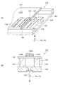
まず、有機EL装置1の製造に用いる液滴吐出装置について説明する。液滴吐出装置は、基板等のワークに対して相対移動可能なヘッドを有しており、このヘッドに設けられた吐出部から機能液等の液滴を吐出する装置である。図7(a)は、液滴吐出装置のヘッド114の斜視図であり、図7(b)は、当該ヘッド114の吐出部127の断面図である。
First, a droplet discharge device used for manufacturing the
図7(a)及び(b)に示すように、ヘッド114は、複数のノズル118を有するインクジェットヘッドである。具体的には、ヘッド114は、振動板126と、ノズル118の開口を規定するノズルプレート128とを備えている。そして、振動板126とノズルプレート128との間には、液たまり129が位置しており、この液たまり129には、図示しない外部タンクから孔131を介して供給される機能液14L(又は15L)が常に充填される。
As shown in FIGS. 7A and 7B, the
また、振動板126とノズルプレート128との間には、複数の隔壁部122が位置している。そして、振動板126と、ノズルプレート128と、一対の隔壁部122と、によって囲まれた部分がキャビティ120である。キャビティ120はノズル118に対応して設けられているため、キャビティ120の数とノズル118の数とは同じである。キャビティ120には、一対の隔壁部122間に位置する供給口130を介して、液たまり129から機能液14L(又は15L)が供給される。なお、本実施形態では、ノズル118の直径は、約27μmである。
A plurality of
振動板126上には、それぞれのキャビティ120に対応して、振動子124が配置されている。振動子124のそれぞれは、ピエゾ素子124Cと、ピエゾ素子124Cを挟む一対の電極124A,124Bとを含む。液滴吐出装置の制御部が、この一対の電極124A,124Bの間に駆動電圧を与えることで、対応するノズル118から機能液14Lの液滴が吐出される。ここで、ノズル118から吐出される材料の体積は、0pl以上42pl(ピコリットル)以下の間で可変である。
On the
1つのノズル118と、ノズル118に対応するキャビティ120と、キャビティ120に対応する振動子124と、を含んだ部分が吐出部127である。よって、1つのヘッド114は、ノズル118の数と同じ数の吐出部127を有する。吐出部127は、ピエゾ素子124Cの代わりに電気熱変換素子を有してもよい。つまり、吐出部127は、電気熱変換素子による材料の熱膨張を利用して材料を吐出する構成を有していてもよい。
A portion including one
続いて、図4に示す工程図に沿って有機EL装置1の製造方法について説明する。
Next, a method for manufacturing the
まず、ステップS1では、公知の成膜技術等を用いて、ガラス基板10の表面に回路素子層19を形成する。続くステップS2では、回路素子層19上に、ITOからなる画素電極11を形成する。
First, in step S1, the
次に、ステップS3では、回路素子層19及び画素電極11の上に、第1バンク12及び濡れ性可変バンク22pを形成する(図5(a))。より詳しくは、まず、第1バンク12の材料となる酸化シリコン(SiO2)を含んだ第1バンク材料の層を、常圧又は減圧CVD法等によりガラス基板10上の全体に、画素電極11を覆って形成する。次に、第1バンク材料の上に、濡れ性可変バンク22pの材料を含む塗工液を塗布して乾燥させ、濡れ性可変バンク材料の層を形成する。最後に、第1バンク材料及び濡れ性可変バンク材料のうち発光領域5に対応する領域に円形の開口部12aを形成して、第1バンク12及び濡れ性可変バンク22pが完成する。
Next, in step S3, the
ここで、濡れ性可変バンク22pの材料となる塗工液について説明する。当該塗工液は、ポリシロキサンと酸化チタンとを含んでいる。このうち酸化チタンは、光触媒として作用し、エネルギーを照射することによって表面の濡れ性を変化させるものである。酸化チタンの粒径は小さいほど光触媒反応が効果的に起こることから、平均粒径が50nm以下であることが好ましく、特に粒径が20nm以下の酸化チタンを使用することが好ましい。
Here, the coating liquid used as the material of the wettability
一方、上記ポリシロキサンは、撥液性を有する置換基が、ポリシロキサンを構成するSi原子に直接結合しているものである。ここで、撥液性を有する置換基としては、アルキル基、フルオロアルキル基、ビニル基、アミノ基、フェニル基、エポキシ基等が挙げられる。本実施形態ではフルオロアルキル基が用いられている。ポリシロキサンのこうした構造に起因して、上記塗工液から形成された濡れ性可変バンク22pは、撥液性を発現する。また、この濡れ性可変バンク22pにエネルギーが照射されると、上記光触媒の作用により上記置換基が分解等され、親液性を発現するようになる。すなわち、濡れ性可変バンク22pは、エネルギーが照射された領域のみ選択的に親液性が向上し、残りの領域は撥液性が保たれるという性質を持つ。
On the other hand, the polysiloxane has a liquid-repellent substituent directly bonded to Si atoms constituting the polysiloxane. Here, examples of the substituent having liquid repellency include an alkyl group, a fluoroalkyl group, a vinyl group, an amino group, a phenyl group, and an epoxy group. In this embodiment, a fluoroalkyl group is used. Due to such a structure of polysiloxane, the wettability
次に、ステップS4では、濡れ性可変バンク22pの表面の領域であって、発光領域5を囲む環状の領域A、領域Aを囲む環状の領域B、領域Bの外側の領域Cのうち、領域Bにエネルギーを照射する。これにより、領域Bの親液性を、領域A,Cより高めることができる。その結果、領域Aには第1撥液領域22aが形成され、領域Bには第1撥液領域22aより濡れ性の高い親液領域22bが形成され、領域Cには親液領域22bより濡れ性の低い第2撥液領域22cが形成される。こうして、第1撥液領域22a、親液領域22b、第2撥液領域22cを有する第2バンク22が形成される(図5(b))。このステップS4は、本発明におけるステップDに対応する。
Next, in step S4, the region of the surface of the wettability
ここで、上記エネルギー照射は、例えば、領域A及び領域Cを遮光して、領域Bに紫外線を照射して行う。本実施形態では、超高圧水銀ランプ(30mW/cm2、波長365nm)を30秒露光した。 Here, the energy irradiation is performed by, for example, shielding the region A and the region C and irradiating the region B with ultraviolet rays. In this embodiment, an ultrahigh pressure mercury lamp (30 mW / cm 2 , wavelength 365 nm) was exposed for 30 seconds.
こうして得られた第2バンク22が、後述するステップS5以降において機能液14L,15Lの濡れ広がる領域を規制する機能を有するためには、理論的には第1撥液領域22aと親液領域22b、及び親液領域22bと第2撥液領域22cの間に親液性の差が存在していれば良い。例えば、これら隣接する領域間で、機能液14L,15Lに対する接触角に1°以上の差があればよい。ただし、より好ましくは接触角に10°以上の差が現れるように上記領域Bにエネルギーを照射する。
In order for the
次に、ステップS5では、画素電極11上のうち、第1撥液領域22aに囲まれた領域(すなわち発光領域5)に、正孔注入層14の材料を含んだ機能液14Lを液滴吐出法により吐出する(図5(c))。より詳しくは、液滴吐出装置のヘッド114から、機能液14Lの液滴を、画素電極11を底部とし第1バンク12及び第2バンク22を側壁とする凹部の底部に向けて吐出する。ここで、上述したように、発光領域5の周囲には第1撥液領域22aが形成されているため、上記凹部に吐出された機能液14Lは、発光領域5の外には浸入しにくい。このステップS5で用いる機能液14Lとしては、例えばPEDOT−PSS分散液を用いることができる。PEDOT−PSS分散液の一例としては、PEDOTとPSSとの重量比が1:10、かつ固形分濃度が0.5%であり、ジエチレングリコールを50%含み、残量が純水であるものを用いることができる。
Next, in step S5, the
次に、ステップS6では、機能液14Lを乾燥させて正孔注入層14を形成する(図5(d))。より詳しくは、機能液14Lを高温環境下で乾燥又は焼成して溶媒を蒸発させ、機能液14Lに含まれるPEDOT−PSSを固形化させることにより、上記凹部に正孔注入層14を形成する。このステップS6における乾燥は、例えば200℃の環境下でガラス基板10を10分間放置する工程とすることができる。この乾燥工程中も、機能液14Lは、第1撥液領域22aの存在により発光装置5の外部へは侵入しにくい。このため、正孔注入層14を容易に発光領域5内に形成することができる。
Next, in step S6, the
次に、ステップS7では、正孔注入層14上及び第2バンク22上のうち、第2撥液領域22cに囲まれた領域(すなわち、発光領域5、第1撥液領域22a、親液領域22bからなる領域)に、発光層15の材料を含んだ機能液15Lを液滴吐出法により吐出する(図6(a))。より詳しくは、液滴吐出装置のヘッド114から、機能液15Lの液滴を、発光領域5、第1撥液領域22a、親液領域22bに向けて吐出する。このとき、ステップS4において形成された第2撥液領域22cの存在により、吐出された機能液15Lは、親液領域22b及びその内側の領域にのみ濡れ広がり、第2撥液領域22cには侵入しにくい。このステップS7で用いる機能液15Lとしては、例えば赤色蛍光材料を固形分濃度0.5%で含み、キシレンを溶媒とするものを用いることができる。また、このステップS7で用いる液滴吐出装置としては、正孔注入層14の形成の際に用いた液滴吐出装置において機能液14Lを機能液15Lに入れ替えたものであってもよいし、これとは異なる液滴吐出装置を用いてもよい。また、インクジェット法に代えてディスペンサ塗布法等を用いてもよい。
Next, in step S7, the region surrounded by the second liquid
次に、ステップS8では、機能液15Lを乾燥させて発光層15を形成する(図6(b))。より詳しくは、機能液15Lを高温環境下で乾燥又は焼成して溶媒を蒸発させ、機能液15Lに含まれる赤色蛍光材料を固形化させることにより、正孔注入層14上及び第2バンク22上のうち、第2撥液領域22cに囲まれた領域に発光層15を形成する。このステップS8における乾燥は、例えば100℃の環境下でガラス基板10を1時間放置する工程とすることができる。この乾燥工程中も、機能液15Lは、親液領域22b及びその内側の領域にのみ濡れ広がり、第2撥液領域22cへは侵入しにくい。このため、発光層15を容易に第2撥液領域22cに囲まれた領域に形成することができる。こうして形成された発光層15は、正孔注入層14(又は発光領域5)より大きな面積を有しているため、発光層15のうち比較的平坦な領域を発光に用いることができる。
Next, in step S8, the
次に、ステップS9では、発光層15の形成されたガラス基板10上の略全体に、カルシウム及びアルミニウムをこの順に積層させることにより、陰極16を形成する。本実施形態の製造方法によれば、第2バンク22における第1撥液領域22a、親液領域22b、第2撥液領域22cを利用することにより、凹凸の少ない平坦な面で発光層15のパターニングを行うことができる。これにより、発光層15が形成された状態における基板の表面(すなわち陰極16の形成領域)が平坦な状態となるため、陰極16を高品位に形成することができる。
Next, in step S9, the
続くステップS10では、陰極16上に、樹脂からなる封止部材17を形成する(図6(c))。なお、封止の方式は封止部材17によるものに限られず、シール剤を介してガラス基板等を貼り合わせる缶封止の方式等とすることもできる。
In subsequent step S10, a sealing
以上のステップを経て、有機EL装置1が完成する。こうして得られた有機EL装置1は、正孔注入層14の面積(すなわち発光領域5の面積)より大きな面積を有する発光層15が形成される。このため、発光領域5における発光層15の厚さが均一となる。これにより、発光層15のうち比較的平坦な部分を発光に用いることができ、簡便な製造プロセスで、均一な発光特性を有する有機EL装置1が得られる。特に、発光層15の形成に際して機能液15Lの吐出領域を規定するための有機バンクを形成する必要がないため、製造工程を簡略化することができる。
The
(電子機器)
本実施形態の有機EL装置1は、電子機器としての画像形成装置に搭載して用いることができる。より詳しくは、有機EL装置1は、画像形成装置に含まれる潜像書き込みヘッドモジュールに組み込んで用いることができる。
(Electronics)
The
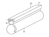
図8は、有機EL装置1をラインヘッドとして搭載した潜像書き込みヘッドモジュール101の斜視図である。潜像書き込みヘッドモジュール101は、円柱状の感光体ドラム41と平行に、これと対向した状態で用いられる。潜像書き込みヘッドモジュール101は、感光体ドラム41と平行な方向に配設された箱体37と、感光体ドラム41と箱体37との間に位置するように箱体37に取り付けられた光学部材38とを備えている。箱体37は、感光体ドラム41側に開口部を有しており、その開口部に向かって光が射出するように有機EL装置1が固定されている。
FIG. 8 is a perspective view of a latent image writing
また、図9の断面図に示すように、光学部材38は、有機EL装置1と対向する位置に備えられている。この光学部材38は、内部にセルフォック(登録商標)レンズアレイ39を備えており、有機EL装置1の発光領域5から射出され、一端に入射した光を、他端側から射出して感光体ドラム41の表面で集光、照射(露光)する。
Further, as shown in the cross-sectional view of FIG. 9, the
なお、上記発光層15の主発光波長(630nm)は、感光体ドラム41の感度の高い波長域から選択されたものである。このように、発光層15の発光波長は、感光体ドラム41の特性に応じて設定することが好ましく、感光体ドラム41の感度特性に応じて適宜選択することが可能である。
The main light emission wavelength (630 nm) of the
潜像書き込みヘッドモジュール101は、図10に示す画像形成装置80に用いられる。図10は、画像形成装置80の構造を示す断面図である。画像形成装置80は、有機EL装置1が組み込まれた潜像書き込みヘッドモジュール101K,101C,101M,101Yを備えている。ここで、上記符号中のK,C,M,Yは、それぞれ黒、シアン、マゼンタ、イエローを意味し、それぞれ黒、シアン、マゼンタ、イエロー用の潜像書き込みヘッドモジュールであることを示している。本明細書においては、上記潜像書き込みヘッドモジュール101K,101C,101M,101Yをまとめて指し示す場合には、符号(K,C,M,Y)を省略して単に「潜像書き込みヘッドモジュール101」と記載する。これらの符号(K,C,M,Y)の意味と、これを省略した場合の意味合いは、他の部材においても同様である。
The latent image writing
画像形成装置80には、潜像書き込みヘッドモジュール101K,101C,101M,101Yに対応して4個の感光体ドラム(像担持体)41K,41C,41M,41Yが配置されている。こうした構成は、タンデム方式と呼ばれる。感光体ドラム41は、その外周面が像担持体としての感光層となっている。
In the
この画像形成装置80は、駆動ローラ91と従動ローラ92とテンションローラ93とを備えている。これら各ローラには、中間転写ベルト90が、図10中矢印方向(反時計方向)に循環駆動するよう張架されている。4つの感光体ドラム41は、この中間転写ベルト90に沿って所定間隔で配置されている。感光体ドラム41は、中間転写ベルト90の駆動と同期して、図10中矢印方向(時計方向)に回転駆動するようになっている。
The
各感光体ドラム41の周囲には、感光体ドラム41の外周面を一様に帯電させる帯電装置(コロナ帯電器)42K,42C,42M,42Yと、この帯電装置42によって一様に帯電させられた外周面を感光体ドラム41の回転に同期して順次ライン走査する潜像書き込みヘッドモジュール101とが設けられている。潜像書き込みヘッドモジュール101は、有機EL装置1のアレイ方向(発光領域5の整列方向)が感光体ドラム41の回転軸に平行となるように設置されている。そして、潜像書き込みヘッドモジュール101の主発光波長と、感光体ドラム41の感度ピーク波長とが略一致するように設定されている。
Around each
また、潜像書き込みヘッドモジュール101で形成された静電潜像に現像剤であるトナーを付与して可視像(トナー像)とする現像装置44K,44C,44M,44Yと、これらの現像装置44で現像されたトナー像を一次転写対象である中間転写ベルト90に順次転写する転写手段としての一次転写ローラ45K,45C,45M,45Yとが設けられている。また、転写された後に感光体ドラム41の表面に残留しているトナーを除去するクリーニング手段としてのクリーニング装置46K,46C,46M,46Yが設けられている。
Further, developing
現像装置44は、例えば、現像剤として非磁性一成分トナーを用いる。そして、その一成分現像剤を例えば供給ローラで現像ローラへ搬送し、現像ローラ表面に付着した現像剤の膜厚を規制ブレードで規制し、その現像ローラを感光体ドラム41に接触させあるいは押圧せしめることにより、感光体ドラム41の電位レベルに応じて現像剤を付着させ、トナー像として現像するものである。
For example, the developing device 44 uses a non-magnetic one-component toner as a developer. Then, the one-component developer is conveyed to the developing roller by, for example, a supply roller, the film thickness of the developer adhering to the surface of the developing roller is regulated by a regulating blade, and the developing roller is brought into contact with or pressed against the
このような4色の単色トナー像形成ステーションにより形成された黒、シアン、マゼンタ、イエローの各トナー像は、一次転写ローラ45に印加される一次転写バイアスによって中間転写ベルト90上に順次一次転写される。そして、中間転写ベルト90上で順次重ね合わされてフルカラーとなったトナー像は、二次転写ローラ66において用紙等の記録媒体Pに二次転写され、さらに定着部である定着ローラ対61を通ることで記録媒体P上に定着される。その後、排紙ローラ対62によって装置上部に形成された排紙トレイ68上に排出される。
The black, cyan, magenta, and yellow toner images formed by the four-color single-color toner image forming station are sequentially primary transferred onto the
なお、図10中の符号63は多数枚の記録媒体Pが積層保持されている給紙カセット、64は給紙カセット63から記録媒体Pを一枚ずつ給送するピックアップローラ、65は二次転写ローラ66の二次転写部への記録媒体Pの供給タイミングを規定するゲートローラ対、67は二次転写後に中間転写ベルト90の表面に残留しているトナーを除去するクリーニング手段としてのクリーニングブレードである。
In FIG. 10,
このような構成の画像形成装置80において、潜像書き込みヘッドモジュール101は、有機EL装置1によって均一な発光を行うことができる。これにより、感光体ドラム41上に高精度に静電潜像を形成することができ、記録媒体Pにより高品位な画像を形成することができる。
In the
なお、本発明を適用した有機EL装置1は、上記画像形成装置80の他、プリンタヘッド、光ディスク用光源等の各種電子機器に搭載して用いることができる。
The
以上、本発明の実施形態について説明したが、上記実施形態に対しては、本発明の趣旨から逸脱しない範囲で様々な変形を加えることができる。変形例としては、例えば以下のようなものが考えられる。 As mentioned above, although embodiment of this invention was described, various deformation | transformation can be added with respect to the said embodiment in the range which does not deviate from the meaning of this invention. As modifications, for example, the following can be considered.
(変形例1)
上記実施形態の有機EL装置1は、単一の色の発光を行うものであるが、これに代えて、複数の色の発光を行うような構成とすることもできる。例えば、発光層15として、赤、緑、青の発光を行う発光層15R,15G,15Bを用いることにより、発光領域5ごとに異なる色の発光を行う有機EL装置1を構成することができる。この場合においても、発光層15R,15G,15Bは、いずれも第2撥液領域22cに囲まれた領域に形成される。そして、液滴吐出法によって発光層15R,15G,15Bを形成する際には、吐出された機能液15Lの濡れ広がる領域が第2撥液領域22cの存在によって規定されるため、凹凸のない面であっても容易に発光層15R,15G,15Bを塗り分けて形成することができる。以上のような構成を有する有機EL装置は、例えば携帯電話機等に表示装置として搭載して用いることができる。
(Modification 1)
The
(変形例2)
上記実施形態では、ステップS4において濡れ性可変バンク22pに照射するエネルギーとして、超高圧水銀ランプの紫外線を用いたが、これに限定する趣旨ではない。本発明でいうエネルギー照射とは、濡れ性可変バンク22pの濡れ性を変化させることが可能ないかなるエネルギー線の照射をも含む概念である。
(Modification 2)
In the above embodiment, the ultraviolet light of the ultra-high pressure mercury lamp is used as the energy applied to the wettability
本発明の実施に当たりエネルギー照射に用いられる光の波長は、400nm以下の範囲、好ましくは380nm以下の範囲から設定される。これは、濡れ性可変バンク22pに含まれる酸化チタンの光触媒作用を活性化させるエネルギーとして、上述した波長の光が好ましいからである。このようなエネルギー照射に用いることができる光源としては、水銀ランプ、メタルハライドランプ、キセノンランプ、エキシマランプ、その他種々の光源を挙げることができる。また、本発明においては、エキシマ、YAG等のレーザーを用いてエネルギー照射を行ってもよい。あるいは、第2バンク22上の領域Bを除いた領域にマスクを形成し、ガラス基板10をプラズマ処理して濡れ性可変バンク22pの表面状態を変化させる手法を用いることもできる。
In the practice of the present invention, the wavelength of light used for energy irradiation is set in the range of 400 nm or less, preferably in the range of 380 nm or less. This is because light having the above-described wavelength is preferable as energy for activating the photocatalytic action of titanium oxide contained in the wettability
(変形例3)
上記実施形態では、本発明における環状の領域(第1撥液領域22a及び親液領域22b)が円環状であり、かつ発光領域5が円形である場合について説明したが、これに限定する趣旨ではない。環状の領域は、四角環状、六角環状等の多角形からなる環状の領域であってもよいし、楕円環状等の曲線からなる環状の領域であっても良い。これらの場合においては、発光領域5の形状も当該環状の領域の形状に合わせて変形させることが好ましい。
(Modification 3)
In the above embodiment, the case where the annular regions (the first
1…「発光装置」としての有機EL装置、3…有機EL素子、5…発光領域、10…「基板」としてのガラス基板、11…画素電極、12…第1バンク、12a…開口部、14…正孔注入層、14L,15L…機能液、15…発光層、16…陰極、17…封止部材、19…回路素子層、22…第2バンク、22a…第1撥液領域、22b…親液領域、22c…第2撥液領域、22p…濡れ性可変バンク、27…TFT素子、80…「電子機器」としての画像形成装置、101…潜像書き込みヘッドモジュール。
DESCRIPTION OF
Claims (4)
基板と、
前記基板上に、前記発光領域ごとに形成された画素電極と、
前記基板上のうち、前記発光領域を除いた領域に形成され、かつ前記基板の法線方向から見て一部が前記画素電極の外縁部に重なった状態に形成された第1バンクと、
前記第1バンク上に形成され、前記発光領域を囲む環状の第1撥液領域、前記第1撥液領域を囲む環状の親液領域、及び前記親液領域の外側に配置された第2撥液領域を有する第2バンクと、
前記画素電極上のうち、前記第1撥液領域に囲まれた領域に配置された正孔注入層と、
前記正孔注入層上及び前記第2バンク上のうち、前記第2撥液領域に囲まれた領域に配置された発光層と、
前記発光層を挟んで前記画素電極の反対側に形成された陰極と、
を備え、
前記第2バンクにおける前記親液領域は、前記第1撥液領域及び前記第2撥液領域より濡れ性が高いことを特徴とする発光装置。 A light emitting device having a plurality of light emitting regions,
A substrate,
A pixel electrode formed on each of the light emitting regions on the substrate;
A first bank formed on a region of the substrate excluding the light emitting region and partially overlapped with an outer edge of the pixel electrode when viewed from a normal direction of the substrate;
An annular first lyophobic region formed on the first bank and surrounding the light emitting region, an annular lyophilic region surrounding the first lyophobic region, and a second repellant disposed outside the lyophilic region. A second bank having a liquid region;
A hole injection layer disposed in a region surrounded by the first liquid repellent region on the pixel electrode;
A light emitting layer disposed in a region surrounded by the second liquid repellent region on the hole injection layer and the second bank;
A cathode formed on the opposite side of the pixel electrode across the light emitting layer;
With
The light emitting device according to claim 1, wherein the lyophilic region in the second bank has higher wettability than the first liquid repellent region and the second liquid repellent region.
基板上に、前記発光領域ごとに画素電極を形成するステップと、
前記基板上に、前記画素電極を覆って、第1バンク材料、濡れ性可変バンク材料をこの順に積層させた後に、前記第1バンク材料及び前記濡れ性可変バンク材料のうち前記発光領域に対応する領域に開口部を形成することにより、第1バンク及び濡れ性可変バンクを形成するステップと、
前記濡れ性可変バンクの表面の領域であって、前記発光領域を囲む環状の領域A、前記領域Aを囲む環状の領域B、前記領域Bの外側の領域Cのうち、前記領域Bにエネルギーを照射することにより、前記領域Aに第1撥液領域を、前記領域Bに前記第1撥液領域より濡れ性の高い親液領域を、前記領域Cに前記親液領域より濡れ性の低い第2撥液領域をそれぞれ形成して、前記第1撥液領域、前記親液領域、前記第2撥液領域を有する第2バンクを形成するステップDと、
前記画素電極上のうち、前記第1撥液領域に囲まれた領域に、液滴吐出法により正孔注入層を形成するステップと、
前記正孔注入層上及び前記第2バンク上のうち、前記第2撥液領域に囲まれた領域に、液滴吐出法により発光層を形成するステップと、
前記発光層を挟んで前記画素電極の反対側に陰極を形成するステップと、
を備えることを特徴とする発光装置の製造方法。 A method of manufacturing a light emitting device having a plurality of light emitting regions,
Forming a pixel electrode for each light emitting region on a substrate;
A first bank material and a wettability variable bank material are stacked in this order on the substrate so as to cover the pixel electrode, and then correspond to the light emitting region of the first bank material and the wettability variable bank material. Forming the first bank and the wettability variable bank by forming an opening in the region;
The region B of the surface of the wettability variable bank, the annular region A surrounding the light emitting region, the annular region B surrounding the region A, and the region C outside the region B are energized in the region B. By irradiating, the region A has a first liquid repellent region, the region B has a higher lyophilic region than the first liquid repellent region, and the region C has a lower wettability than the lyophilic region. Forming two liquid repellent areas, respectively, and forming a second bank having the first liquid repellent area, the lyophilic area, and the second liquid repellent area; and
Forming a hole injection layer on the pixel electrode by a droplet discharge method in a region surrounded by the first liquid repellent region;
Forming a light emitting layer by a droplet discharge method in a region surrounded by the second liquid repellent region on the hole injection layer and the second bank;
Forming a cathode on the opposite side of the pixel electrode across the light emitting layer;
A method for manufacturing a light-emitting device.
前記ステップDは、前記領域A及び前記領域Cを遮光して前記領域Bに紫外線を照射するステップを含むことを特徴とする発光装置の製造方法。 A method for manufacturing a light emitting device according to claim 3,
The step D includes a step of shielding the region A and the region C and irradiating the region B with ultraviolet rays.
Priority Applications (1)
| Application Number | Priority Date | Filing Date | Title |
|---|---|---|---|
| JP2006267598A JP4788552B2 (en) | 2006-09-29 | 2006-09-29 | LIGHT EMITTING DEVICE, ELECTRONIC DEVICE, AND METHOD FOR MANUFACTURING LIGHT EMITTING DEVICE |
Applications Claiming Priority (1)
| Application Number | Priority Date | Filing Date | Title |
|---|---|---|---|
| JP2006267598A JP4788552B2 (en) | 2006-09-29 | 2006-09-29 | LIGHT EMITTING DEVICE, ELECTRONIC DEVICE, AND METHOD FOR MANUFACTURING LIGHT EMITTING DEVICE |
Publications (2)
| Publication Number | Publication Date |
|---|---|
| JP2008091051A JP2008091051A (en) | 2008-04-17 |
| JP4788552B2 true JP4788552B2 (en) | 2011-10-05 |
Family
ID=39375015
Family Applications (1)
| Application Number | Title | Priority Date | Filing Date |
|---|---|---|---|
| JP2006267598A Expired - Fee Related JP4788552B2 (en) | 2006-09-29 | 2006-09-29 | LIGHT EMITTING DEVICE, ELECTRONIC DEVICE, AND METHOD FOR MANUFACTURING LIGHT EMITTING DEVICE |
Country Status (1)
| Country | Link |
|---|---|
| JP (1) | JP4788552B2 (en) |
Families Citing this family (4)
| Publication number | Priority date | Publication date | Assignee | Title |
|---|---|---|---|---|
| JP4978543B2 (en) * | 2008-04-22 | 2012-07-18 | セイコーエプソン株式会社 | Organic electroluminescence device and manufacturing method thereof |
| JP6179310B2 (en) * | 2013-09-20 | 2017-08-16 | セイコーエプソン株式会社 | LIGHT EMITTING DEVICE AND ELECTRONIC DEVICE |
| JP6692900B2 (en) | 2016-05-18 | 2020-05-13 | 株式会社Joled | Organic EL display panel and manufacturing method thereof |
| JP6612446B2 (en) | 2016-06-09 | 2019-11-27 | 株式会社Joled | Organic EL display panel and manufacturing method thereof |
Family Cites Families (5)
| Publication number | Priority date | Publication date | Assignee | Title |
|---|---|---|---|---|
| JP2004235128A (en) * | 2002-12-04 | 2004-08-19 | Dainippon Printing Co Ltd | Organic EL element and method of manufacturing the same |
| JP3994998B2 (en) * | 2004-03-03 | 2007-10-24 | セイコーエプソン株式会社 | LIGHT EMITTING DEVICE, LIGHT EMITTING DEVICE MANUFACTURING METHOD, AND ELECTRONIC DEVICE |
| JP2006245526A (en) * | 2005-02-04 | 2006-09-14 | Seiko Epson Corp | Film pattern forming method, device and manufacturing method thereof, electro-optical device, and electronic apparatus |
| JP4715226B2 (en) * | 2005-02-21 | 2011-07-06 | セイコーエプソン株式会社 | ORGANIC ELECTROLUMINESCENT DEVICE, METHOD FOR PRODUCING ORGANIC ELECTROLUMINESCENT DEVICE, ELECTRONIC DEVICE |
| JP2006252838A (en) * | 2005-03-09 | 2006-09-21 | Seiko Epson Corp | ORGANIC EL DEVICE, METHOD FOR MANUFACTURING ORGANIC EL DEVICE, AND ELECTRONIC DEVICE |
-
2006
- 2006-09-29 JP JP2006267598A patent/JP4788552B2/en not_active Expired - Fee Related
Also Published As
| Publication number | Publication date |
|---|---|
| JP2008091051A (en) | 2008-04-17 |
Similar Documents
| Publication | Publication Date | Title |
|---|---|---|
| JP4766218B2 (en) | Organic EL array exposure head, manufacturing method thereof, and image forming apparatus using the same | |
| JP4539518B2 (en) | Electro-optical device and method of manufacturing electro-optical device | |
| KR100660591B1 (en) | Transparent substrate, electro-optical device, image forming device and method for manufacturing electro-optical device | |
| JP2009272276A (en) | Organic el device | |
| JP2006134624A (en) | Electro-optical device and electronic device using the same | |
| JP4508025B2 (en) | Line head, line head module, and image forming apparatus | |
| KR100695279B1 (en) | Method for manufacturing electro-optical device and image forming apparatus | |
| JP4788552B2 (en) | LIGHT EMITTING DEVICE, ELECTRONIC DEVICE, AND METHOD FOR MANUFACTURING LIGHT EMITTING DEVICE | |
| JP2010170767A (en) | Electro-optical device, light-emitting device, and electronic equipment | |
| KR100726274B1 (en) | Method for manufacturing transparent substrate, electro-optical device, image forming device, and electro-optical device | |
| JP4211710B2 (en) | Line head module and image forming apparatus | |
| JP2009176590A (en) | Organic EL device, method for manufacturing organic EL device, electronic device | |
| JP2010176937A (en) | Electro-optical device, light-emitting device, and electronic equipment | |
| JP5062206B2 (en) | Electro-optical device, electronic apparatus, and method of manufacturing electro-optical device | |
| JP5131234B2 (en) | Electro-optical device, electronic apparatus, and method of manufacturing electro-optical device | |
| JP2006119170A (en) | Transparent substrate, electro-optical device, image forming apparatus, and electro-optical device manufacturing method | |
| JP2008062541A (en) | Line head and image forming apparatus | |
| JP4281678B2 (en) | Electro-optical device manufacturing method and image forming apparatus | |
| JP2010280066A (en) | Organic electroluminescence device and image forming apparatus | |
| JP4238798B2 (en) | Line head, method for manufacturing line head, and image forming apparatus | |
| JP2008087202A (en) | Light emitting device and image forming apparatus | |
| JP2010182473A (en) | Electro-optical device, optical write-in head, image forming apparatus, and electronic apparatus | |
| JP4747793B2 (en) | Electro-optical device, method of manufacturing electro-optical device, and image forming apparatus | |
| JP5062205B2 (en) | Electro-optical device, electronic apparatus, and method of manufacturing electro-optical device | |
| JP2007220392A (en) | Electro-optical device manufacturing method and electro-optical device |
Legal Events
| Date | Code | Title | Description |
|---|---|---|---|
| A621 | Written request for application examination |
Free format text: JAPANESE INTERMEDIATE CODE: A621 Effective date: 20090722 |
|
| A977 | Report on retrieval |
Free format text: JAPANESE INTERMEDIATE CODE: A971007 Effective date: 20110113 |
|
| A131 | Notification of reasons for refusal |
Free format text: JAPANESE INTERMEDIATE CODE: A131 Effective date: 20110125 |
|
| TRDD | Decision of grant or rejection written | ||
| A01 | Written decision to grant a patent or to grant a registration (utility model) |
Free format text: JAPANESE INTERMEDIATE CODE: A01 Effective date: 20110621 |
|
| A01 | Written decision to grant a patent or to grant a registration (utility model) |
Free format text: JAPANESE INTERMEDIATE CODE: A01 |
|
| A61 | First payment of annual fees (during grant procedure) |
Free format text: JAPANESE INTERMEDIATE CODE: A61 Effective date: 20110704 |
|
| FPAY | Renewal fee payment (event date is renewal date of database) |
Free format text: PAYMENT UNTIL: 20140729 Year of fee payment: 3 |
|
| R150 | Certificate of patent or registration of utility model |
Free format text: JAPANESE INTERMEDIATE CODE: R150 |
|
| LAPS | Cancellation because of no payment of annual fees |