JP4780943B2 - Laser irradiation apparatus and method for manufacturing semiconductor device - Google Patents
Laser irradiation apparatus and method for manufacturing semiconductor device Download PDFInfo
- Publication number
- JP4780943B2 JP4780943B2 JP2004261235A JP2004261235A JP4780943B2 JP 4780943 B2 JP4780943 B2 JP 4780943B2 JP 2004261235 A JP2004261235 A JP 2004261235A JP 2004261235 A JP2004261235 A JP 2004261235A JP 4780943 B2 JP4780943 B2 JP 4780943B2
- Authority
- JP
- Japan
- Prior art keywords
- laser
- optical system
- pulse
- laser light
- energy distribution
- Prior art date
- Legal status (The legal status is an assumption and is not a legal conclusion. Google has not performed a legal analysis and makes no representation as to the accuracy of the status listed.)
- Expired - Fee Related
Links
Images


Description
本発明は、半導体膜の結晶化に用いることができるレーザ照射装置に関する。また該レーザ照射装置を用いたレーザ照射方法及び半導体装置の作製方法に関する。 The present invention relates to a laser irradiation apparatus that can be used for crystallization of a semiconductor film. Further, the present invention relates to a laser irradiation method using the laser irradiation apparatus and a method for manufacturing a semiconductor device.
多結晶半導体膜を用いた薄膜トランジスタ(多結晶TFT)は、非晶質半導体膜を用いたTFTに比べて移動度が2桁以上高く、半導体表示装置の画素部とその周辺の駆動回路を同一基板上に一体形成できるという利点を有している。 A thin film transistor using a polycrystalline semiconductor film (polycrystalline TFT) has a mobility that is two orders of magnitude higher than that of a TFT using an amorphous semiconductor film, and a pixel portion of a semiconductor display device and its peripheral drive circuit are formed on the same substrate. It has the advantage that it can be integrally formed on top.
多結晶半導体膜は、レーザアニール法を用いることで、安価なガラス基板上に形成することができる。レーザはその発振方法により、パルス発振と連続発振の2種類に大別することができる。エキシマレーザに代表されるパルス発振のレーザは、連続発振のレーザと比べて、単位時間あたりのレーザ光の出力エネルギーが3〜6桁程度高い。よって、ビームスポット(被処理物の表面において実際にレーザ光が照射される照射領域)を数cm角の矩形状または楕円状や、長さ100mm以上の線状となるように光学系にて成形することで、半導体膜へのレーザ光の照射を効率的に行ない、スループットを高めることができるというメリットを有している。 The polycrystalline semiconductor film can be formed over an inexpensive glass substrate by using a laser annealing method. Lasers can be broadly classified into two types, pulse oscillation and continuous oscillation, depending on the oscillation method. A pulsed laser typified by an excimer laser has an output energy of laser light per unit time of about 3 to 6 digits higher than that of a continuous wave laser. Therefore, the beam spot (irradiation area where the laser beam is actually irradiated on the surface of the object to be processed) is shaped by an optical system so as to have a rectangular or elliptical shape of several centimeters or a linear shape with a length of 100 mm or more. By doing so, there is an advantage that the semiconductor film can be efficiently irradiated with laser light and the throughput can be increased.
特に、半導体表示装置の画素部全体が収まるように成形された面状のビームスポットを用いることで、レーザ光の各パルス間で数%のエネルギーの揺らぎが生じても、該エネルギーの揺らぎにより半導体膜の結晶性がばらつくという事態を回避することができる。また、ビームスポットのエッジ部分によって形成される半導体膜の結晶性の劣っている部分が、画素部に形成されるのを防ぐことができる。従って、画素部全体が収まるような比較的広い範囲をカバーすることができるビームスポットを用いることで、結晶化を均一に行なうことができ、結晶化された多結晶半導体膜を活性層として用いるTFTの特性、例えばオン電流、移動度等のばらつきを抑えることができる。 In particular, by using a planar beam spot shaped so that the entire pixel portion of a semiconductor display device can be accommodated, even if a fluctuation of several percent of energy occurs between each pulse of a laser beam, the fluctuation of the energy causes a semiconductor. A situation in which the crystallinity of the film varies can be avoided. In addition, it is possible to prevent a portion where the crystallinity of the semiconductor film formed by the edge portion of the beam spot is inferior from being formed in the pixel portion. Therefore, by using a beam spot that can cover a relatively wide range in which the entire pixel portion can be accommodated, crystallization can be performed uniformly, and a TFT using a crystallized polycrystalline semiconductor film as an active layer Variations in characteristics such as on-current and mobility can be suppressed.
このように比較的広い範囲をカバーすることができる面状のビームスポットを用いることで、レーザ結晶化を均一に行なうことできると考えられるが、これはビームスポットの面内におけるエネルギーの分布が均一であることが前提である。例えばエキシマレーザの場合、ビームスポットの面内において、レーザ発振器に起因すると考えられるエネルギー分布が、P−V(Peak to Valley)値1%〜5%程度、実際に生じており、上記エネルギー分布によって、半導体膜の結晶性にばらつきが生じてしまう。そしてこの面内におけるエネルギーの分布は、パルス間でほぼ同じため、結晶性をより高めることを目的として同じ領域に複数パルス照射して結晶化を行なう場合、面内のエネルギー分布に起因する結晶性のばらつきが増幅され、かえって結晶性の均一化が妨げられてしまう。 It is thought that laser crystallization can be performed uniformly by using a planar beam spot that can cover a relatively wide range as described above, but this is because the energy distribution in the plane of the beam spot is uniform. It is a premise. For example, in the case of an excimer laser, an energy distribution that is considered to be caused by a laser oscillator is actually generated in a plane of a beam spot with a PV (Peak to Valley) value of about 1% to 5%. As a result, the crystallinity of the semiconductor film varies. And since the energy distribution in this plane is almost the same between pulses, when crystallization is performed by irradiating multiple pulses to the same region for the purpose of further improving the crystallinity, the crystallinity caused by the energy distribution in the plane As a result, the dispersion of the crystallinity is amplified and the uniformity of crystallinity is hindered.
なお、複数のレンズを備えたレンズアレイ等を用いたビームホモジナイザをレーザ光の光路に設けることで、面内におけるエネルギーの分布をある程度均一化させることができる。しかし、上記ビームホモジナイザによるエネルギーの均一化にも限界があり、エネルギー分布を完全に均一化することは難しい。単位面積あたりのレンズの数を増やすことで、幾何学的にレーザービームのエネルギー分布を均一化させることは可能である。しかし、単位体積あたりのレンズの数を増やすことで、各レンズ同士の光の干渉に起因するレーザ光のエネルギー密度のばらつきが増幅され、周期性を有する干渉縞として出現する可能性も有る。さらに、レンズが小型化されるため、より高い精度を有するレンズが必要となり、光学系が高価となり好ましくない。 By providing a beam homogenizer using a lens array having a plurality of lenses in the optical path of the laser light, the energy distribution in the surface can be made uniform to some extent. However, there is a limit to the homogenization of energy by the beam homogenizer, and it is difficult to make the energy distribution completely uniform. By increasing the number of lenses per unit area, it is possible to geometrically uniformize the energy distribution of the laser beam. However, by increasing the number of lenses per unit volume, variations in the energy density of the laser light due to the light interference between the lenses are amplified, and there is a possibility of appearing as interference fringes having periodicity. Furthermore, since the lens is miniaturized, a lens having higher accuracy is required, and the optical system is expensive, which is not preferable.
本発明は上述した問題に鑑み、ビームスポットの面内におけるエネルギー分布を抑えることができる、レーザ照射装置、レーザ照射方法及び前記レーザ照射方法を用いる半導体装置の作製方法の提供を課題とする。 In view of the above-described problems, an object of the present invention is to provide a laser irradiation apparatus, a laser irradiation method, and a method for manufacturing a semiconductor device using the laser irradiation method, which can suppress the energy distribution in the plane of the beam spot.
本発明者らは、1パルスのビームスポットの、面内におけるエネルギー分布が存在していても、同一領域に照射される複数パルスのビームスポット間でエネルギー分布を変えることで、結晶性のばらつきを抑えることができるのではないかと考えた。面内におけるエネルギー分布を変えるために、本発明では、(イ)同一領域に照射される複数パルスのうち、少なくとも1つのパルスの空間的なエネルギー分布を変えるための光学系を用いるか、または(ロ)同一領域に照射される複数パルスのうち、少なくとも1つのパルスにおいて、ビームホモジナイザのレンズアレイに入射するレーザ光の位置を変えるか、いずれかの方法を用いる。なお、本明細書中でのエネルギー分布とは、照射面内に形成されるビームスポット内のエネルギー分布を示す。 The present inventors can vary the crystallinity by changing the energy distribution among the beam spots of a plurality of pulses irradiated to the same region even if there is an in-plane energy distribution of the beam spot of one pulse. I thought it could be suppressed. In order to change the energy distribution in the plane, the present invention uses (a) an optical system for changing the spatial energy distribution of at least one pulse among a plurality of pulses irradiated to the same region, or ( (B) In at least one pulse among a plurality of pulses irradiated to the same region, the position of the laser beam incident on the lens array of the beam homogenizer is changed, or any method is used. In addition, the energy distribution in this specification shows the energy distribution in the beam spot formed in an irradiation surface.
具体的に(イ)のレーザ照射方法では、同一領域に照射される全パルスのレーザ光のうち、少なくとも1パルスの空間的なエネルギー分布を、光学系を用いて反転または回転させる。反転は、対称の中心となる直線が互いに交差するパルスどうしを組み合わせても良い。また、反転したパルスと回転したパルスとを組み合わせても良い。 Specifically, in the laser irradiation method (a), the spatial energy distribution of at least one pulse among all the laser beams irradiated to the same region is reversed or rotated using an optical system. The inversion may be a combination of pulses in which straight lines that are the centers of symmetry intersect each other. Further, an inverted pulse and a rotated pulse may be combined.
また(イ)のレーザ照射方法を用いるレーザ照射装置は、パルス発振でレーザ光を出力するレーザ発振器と、複数の光学系を有するレンズアッセンブリと、前記レーザ光が有する複数のパルスに同期して前記レンズアッセンブリの位置を制御することで、前記複数の光学系から少なくとも2つを選択する位置制御手段とを有する。前記複数の光学系によって、前記複数のパルスから、空間的なエネルギー分布が互いに反転または回転した複数のパルスを形成することができる。さらに、前記エネルギー分布が互いに反転または回転した複数の各パルスの、前記エネルギー分布を均一化し、同一領域に照射するためのビームホモジナイザとを有していても良い。 In addition, a laser irradiation apparatus using the laser irradiation method (A) includes a laser oscillator that outputs laser light by pulse oscillation, a lens assembly having a plurality of optical systems, and a plurality of pulses that the laser light has. Position control means for selecting at least two of the plurality of optical systems by controlling the position of the lens assembly. The plurality of optical systems can form a plurality of pulses whose spatial energy distributions are reversed or rotated from each other from the plurality of pulses. Further, a beam homogenizer may be provided for uniformizing the energy distribution of each of the plurality of pulses whose energy distributions are inverted or rotated with respect to each other and irradiating the same region.
具体的に(ロ)のレーザ照射方法では、レーザ光の面内のエネルギー分布が存在している場合、レンズアレイに入射する位置を変えることで、該レンズアレイに含まれる各レンズに入射するレーザ光のエネルギー分布が変化する。したがって、レンズアレイの入射位置を変える前と、変えた後とでは、ビームスポットの面内におけるエネルギー分布に変化が生じることになる。 Specifically, in the laser irradiation method of (b), when there is an in-plane energy distribution of the laser light, the laser incident on each lens included in the lens array is changed by changing the position incident on the lens array. The light energy distribution changes. Therefore, the energy distribution in the plane of the beam spot changes before and after the incident position of the lens array is changed.
また(ロ)のレーザ照射方法を用いるレーザ照射装置は、パルス発振でレーザ光を出力するレーザ発振器と、レンズアレイを有するビームホモジナイザと、前記レーザ光が有する複数のパルスに同期して前記レンズアレイの位置を制御することで、前記レーザ光が前記レンズアレイに入射する位置を制御する位置制御手段とを有する。さらに、前記レンズアレイから射出したレーザ光を同一の領域に照射するための集光レンズ等の光学系とを有していても良い。 A laser irradiation apparatus using the laser irradiation method (b) includes a laser oscillator that outputs laser light by pulse oscillation, a beam homogenizer having a lens array, and the lens array in synchronization with a plurality of pulses of the laser light. Position control means for controlling the position at which the laser beam is incident on the lens array. Furthermore, an optical system such as a condensing lens for irradiating the same region with laser light emitted from the lens array may be provided.
本発明では、上記(イ)または(ロ)の構成を用いることにより、同一領域に照射されるレーザ光の、トータルのエネルギー分布が平均化される。そしてさらに、上記(イ)または(ロ)の構成を互いに組み合わせることで、トータルのエネルギー分布をより平均化することができる。 In the present invention, the total energy distribution of the laser light irradiated to the same region is averaged by using the configuration (a) or (b). Furthermore, the total energy distribution can be further averaged by combining the configurations (a) and (b).
なお、エネルギー分布は、1パルスごとに変化させることがトータルのエネルギー分布を平均化させるのに最も効果的である。しかし本発明はこの構成に限定されず、同一領域に照射される複数パルスのうち、少なくとも1つのパルスの空間的なエネルギー分布を変えればよい。 Note that changing the energy distribution for each pulse is most effective for averaging the total energy distribution. However, the present invention is not limited to this configuration, and it is only necessary to change the spatial energy distribution of at least one pulse among a plurality of pulses irradiated to the same region.
なお本発明の半導体装置の作製方法は、具体的には集積回路や半導体表示装置の作製方法に用いることができる。特に、液晶表示装置、有機発光素子に代表される発光素子を各画素に備えた発光装置、DMD(Digital Micromirror Device)、PDP(Plasma Display Panel)、FED(Field Emission Display)等の半導体表示装置の画素部に設けられたトランジスタ等の半導体素子に用いた場合、画素部において照射されたレーザ光のエネルギーの分布に起因する輝度むらが、視認されるのを抑えることができる。特にTFTの場合、結晶化を均一に行なうことで、TFTの特性、例えばオン電流、移動度等のばらつきを抑えることができる。 Note that the method for manufacturing a semiconductor device of the present invention can be specifically used for a method for manufacturing an integrated circuit or a semiconductor display device. In particular, a liquid crystal display device, a light emitting device including a light emitting element typified by an organic light emitting element in each pixel, a semiconductor display device such as a DMD (Digital Micromirror Device), a PDP (Plasma Display Panel), and an FED (Field Emission Display). When used for a semiconductor element such as a transistor provided in the pixel portion, it is possible to suppress the luminance unevenness caused by the energy distribution of the laser light irradiated in the pixel portion from being visually recognized. In particular, in the case of TFTs, variation in TFT characteristics such as on-current and mobility can be suppressed by performing crystallization uniformly.
なお本発明はエキシマレーザのみならず、ガラスレーザ、YAGレーザ、YVO4レーザ、GdVO4レーザや、その他のパルス発振型のレーザにも適用することができる。また発振方法もパルス発振だけに限定されず、連続発振のレーザ装置に適用しても良い。 Note that the present invention can be applied not only to excimer lasers but also to glass lasers, YAG lasers, YVO 4 lasers, GdVO 4 lasers, and other pulsed lasers. The oscillation method is not limited to pulse oscillation, and may be applied to a continuous oscillation laser device.
本発明のレーザ照射装置は、パルス発振でレーザ光を出力するレーザ発振器と、複数の光学系を有するレンズアッセンブリと、パルス発振と同期してレンズアッセンブリの位置を制御する位置制御手段とを有することを特徴とする。 The laser irradiation apparatus of the present invention includes a laser oscillator that outputs laser light by pulse oscillation, a lens assembly having a plurality of optical systems, and a position control unit that controls the position of the lens assembly in synchronization with pulse oscillation. It is characterized by.
本発明のレーザ照射装置は、パルス発振でレーザ光を出力するレーザ発振器と、複数の光学系を有するレンズアッセンブリと、レンズアッセンブリの位置を制御することによって、複数の光学系から少なくとも2つの光学系を選択する位置制御手段とを有することを特徴とする。 The laser irradiation apparatus of the present invention includes a laser oscillator that outputs laser light by pulse oscillation, a lens assembly having a plurality of optical systems, and at least two optical systems from the plurality of optical systems by controlling the positions of the lens assemblies. And position control means for selecting.
本発明のレーザ照射装置は、パルス発振でレーザ光を出力するレーザ発振器と、複数の光学系を有するレンズアッセンブリと、パルス発振に同期してレンズアッセンブリの位置を制御することで、複数の光学系から少なくとも2つの光学系を選択する位置制御手段とを有し、選択された少なくとも2つの光学系は、第1の光学系および第2の光学系を含み、第1の光学系における空間的なエネルギー分布の反転または回転の軸と、第2の光学系における空間的なエネルギー分布の反転または回転の軸が、互いに交差することを特徴とする。 The laser irradiation apparatus of the present invention includes a laser oscillator that outputs laser light by pulse oscillation, a lens assembly having a plurality of optical systems, and a plurality of optical systems by controlling the position of the lens assembly in synchronization with the pulse oscillation. Position control means for selecting at least two optical systems from the above, and the at least two selected optical systems include a first optical system and a second optical system, and the spatial in the first optical system An axis of inversion or rotation of the energy distribution and an axis of inversion or rotation of the spatial energy distribution in the second optical system intersect with each other.
本発明のレーザ照射装置は、パルス発振でレーザ光を出力するレーザ発振器と、レンズアレイ及び光学系を有するビームホモジナイザと、レンズアレイの位置を制御する位置制御手段とを有することを特徴とする。 The laser irradiation apparatus of the present invention includes a laser oscillator that outputs laser light by pulse oscillation, a beam homogenizer having a lens array and an optical system, and a position control unit that controls the position of the lens array.
本発明のレーザ照射装置は、パルス発振でレーザ光を出力するレーザ発振器と、複数の光学系を有するレンズアッセンブリと、パルス発振に同期してレンズアッセンブリの位置を制御する第1の位置制御手段と、レンズアレイ及び光学系を有するビームホモジナイザと、レンズアレイの位置を制御する第2の位置制御手段を有することを特徴とする。 A laser irradiation apparatus of the present invention includes a laser oscillator that outputs laser light by pulse oscillation, a lens assembly having a plurality of optical systems, and first position control means that controls the position of the lens assembly in synchronization with pulse oscillation. And a beam homogenizer having a lens array and an optical system, and second position control means for controlling the position of the lens array.
本発明のレーザ照射方法は、空間的なエネルギー分布の異なる複数のパルスを有するレーザ光を、同一領域に照射することを特徴とする。 The laser irradiation method of the present invention is characterized in that the same region is irradiated with laser light having a plurality of pulses having different spatial energy distributions.
本発明のレーザ照射方法は、パルス発振でレーザ光を出力するレーザ発振器と、複数の光学系を有するレンズアッセンブリと、パルス発振に同期してレンズアッセンブリの位置を制御する位置制御手段とを有するレーザ照射装置において、パルス発振に同期して、前記レンズアッセンブリの位置を制御することにより、レンズアッセンブリが有する複数の光学系のうち少なくとも2つの光学系が選択され、選択された少なくとも2つの光学系によって、レーザ光の空間的なエネルギー分布が互いに反転または回転することを特徴とする。 The laser irradiation method of the present invention is a laser having a laser oscillator for outputting laser light by pulse oscillation, a lens assembly having a plurality of optical systems, and a position control means for controlling the position of the lens assembly in synchronization with pulse oscillation. In the irradiation apparatus, by controlling the position of the lens assembly in synchronization with the pulse oscillation, at least two optical systems among the plurality of optical systems included in the lens assembly are selected, and the selected at least two optical systems The spatial energy distribution of the laser light is inverted or rotated with respect to each other.
本発明のレーザ照射方法は、パルス発振でレーザ光を出力するレーザ発振器と、レンズアレイ及び光学系を有するビームホモジナイザと、レーザ光がレンズアレイの位置を制御する位置制御手段とを有するレーザ照射装置において、パルス発振に同期してレンズアレイの位置を制御することで、レーザ光がレンズアレイに入射する位置を制御し、レンズアレイから射出したレーザ光を光学系により同一領域に照射することを特徴とする。 The laser irradiation method of the present invention includes a laser oscillator that outputs laser light by pulse oscillation, a beam homogenizer having a lens array and an optical system, and a position control means for controlling the position of the lens array by the laser light. The position of the lens array is controlled in synchronization with the pulse oscillation to control the position where the laser light is incident on the lens array, and the laser light emitted from the lens array is irradiated to the same region by the optical system. And
本発明のレーザ照射方法は、パルス発振でレーザ光を出力するレーザ発振器と、レンズアレイ及び光学系を有するビームホモジナイザと、レーザ光がレンズアレイの位置を制御する位置制御手段とを有するレーザ照射装置において、パルス発振に同期してレンズアレイの位置を制御することで、レーザ光が前記レンズアレイに入射する位置を制御し、レンズアレイから射出したレーザ光を光学系により半導体膜の同一領域に照射することを特徴とする。 The laser irradiation method of the present invention includes a laser oscillator that outputs laser light by pulse oscillation, a beam homogenizer having a lens array and an optical system, and a position control means for controlling the position of the lens array by the laser light. The position of the lens array is controlled in synchronization with the pulse oscillation to control the position where the laser light enters the lens array, and the laser light emitted from the lens array is irradiated to the same region of the semiconductor film by the optical system. It is characterized by doing.
本発明のレーザ照射方法は、パルス発振でレーザ光を出力するレーザ発振器と、複数の光学系を有するレンズアッセンブリと、パルス発振に同期してレンズアッセンブリの位置を制御する位置制御手段とを有するレーザ照射装置において、パルス発振に同期して、レンズアッセンブリの位置を制御することにより、レンズアッセンブリが有する複数の光学系のうち少なくとも2つの光学系が選択され、選択された少なくとも2つの光学系によって、レーザ光の空間的なエネルギー分布が互いに反転または回転した複数のパルスが形成され、空間的なエネルギー分布が互いに反転または回転した複数のパルスを、同一領域に照射することを特徴とする。 The laser irradiation method of the present invention is a laser having a laser oscillator for outputting laser light by pulse oscillation, a lens assembly having a plurality of optical systems, and a position control means for controlling the position of the lens assembly in synchronization with pulse oscillation. In the irradiation apparatus, by controlling the position of the lens assembly in synchronization with the pulse oscillation, at least two optical systems of the plurality of optical systems included in the lens assembly are selected, and by the selected at least two optical systems, A plurality of pulses in which the spatial energy distribution of the laser light is reversed or rotated are formed, and the same region is irradiated with a plurality of pulses whose spatial energy distributions are reversed or rotated.
本発明のレーザ照射方法は、パルス発振でレーザ光を出力するレーザ発振器と、複数の光学系を有するレンズアッセンブリと、パルス発振に同期してレンズアッセンブリの位置を制御する位置制御手段とを有するレーザ照射装置において、パルス発振に同期して、前記レンズアッセンブリの位置を制御することにより、レンズアッセンブリが有する複数の光学系のうち少なくとも第1の光学系および第2の光学系が選択され、第1の光学系により第1の直線を軸中心としてレーザ光の空間的なエネルギー分布が互いに反転したパルスが形成され、第2の光学系により第2の直線を軸中心としてレーザ光の空間的なエネルギー分布が互いに反転したパルスが形成され、第1の直線と第2の直線とは、互いに交差することを特徴とする。 The laser irradiation method of the present invention is a laser having a laser oscillator for outputting laser light by pulse oscillation, a lens assembly having a plurality of optical systems, and a position control means for controlling the position of the lens assembly in synchronization with pulse oscillation. In the irradiation apparatus, by controlling the position of the lens assembly in synchronization with pulse oscillation, at least the first optical system and the second optical system are selected from among the plurality of optical systems included in the lens assembly. In this optical system, pulses in which the spatial energy distributions of the laser light are inverted with respect to each other about the first straight line are formed, and the spatial energy of the laser light about the second straight line as the axial center is formed by the second optical system. Pulses whose distributions are reversed from each other are formed, and the first straight line and the second straight line intersect each other.
本発明のレーザ照射方法は、パルス発振でレーザ光を出力するレーザ発振器と、複数の光学系を有するレンズアッセンブリと、パルス発振に同期してレンズアッセンブリの位置を制御する第1の位置制御手段と、レンズアレイ及び第1の光学系を有するビームホモジナイザと、レンズアレイの位置を制御する第2の位置制御手段を有するレーザ照射装置において、パルス発振に同期して、レンズアッセンブリの位置を制御することによって、レンズアッセンブリが有する複数の光学系のうち少なくとも第2の光学系及び第3の光学系が選択され、第2の光学系により第1の直線を軸中心としてレーザ光の空間的なエネルギー分布が互いに反転した第1のパルスが形成され、第3の光学系により第2の直線を軸中心としてレーザ光の空間的なエネルギー分布が互いに反転した第2のパルスが形成され、レンズアッセンブリの位置を制御することにより、少なくとも第1のパルスおよび前記第2のパルスを含む複数のパルスが形成され、空間的なエネルギー分布が互いに反転または回転した複数のパルスは、ビームホモジナイザによって前記空間的なエネルギー分布が均一化され、第1の光学系により同一領域に照射され、第1の直線と第2の直線とは、互いに交差することを特徴とする。 The laser irradiation method of the present invention includes a laser oscillator that outputs laser light by pulse oscillation, a lens assembly having a plurality of optical systems, and first position control means that controls the position of the lens assembly in synchronization with pulse oscillation. In a laser irradiation apparatus having a beam homogenizer having a lens array and a first optical system and a second position control means for controlling the position of the lens array, the position of the lens assembly is controlled in synchronization with pulse oscillation. Thus, at least the second optical system and the third optical system are selected from among the plurality of optical systems of the lens assembly, and the spatial energy distribution of the laser light with the first straight line as the axis center is selected by the second optical system. The first pulses in which the laser beams are inverted from each other are formed, and the spatial light of the laser beam is centered on the second straight line by the third optical system. A second pulse having inverted ruby distribution is formed, and by controlling the position of the lens assembly, a plurality of pulses including at least the first pulse and the second pulse are formed, and the spatial energy distribution is A plurality of pulses that are inverted or rotated from each other are made uniform in the spatial energy distribution by a beam homogenizer, irradiated to the same region by the first optical system, and the first straight line and the second straight line intersect each other. It is characterized by doing.
本発明のレーザ照射方法は、パルス発振でレーザ光を出力するレーザ発振器と、複数の光学系を有するレンズアッセンブリと、パルス発振に同期してレンズアッセンブリの位置を制御する第1の位置制御手段と、レンズアレイ及び第1の光学系を有するビームホモジナイザと、レンズアレイの位置を制御する第2の位置制御手段を有するレーザ照射装置において、パルス発振に同期して、レンズアッセンブリの位置を制御することにより、前記レンズアッセンブリが有する複数の光学系のうち少なくとも2つの光学系が選択され、選択された少なくとも2つの光学系によって、レーザ光の空間的なエネルギー分布が互いに反転または回転した複数のパルスが形成され、エネルギー分布が互いに反転または回転した複数のパルスは、ビームホモジナイザによって空間的なエネルギー分布が均一化され、第1の光学系により半導体膜の同一領域に照射されることを特徴とする。 The laser irradiation method of the present invention includes a laser oscillator that outputs laser light by pulse oscillation, a lens assembly having a plurality of optical systems, and first position control means that controls the position of the lens assembly in synchronization with pulse oscillation. In a laser irradiation apparatus having a beam homogenizer having a lens array and a first optical system and a second position control means for controlling the position of the lens array, the position of the lens assembly is controlled in synchronization with pulse oscillation. Accordingly, at least two optical systems are selected from among the plurality of optical systems included in the lens assembly, and a plurality of pulses in which the spatial energy distribution of the laser light is inverted or rotated by the selected at least two optical systems. Multiple pulses that are formed and whose energy distributions are reversed or rotated from each other Spatial energy distribution by Naiza is made uniform, characterized in that it is irradiated in the same region of the semiconductor film by the first optical system.
本発明のレーザ照射方法は、パルス発振でレーザ光を出力するレーザ発振器と、複数の光学系を有するレンズアッセンブリと、パルス発振に同期してレンズアッセンブリの位置を制御する第1の位置制御手段と、レンズアレイ及び第1の光学系を有するビームホモジナイザと、レンズアレイの位置を制御する第2の位置制御手段を有するレーザ照射装置において、パルス発振に同期してレンズアッセンブリの位置を制御することによって、レンズアッセンブリが有する複数の光学系のうち少なくとも第2の光学系及び第3の光学系が選択され、第2の光学系により第1の直線を軸中心としてレーザ光の空間的なエネルギー分布が互いに反転した第1のパルスが形成され、第3の光学系により第2の直線を軸中心としてレーザ光の空間的なエネルギー分布が互いに反転した第2のパルスが形成され、レンズアッセンブリの位置を制御することにより、少なくとも第1のパルスおよび第2のパルスを含む複数のパルスが形成され、選択された少なくとも2つの光学系により形成された複数のパルスは、ビームホモジナイザによって前記空間的なエネルギー分布が均一化され、第1の光学系により半導体膜の同一領域に照射され、第1の直線と第2の直線とは、互いに交差することを特徴とする。 The laser irradiation method of the present invention includes a laser oscillator that outputs laser light by pulse oscillation, a lens assembly having a plurality of optical systems, and first position control means that controls the position of the lens assembly in synchronization with pulse oscillation. In a laser irradiation apparatus having a beam homogenizer having a lens array and a first optical system, and a second position control means for controlling the position of the lens array, by controlling the position of the lens assembly in synchronization with pulse oscillation , At least a second optical system and a third optical system are selected from among a plurality of optical systems included in the lens assembly, and a spatial energy distribution of the laser light is centered on the first straight line by the second optical system. A first pulse that is inverted with respect to each other is formed, and the spatial energy of the laser light is centered on the second straight line by the third optical system. A second pulse having a reversed Gee distribution is formed, and by controlling the position of the lens assembly, a plurality of pulses including at least the first pulse and the second pulse are formed, and the selected at least two optical The plurality of pulses formed by the system are uniformized in the spatial energy distribution by a beam homogenizer, irradiated to the same region of the semiconductor film by the first optical system, and the first straight line and the second straight line are , Crossing each other.
本発明は上記構成により、1パルスだけでみると面内のエネルギー分布が存在していたとしても、同一領域に照射されるレーザ光の、トータルのエネルギー分布が平均化されるため、均一なアニールを行なうことができる。そして上記方法を用いて半導体膜の結晶化を行なうことで、半導体膜の結晶性を均一化させることができる。 In the present invention, even if there is an in-plane energy distribution when only one pulse is present, the total energy distribution of the laser light irradiated to the same region is averaged, so uniform annealing is performed. Can be performed. By crystallizing the semiconductor film using the above method, the crystallinity of the semiconductor film can be made uniform.
また、レーザ光の、レンズアレイに入射する位置を変えることで、レンズアレイに含まれる各レンズに入射するレーザ光のエネルギー分布を変化させることができるので、照射面におけるエネルギー分布を変化させることができる。 In addition, by changing the position of the laser light incident on the lens array, the energy distribution of the laser light incident on each lens included in the lens array can be changed, so that the energy distribution on the irradiation surface can be changed. it can.
以下、本発明の実施の形態について図面を参照しながら説明する。但し、本発明は多くの異なる態様で実施することが可能であり、本発明の趣旨及びその範囲から逸脱することなくその形態及び詳細を様々に変更し得ることは当業者であれば容易に理解される。従って、本実施の形態の記載内容に限定して解釈されるものではない。 Hereinafter, embodiments of the present invention will be described with reference to the drawings. However, the present invention can be implemented in many different modes, and those skilled in the art can easily understand that the modes and details can be variously changed without departing from the spirit and scope of the present invention. Is done. Therefore, the present invention is not construed as being limited to the description of this embodiment mode.
図1を用いて、本発明のレーザ照射装置の構成について説明する。図1(A)に示すレーザ照射装置は、パルス発振でレーザ光を出力することができるレーザ発振器101と、レーザ発振器101から発振されたレーザ光のうち、選択されたパルスの面内におけるエネルギー分布を反転または回転させることができる光学系(レンズアッセンブリ)102と、レンズアッセンブリ102から射出したレーザ光の光路の向きを変えたりすることができる光学系103と、被処理物(ここでは半導体膜が成膜された基板)105を載置するためのステージ104とが設けられている。 The configuration of the laser irradiation apparatus of the present invention will be described with reference to FIG. A laser irradiation apparatus illustrated in FIG. 1A has a laser oscillator 101 that can output laser light by pulse oscillation, and an energy distribution in a plane of a selected pulse among laser light emitted from the laser oscillator 101. An optical system (lens assembly) 102 that can be reversed or rotated, an optical system 103 that can change the direction of the optical path of laser light emitted from the lens assembly 102, and an object to be processed (here, a semiconductor film is formed) And a stage 104 on which a film-formed substrate) 105 is placed.
なお、レーザ光の光路の向きを変えることができる光学系103として、図1(A)ではミラーを例示しているが、ミラー以外の光学系を用いていても良い。 Note that although a mirror is illustrated in FIG. 1A as the optical system 103 that can change the direction of the optical path of the laser light, an optical system other than the mirror may be used.
また図1(A)には図示していないが、ステージ104の位置を制御するための手段が、本発明のレーザ照射装置に備えられている。なお図1に示すレーザ照射装置は、レーザ光の照射位置を固定して基板105を移動させる被処理物移動型に相当するが、本発明はこの構成に限定されない。被処理物である基板105を固定してレーザ光の照射位置を移動させる照射系移動型であっても良いし、上記2つの方法を組み合わせていても良い。 Although not shown in FIG. 1A, a means for controlling the position of the stage 104 is provided in the laser irradiation apparatus of the present invention. Note that the laser irradiation apparatus illustrated in FIG. 1 corresponds to a workpiece moving type in which the irradiation position of the laser light is fixed and the substrate 105 is moved, but the present invention is not limited to this structure. An irradiation system moving type in which the substrate 105 as the object to be processed is fixed and the irradiation position of the laser beam is moved may be used, or the above two methods may be combined.
レンズアッセンブリ102には、レーザ光のエネルギー分布を反転または回転させるための、複数の光学系が設けられている。図1(B)に、レンズアッセンブリ102の拡大図を示す。レンズアッセンブリ102は、パルス間でエネルギー分布を変えるための光学系が、複数組設けられている。具体的に図1(B)では、4組の光学系110〜113が設けられている。
The lens assembly 102 is provided with a plurality of optical systems for reversing or rotating the energy distribution of the laser light. FIG. 1B shows an enlarged view of the lens assembly 102. The lens assembly 102 is provided with a plurality of optical systems for changing the energy distribution between pulses. Specifically, in FIG. 1B, four sets of
光学系110は、入射したレーザ光のエネルギー分布に変化を加えず、そのまま射出することができる。光学系111は、入射したレーザ光のエネルギー分布を、破線121を軸として反転させ、射出することができる。光学系112は、光学系111と同様に、入射したレーザ光のエネルギー分布を、破線122を軸として反転させ、射出することができる。ただし光学系111と光学系112は、反転の軸が互いに交差している。光学系113は、入射したレーザ光のエネルギー分布を180度回転させ、射出することができる。
The
そして図1では、パルス発振と同期してレンズアッセンブリ102を回転させることで、入射するレーザ光の位置を制御し、光学系110〜113のいずれか1組を選択する。図1(A)には図示していないが、本発明のレーザ照射装置は、パルス発振に同期してレンズアッセンブリ102に入射するレーザ光の位置を制御する位置制御手段を備えている。レンズアッセンブリ102から選択された光学系が、レーザ光の照射面におけるエネルギー分布を制御する。
In FIG. 1, the position of the incident laser beam is controlled by rotating the lens assembly 102 in synchronization with the pulse oscillation, and any one of the
なお、図1(A)ではレンズアッセンブリ102に入射するレーザ光の位置を、レンズアッセンブリ102を回転させることで制御しているが、本発明はこの構成に限定されない。レーザ光の周波数に同期して、光学系110〜113を選択することができれば良い。例えば、レーザ発振器101の位置を制御する位置制御装置を備えていても良い。
In FIG. 1A, the position of the laser light incident on the lens assembly 102 is controlled by rotating the lens assembly 102, but the present invention is not limited to this configuration. It is only necessary that the
また図1(B)では、4組の光学系110〜113を用いているが、エネルギー分布を制御するための光学系の数はこれに限定されない。レーザ光の面内における相対的なエネルギーのばらつきを、互いに異ならせることができる、少なくとも2組の光学系を用いていれば良い。無論、3組の光学系を用いていても良いし、5組以上の光学系を用いていても良い。
In FIG. 1B, four sets of
次に、エネルギー分布を反転または回転させることができる、3つの光学系111〜113の、より具体的な構成について説明する。図2(A)に、光学系111の一形態を示す。図2(A)に示す光学系111は、2つのシリンドリカルレンズ201、202を用いている。シリンドリカルレンズ201、202は、実線で示すように、母線の方向が一致している。そしてシリンドリカルレンズ201、202は、破線の矢印で示す入射したレーザ光が、該2つのレンズ間で焦点を結ぶように、配置されている。上記構成により、射出したレーザ光のエネルギー分布が、母線に平行な直線を軸として反転する(図示していない)。また、図示していないが、入射したレーザ光は、該2つのレンズ間の母線に平行な直線上のおのおのの点で焦点を結んでいる。でなお、本発明で記載される母線とは、シリンドリカルレンズの平面部から最も遠い距離にある母線を意味する。
Next, a more specific configuration of the three
図2(B)に、光学系112の一形態を示す。図2(B)に示す光学系112は、図2(A)と同様に、2つのシリンドリカルレンズ203、204を用いている。シリンドリカルレンズ203、204は、実線で示すように、母線の方向が一致している。そしてシリンドリカルレンズ203、204は、破線の矢印で示す入射したレーザ光が、該2つのレンズ間で焦点を1つ結ぶように、配置されている。上記構成により、射出したレーザ光のエネルギー分布が、母線に平行な直線を軸として反転する。ただし、図2(B)に示す光学系112の母線の向きは、図2(A)に示す光学系111の母線の向きと異なる。具体的にはより90度に近い角度で交差している方が、エネルギー分布を大きく変えることができるため最も望ましい。
FIG. 2B illustrates one mode of the
図2(C)に、光学系113の一形態を示す。図2(C)に示す光学系113は、2つの平凸球面レンズ205、206を用いている。平凸球面レンズ205、206は、破線の矢印で示す入射したレーザ光が、該2つのレンズ間で焦点を1つ結ぶように配置されている。上記構成により、射出したレーザ光のエネルギー分布が、焦点を中心として180度回転する。
FIG. 2C illustrates one mode of the
図4(A)〜図4(D)に、図1(B)に示すレンズアッセンブリ102を用いた場合、各光学系110〜113からレーザ光のエネルギー分布を、模式的に示す。光学系110から射出したレーザ光が、図4(A)に示したエネルギー分布を有すると仮定する。この場合、光学系111から射出されるレーザ光は、エネルギー分布が図4(A)に示すエネルギー分布と破線に平行な直線を軸として反転する(図4(B))。また、光学系112から射出されるレーザ光は、エネルギー分布が図4(A)に示すエネルギー分布と破線に平行な直線を軸として、なおかつ反転の中心となる破線に平行な直線が図4(B)と交差するように、そのエネルギー分布が反転する(図4(C))。また、光学系113から射出されるレーザ光のエネルギー分布は、図4(A)に示すエネルギー分布に対して180度回転する(図4(C))。
4A to 4D schematically show the energy distribution of laser light from each of the
図4(A)〜図4(D)に示す空間的なエネルギー分布を有する4つのパルスを、同一領域に照射することで、エネルギー分布が平均化され、均一なアニールを行なうことができる。なお、レンズアッセンブリによって得られる、エネルギー分布が互いに異なるパルスは、全て同一領域に照射する必要はない。例えば、ある領域には、上記4つのパルスのうち図4(A)〜図4(C)に示す3つのパルスを、また別の領域には、上記4つのパルスのうち図4(B)〜図4(D)に示す3つのパルスを照射するようにしても良い。 By irradiating the same region with four pulses having the spatial energy distribution shown in FIGS. 4A to 4D, the energy distribution is averaged and uniform annealing can be performed. Note that it is not necessary to irradiate the same region with all pulses obtained by the lens assembly and having different energy distributions. For example, in one region, three pulses shown in FIGS. 4A to 4C among the above four pulses are shown, and in another region, among the four pulses shown in FIGS. You may make it irradiate three pulses shown in FIG.4 (D).
また同一領域に連続してパルスを照射しても良いし、他の領域への照射が済んでから再び同じ領域にパルスを照射するようにしても良い。 Further, the same region may be irradiated with pulses continuously, or the other regions may be irradiated with pulses again after the other regions have been irradiated.
なお、図2(A)〜図2(C)で示す光学系は、エネルギー分布を反転または回転させることができる光学系の、一形態を示したものであり、本発明は図2(A)〜図2(C)に示す光学系に限定されない。 Note that the optical system shown in FIGS. 2A to 2C shows an embodiment of an optical system that can invert or rotate the energy distribution, and the present invention is shown in FIG. -It is not limited to the optical system shown in FIG.
また、図2(A)〜図2(C)に示す光学系は、それぞれレンズを2つずつ用いているが、レンズの数もこれに限定されない。エネルギー分布が反転するように、結ばれる焦点の数が奇数にすればよい。図3(A)に、2つの凸レンズ301、302の断面図と、凸レンズ301、302によって結ばれる像とを示す。図3(A)に示すように、凸レンズ301、302の間に焦点が1つ結ばれている場合、反転された像が形成される。
In addition, although the optical system illustrated in FIGS. 2A to 2C uses two lenses, the number of lenses is not limited thereto. The number of focal points to be connected may be an odd number so that the energy distribution is reversed. FIG. 3A shows a cross-sectional view of the two
図3(B)に、6つの凸レンズ303〜308の断面図と、凸レンズ303〜308によって結ばれる像とを示す。図3(B)に示すように、凸レンズ303、304の間と、凸レンズ305、306の間と、凸レンズ307、308の間とに、それぞれ焦点が1つづつ結ばれている場合も、焦点の数が3つと奇数であるので、反転された像が形成される。
FIG. 3B shows a cross-sectional view of the six
なお、エネルギー分布を反転または回転させるために用いる光学系は、必ずしもシリンドリカルレンズや平凸球面レンズに代表される凸レンズのみを用いる形態に限定されない。その他、プリズム、フレネルレンズなどを組み合わせていても良い。 The optical system used for reversing or rotating the energy distribution is not necessarily limited to a form using only a convex lens represented by a cylindrical lens or a plano-convex spherical lens. In addition, a prism, a Fresnel lens, or the like may be combined.
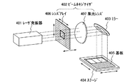
次に図5を用いて、本発明のレーザ照射装置の、図1(A)とは異なる構成について説明する。図5に示すレーザ照射装置は、パルス発振でレーザ光を出力することができるレーザ発振器401と、レーザ発振器401から発振されたレーザ光が入射するビームホモジナイザ402と、ビームホモジナイザ402から射出したレーザ光を成形したり、光路の向きを変えたりすることができる光学系403と、被処理物(ここでは半導体膜が成膜された基板)405を載置するためのステージ404とが設けられている。 Next, the structure different from FIG. 1A of the laser irradiation apparatus of the present invention will be described with reference to FIG. The laser irradiation apparatus shown in FIG. 5 includes a laser oscillator 401 that can output laser light by pulse oscillation, a beam homogenizer 402 on which the laser light emitted from the laser oscillator 401 is incident, and a laser light emitted from the beam homogenizer 402. And an optical system 403 that can change the direction of the optical path, and a stage 404 on which an object to be processed (here, a substrate on which a semiconductor film is formed) 405 is placed. .
なお、レーザ光を形成したり、光路の向きを変えたりすることができる光学系403として、図5ではミラーを例示しているが、ミラー以外の光学系を用いていても良い。 In addition, although the mirror is illustrated in FIG. 5 as the optical system 403 that can form laser light and change the direction of the optical path, an optical system other than the mirror may be used.
また図5には図示していないが、ステージ404の位置を制御するための手段が、本発明のレーザ照射装置に備えられている。なお図5に示すレーザ照射装置は、レーザ光の照射位置を固定して基板405を移動させる被処理物移動型に相当するが、本発明はこの構成に限定されない。被処理物である基板405を固定してレーザ光の照射位置を移動させる照射系移動型であっても良いし、上記2つの方法を組み合わせていても良い。 Although not shown in FIG. 5, means for controlling the position of the stage 404 is provided in the laser irradiation apparatus of the present invention. Note that the laser irradiation apparatus illustrated in FIG. 5 corresponds to a workpiece moving type in which the irradiation position of the laser light is fixed and the substrate 405 is moved, but the present invention is not limited to this structure. An irradiation system moving type in which the substrate 405 as an object to be processed is fixed and the irradiation position of the laser light is moved may be used, or the above two methods may be combined.
ビームホモジナイザ402は、複数の凸レンズを有するレンズアレイ406と、レンズアレイ406の各凸レンズから射出したレーザ光を成形するための集光レンズ407とを有している。なお図5では集光レンズ407を1つだけ用いているが、集光レンズ407を複数用いていても良い。そして図5には図示してはいないが、本発明のレーザ照射装置はレンズアレイ406の位置を制御する位置制御手段を有している。レンズアレイ406の位置を制御することで、レンズアレイ406におけるレーザ光の入射位置を、制御することができる。
The beam homogenizer 402 includes a
なお図5では、レンズアレイ406を、レーザ光の入射方向と垂直な面に対して、上下左右で平行移動させることで、レンズアレイ406に入射するレーザ光の位置を制御しているが、本発明はこの構成に限定されない。例えば、レーザ光の入射方向と平行な軸の方向にレンズアレイ406を前後させても良い。また、レーザ発振器401を平行移動する位置制御装置を備えていてもよい。
In FIG. 5, the position of the laser light incident on the
図6(A)、図6(B)に、レンズアレイ406とレーザ光の入射位置の関係と、各入射位置に対するエリア410でのエネルギー分布を示す。
6A and 6B show the relationship between the
図6(A)、図6(B)に示すように、レンズアレイ406に入射したレーザ光は、レンズアレイ406が有する複数のレンズによって分割された後、集光レンズ407によってエリア410に集光される。そして、レンズアレイ406が有する任意のレンズ408に注目すると、任意のレンズ408に入射するレーザ光は、レンズアレイ406の位置を図6(A)から図6(B)に移動させることで変化する。よって、レンズアレイ406に入射するレーザ光にエネルギー分布が存在している場合、レンズアレイ406の位置を図6(A)から図6(B)に移動させることで、エリア410に集光されたレーザ光のエネルギー分布に変化が生じる。
As shown in FIGS. 6A and 6B, the laser light incident on the
任意のレンズ408に入射するレーザ光の変化を分かりやすくするために、図7(A)、図7(B)に、レーザ光の入射方向から見た、レンズアレイ406とレーザ光の入射位置409との関係を示す。なお図7(A)と図7(B)とでは、レンズアレイ406におけるレーザ光の入射位置409が異なっている。図7(A)、図7(B)に示すように、レーザ光の入射位置409におけるレーザ光にエネルギー分布が存在していると仮定する。この場合、任意のレンズ408に注目すると、図7(A)と図7(B)とでは、レンズ408に入射するレーザ光のエネルギー分布が異なっていることがわかる。よって、図7(A)と図7(B)とでは、ビームホモジナイザから射出されるレーザ光の、エネルギー分布が異なることになる。
7A and 7B, the
従って、空間的なエネルギー分布が異なるパルスを、同一領域に重ねて照射することで、エネルギー分布を均一化させることができ、均一なレーザアニールを行なうことが可能になる。 Therefore, by irradiating the same region with pulses having different spatial energy distributions, the energy distribution can be made uniform and uniform laser annealing can be performed.
なお本発明のレーザ照射装置は、図1(A)に示したレーザ照射装置にさらにビームホモジナイザを設けていても良い。そして該ビームホモジナイザは、図5に示した構成を有していても良い。図11に、図1(A)に示した構成と、図5に示した構成を組み合わせた、本発明のレーザ照射装置の構成を示す。 Note that the laser irradiation apparatus of the present invention may further include a beam homogenizer in the laser irradiation apparatus illustrated in FIG. The beam homogenizer may have the configuration shown in FIG. FIG. 11 shows a structure of the laser irradiation apparatus of the present invention, which is a combination of the structure shown in FIG. 1A and the structure shown in FIG.
図11に示すレーザ照射装置は、パルス発振でレーザ光を出力することができるレーザ発振器601と、レーザ発振器601から発振されたレーザ光のうち、選択されたパルスの面内における空間的なエネルギー分布を反転または回転させることができる光学系(レンズアッセンブリ)602と、レンズアッセンブリ602から射出したレーザ光が入射するビームホモジナイザ603と、ビームホモジナイザ603から射出したレーザ光を成形したり、光路の向きを変えたりすることができる光学系(ここではミラーを例示)604と、被処理物(ここでは半導体膜が成膜された基板)606を載置するためのステージ605とが設けられている。
The laser irradiation apparatus shown in FIG. 11 has a
また図11には図示していないが、ステージ605の位置を制御するための手段が、本発明のレーザ照射装置に備えられている。なお図11に示すレーザ照射装置は、レーザ光の照射位置を固定して基板606を移動させる被処理物移動型に相当するが、本発明はこの構成に限定されない。被処理物である基板606を固定してレーザ光の照射位置を移動させる照射系移動型であっても良いし、上記2つの方法を組み合わせていても良い。
Although not shown in FIG. 11, means for controlling the position of the
図1(A)と同様に、レンズアッセンブリ602には、レーザ光のエネルギー分布を反転または回転させるための、複数の光学系が設けられている。レンズアッセンブリ602を回転させることで、入射するレーザ光の位置を制御し、複数の光学系のいずれか1組を選択する。図11には図示していないが、本発明のレーザ照射装置は、レンズアッセンブリ602に入射するレーザ光の位置を制御する位置制御手段を備えている。レンズアッセンブリ602から選択された光学系が、レーザ光の照射面におけるエネルギー分布を制御する。 As in FIG. 1A, the lens assembly 602 is provided with a plurality of optical systems for reversing or rotating the energy distribution of the laser light. By rotating the lens assembly 602, the position of the incident laser beam is controlled, and any one of a plurality of optical systems is selected. Although not shown in FIG. 11, the laser irradiation apparatus of the present invention includes position control means for controlling the position of the laser light incident on the lens assembly 602. The optical system selected from the lens assembly 602 controls the energy distribution on the laser light irradiation surface.
なお、図11ではレンズアッセンブリ602に入射するレーザ光の位置を、レンズアッセンブリ602を回転させることで制御しているが、本発明はこの構成に限定されない。レーザ光の周波数に同期して、複数の光学系を選択することができれば良い。例えば、レーザ発振器601を平行移動する位置制御装置を備えていてもよい。
In FIG. 11, the position of the laser beam incident on the lens assembly 602 is controlled by rotating the lens assembly 602, but the present invention is not limited to this configuration. It is sufficient that a plurality of optical systems can be selected in synchronization with the frequency of the laser beam. For example, a position control device that translates the
ビームホモジナイザ603は、複数の凸レンズを有するレンズアレイ607と、レンズアレイ607の各凸レンズから射出したレーザ光を同一領域に照射するための集光レンズ608とを有している。なお図11では集光レンズ608を1つだけ用いているが、集光レンズ608を複数用いていても良い。そして図11には図示してはいないが、本発明のレーザ照射装置はレンズアレイ607の位置を制御する位置制御手段を有している。レンズアレイ607の位置を制御することで、レンズアレイ607におけるレーザ光の入射位置を、制御することができる。
The
なお図11では、レンズアレイ607を、レーザ光の入射方向と垂直な面に対して、上下左右で平行移動させることで、レンズアレイ607に入射するレーザ光の位置を制御しているが、本発明はこの構成に限定されない。例えば、レーザ光の入射方向と平行な軸の方向にレンズアレイ607を前後させても良い。また、レーザ発振器601の位置を制御する位置制御装置を備えていても良い。
In FIG. 11, the position of the laser light incident on the lens array 607 is controlled by translating the lens array 607 vertically and horizontally with respect to a plane perpendicular to the incident direction of the laser light. The invention is not limited to this configuration. For example, the lens array 607 may be moved back and forth in the direction of an axis parallel to the incident direction of the laser light. Further, a position control device that controls the position of the
図11に示すように、図1(A)と図5の構成を組み合わせることで、同一領域に照射されるレーザ光のトータルのエネルギー分布を、より平均化することができる。 As shown in FIG. 11, the total energy distribution of the laser light applied to the same region can be further averaged by combining the configurations of FIG. 1A and FIG. 5.
本実施例では、本発明のレーザ照射装置を用いた半導体膜の作製方法について、具体的に説明する。 In this embodiment, a method for manufacturing a semiconductor film using the laser irradiation apparatus of the present invention will be specifically described.
まず図8(A)に示すように、基板500上に下地膜501を成膜する。基板500には、例えばバリウムホウケイ酸ガラスや、アルミノホウケイ酸ガラスなどのガラス基板、石英基板、SUS基板等を用いることができる。また、プラスチック等の可撓性を有する合成樹脂からなる基板は、一般的に上記基板と比較して耐熱温度が低い傾向にあるが、作製工程における処理温度に耐え得るのであれば用いることが可能である。
First, as shown in FIG. 8A, a
下地膜501は基板500中に含まれるNaなどのアルカリ金属やアルカリ土類金属が、半導体膜中に拡散し、半導体素子の特性に悪影響を及ぼすのを防ぐために設ける。よってアルカリ金属やアルカリ土類金属の半導体膜への拡散を抑えることができる酸化珪素や、窒化珪素、窒化酸化珪素などの絶縁膜を用いて形成する。本実施例では、プラズマCVD法を用いて窒化酸化珪素膜を10〜400nm(好ましくは50〜300nm)の膜厚になるように成膜する。
The
なお下地膜501は単層であっても複数の絶縁膜を積層したものであっても良い。またガラス基板、SUS基板またはプラスチック基板のように、アルカリ金属やアルカリ土類金属が多少なりとも含まれている基板を用いる場合、不純物の拡散を防ぐという観点から下地膜を設けることは有効であるが、石英基板など不純物の拡散がさして問題とならない場合は、必ずしも設ける必要はない。
Note that the
次に下地膜上に半導体膜502を形成する。半導体膜502の膜厚は25〜100nm(好ましくは30〜60nm)とする。なお半導体膜502は、非晶質半導体であっても良いし、多結晶半導体であっても良い。また半導体は珪素だけではなくシリコンゲルマニウムも用いることができる。シリコンゲルマニウムを用いる場合、ゲルマニウムの濃度は0.01〜4.5atomic%程度であることが好ましい。
Next, a
次に図8(B)に示すように、半導体膜502を本発明のレーザ照射装置を用いて結晶化する。本発明において、レーザは、公知のパルス発振の気体レーザもしくは固体レーザを用いることができる。例えば、Cr、Nd、Er、Ho、Ce、Co、Ti又はTmがドーピングされたYAGレーザ、YVO4レーザ、YLFレーザ、YAlO3レーザ、GdVO4レーザ、ガラスレーザ、ルビーレーザ、アレキサンドライドレーザ、Ti:サファイアレーザなどがある。当該レーザの基本波はドーピングする材料によって異なるが、1μm前後の基本波を有するレーザ光が得られる。基本波に対する第2高調波、第3高調波および第4高調波は、非線形光学素子を用いることで得ることができる。
Next, as shown in FIG. 8B, the
本実施例では、波長308nmのレーザ光を、1パルスで数cm2〜数十cm2(本実施例では例えば3×5cm2)の領域に照射することができるエキシマレーザ(ソプラ社製)を用いる。そして、該ビームスポットにおけるエネルギー密度を400〜900mJ/cm2(本実施例では600mJ/cm2)、パルス幅170ns、発振周波数1〜30Hz(本実施例では20Hz)とし、任意の領域に数パルス(本実施例では4パルス)ずつレーザ光を照射する。
In this embodiment, an excimer laser (manufactured by Sopra) capable of irradiating a laser beam having a wavelength of 308 nm to a region of several cm 2 to several tens of cm 2 (in this embodiment, for example, 3 × 5 cm 2 ) by one pulse. Use. Then, (600 mJ / cm 2 in this embodiment) the energy density 400~900mJ / cm 2 in the beam spot, the pulse width 170 ns, and the
また本発明では、任意の領域に照射される複数のパルスのうち、少なくとも1つのパルスが、他のパルスとエネルギー分布が異なるようにする。上記構成により、トータルのエネルギー分布が均一化され、半導体膜の結晶性をより均一化させることができる。 In the present invention, at least one pulse among a plurality of pulses irradiated to an arbitrary region is made different in energy distribution from other pulses. With the above structure, the total energy distribution is made uniform, and the crystallinity of the semiconductor film can be made more uniform.
上述した半導体膜502へのレーザ光の照射により、結晶性がより高められた半導体膜503が形成される。
By irradiating the
次に、図8(C)に示すように半導体膜503をパターニングし、島状の半導体膜504〜506が形成される。そして、該島状の半導体膜504〜506を用いて、図8(D)に示すようにTFT507〜509を形成することで、TFTの特性、例えばオン電流、移動度等のばらつきを抑えることができる。
Next, as illustrated in FIG. 8C, the
また、半導体表示装置の画素部全体をカバーできる程度にビームスポットのサイズを広げることで、レーザ光の各パルス間で生じる数%のエネルギーの揺らぎに起因する輝度むらが、視認されるのを抑えることができる。 Further, by expanding the size of the beam spot to the extent that the entire pixel portion of the semiconductor display device can be covered, it is possible to prevent the luminance unevenness caused by the fluctuation of several percent of energy generated between each pulse of the laser light from being visually recognized. be able to.
本実施例では、互いにエネルギー分布が異なる複数のパルスを、被処理物に照射する順番について説明する。 In the present embodiment, the order of irradiating a workpiece with a plurality of pulses having different energy distributions will be described.
まず図9(A)に示すように、被処理物の各領域に、1パルス目のレーザ光が矢印の順に照射されると仮定する。次に図9(B)に示すように、被処理物の各領域に、2パルス目のレーザ光が矢印の順に照射される。そして図9(C)に示すように、被処理物の各領域に、3パルス目のレーザ光が矢印の順に照射され、次に、図9(D)に示すように、被処理物の各領域に、4パルス目のレーザ光が矢印の順に照射される。 First, as shown in FIG. 9A, it is assumed that each region of the workpiece is irradiated with the first pulse of laser light in the order of the arrows. Next, as shown in FIG. 9B, each region of the workpiece is irradiated with the second pulse of laser light in the order of the arrows. Then, as shown in FIG. 9C, each region of the object to be processed is irradiated with the laser light of the third pulse in the order of the arrows, and then, as shown in FIG. The region is irradiated with the fourth pulse of laser light in the order of the arrows.
そして、2パルス目から4パルス目のレーザ光の照射も、1パルス目と同様に、隣り合うエリアに対応するパルスが、互いに異なるエネルギー分布を有するようにする。 In addition, similarly to the first pulse, the second to fourth laser light irradiation is performed so that pulses corresponding to adjacent areas have different energy distributions.
なお本実施例では、各領域に4パルスのレーザ光を照射する例を示しているが、同一領域に照射するパルスの数はこれに限定されず、複数であれば良い。 In the present embodiment, an example in which each region is irradiated with four pulses of laser light is shown. However, the number of pulses irradiated to the same region is not limited to this and may be plural.
本実施例では、互いにエネルギー分布が異なる複数のパルスを、被処理物に照射する順番について説明する。 In the present embodiment, the order of irradiating a workpiece with a plurality of pulses having different energy distributions will be described.
まず図10(A)に示すように、被処理物の各領域に、1パルス目のレーザ光が矢印の順に照射されると仮定する。なお図10(A)では、隣り合うエリアに対応するパルスは、互いにエネルギー分布が同じである。 First, as shown in FIG. 10A, it is assumed that each region of the object to be processed is irradiated with the first pulse of laser light in the order of the arrows. In FIG. 10A, pulses corresponding to adjacent areas have the same energy distribution.
次に図10(B)に示すように、被処理物の各領域に、2パルス目のレーザ光が矢印の順に照射される。そして図10(C)に示すように、被処理物の各領域に、3パルス目のレーザ光が矢印の順に照射され、次に、図10(D)に示すように、被処理物の各領域に、4パルス目のレーザ光が矢印の順に照射される。 Next, as shown in FIG. 10B, each region of the object to be processed is irradiated with the second pulse of laser light in the order of the arrows. Then, as shown in FIG. 10C, each region of the object to be processed is irradiated with the laser light of the third pulse in the order of the arrows, and then, as shown in FIG. The region is irradiated with the fourth pulse of laser light in the order of the arrows.
なお本実施例では、各領域に4パルスのレーザ光を照射する例を示しているが、同一領域に照射するパルスの数はこれに限定されず、複数であれば良い。 In the present embodiment, an example in which each region is irradiated with four pulses of laser light is shown. However, the number of pulses irradiated to the same region is not limited to this and may be plural.
本実施例では図10(A)〜図10(D)に示すように、各領域に照射される複数のパルスは、互いにそのエネルギー分布が異なっている。そして本実施例では、同一の領域に連続して全てのパルスを照射するのではなく、1つのパルスが照射された後、他のエリアへのパルスの照射を行ない、再び次のパルスを照射している。本実施例に示す順番でレーザ光を照射することで、レンズアッセンブリの位置を制御する手段やレンズアレイの位置を制御するための手段の動作周波数を、実施例2の場合に比べて抑えることができるというメリットが得られる。 In this embodiment, as shown in FIGS. 10A to 10D, energy distributions of a plurality of pulses irradiated to the respective regions are different from each other. In this embodiment, instead of continuously irradiating the same region with all the pulses, after one pulse is irradiated, the other area is irradiated with a pulse, and the next pulse is irradiated again. ing. By irradiating the laser beams in the order shown in the present embodiment, the operating frequency of the means for controlling the position of the lens assembly and the means for controlling the position of the lens array can be suppressed as compared with the case of the second embodiment. The advantage that you can do it.
101 レーザ発振器
102 レンズアッセンブリ
103 光学系
104 ステージ
105 基板
110 光学系
111 光学系
112 光学系
113 光学系
201 シリンドリカルレンズ
202 シリンドリカルレンズ
203 シリンドリカルレンズ
204 シリンドリカルレンズ
205 平凸球面レンズ
206 平凸球面レンズ
301 凸レンズ
302 凸レンズ
303 凸レンズ
304 凸レンズ
305 凸レンズ
306 凸レンズ
307 凸レンズ
308 凸レンズ
401 レーザ発振器
402 ビームホモジナイザ
403 光学系
404 ステージ
405 基板
406 レンズアレイ
407 集光レンズ
408 レンズ
409 入射位置
410 エリア
500 基板
501 下地膜
502 半導体膜
503 半導体膜
504 島状の半導体膜
505 島状の半導体膜
506 島状の半導体膜
507 TFT
508 TFT
509 TFT
601 レーザ発振器
602 レンズアッセンブリ
603 ビームホモジナイザ
604 ミラー
605 ステージ
606 基板
607 レンズアレイ
608 集光レンズ
DESCRIPTION OF SYMBOLS 101 Laser oscillator 102 Lens assembly 103 Optical system 104 Stage 105
508 TFT
509 TFT
601 Laser oscillator 602
Claims (5)
複数の光学系を有するレンズアッセンブリと、
前記パルス発振と同期して前記レンズアッセンブリの位置を制御することによって、前記複数の光学系から少なくとも第1の光学系又は第2の光学系を選択する位置制御手段とを有し、
前記第1の光学系における前記レーザ光の空間的なエネルギー分布の反転の軸と、前記第2の光学系における前記レーザ光の空間的なエネルギー分布の反転の軸が、互いに交差することを特徴とするレーザ照射装置。 A laser oscillator that outputs laser light by pulse oscillation;
A lens assembly having a plurality of optical systems;
Position control means for selecting at least the first optical system or the second optical system from the plurality of optical systems by controlling the position of the lens assembly in synchronization with the pulse oscillation;
Said the inversion of the axis of the first spatial energy distribution of the laser beam in the optical system of the inversion of the axis of the spatial energy distribution of the laser beam in the second optical system intersect each other The laser irradiation apparatus characterized by this.
複数の光学系を有するレンズアッセンブリと、
前記パルス発振と同期して前記レンズアッセンブリの位置を制御することによって、前記複数の光学系から少なくとも第1の光学系又は第2の光学系を選択する第1の位置制御手段と、
レンズアレイ及び集光レンズを有するビームホモジナイザと、
前記レンズアレイの位置を前記レーザ光の入射方向に垂直な平面上で、又は前記レーザ光の入射方向と平行な軸上で平行移動するように制御する第2の位置制御手段とを有し、
前記第1の光学系における前記レーザ光の空間的なエネルギー分布の反転の軸と、前記第2の光学系における前記レーザ光の空間的なエネルギー分布の反転の軸が、互いに交差することを特徴とするレーザ照射装置。 A laser oscillator that outputs laser light by pulse oscillation;
A lens assembly having a plurality of optical systems;
First position control means for selecting at least the first optical system or the second optical system from the plurality of optical systems by controlling the position of the lens assembly in synchronization with the pulse oscillation;
A beam homogenizer having a lens array and a condenser lens;
Second position control means for controlling the position of the lens array to translate on a plane perpendicular to the incident direction of the laser beam or on an axis parallel to the incident direction of the laser beam;
Said the inversion of the axis of the first spatial energy distribution of the laser beam in the optical system of the inversion of the axis of the spatial energy distribution of the laser beam in the second optical system intersect each other The laser irradiation apparatus characterized by this.
前記パルス発振に同期して、複数の光学系を有するレンズアッセンブリの位置を制御することによって、前記複数の光学系のうち少なくとも2つの光学系が選択され、
前記選択された少なくとも2つの光学系によって、レーザ光の空間的なエネルギー分布が互いに反転した複数のパルスを形成し、
前記複数のパルスを、半導体膜の同一領域に照射することを特徴とする半導体装置の作製方法。 Laser light is output by pulse oscillation,
By controlling the position of a lens assembly having a plurality of optical systems in synchronization with the pulse oscillation, at least two optical systems are selected from the plurality of optical systems,
By at least two optical systems the selected, to form a plurality of pulses where the spatial energy distribution of the laser light is inverted with each other,
A method for manufacturing a semiconductor device, wherein the plurality of pulses are applied to the same region of a semiconductor film.
前記パルス発振に同期して、複数の光学系を有するレンズアッセンブリの位置を制御することによって、前記複数の光学系のうち少なくとも第1の光学系及び第2の光学系が選択され、
前記第1の光学系により第1の直線を軸としてレーザ光の空間的なエネルギー分布が互いに反転した第1のパルスを形成し、
前記第2の光学系により前記第1の直線と交差する第2の直線を軸としてレーザ光の空間的なエネルギー分布が互いに反転した第2のパルスを形成し、
前記第1のパルスと前記第2のパルスを含む複数のパルスを、半導体膜の同一領域に照射することを特徴とする半導体装置の作製方法。 Laser light is output by pulse oscillation,
By controlling the position of a lens assembly having a plurality of optical systems in synchronization with the pulse oscillation, at least a first optical system and a second optical system are selected from among the plurality of optical systems,
Wherein the first optical system spatial energy distribution of the laser beam to form a first pulse that is inverted with each other a first straight line as an axis,
The spatial energy distribution of the laser beam to form a second pulses inverted to each other a second straight line intersecting the first straight line as an axis by the second optical system,
A method for manufacturing a semiconductor device, wherein the same region of a semiconductor film is irradiated with a plurality of pulses including the first pulse and the second pulse.
前記パルス発振に同期して、複数の光学系を有するレンズアッセンブリの位置を制御することによって、前記複数の光学系のうち少なくとも第1の光学系及び第2の光学系が選択され、
前記第1の光学系により第1の直線を軸としてレーザ光の空間的なエネルギー分布が互いに反転した第1のパルスを形成し、
前記第2の光学系により前記第1の直線と交差する第2の直線を軸としてレーザ光の空間的なエネルギー分布が互いに反転した第2のパルスを形成し、
前記パルス発振に同期してビームホモジナイザが有するレンズアレイの位置を前記レーザ光の入射方向に垂直な平面上で、又は前記レーザ光の入射方向と平行な軸上で平行移動させて制御することによって、前記第1のパルス又は前記第2のパルスが前記レンズアレイに入射する位置が選択され、
前記第1のパルスが前記レンズアレイに入射する位置によってレーザ光の空間的なエネルギー分布が互いに異なる、第3のパルスを前記ビームホモジナイザで形成し、
前記第2のパルスが前記レンズアレイに入射する位置によってレーザ光の空間的なエネルギー分布が互いに異なる、第4のパルスを前記ビームホモジナイザで形成し、
前記第3のパルス及び前記第4のパルスを含む複数のパルスを、半導体膜の同一領域に照射することを特徴とする半導体装置の作製方法。 Laser light is output by pulse oscillation,
By controlling the position of a lens assembly having a plurality of optical systems in synchronization with the pulse oscillation, at least a first optical system and a second optical system are selected from among the plurality of optical systems,
Wherein the first optical system spatial energy distribution of the laser beam to form a first pulse that is inverted with each other a first straight line as an axis,
The spatial energy distribution of the laser beam to form a second pulses inverted to each other a second straight line intersecting the first straight line as an axis by the second optical system,
By controlling the position of the lens array of the beam homogenizer in parallel with the pulse oscillation on a plane perpendicular to the incident direction of the laser beam or on an axis parallel to the incident direction of the laser beam. A position at which the first pulse or the second pulse is incident on the lens array is selected;
Forming a third pulse by the beam homogenizer, the spatial energy distribution of the laser light being different from each other depending on the position where the first pulse is incident on the lens array;
Forming a fourth pulse with the beam homogenizer, the spatial energy distribution of the laser light being different from each other depending on the position where the second pulse is incident on the lens array;
A method for manufacturing a semiconductor device, wherein the same region of a semiconductor film is irradiated with a plurality of pulses including the third pulse and the fourth pulse.
Priority Applications (1)
| Application Number | Priority Date | Filing Date | Title |
|---|---|---|---|
| JP2004261235A JP4780943B2 (en) | 2003-09-09 | 2004-09-08 | Laser irradiation apparatus and method for manufacturing semiconductor device |
Applications Claiming Priority (3)
| Application Number | Priority Date | Filing Date | Title |
|---|---|---|---|
| JP2003317049 | 2003-09-09 | ||
| JP2003317049 | 2003-09-09 | ||
| JP2004261235A JP4780943B2 (en) | 2003-09-09 | 2004-09-08 | Laser irradiation apparatus and method for manufacturing semiconductor device |
Publications (3)
| Publication Number | Publication Date |
|---|---|
| JP2005109460A JP2005109460A (en) | 2005-04-21 |
| JP2005109460A5 JP2005109460A5 (en) | 2007-10-25 |
| JP4780943B2 true JP4780943B2 (en) | 2011-09-28 |
Family
ID=34554226
Family Applications (1)
| Application Number | Title | Priority Date | Filing Date |
|---|---|---|---|
| JP2004261235A Expired - Fee Related JP4780943B2 (en) | 2003-09-09 | 2004-09-08 | Laser irradiation apparatus and method for manufacturing semiconductor device |
Country Status (1)
| Country | Link |
|---|---|
| JP (1) | JP4780943B2 (en) |
Families Citing this family (4)
| Publication number | Priority date | Publication date | Assignee | Title |
|---|---|---|---|---|
| KR100956339B1 (en) | 2003-02-25 | 2010-05-06 | 삼성전자주식회사 | Crystallization system of silicon and crystallization method of silicon |
| CN101911256B (en) | 2008-01-07 | 2012-07-18 | 株式会社Ihi | Laser anneal method and device |
| US8115137B2 (en) | 2008-06-12 | 2012-02-14 | Ihi Corporation | Laser annealing method and laser annealing apparatus |
| WO2019123612A1 (en) * | 2017-12-21 | 2019-06-27 | ギガフォトン株式会社 | Laser irradiation system |
Family Cites Families (8)
| Publication number | Priority date | Publication date | Assignee | Title |
|---|---|---|---|---|
| JPH01179908A (en) * | 1988-01-11 | 1989-07-18 | Fujitsu Ltd | Method for uniformizing intensity distribution of laser beam |
| JP3116465B2 (en) * | 1991-10-04 | 2000-12-11 | ソニー株式会社 | Excimer laser light irradiation device |
| JPH10256179A (en) * | 1997-03-10 | 1998-09-25 | Semiconductor Energy Lab Co Ltd | Device and method for laser light irradiation |
| JP4403599B2 (en) * | 1999-04-19 | 2010-01-27 | ソニー株式会社 | Semiconductor thin film crystallization method, laser irradiation apparatus, thin film transistor manufacturing method, and display apparatus manufacturing method |
| JP2001028346A (en) * | 1999-07-14 | 2001-01-30 | Sumitomo Heavy Ind Ltd | Shutter mechanism for precise irradiation and control method |
| JP2001257174A (en) * | 2000-03-13 | 2001-09-21 | Sumitomo Heavy Ind Ltd | Laser annealing device and method |
| JP4827305B2 (en) * | 2001-03-16 | 2011-11-30 | 株式会社半導体エネルギー研究所 | Method for manufacturing semiconductor device |
| KR100379361B1 (en) * | 2001-05-30 | 2003-04-07 | 엘지.필립스 엘시디 주식회사 | crystallization method of a silicon film |
-
2004
- 2004-09-08 JP JP2004261235A patent/JP4780943B2/en not_active Expired - Fee Related
Also Published As
| Publication number | Publication date |
|---|---|
| JP2005109460A (en) | 2005-04-21 |
Similar Documents
| Publication | Publication Date | Title |
|---|---|---|
| KR101268107B1 (en) | Laser irradiation apparatus, laser irradiation method, and method for manufacturing a semiconductor device | |
| JP4838982B2 (en) | Laser annealing method and laser annealing apparatus | |
| KR100626772B1 (en) | Laser annealing apparatus | |
| JP4413569B2 (en) | Display panel manufacturing method and display panel | |
| US6563843B1 (en) | Laser irradiation device | |
| US7566669B2 (en) | Laser irradiation apparatus and laser irradiation method | |
| KR101017848B1 (en) | Beam homogenizer and laser irradiation apparatus and method of manufacturing semiconductor device | |
| US20010043401A1 (en) | Laser optical apparatus | |
| US20040069751A1 (en) | Method of irradiating laser, laser irradiation system, and manufacturing method of semiconductor device | |
| US7919726B2 (en) | Laser irradiation apparatus, laser irradiation method, and method for manufacturing a semiconductor device | |
| JPWO2009087784A1 (en) | Laser annealing method and apparatus | |
| JPH05226790A (en) | Laser annealer | |
| JP2004103628A (en) | Laser annealing device and method of laser-annealing tft substrate | |
| US7387922B2 (en) | Laser irradiation method, method for manufacturing semiconductor device, and laser irradiation system | |
| JP4780943B2 (en) | Laser irradiation apparatus and method for manufacturing semiconductor device | |
| JP3029787B2 (en) | Laser annealing method and liquid crystal display device manufacturing method | |
| JP4628879B2 (en) | Manufacturing method of display device | |
| JP4799825B2 (en) | Laser irradiation method | |
| JP2003332258A (en) | Laser annealing device, semiconductor device and method of manufacturing semiconductor device | |
| JP4619035B2 (en) | Beam homogenizer, laser irradiation apparatus, and method for manufacturing semiconductor device | |
| JP4969024B2 (en) | Method for manufacturing semiconductor device | |
| JP2004134785A (en) | Beam homogenizer, laser irradiator and method for manufacturing semiconductor device | |
| WO2020184153A1 (en) | Laser annealing device | |
| KR20220036414A (en) | Laser irradiaion apparatus and laser irradiation method | |
| KR20050121548A (en) | Method for crystallizing silicon and method of manufacturing tft substrate using the same |
Legal Events
| Date | Code | Title | Description |
|---|---|---|---|
| A521 | Written amendment |
Free format text: JAPANESE INTERMEDIATE CODE: A523 Effective date: 20070907 |
|
| A621 | Written request for application examination |
Free format text: JAPANESE INTERMEDIATE CODE: A621 Effective date: 20070907 |
|
| A977 | Report on retrieval |
Free format text: JAPANESE INTERMEDIATE CODE: A971007 Effective date: 20101125 |
|
| A131 | Notification of reasons for refusal |
Free format text: JAPANESE INTERMEDIATE CODE: A131 Effective date: 20101130 |
|
| A521 | Written amendment |
Free format text: JAPANESE INTERMEDIATE CODE: A523 Effective date: 20101207 |
|
| TRDD | Decision of grant or rejection written | ||
| A01 | Written decision to grant a patent or to grant a registration (utility model) |
Free format text: JAPANESE INTERMEDIATE CODE: A01 Effective date: 20110628 |
|
| A01 | Written decision to grant a patent or to grant a registration (utility model) |
Free format text: JAPANESE INTERMEDIATE CODE: A01 |
|
| A61 | First payment of annual fees (during grant procedure) |
Free format text: JAPANESE INTERMEDIATE CODE: A61 Effective date: 20110705 |
|
| FPAY | Renewal fee payment (event date is renewal date of database) |
Free format text: PAYMENT UNTIL: 20140715 Year of fee payment: 3 |
|
| R150 | Certificate of patent or registration of utility model |
Free format text: JAPANESE INTERMEDIATE CODE: R150 |
|
| FPAY | Renewal fee payment (event date is renewal date of database) |
Free format text: PAYMENT UNTIL: 20140715 Year of fee payment: 3 |
|
| R250 | Receipt of annual fees |
Free format text: JAPANESE INTERMEDIATE CODE: R250 |
|
| R250 | Receipt of annual fees |
Free format text: JAPANESE INTERMEDIATE CODE: R250 |
|
| R250 | Receipt of annual fees |
Free format text: JAPANESE INTERMEDIATE CODE: R250 |
|
| R250 | Receipt of annual fees |
Free format text: JAPANESE INTERMEDIATE CODE: R250 |
|
| LAPS | Cancellation because of no payment of annual fees |