JP4765852B2 - Electro-optical device and electronic apparatus - Google Patents
Electro-optical device and electronic apparatus Download PDFInfo
- Publication number
- JP4765852B2 JP4765852B2 JP2006243743A JP2006243743A JP4765852B2 JP 4765852 B2 JP4765852 B2 JP 4765852B2 JP 2006243743 A JP2006243743 A JP 2006243743A JP 2006243743 A JP2006243743 A JP 2006243743A JP 4765852 B2 JP4765852 B2 JP 4765852B2
- Authority
- JP
- Japan
- Prior art keywords
- photosensor
- optical sensor
- elements
- electro
- sensor element
- Prior art date
- Legal status (The legal status is an assumption and is not a legal conclusion. Google has not performed a legal analysis and makes no representation as to the accuracy of the status listed.)
- Active
Links
Images


Classifications
-
- Y—GENERAL TAGGING OF NEW TECHNOLOGICAL DEVELOPMENTS; GENERAL TAGGING OF CROSS-SECTIONAL TECHNOLOGIES SPANNING OVER SEVERAL SECTIONS OF THE IPC; TECHNICAL SUBJECTS COVERED BY FORMER USPC CROSS-REFERENCE ART COLLECTIONS [XRACs] AND DIGESTS
- Y02—TECHNOLOGIES OR APPLICATIONS FOR MITIGATION OR ADAPTATION AGAINST CLIMATE CHANGE
- Y02B—CLIMATE CHANGE MITIGATION TECHNOLOGIES RELATED TO BUILDINGS, e.g. HOUSING, HOUSE APPLIANCES OR RELATED END-USER APPLICATIONS
- Y02B20/00—Energy efficient lighting technologies, e.g. halogen lamps or gas discharge lamps
- Y02B20/40—Control techniques providing energy savings, e.g. smart controller or presence detection
Description
本発明は、外光照度を光センサ素子にて検出し、その検出値を用いてバックライト輝度等を自動的に調整する電気光学装置及び電子機器において、光センサ素子を使用して光センサ素子が劣化した場合でも、別の光センサ素子に切り替えて長期間に亘って継続して外光検出を行えるようにした電気光学装置及び電子機器に関する。 The present invention relates to an electro-optical device and an electronic apparatus that detect external light illuminance with a light sensor element, and automatically adjust backlight luminance or the like using the detected value. The present invention relates to an electro-optical device and an electronic apparatus that can detect ambient light continuously over a long period of time by switching to another optical sensor element even when the sensor is deteriorated.
液晶装置等の電気光学装置においては、暗所における画像を見易くしたりバックライトの消費電力を抑える目的で、周囲の明るさに応じてバックライト輝度を調整する手段が用いられる。
例えば特許文献1のように液晶パネル内に光センサを搭載して外光を検出し、液晶表示装置のバックライト発光量の調整を行うバックライト制御技術が近年開発されている。これはパネル内に光センサを作り込むため部品点数を減らせ、携帯電話機等のメーカーでの製造時の負荷を軽減しかつデザインの自由度を上げることができる。また、特許文献2のように液晶表示装置に複数の光センサを備え、これらのセンサで検出した外光照度データの平均値を算出し、その結果に応じてバックライトを調光する方法もある。
For example, as in
しかしながら、上記の特許文献1,2の構成では、表示装置に設けた光センサには常に外光が入射し照射する光により光センサは劣化していくため、所望の感度を長期に亘って維持するのは困難となる。
そこで、本発明は、上記の問題に鑑み、長期間に亘って光センサによる照度検出を所望の感度を保って継続することができる光センサ付きの電気光学装置及び電子機器を提供することを目的とするものである。
However, in the configurations of the above-mentioned
SUMMARY OF THE INVENTION In view of the above problems, an object of the present invention is to provide an electro-optical device and an electronic apparatus with an optical sensor that can continue illuminance detection by an optical sensor with a desired sensitivity over a long period of time. It is what.
本発明による電気光学装置は、複数の走査線と複数のデータ線との交差に対応して画素電極を有する素子基板と、当該素子基板と対向して配置される対向電極を有する対向基板との間に電気光学物質が挟持されて表示領域が形成される電気光学装置において、前記対向基板上に偏光板が配置され、前記素子基板上に形成され、外光の照度を検出する光センサ部と、該光センサ部の上に形成された偏光部と、該偏光部の上に形成された透明電極と、前記光センサ部における複数の光センサ素子とこれらの光センサ素子の中から少なくとも1つを使用する光センサ素子として選択する選択手段とを具備し、 前記光センサ部の上部の前記透明電極を電気的に制御することによって、該光センサ部を遮光可能としたことを特徴とする。
An electro-optical device according to the present invention includes an element substrate having a pixel electrode corresponding to the intersection of a plurality of scanning lines and a plurality of data lines, and a counter substrate having a counter electrode disposed to face the element substrate. In an electro-optical device in which a display region is formed with an electro-optical material interposed therebetween, a polarizing plate is disposed on the counter substrate, and is formed on the element substrate, and an optical sensor unit that detects the illuminance of external light A polarizing part formed on the optical sensor part, a transparent electrode formed on the polarizing part, a plurality of optical sensor elements in the optical sensor part, and at least one of these optical sensor elements Selection means for selecting the light sensor element to be used, and by electrically controlling the transparent electrode above the light sensor part, the light sensor part can be shielded from light.
本発明によるこのような構成によれば、複数の光センサ素子の中から少なくとも1つを使用する光センサ素子として選択可能であると共に、光センサ部の上部の電気光学物質(例えば、液晶)を利用して、未使用時の光センサ素子を遮光できるので、光センサ部の劣化を軽減することができる。 According to such a configuration of the present invention, it is possible to select an optical sensor element that uses at least one of a plurality of optical sensor elements, and an electro-optic material (for example, liquid crystal) on the upper part of the optical sensor unit. By utilizing the light sensor element when not in use, the deterioration of the light sensor unit can be reduced.
本発明において、前記光センサ素子が劣化したか否かを判断し、劣化したことを判断した場合、前記選択手段を制御して別の光センサ素子に切り替える制御部を具備したことを特徴とする。 In the present invention, it is determined whether or not the optical sensor element has deteriorated, and when it is determined that the optical sensor element has deteriorated, a control unit that controls the selection unit to switch to another optical sensor element is provided. .
このような構成によれば、光センサ素子が劣化した場合、新たな光センサ素子に切り替えることで、長期間に亘って光センサ素子による照度検出を所望の感度を保って継続することができる。 According to such a configuration, when the optical sensor element is deteriorated, illuminance detection by the optical sensor element can be continued with a desired sensitivity over a long period of time by switching to a new optical sensor element.
本発明において、前記制御部は、前記複数の光センサ素子のうちの第1の光センサ素子を前記選択手段にて選択するとともに、該第1の光センサ素子における上部の透明電極を電気的に制御して第1の光センサ素子への外光照射を可能とし、前記第1の光センサ素子の使用時間又は使用回数が上限に達した場合、前記選択手段にて使用する次の光センサ素子を選択して前記複数の光センサ素子の最後の光センサ素子まで外光照度検出を継続して実行させることを特徴とする。 In the present invention, the control unit selects a first photosensor element of the plurality of photosensor elements by the selection means, and electrically connects an upper transparent electrode in the first photosensor element. The first photosensor element is controlled to enable external light irradiation, and when the use time or the number of times of use of the first photosensor element reaches the upper limit, the next photosensor element used by the selection means And detecting ambient light illuminance continuously until the last photosensor element of the plurality of photosensor elements.
このような構成によれば、複数の光センサ素子を用意して、1つの光センサ素子が使用不能となる前に、1つの光センサ素子が劣化したことを判断して、次の光センサ素子に切り替えていくので、全ての光センサ素子を順次に使用することになり、長期間に亘って外光をセンシングして電気光学装置のバックライト調光制御等に用いることが可能となる。 According to such a configuration, a plurality of photosensor elements are prepared, and it is determined that one photosensor element has deteriorated before one photosensor element becomes unusable. Therefore, all the optical sensor elements are used sequentially, and it becomes possible to sense external light over a long period of time and use it for backlight dimming control of the electro-optical device.
本発明において、前記制御部は、前記複数の光センサ素子のうちの第1の光センサ素子を前記選択手段にて選択するとともに、該第1の光センサ素子における上部の透明電極を電気的に制御して、第1の光センサ素子への外光照射を可能とし、前記第1の光センサ素子から最後のセンサ素子までを予め決めた一定の使用時間だけ使用して切り替え、前記複数の光センサ素子のそれぞれにつき、予め決めた繰り返し使用回数に達するまで外光照度検出を継続して実行させることを特徴とする。 In the present invention, the control unit selects a first photosensor element of the plurality of photosensor elements by the selection means, and electrically connects an upper transparent electrode in the first photosensor element. Control to enable external light irradiation to the first photosensor element, and switch from the first photosensor element to the last sensor element using a predetermined fixed usage time, and the plurality of lights For each of the sensor elements, the ambient light illuminance detection is continuously executed until a predetermined number of repeated uses is reached.
このような構成によれば、複数の光センサ素子を用意して、その複数の光センサ素子を各々一定使用期間ずつ繰り返し使用し、各々の繰り返し使用回数が一定回数に達したときに劣化したものとする。これによって、複数の光センサ素子がほぼ同時に劣化していくが、長期間に亘って外光をセンシングして電気光学装置のバックライト調光制御等に用いることが可能となる。 According to such a configuration, a plurality of photosensor elements are prepared, and each of the plurality of photosensor elements is repeatedly used for a certain period of use, and deteriorated when the number of times of repeated use reaches a certain number of times. And As a result, the plurality of optical sensor elements deteriorate almost simultaneously, but it is possible to sense external light over a long period of time and use it for backlight dimming control of the electro-optical device.
本発明において、前記複数の光センサ素子は、所定数の外光照度検出用の光センサ素子以外の劣化判断基準となる基準光センサ素子を備え、前記制御部は、前記複数の光センサ素子のうちの第1の光センサ素子を前記選択手段にて選択するとともに、該第1の光センサ素子における上部の透明電極を電気的に制御して、第1の光センサ素子への外光照射を可能とし、前記第1の光センサ素子を一定期間ごとに前記基準光センサ素子と同時に光検出値を行うことで当該光検出の差分値に応じて劣化を判断し、前記選択手段にて、前記複数の光センサ素子の最後の光センサ素子まで外光照度検出を継続して実行させることを特徴とする。 In the present invention, the plurality of optical sensor elements include a reference optical sensor element that serves as a deterioration determination standard other than a predetermined number of external light illuminance detection optical sensor elements, and the control unit includes the plurality of optical sensor elements. The first photosensor element is selected by the selecting means, and the upper transparent electrode of the first photosensor element is electrically controlled to allow external light irradiation to the first photosensor element. And determining the deterioration according to the difference value of the light detection by performing the light detection value at the same time as the reference light sensor element at regular intervals for the first light sensor element. It is characterized in that the ambient light illuminance detection is continuously executed until the last photosensor element of the photosensor elements.
このような構成によれば、外光照度検出用の複数の光センサ素子のほかに、使用中の光センサ素子の劣化判断を行うための基準となる基準光センサ素子を設けて、使用中の光センサ素子の光検出値と基準光センサ素子の光検出値との差を得、一定値以上の差が生じた場合、1つの光センサ素子が劣化したことを判断して、次の光センサ素子に切り替えていき、全ての光センサ素子を劣化するまで使用することになるので、長期間に亘って外光をセンシングして電気光学装置のバックライト調光制御等に用いることが可能となる。 According to such a configuration, in addition to the plurality of light sensor elements for detecting the illuminance of outside light, the reference light sensor element serving as a reference for determining the deterioration of the light sensor element in use is provided, and the light in use When the difference between the light detection value of the sensor element and the light detection value of the reference light sensor element is obtained and a difference of a certain value or more occurs, it is determined that one light sensor element has deteriorated, and the next light sensor element Since all the optical sensor elements are used until they are deteriorated, it is possible to sense outside light for a long period of time and use it for backlight dimming control of the electro-optical device.
本発明において、前記複数の光センサ素子は、所定数の外光照度検出用の光センサ素子のほかに、劣化判断の基準となる基準光センサ素子を備え、該基準光センサ素子は遮光状態で使用するものとし、前記制御部は、前記複数の光センサ素子のうちの第1の光センサ素子を前記選択手段にて、使用する光センサ素子として選択するとともに、該第1の光センサ素子における上部の透明電極を電気的に制御して、第1の光センサ素子への外光照射を可能とし、その第1の光センサ素子から最後のセンサ素子までを予め決めた一定の使用時間だけ使用して切り替え、前記第1の光センサ素子の遮光時のリーク電流の検出値と前記基準光センサ素子のリーク電流の検出値との差分に応じて前記第1の光センサ素子が劣化したと判断し、以降劣化した光センサ素子への切り替えを行わず未劣化の光センサ素子に切り替えて同様な劣化検出を行い、前記複数の光センサ素子の最後の光センサ素子まで外光照度検出を継続して実行させることを特徴とする。 In the present invention, the plurality of photosensor elements include a reference photosensor element serving as a reference for deterioration determination in addition to a predetermined number of external light illuminance detection photosensor elements, and the reference photosensor elements are used in a light-shielded state. The control unit selects a first photosensor element of the plurality of photosensor elements as a photosensor element to be used by the selection unit, and an upper portion of the first photosensor element. The transparent electrode is electrically controlled to enable external light irradiation to the first photosensor element, and the first photosensor element to the last sensor element are used for a predetermined fixed usage time. And determining that the first photosensor element has deteriorated according to the difference between the detected value of the leak current when the first photosensor element is shielded and the detected value of the leak current of the reference photosensor element. Since then, degraded light The same deterioration detection is performed by switching to an undegraded photosensor element without switching to the second sensor element, and the ambient light illuminance detection is continuously performed until the last photosensor element of the plurality of photosensor elements. To do.
このような構成によれば、外光照度検出用の複数の光センサ素子のほかに、使用中の光センサ素子の劣化判断を行うための基準となる基準光センサ素子を設けて、複数の光センサ素子を各々一定期間だけ使用する過程で、遮光時の光センサ素子のリーク電流検出値と、遮光状態での基準光センサ素子のリーク電流検出値との差をとることによって、一定値以上の差が生じた場合、1つの光センサ素子が劣化したことを判断して、次の光センサ素子に切り替えていくので、全ての光センサ素子を劣化するまで使用することになるり、長期間に亘って外光をセンシングして電気光学装置のバックライト調光制御等に用いることが可能となる。 According to such a configuration, in addition to the plurality of optical sensor elements for detecting the illuminance of the external light, the reference optical sensor element serving as a reference for determining deterioration of the optical sensor element in use is provided, and the plurality of optical sensors are provided. In the process of using each element for a certain period of time, the difference between the leak current detection value of the photosensor element at the time of light shielding and the leak current detection value of the reference photosensor element in the light shielding state is taken to be a difference of a certain value or more. If this occurs, it is determined that one optical sensor element has deteriorated and the next optical sensor element is switched, so that all the optical sensor elements can be used until they deteriorate, or they can be used for a long period of time. Thus, it is possible to sense outside light and use it for backlight dimming control of the electro-optical device.
本発明による電子機器は、上述の電気光学装置を表示装置として用いたことを特徴とする。
本発明によるこのような構成によれば、光センサ部の上部の電気光学物質(例えば、液晶)を利用して、未使用時には光センサ素子を遮光できるので、光センサ素子の劣化を軽減可能であると共に、長期間に亘って外光をセンシングして電気光学装置のバックライト調光制御等に用いることが可能となる。
An electronic apparatus according to the present invention uses the above-described electro-optical device as a display device.
According to such a configuration of the present invention, since the optical sensor element can be shielded when not in use by using an electro-optical material (for example, liquid crystal) on the upper part of the optical sensor unit, deterioration of the optical sensor element can be reduced. In addition, external light can be sensed for a long period of time and used for backlight dimming control of the electro-optical device.
本発明によれば、光センサ素子の劣化を防ぎ、かつ長期間に亘って光センサによる照度検出を所望の感度を保って継続することができる光センサ付きの電気光学装置及び電子機器を提供することができる。 According to the present invention, there are provided an electro-optical device and an electronic apparatus with an optical sensor that can prevent deterioration of the optical sensor element and can continue illuminance detection by the optical sensor while maintaining a desired sensitivity. be able to.
発明の実施の形態について図面を参照して説明する。
[第1の実施形態]
図1は本発明の第1の実施形態の電気光学装置を概略的に示す平面図であり、図2は図1におけるA−A’線断面を示す構造図である。
図3は図1の電気光学装置を用いて構成される、バックライトの調光制御システムを示す構成図である。
図1及び図2で本発明の電気光学装置の構造を説明する前に、まず、図3を参照して電気光学装置におけるバックライトの調光制御システムを説明する。本実施形態では、電気光学装置として液晶装置を用いた場合について説明する。
Embodiments of the invention will be described with reference to the drawings.
[First Embodiment]
FIG. 1 is a plan view schematically showing an electro-optical device according to a first embodiment of the present invention, and FIG. 2 is a structural diagram showing a cross section taken along line AA ′ in FIG.
FIG. 3 is a block diagram showing a backlight dimming control system configured using the electro-optical device of FIG.
Before describing the structure of the electro-optical device of the present invention with reference to FIGS. 1 and 2, first, a backlight dimming control system in the electro-optical device will be described with reference to FIG. In this embodiment, a case where a liquid crystal device is used as an electro-optical device will be described.
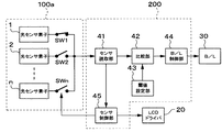
電気光学装置としての液晶装置は、パネル内光センサ部100を備えた透過型の液晶パネル10と、液晶パネル10を駆動するLCDドライバ20と、液晶パネル10の背面に設けられてバックライト光を照射するバックライト(B/Lと略記)30と、パネル内光センサ部100,LCDドライバ20及びバックライト30にそれぞれ制御信号を送って、光センサ部100の複数の光センサ素子を切り替える制御、未使用の光センサ素子を遮光する制御、及び、バックライト光の輝度を調整する制御を行う制御部200と、を備えている。
A liquid crystal device as an electro-optical device includes a transmissive
液晶パネル10は、後述するように(図1及び図2参照)、画素部12の一部である画素電極を有する素子基板11とこの素子基板11と対向して配置される対向電極15を有する対向基板14との間に電気光学物質としての液晶18が挟持され、素子基板11上には複数のデータ線(図示略)と複数の走査線(図示略)との交差に対応して設けられた複数の画素部12から成る表示領域としての画素領域を備えている。
As will be described later (see FIGS. 1 and 2), the
液晶パネル10は、画素領域10Aの複数の画素部12にそれぞれ画素スイッチング素子として図示しない薄膜トランジスタ(以下、TFT)を用いたアクティブマトリクス方式の液晶パネルであって、パネル内にはTFTと同様のプロセスで光センサ部100が形成されている。
光センサ部100は、素子基板11上の前記画素領域10Aが配置されている領域の端部に形成され(図1参照)、外光を受光してその照度を検出する。
The
The
光センサ部100は、複数の光センサ素子(例えば図4参照)と、これらの光センサ素子の中から少なくとも1つを、使用する光センサ素子として選択する複数のセンサ選択用スイッチSW1〜SWn(例えば図4参照)から成る選択手段とを備え、外光照度検出時には、少なくとも1つの光センサ素子で照度検出を行う。そして、制御部200は、その使用していた光センサ素子が劣化した場合、その劣化を検出し、前記選択手段を制御して別の光センサ素子に切り替える制御を行うことが可能である。
制御部200は、図3に示すようにセンサ読取部41と、比較部42と、閾値設定部43と、バックライト制御部(以下、B/L制御部)44と、センサ制御部45とを備えている。
The
As shown in FIG. 3, the
光センサ部100を構成する複数の光センサ素子(例えば図4参照)のうちの少なくとも1つの光センサ素子で検出した外光照度情報をセンサ読取部41にて電流/電圧変換する。その後、比較部42においてそのアナログ情報(電圧)をA/D変換し、閾値設定部43からの閾値と比較することによって、その比較結果情報をもとにB/L制御部44は所望の関数に従ってバックライト30の発光量を制御し、バックライト輝度を自動的に調整する。これにより、外光の明るさに応じてバックライト30の輝度を調整して画面を見易くしたり、或いは外光のない暗所においては画面の明るさを低下させる制御を行うことにより、消費電力を抑えたりすることができる。
The ambient light illuminance information detected by at least one of the plurality of optical sensor elements (for example, see FIG. 4) constituting the
一方、光センサ部100の光センサ素子の劣化の判断はセンサ制御部45が行う。センサ制御部45は使用している光センサ素子の例えば使用時間あるいは使用回数をカウントおり、センサ制御部45内に記憶された使用時間或いは使用回数の上限値情報と比較することによって劣化したかどうかを判断する。センサ使用時間或いは使用回数の上限値情報は外部から設定可能であり、書換え可能である。センサ制御部45は、劣化したことを判断すると、センサ部100内の前記選択手段を制御して、使用していた光センサ素子を別の光センサ素子に切り替える制御を行う。
On the other hand, the
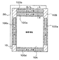
図1は本発明の第1の実施形態の電気光学装置における液晶パネル10及びその背面のバックライト30の配置と、液晶パネル10の表示領域(画素領域)10Aの周辺部に存在可能な非表示領域10Bにおける5つの光センサ部100a〜100eの配置領域を示している。この5つの配置領域は、例えば携帯電話機等のモバイル機器の表示領域の周辺部において、光センサ部の配設位置として可能と考えられる領域である。
FIG. 1 shows the arrangement of the
図2は図1における液晶パネルのA−A’線断面図を示している。素子基板11に対向して対向基板14が配置され、両基板間には液晶18が挟持されている。素子基板11の下面には下偏光板13が配設され、素子基板11に対向する対向基板14の下面には対向電極15が配設され対向基板14の上面には上偏光板16が配設されている。
FIG. 2 is a cross-sectional view taken along the line A-A ′ of the liquid crystal panel in FIG. 1. A
画素電極及び画素スイッチング素子(TFT)を含む画素部12はアクティブマトリクス基板である素子基板11上に形成されている。また、光センサ部100a,100bもアクティブマトリクス基板である素子基板11上に形成されている。従って、光センサ部100a,100bは、画素部12を形成するプロセスにて、同時に作成することができる。
さらに、本実施形態では、光センサ部100a,100bの上部にそれぞれ偏光部101a,101bを配置し、さらにその上に透明電極102a,102bを配置する。このとき偏光部101a,101bは下偏光板として機能する。このように構成することにより、光センサ部の上部に上偏光板16、液晶層18、下偏光板101a,101bのある構造となる。なお、偏光部101a,101bは百数十nm程度のピッチでアルミニウム等をパターニングすることで形成できる。
A
Further, in the present embodiment, the
図2は、外光を液晶パネル10内の光センサ部100aに対して照射させた場合に、液晶18の配向制御によって、光センサ部100aの複数の光センサ素子のうちで使用する光センサ素子へは外光を照射して外光照度の検出ができるようにし、光センサ部100bについては全ての光センサ素子への外光の照射を遮光することが可能であることを示している。すなわち、光センサ部100aの使用する光センサ素子の上部の液晶18の配向状態を制御して、光が偏光部101aを通過できるようにする一方、光センサ部100bの全ての光センサ素子の上部に存在可能な液晶18の配向状態を制御して、光が偏光部101bを通過しないように制御している。光センサ部100aの光センサ素子の上部の液晶18を配向制御するには、透明電極102aと対向電極15間に電圧を印加することによって行う。
FIG. 2 shows an optical sensor element used among a plurality of optical sensor elements of the
本実施形態では、光センサ素子を液晶パネル10内に複数個形成し、使用光センサ素子と未使用光センサ素子に分ける。使用していた光センサ素子が劣化した場合、外光照度検出を未使用光センサ素子に切り替えることによって、所望のダイナミックレンジで(換言すれば所望の感度で)外光照度検出を長期間にわたって実行できるようにする。使用する光センサ素子のみに光照射させ、未使用光センサ素子は遮光する制御を、光センサ素子の上部の液晶を利用して行うことによって、未使用光センサ素子に外光が照射されて光劣化するのを防止することができる。また、未使用光センサ素子は遮光されるとともに、選択手段によって電気的にもセンサ読取部とは切り離されるため、電流発生に基づく電気的な劣化も防止できる。
In the present embodiment, a plurality of photosensor elements are formed in the
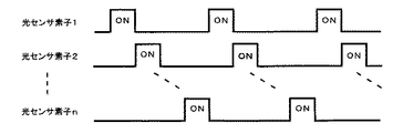
図4は第1の実施形態における、光センサ素子の劣化を判定して、自動的に複数の光センサ素子を切り替えて、外光照度検出を長期間に亘って維持させる電気回路の構成例のブロック図を示している。図5は図4の回路における光センサ素子の切り替えタイミングを示すタイミングチャートである。 FIG. 4 is a block diagram of a configuration example of an electric circuit that determines deterioration of an optical sensor element, automatically switches a plurality of optical sensor elements, and maintains external light illuminance detection for a long period in the first embodiment. The figure is shown. FIG. 5 is a timing chart showing the switching timing of the optical sensor elements in the circuit of FIG.
図4において、光センサ部100aは、複数の光センサ素子1〜n(nは2以上の整数)と、これらの光センサ素子1〜nの中から使用する光センサ素子として少なくとも1つの光センサ素子を選択するセンサ選択用スイッチSW1〜SWnで構成される選択手段とを備え、外光検出時には、選択された少なくとも1つの光センサ素子(例えば光センサ素子1)で照度検出を行う。そして、その使用していた光センサ素子が劣化した場合、前記選択手段を制御して別の光センサ素子(例えば光センサ素子2〜nのいずか)に切り替えて使用するようになっている。
In FIG. 4, the
次に、外光の検出方法を以下に説明する。
まず、光センサ素子1を劣化するまで使用し続ける。このとき、センサ制御部45はスイッチSW1のみをオンさせている。同時に光センサ部100aにおける光センサ素子1の上部の液晶18を駆動させるための信号を、LCDドライバ20ヘ信号を送る。これによって光センサ素子1に外光が照射されるようになっている。センサ制御部45は、光センサ素子1が劣化したと判断した場合、スイッチSW1をオフ、スイッチSW2をオンし、次の光センサ素子2を使用する。このとき、光センサ素子1の上部の液晶18を遮光状態にする信号をLCDドライバ20へ送ると同時に、光センサ部100aにおける光センサ素子2の上部の液晶18を駆動させるための信号を、LCDドライバ20ヘ信号を送る。これによって光センサ素子2に外光が照射されるようになる。以下同様に劣化するまで光センサ素子2を使用しつづけ、劣化したと判断したら光センサ素子のスイッチを切り替え、次の光センサ素子を使用する。
Next, a method for detecting outside light will be described below.
First, the
光センサ素子の劣化の判断はセンサ制御部45が行う。センサ制御部45は、使用しているセンサの使用時間あるいは使用回数をカウントおり、センサ制御部45内に記憶された使用時間あるいは使用回数の上限値情報と比較することで劣化したかどうかを判断する。
The
センサ制御部45は、一度使用した光センサ素子は劣化しているため、再使用はしない制御を行う。また、センサ制御部45に設定されるセンサ使用時間あるいは使用回数の上限値情報は外部から設定可能であり、書換え可能である。
The
第1の実施形態によれば、複数の光センサ素子を用意して、1つの光センサ素子が使用不能となる前に、1つの光センサ素子が劣化したことを判断して、次の光センサ素子に切り替えていき、全ての光センサ素子を使用することになるので、長期間に亘って外光をセンシングして電気光学装置のバックライト調光制御等に用いることが可能となる。 According to the first embodiment, a plurality of photosensor elements are prepared, and it is determined that one photosensor element has deteriorated before one photosensor element becomes unusable. Since all the optical sensor elements are used by switching to the element, it is possible to sense outside light over a long period of time and use it for backlight dimming control of the electro-optical device.
[第2の実施形態]
第2の実施形態の電気光学装置における液晶パネル10及びその背面のバックライト30の配置と、液晶パネル10の表示領域(画素領域)10Aの周辺部に存在可能な非表示領域10Bにおける5つの光センサ部100a〜100eの配置領域、及び、液晶パネル10の断面構造は、第1の実施形態の図1及び図2と同様であるので、説明を省略する。
[Second Embodiment]
The arrangement of the
また、第2の実施形態における、光センサ素子の劣化を判定して、自動的に光センサ素子を切り替えて、外光照度検出を長期間に亘って維持させる電気回路の構成例のブロック図については、図4と同様であり、図示を省略してある。 Also, in the second embodiment, a block diagram of a configuration example of an electric circuit that determines deterioration of an optical sensor element, automatically switches the optical sensor element, and maintains external light illuminance detection for a long period of time. 4 is the same as FIG. 4 and is not shown.
図6は本発明の第2実施形態の電気光学装置における光センサ素子の切り替えタイミングを示すタイミングチャートである。図4のブロック図を参照しながら説明する。 FIG. 6 is a timing chart showing the switching timing of the optical sensor element in the electro-optical device according to the second embodiment of the invention. This will be described with reference to the block diagram of FIG.
まず、光センサ素子が劣化する前の一定期間(例えば数時間、図示のONの期間)だけ光センサ素子1を使用する。光センサ素子1の使用回数がある回数に達したら、スイッチSW1をオフ、スイッチSW2をオンし光センサ素子2を使用する。以下同様に、光センサ素子nまで使用していき、再度光センサ素子1から使用するというように光センサ素子を切り換えていく。
First, the
センサ制御部45には、光センサ素子の1回当たりの一定の使用期間と、繰り返しの一定の使用回数とが予め記憶されており、光センサ素子の一定の使用期間の情報に従って光センサ素子を順次切り替えていき、各々の光センサ素子を規定の繰り返し使用回数だけ使用する。
The
第2の実施形態によれば、複数の光センサ素子を用意して、その複数の光センサ素子を各々一定期間ずつサイクリックに繰り返し使用し、各々の繰り返し使用回数が一定回数に達したときに劣化したものとする。複数の光センサ素子がほぼ同時に劣化していくことになる。これによって、長期間に亘って外光をセンシングして電気光学装置のバックライト調光制御等に用いることが可能となる。 According to the second embodiment, when a plurality of photosensor elements are prepared, and each of the plurality of photosensor elements is cyclically used repeatedly for a certain period, and each of the repeated use times reaches a certain number of times. Assume that it has deteriorated. A plurality of optical sensor elements will deteriorate almost simultaneously. Accordingly, it is possible to sense outside light for a long period of time and use it for backlight dimming control of the electro-optical device.
[第3の実施形態]
第3の実施形態の電気光学装置における液晶パネル10及びその背面のバックライト30の配置と、液晶パネル10の表示領域(画素領域)10Aの周辺部に存在可能な非表示領域10Bにおける5つの光センサ部100a〜100eの配置領域、及び、液晶パネル10の断面構造は、第1の実施形態の図1及び図2と同様であり、説明を省略する。
[Third Embodiment]
The arrangement of the
図7は、第3の実施形態における、光センサ素子の劣化を判定して、自動的に複数の光センサ素子を切り替えて、外光照度検出を長期間に亘って維持させる電気回路の構成例のブロック図を示している。
図8は図7における光センサ素子の切り替えタイミングを示すタイミングチャートである。このタイミングチャートは図5と類似したタイミングチャートとなっている。図7のブロック図を参照しながら説明する。
FIG. 7 shows an example of the configuration of an electric circuit that determines deterioration of an optical sensor element and automatically switches a plurality of optical sensor elements to maintain external light illuminance detection for a long period in the third embodiment. A block diagram is shown.
FIG. 8 is a timing chart showing the switching timing of the optical sensor elements in FIG. This timing chart is a timing chart similar to FIG. This will be described with reference to the block diagram of FIG.
図7において、図4の構成と異なる点は、光センサ部100a-1は外光照度検出用の複数の光センサ素子1〜n(nは2以上の整数)の他に、基準となる基準光センサ素子21を備えていることである。基準光センサ素子21は、基準センサ選択用スイッチSWrefを介して基準センサ読み取り部22に接続している。
In FIG. 7, the difference from the configuration of FIG. 4 is that the
一定期間光センサ素子1を使用した後、所定のタイミングにおいて基準光センサ素子21と光センサ素子1を同時にオンする。或いは、光センサ素子1を一定期間使用し、その使用を継続しているときに基準光センサ素子21を所定の期間ごとにオンすることによって、基準光センサ素子21と光センサ素子1を同時にオンしてもよい。
After using the
光センサ素子1と基準光センサ素子21それぞれのセンサ読取部41,21において、光センサ素子1と基準光センサ素子21の各々の光検出値を読み取り、センサ制御部45において検出値の比較(差分値検出)を行う。比較の結果、一定値以上の差が生じた場合、光センサ素子1は劣化したと判断し、光センサ素子2を使用する。以下同様に光センサ素子nまで繰り返す。センサ制御部45には、基準光センサ素子21をオンするタイミングの情報が記憶され、かつ光センサ素子の劣化を判断するため光センサ素子と基準光センサ素子との光検出値の差の上限値も記憶されている。
The
ここで、基準光センサ素子21のオン期間は短期間(例えば0.5〜1秒程度)であり、光センサ素子1〜nそれぞれのオン期間は長い期間(例えば数百時間)である。従って、例えば光センサ素子1〜nの各光センサ素子について少なくとも数十時間オンした後の期間に、基準光センサ素子21の最初のオンがされて、光検出値同士の比較を行うように制御してもよい。なお、基準光センサ素子21のオン期間は上記のように非常の短いので、そのオン時の受光動作によって基準光センサ素子21が劣化することは殆どなく、従って1つ基準光センサ素子を用いてn個の光センサ素子を長期間に亘って劣化判定の基準として使用することができる。
Here, the on period of the
第3の実施形態によれば、外光照度検出用の複数の光センサ素子のほかに、使用中の光センサ素子の劣化判断を行うための基準となる基準光センサ素子を設けて、使用中の光センサ素子の光検出値と基準光センサ素子の光検出値との差を得、一定値以上の差が生じた場合、1つの光センサ素子が劣化したことを判断して、次の光センサ素子に切り替えていき、全ての光センサ素子を使用することになるので、長期間に亘って外光をセンシングして電気光学装置のバックライト調光制御等に用いることが可能となる。 According to the third embodiment, in addition to the plurality of light sensor elements for detecting the illuminance of external light, the reference light sensor element serving as a reference for performing the deterioration determination of the light sensor element in use is provided, When the difference between the photodetection value of the photosensor element and the photodetection value of the reference photosensor element is obtained and a difference of a certain value or more occurs, it is determined that one photosensor element has deteriorated, and the next photosensor Since all the optical sensor elements are used by switching to the element, it is possible to sense outside light over a long period of time and use it for backlight dimming control of the electro-optical device.
[第4の実施形態]
第4の実施形態の電気光学装置における液晶パネル10及びその背面のバックライト30の配置と、液晶パネル10の表示領域(画素領域)10Aの周辺部に存在可能な非表示領域10Bにおける5つの光センサ部100a〜100eの配置領域、及び、液晶パネル10の断面構造は、第1の実施形態の図1及び図2と同様であるので、説明を省略する。
[Fourth Embodiment]
The arrangement of the
図9は、第4の実施形態における、光センサ素子の劣化を判定して、自動的に複数の光センサ素子を切り替えて、外光照度検出を長期間に亘って維持させる電気回路の構成例のブロック図を示している。
図10は図9における光センサ素子の切り替えタイミングを示すタイミングチャートである。このタイミングチャートでは、複数の光センサ素子がほぼ同時に劣化していき、その点で図6と類似したタイミングチャートとなっている。図9のブロック図を参照しながら説明する。
FIG. 9 shows an example of the configuration of an electric circuit that determines deterioration of an optical sensor element, automatically switches a plurality of optical sensor elements, and maintains external light illuminance detection for a long period in the fourth embodiment. A block diagram is shown.
FIG. 10 is a timing chart showing the switching timing of the optical sensor elements in FIG. In this timing chart, the plurality of optical sensor elements deteriorate almost simultaneously, and the timing chart is similar to that in FIG. This will be described with reference to the block diagram of FIG.
図9において、図4の構成と異なる点は、光センサ部100a-2は外光照度検出用の複数の光センサ素子1〜n(nは2以上の整数)の他に、基準となる基準光センサ素子21を備えていることである。従って基準光センサ素子21を有する点では、図7の構成と類似した構成となっている。スイッチSW1’〜SWn’はいずれも、光センサ素子からの外光照度検出出力を入力する入力端eと、光センサ素子からの外光照度検出出力をセンサ読み取り部41に導く出力端fと、光センサ素子からの遮光時のリーク検出出力を基準センサ読み取り部22に導く出力端gと、を有している。基準光センサ素子21は、スイッチSWrefを介して基準センサ読み取り部22に接続している。基準光センサ素子21は遮光状態でのリーク電流を検出し、基準センサ読み取り部21はこのリーク電流の検出に続いて(又は同時に)、センサ切替用スイッチ(例えばSW1’)を用いて、使用した光センサ素子(例えば光センサ素子1)の遮光時のリーク電流を検出し、リーク電流同士を比較し、両者の差分値が一定以上の大きさであれば、劣化したと判断する構成となっている。
9, the
基準光センサ素子21は常時遮光状態で使用する。従って、本実施形態での基準光センサ素子は光照射によって劣化することがない。光センサ素子1を一定期間(例えば、数時間)外光照度検出に使用した後、光センサ素子2に切り換えるといった順で光センサ素子を切り替えて使用する。光センサ素子nを使用した後は、再度光センサ素子1に切り替えて使用する。光センサ素子1は一定期間外光照度検出に使用した後、センサ切替用スイッチSW1’を切り替えて基準センサ読み取り部22と接続する。基準センサ読み取り部22では使用した光センサ素子1の遮光時のリーク電流を検出する。センサ制御部45で光センサ素子1の遮光時の検出値と基準光センサ素子21の検出値の比較を行う。センサ制御部45は、光センサ素子1の検出値が基準光センサ素子21の検出値と一定以上の差が生じた場合、光センサ素子は劣化したと判断し、以降劣化した光センサ素子ヘの切り替えは行わず(即ち、その劣化した光センサ素子を飛ばして)別の光センサ素子へ切り替える制御を行う。
The reference
また、本実施形態では、複数の光センサ素子を各々一定期間ずつサイクリックに繰り返し使用する。光センサ素子の劣化を検出するのは、光センサ素子を一定期間使用した後の未使用期間(休止期間)に遮光した状態で行う必要があるため、光センサ素子の劣化判断時には、光センサ素子1〜nのいずれか及び基準光センサ素子21のそれぞれの上部の液晶の駆動を停止させて遮光状態とするように液晶制御を行っておくことが必要である。
In this embodiment, a plurality of photosensor elements are repeatedly used cyclically for a certain period. Since it is necessary to detect the deterioration of the optical sensor element in a non-use period (resting period) after the optical sensor element has been used for a certain period of time, the optical sensor element is used when determining the deterioration of the optical sensor element. It is necessary to perform liquid crystal control so that driving of the liquid crystal on any one of 1 to n and the reference
第4の実施形態によれば、外光照度検出用の複数の光センサ素子のほかに、使用中の光センサ素子の劣化判断を行うための基準となる基準光センサ素子を設けて、複数の光センサ素子を各々一定期間ずつサイクリックに使用する過程で、遮光時の光センサ素子のリーク電流検出値と、遮光状態での基準光センサ素子のリーク電流検出値との差をとることによって、一定値以上の差が生じた場合、1つの光センサ素子が劣化したことを判断して、次の光センサ素子に切り替えていくので、長期間に亘って外光をセンシングして電気光学装置のバックライト調光制御等に用いることが可能となる。 According to the fourth embodiment, in addition to a plurality of light sensor elements for detecting the illuminance of outside light, a reference light sensor element serving as a reference for determining deterioration of a light sensor element in use is provided, and a plurality of light sensors are provided. In the process of cyclically using each sensor element for a certain period, a constant is obtained by taking the difference between the leak current detection value of the photosensor element during light shielding and the leak current detection value of the reference photosensor element in the light shielding state. When a difference greater than the value occurs, it is judged that one photosensor element has deteriorated and the next photosensor element is switched. It can be used for light dimming control and the like.
上述した実施形態に係る電気光学装置は、携帯電話機等の電子機器に適用される。
次に、上述した実施形態に係る電気光学装置を表示装置として有する電子機器について説明する。
The electro-optical device according to the above-described embodiment is applied to an electronic device such as a mobile phone.
Next, an electronic apparatus having the electro-optical device according to the above-described embodiment as a display device will be described.
図11は電子機器として携帯電話の外観を示す斜視図である。
図11に示すように、携帯電話機200は、複数の操作ボタン201の他に、受話口202、送話口203と共に、上述した電気光学装置としての表示装置を構成する表示部205を有する。表示部205の画素領域が配置されている領域の端部には、複数の光センサ素子を有する光センサ部(図示せず)が形成されている。これにより、外光をセンシングして電気光学装置のバックライト調光制御等に長期間に亘って用いることが可能となる。
FIG. 11 is a perspective view illustrating an appearance of a mobile phone as an electronic device.
As shown in FIG. 11, the
本発明の電気光学装置は、液晶装置だけではなく、電気光学物質にR,G,B等の映像信号を供給して表示を行うエレクトロルミネッセンス装置、有機エレクトロルミネッセンス装置、プラズマディスブレイ装置、電気泳動ディスプレイ装置、電子放出素子を用いた装置(Field Emission Display 及び Surface-Conduction Electron-Emitter Display等)などの各種の電気光学装置においても本発明を同様に適用することが可能である。 The electro-optical device of the present invention is not limited to a liquid crystal device, but an electroluminescent device, an organic electroluminescent device, a plasma display device, an electrophoretic device that displays images by supplying image signals such as R, G, and B to an electro-optical material. The present invention can be similarly applied to various electro-optical devices such as a display device and a device using an electron-emitting device (Field Emission Display, Surface-Conduction Electron-Emitter Display, etc.).
なお、本発明は、半導体基板に素子を形成する表示用デバイス、例えばLCOS(Liquid Crysta1 On Silicon)などにも適用可能である。
LCOSでは素子基板として単結晶シリコン基板を用い、画素や周辺回路に用いるスイッチング素子としてトランジスタを単結晶シリコン基板に形成する。また、画素には反射型の画素電極を用い、画素電極の下層に画素の各素子を形成する。
The present invention can also be applied to a display device for forming an element on a semiconductor substrate, for example, LCOS (
In LCOS, a single crystal silicon substrate is used as an element substrate, and a transistor is formed on a single crystal silicon substrate as a switching element used for a pixel or a peripheral circuit. In addition, a reflective pixel electrode is used for the pixel, and each element of the pixel is formed under the pixel electrode.
なお、本発明の電気光学装置が適用される電子機器としては、携帯電話機の他にも、テレビジョンや、ビューファインダ型・モニタ直視型のビデオテープレコーダ、カーナビゲーション装置、ページャ、電子手帳、電卓、ワードプロセッサ、ワークステーション、テレビ電話、POS端末、ディジタルスチルカメラ、タッチパネルを備えた機器等などが挙げられる。 Electronic devices to which the electro-optical device of the present invention is applied include, in addition to mobile phones, televisions, viewfinder type / monitor direct view type video tape recorders, car navigation devices, pagers, electronic notebooks, calculators. , Word processors, workstations, videophones, POS terminals, digital still cameras, devices equipped with touch panels, and the like.
1〜n…光センサ素子、10…液晶パネル、10A…画素領域(表示領域)、11…素子基板、12…画素部、14…対向基板、15…対向電極、18…液晶(電気光学物質)、21…基準光センサ素子、22…基準センサ読み取り部、41…基準センサ読み取り部、45…センサ制御部、100,100a,100b…光センサ部、101a,101b…偏光部、102a,102b…透明電極、200…制御部、SW1〜SWn…センサ選択用スイッチ、SWref…基準センサ選択用スイッチ。 DESCRIPTION OF SYMBOLS 1-n ... Optical sensor element, 10 ... Liquid crystal panel, 10A ... Pixel area | region (display area), 11 ... Element board | substrate, 12 ... Pixel part, 14 ... Opposite substrate, 15 ... Counter electrode, 18 ... Liquid crystal (electro-optical substance) , 21 ... reference light sensor element, 22 ... reference sensor reading unit, 41 ... reference sensor reading unit, 45 ... sensor control unit, 100, 100a, 100b ... light sensor unit, 101a, 101b ... polarizing unit, 102a, 102b ... transparent Electrode, 200... Control unit, SW1 to SWn, sensor selection switch, SWref, reference sensor selection switch.
Claims (7)
前記対向基板上に偏光板が配置され、
前記素子基板上に形成され、外光の照度を検出する光センサ部と、
該光センサ部の上に形成された偏光部と、
該偏光部の上に形成された透明電極と、
前記光センサ部における複数の光センサ素子とこれらの光センサ素子の中から少なくとも1つを使用する光センサ素子として選択する選択手段と、
を具備し、
前記光センサ部の上部の前記透明電極を電気的に制御することによって、該光センサ部を遮光可能としたことを特徴とする電気光学装置。 An electro-optical material is sandwiched between an element substrate having a pixel electrode corresponding to the intersection of a plurality of scanning lines and a plurality of data lines, and a counter substrate having a counter electrode disposed to face the element substrate. In the electro-optical device in which the display area is formed,
A polarizing plate is disposed on the counter substrate,
An optical sensor unit formed on the element substrate for detecting the illuminance of external light;
A polarizing part formed on the photosensor part;
A transparent electrode formed on the polarizing part;
A plurality of photosensor elements in the photosensor unit, and a selection means for selecting at least one of these photosensor elements as an optical sensor element;
Comprising
An electro-optical device characterized in that the optical sensor unit can be shielded by electrically controlling the transparent electrode on the optical sensor unit.
前記制御部は、前記複数の光センサ素子のうちの第1の光センサ素子を前記選択手段にて選択するとともに、該第1の光センサ素子における上部の透明電極を電気的に制御して、第1の光センサ素子への外光照射を可能とし、前記第1の光センサ素子を一定期間ごとに前記基準光センサ素子と同時に光検出値を行うことで当該光検出の差分値に応じて劣化を判断し、前記選択手段にて、前記複数の光センサ素子の最後の光センサ素子まで外光照度検出を継続して実行させることを特徴とする請求項2に記載の電気光学装置。 The plurality of photosensor elements includes a reference photosensor element that serves as a deterioration determination standard other than a predetermined number of external light illuminance detection photosensor elements,
The control unit selects a first photosensor element of the plurality of photosensor elements by the selection means, and electrically controls an upper transparent electrode in the first photosensor element, According to the difference value of the light detection by enabling external light irradiation to the first photosensor element and performing the photodetection value simultaneously with the reference photosensor element for the first photosensor element at regular intervals 3. The electro-optical device according to claim 2, wherein deterioration is determined, and the selection unit continuously executes ambient light illuminance detection until the last photosensor element of the plurality of photosensor elements.
前記制御部は、前記複数の光センサ素子のうちの第1の光センサ素子を前記選択手段にて、使用する光センサ素子として選択するとともに、該第1の光センサ素子における上部の透明電極を電気的に制御して、第1の光センサ素子への外光照射を可能とし、その第1の光センサ素子から最後のセンサ素子までを予め決めた一定の使用時間だけ使用して切り替え、前記第1の光センサ素子の遮光時のリーク電流の検出値と前記基準光センサ素子のリーク電流の検出値との差分に応じて前記第1の光センサ素子が劣化したと判断し、以降劣化した光センサ素子への切り替えを行わず未劣化の光センサ素子に切り替えて同様な劣化検出を行い、前記複数の光センサ素子の最後の光センサ素子まで外光照度検出を継続して実行させることを特徴とする請求項2に記載の電気光学装置。 In addition to a predetermined number of external light illuminance detection optical sensor elements, the plurality of optical sensor elements include a reference optical sensor element that serves as a reference for deterioration determination, and the reference optical sensor element is used in a light-shielded state.
The control unit selects a first photosensor element of the plurality of photosensor elements as a photosensor element to be used by the selection unit, and selects an upper transparent electrode in the first photosensor element. Electrically controlled to allow external light irradiation to the first photosensor element, switching from the first photosensor element to the last sensor element using a predetermined fixed use time, It is determined that the first photosensor element has deteriorated according to the difference between the leak current detection value when the first photosensor element is shielded and the leak current detection value of the reference photosensor element. The same deterioration detection is performed by switching to an undegraded photosensor element without switching to the photosensor element, and the ambient light illuminance detection is continuously performed until the last photosensor element of the plurality of photosensor elements. Claim 2. The electro-optical device according to 2.
Priority Applications (1)
| Application Number | Priority Date | Filing Date | Title |
|---|---|---|---|
| JP2006243743A JP4765852B2 (en) | 2006-09-08 | 2006-09-08 | Electro-optical device and electronic apparatus |
Applications Claiming Priority (1)
| Application Number | Priority Date | Filing Date | Title |
|---|---|---|---|
| JP2006243743A JP4765852B2 (en) | 2006-09-08 | 2006-09-08 | Electro-optical device and electronic apparatus |
Publications (3)
| Publication Number | Publication Date |
|---|---|
| JP2008065107A JP2008065107A (en) | 2008-03-21 |
| JP2008065107A5 JP2008065107A5 (en) | 2009-03-12 |
| JP4765852B2 true JP4765852B2 (en) | 2011-09-07 |
Family
ID=39287872
Family Applications (1)
| Application Number | Title | Priority Date | Filing Date |
|---|---|---|---|
| JP2006243743A Active JP4765852B2 (en) | 2006-09-08 | 2006-09-08 | Electro-optical device and electronic apparatus |
Country Status (1)
| Country | Link |
|---|---|
| JP (1) | JP4765852B2 (en) |
Families Citing this family (5)
| Publication number | Priority date | Publication date | Assignee | Title |
|---|---|---|---|---|
| KR101343105B1 (en) * | 2007-12-18 | 2013-12-20 | 삼성디스플레이 주식회사 | Light sensor inspection unit, method of inspecting the same and display device |
| JP5057340B2 (en) * | 2008-03-31 | 2012-10-24 | 株式会社ジャパンディスプレイウェスト | Photodetection device, electro-optical device, and electronic apparatus |
| TWI403789B (en) * | 2009-04-01 | 2013-08-01 | Acer Inc | Liquid crystal display panel, liquid crystal display device, light detection device and light intensity adjustment method |
| DE102013105229A1 (en) * | 2013-05-22 | 2014-11-27 | Osram Opto Semiconductors Gmbh | Optoelectronic component and method for producing an optoelectronic component |
| JP2015025834A (en) * | 2013-07-24 | 2015-02-05 | セイコーエプソン株式会社 | Electro-optic device and electronic instrument |
Family Cites Families (1)
| Publication number | Priority date | Publication date | Assignee | Title |
|---|---|---|---|---|
| JP4048627B2 (en) * | 1998-10-20 | 2008-02-20 | カシオ計算機株式会社 | Display device |
-
2006
- 2006-09-08 JP JP2006243743A patent/JP4765852B2/en active Active
Also Published As
| Publication number | Publication date |
|---|---|
| JP2008065107A (en) | 2008-03-21 |
Similar Documents
| Publication | Publication Date | Title |
|---|---|---|
| US7443463B2 (en) | Liquid crystal display device and luminance difference compensating method thereof | |
| CN107221281B (en) | Display panel and display device | |
| JP4007390B2 (en) | Electro-optical device and electronic apparatus | |
| JP4353224B2 (en) | Photodetection device, electro-optical device, and electronic apparatus | |
| JP4557228B2 (en) | Electro-optical device and electronic apparatus | |
| US7995026B2 (en) | Sensor and display device including the sensor | |
| JP2007065004A (en) | Illuminance detecting method, luminance control method, electro-optical device, and electronic equipment | |
| US7223958B2 (en) | Device for and method of driving an electro-optical device | |
| US20100141598A1 (en) | Display, display driving method, and electronic apparatus | |
| JP4765852B2 (en) | Electro-optical device and electronic apparatus | |
| JP2007248816A (en) | Electro-optical device and electronic equipment | |
| JPWO2010125840A1 (en) | Display device | |
| JP4797521B2 (en) | Electro-optical device, illuminance detection method of electro-optical device, and electronic apparatus | |
| JPH04254820A (en) | Liquid crystal display | |
| JP4656082B2 (en) | Electro-optical device and electronic apparatus | |
| JP2008064828A (en) | Liquid crystal device and electronic apparatus | |
| JP2008070616A (en) | Electro-optical device and method of determining its optical sensor failure | |
| JP2007316196A (en) | Display device | |
| JP2007248956A (en) | Electro-optical device and electronic equipment | |
| US8487860B2 (en) | Circuit and method for driving, electro-optic device, and electronic apparatus | |
| JP2007018846A (en) | Lighting device, electro-optical device with lighting device, and electronic apparatus | |
| KR20070042803A (en) | Gamma reference voltage circuit and liquid crystal display having the same | |
| JP2010145811A (en) | Liquid crystal device, electro-optical device, and driving method of liquid crystal device | |
| JP5312435B2 (en) | Display device | |
| JP2007018845A (en) | Lighting device, electro-optical device equipped with lighting device, adjusting method of optical property using electro-optical device, and electronic apparatus |
Legal Events
| Date | Code | Title | Description |
|---|---|---|---|
| A521 | Request for written amendment filed |
Free format text: JAPANESE INTERMEDIATE CODE: A523 Effective date: 20090126 |
|
| A621 | Written request for application examination |
Free format text: JAPANESE INTERMEDIATE CODE: A621 Effective date: 20090126 |
|
| A711 | Notification of change in applicant |
Free format text: JAPANESE INTERMEDIATE CODE: A711 Effective date: 20100526 |
|
| RD02 | Notification of acceptance of power of attorney |
Free format text: JAPANESE INTERMEDIATE CODE: A7422 Effective date: 20100526 |
|
| A977 | Report on retrieval |
Free format text: JAPANESE INTERMEDIATE CODE: A971007 Effective date: 20101126 |
|
| TRDD | Decision of grant or rejection written | ||
| A01 | Written decision to grant a patent or to grant a registration (utility model) |
Free format text: JAPANESE INTERMEDIATE CODE: A01 Effective date: 20110517 |
|
| A61 | First payment of annual fees (during grant procedure) |
Free format text: JAPANESE INTERMEDIATE CODE: A61 Effective date: 20110530 |
|
| R151 | Written notification of patent or utility model registration |
Ref document number: 4765852 Country of ref document: JP Free format text: JAPANESE INTERMEDIATE CODE: R151 |
|
| FPAY | Renewal fee payment (event date is renewal date of database) |
Free format text: PAYMENT UNTIL: 20140624 Year of fee payment: 3 |
|
| FPAY | Renewal fee payment (event date is renewal date of database) |
Free format text: PAYMENT UNTIL: 20140624 Year of fee payment: 3 |
|
| S111 | Request for change of ownership or part of ownership |
Free format text: JAPANESE INTERMEDIATE CODE: R313113 |
|
| FPAY | Renewal fee payment (event date is renewal date of database) |
Free format text: PAYMENT UNTIL: 20140624 Year of fee payment: 3 |
|
| R350 | Written notification of registration of transfer |
Free format text: JAPANESE INTERMEDIATE CODE: R350 |
|
| R250 | Receipt of annual fees |
Free format text: JAPANESE INTERMEDIATE CODE: R250 |
|
| R250 | Receipt of annual fees |
Free format text: JAPANESE INTERMEDIATE CODE: R250 |
|
| R250 | Receipt of annual fees |
Free format text: JAPANESE INTERMEDIATE CODE: R250 |
|
| R250 | Receipt of annual fees |
Free format text: JAPANESE INTERMEDIATE CODE: R250 |
|
| R250 | Receipt of annual fees |
Free format text: JAPANESE INTERMEDIATE CODE: R250 |
|
| R250 | Receipt of annual fees |
Free format text: JAPANESE INTERMEDIATE CODE: R250 |
|
| R250 | Receipt of annual fees |
Free format text: JAPANESE INTERMEDIATE CODE: R250 |
|
| S111 | Request for change of ownership or part of ownership |
Free format text: JAPANESE INTERMEDIATE CODE: R313111 |
|
| R250 | Receipt of annual fees |
Free format text: JAPANESE INTERMEDIATE CODE: R250 |
|
| R350 | Written notification of registration of transfer |
Free format text: JAPANESE INTERMEDIATE CODE: R350 |
|
| R250 | Receipt of annual fees |
Free format text: JAPANESE INTERMEDIATE CODE: R250 |
|
| R250 | Receipt of annual fees |
Free format text: JAPANESE INTERMEDIATE CODE: R250 |