JP4741792B2 - Manufacturing method of nitride semiconductor MIS type field effect transistor - Google Patents
Manufacturing method of nitride semiconductor MIS type field effect transistor Download PDFInfo
- Publication number
- JP4741792B2 JP4741792B2 JP2003421001A JP2003421001A JP4741792B2 JP 4741792 B2 JP4741792 B2 JP 4741792B2 JP 2003421001 A JP2003421001 A JP 2003421001A JP 2003421001 A JP2003421001 A JP 2003421001A JP 4741792 B2 JP4741792 B2 JP 4741792B2
- Authority
- JP
- Japan
- Prior art keywords
- nitride semiconductor
- insulating film
- field effect
- effect transistor
- containing nitrogen
- Prior art date
- Legal status (The legal status is an assumption and is not a legal conclusion. Google has not performed a legal analysis and makes no representation as to the accuracy of the status listed.)
- Expired - Lifetime
Links
- 239000004065 semiconductor Substances 0.000 title claims description 101
- 150000004767 nitrides Chemical class 0.000 title claims description 98
- 230000005669 field effect Effects 0.000 title claims description 39
- 238000004519 manufacturing process Methods 0.000 title claims description 25
- IJGRMHOSHXDMSA-UHFFFAOYSA-N Atomic nitrogen Chemical compound N#N IJGRMHOSHXDMSA-UHFFFAOYSA-N 0.000 claims description 146
- 229910052757 nitrogen Inorganic materials 0.000 claims description 73
- 229910052782 aluminium Inorganic materials 0.000 claims description 33
- 125000004430 oxygen atom Chemical group O* 0.000 claims description 28
- XAGFODPZIPBFFR-UHFFFAOYSA-N aluminium Chemical compound [Al] XAGFODPZIPBFFR-UHFFFAOYSA-N 0.000 claims description 27
- 125000004433 nitrogen atom Chemical group N* 0.000 claims description 16
- 238000000034 method Methods 0.000 claims description 13
- 238000004544 sputter deposition Methods 0.000 claims description 12
- 239000002356 single layer Substances 0.000 claims description 6
- 230000015572 biosynthetic process Effects 0.000 claims description 3
- 238000004140 cleaning Methods 0.000 claims description 2
- 238000001947 vapour-phase growth Methods 0.000 claims description 2
- TWNQGVIAIRXVLR-UHFFFAOYSA-N oxo(oxoalumanyloxy)alumane Chemical compound O=[Al]O[Al]=O TWNQGVIAIRXVLR-UHFFFAOYSA-N 0.000 description 46
- 239000010410 layer Substances 0.000 description 30
- PIGFYZPCRLYGLF-UHFFFAOYSA-N Aluminum nitride Chemical compound [Al]#N PIGFYZPCRLYGLF-UHFFFAOYSA-N 0.000 description 23
- PMHQVHHXPFUNSP-UHFFFAOYSA-M copper(1+);methylsulfanylmethane;bromide Chemical compound Br[Cu].CSC PMHQVHHXPFUNSP-UHFFFAOYSA-M 0.000 description 22
- 239000000758 substrate Substances 0.000 description 19
- 239000013078 crystal Substances 0.000 description 17
- 230000001681 protective effect Effects 0.000 description 13
- 229910002704 AlGaN Inorganic materials 0.000 description 12
- NBIIXXVUZAFLBC-UHFFFAOYSA-N Phosphoric acid Chemical compound OP(O)(O)=O NBIIXXVUZAFLBC-UHFFFAOYSA-N 0.000 description 10
- 229910018072 Al 2 O 3 Inorganic materials 0.000 description 9
- XKRFYHLGVUSROY-UHFFFAOYSA-N Argon Chemical compound [Ar] XKRFYHLGVUSROY-UHFFFAOYSA-N 0.000 description 8
- 229910004298 SiO 2 Inorganic materials 0.000 description 7
- 230000000694 effects Effects 0.000 description 7
- 239000012298 atmosphere Substances 0.000 description 6
- 238000003795 desorption Methods 0.000 description 6
- 238000005530 etching Methods 0.000 description 6
- 229910052737 gold Inorganic materials 0.000 description 6
- 229910052759 nickel Inorganic materials 0.000 description 6
- 239000012299 nitrogen atmosphere Substances 0.000 description 6
- 229910000147 aluminium phosphate Inorganic materials 0.000 description 5
- QJGQUHMNIGDVPM-UHFFFAOYSA-N nitrogen group Chemical group [N] QJGQUHMNIGDVPM-UHFFFAOYSA-N 0.000 description 5
- 229910052786 argon Inorganic materials 0.000 description 4
- QVGXLLKOCUKJST-UHFFFAOYSA-N atomic oxygen Chemical compound [O] QVGXLLKOCUKJST-UHFFFAOYSA-N 0.000 description 4
- 238000000605 extraction Methods 0.000 description 4
- 239000007789 gas Substances 0.000 description 4
- 238000010438 heat treatment Methods 0.000 description 4
- 239000001301 oxygen Substances 0.000 description 4
- 229910052760 oxygen Inorganic materials 0.000 description 4
- 230000007547 defect Effects 0.000 description 3
- 230000006866 deterioration Effects 0.000 description 3
- 238000010586 diagram Methods 0.000 description 3
- 230000015556 catabolic process Effects 0.000 description 2
- 238000011109 contamination Methods 0.000 description 2
- 230000001590 oxidative effect Effects 0.000 description 2
- -1 Al 2 O 3 Chemical class 0.000 description 1
- 229910004541 SiN Inorganic materials 0.000 description 1
- 238000009413 insulation Methods 0.000 description 1
- 230000007774 longterm Effects 0.000 description 1
- 229910052751 metal Inorganic materials 0.000 description 1
- 239000002184 metal Substances 0.000 description 1
- 229910044991 metal oxide Inorganic materials 0.000 description 1
- 150000004706 metal oxides Chemical class 0.000 description 1
- 230000003647 oxidation Effects 0.000 description 1
- 238000007254 oxidation reaction Methods 0.000 description 1
- 230000000149 penetrating effect Effects 0.000 description 1
- 230000002093 peripheral effect Effects 0.000 description 1
- 239000002344 surface layer Substances 0.000 description 1
- 238000007740 vapor deposition Methods 0.000 description 1
Images


Description
本発明は、窒化物半導体MIS型電界効果トランジスタに関し、特に、素子のゲートリーク電流を低減して高電圧で動作できる窒化物半導体高出力素子に関する。 The present invention relates to a nitride semiconductor MIS type field effect transistor, and more particularly to a nitride semiconductor high-power device capable of operating at a high voltage by reducing the gate leakage current of the device.
従来この種の絶縁膜をゲート電極と窒化物半導体の間に挟んだMIS型電界効果トランジスタは、例えば、特許文献1あるいは非特許文献1に掲載されたAlGaN/GaN Metal Oxide Semiconductor Heterostructure Field Effect Transistorと題するアシフ・カーン(M. Asif Khan)による論文に示されているように、窒化物半導体電界効果トランジスタのゲート入力電圧幅の増加およびゲートリーク電流低減を目的として用いられている。
Conventionally, an MIS field effect transistor in which an insulating film of this type is sandwiched between a gate electrode and a nitride semiconductor is, for example, an AlGaN / GaN Metal Oxide Semiconductor Field Effect Transistor described in
図2に示すように、絶縁膜1をゲート電極2と窒化物半導体3の間に挟んだMIS型電界効果トランジスタは、ソース電極4とドレイン電極5間のAlGaN半導体表面を被う絶縁膜1と、絶縁膜1上のゲート電極2とから構成されている。従来、絶縁膜1としてはAlN半導体結晶およびAl2O3,SiO2,SiN等の酸化物および窒化物が用いられている。
As shown in FIG. 2, the MIS field effect transistor in which the
しかしながら、従来の絶縁膜1をゲート電極2と窒化物半導体3の間に挟んだMIS型電界効果トランジスタでは、図3に示すようにAlN結晶を絶縁膜1として用いた場合には、結晶の品質が悪いため、ゲートリーク電流の低減ができない問題があった。一方、SiN膜を用いた場合には、SiNのエネルギーバンドギャップ値(5eV)とAlGaNのエネルギーバンドギャップ値(例えばAl組成0.3で4.1eV)の差が小さいためゲート電圧に正の電圧を加えた時に窒化物半導体3であるAlGaNからSiNに電子が流れ込みゲートリーク電流が増加する問題があった。
However, in the MIS field effect transistor in which the conventional
また、SiO2膜、Al2O3を用いた場合には、絶縁膜1と窒化物半導体3の界面に高い密度の界面準位が発生するため図4に示すように素子の特性が劣化するという問題が生じていた。
In addition, when an SiO 2 film or Al 2 O 3 is used, a high-density interface state is generated at the interface between the
そこで、本発明は上記従来技術の問題点に鑑みて成されたものであり、その目的は、ゲートリーク電流が小さく、かつ絶縁膜/窒化物半導体界面に発生する界面準位が小さい高電圧で動作して高い出力特性を示すMIS型電界効果トランジスタを提供することにある。 Accordingly, the present invention has been made in view of the above-mentioned problems of the prior art, and the object thereof is a high voltage with a small gate leakage current and a small interface state generated at the insulating film / nitride semiconductor interface. An object of the present invention is to provide a MIS field effect transistor that operates and exhibits high output characteristics.
本発明では、窒化物半導体表面とゲート電極の間にゲート絶縁膜を有する窒化物半導体MIS型電界効果トランジスタにおいて、上記ゲート絶縁膜が窒素を含むアルミニウムの酸化物であることを特徴とする。 In the present invention, in the nitride semiconductor MIS field effect transistor having a gate insulating film between the nitride semiconductor surface and the gate electrode, the gate insulating film is an oxide of aluminum containing nitrogen.
ここで、前記ゲート絶縁膜の厚さが3nm以上で20nm以下であることが好ましい。 Here, the thickness of the gate insulating film is preferably 3 nm or more and 20 nm or less.
また、前記ゲート絶縁膜の酸素原子数と窒素原子数の比(酸素原子数/(酸素原子数+窒素原子数))が0.4より大きく0.95以下であることが好ましい。 The ratio of the number of oxygen atoms to the number of nitrogen atoms (number of oxygen atoms / (number of oxygen atoms + number of nitrogen atoms)) of the gate insulating film is preferably greater than 0.4 and less than or equal to 0.95.
また、前記ゲート絶縁膜は、ソース電極端からドレイン電極端までの窒化物半導体表面を被っていることが好ましい。 The gate insulating film preferably covers the nitride semiconductor surface from the source electrode end to the drain electrode end.
また、前記ゲート絶縁膜は、ゲート電極直下およびその周辺の窒化物半導体表面を被い、ゲート絶縁膜端からドレイン電極端までの窒化物半導体表面は、窒素を含むアルミニウムの酸化物以外の第2の絶縁膜で被われていることが好ましい。 The gate insulating film covers the nitride semiconductor surface directly under and around the gate electrode, and the nitride semiconductor surface from the gate insulating film end to the drain electrode end is a second layer other than the oxide of aluminum containing nitrogen. It is preferable to cover with an insulating film.
また、前記ゲート絶縁膜の寸法より前記ゲート電極の寸法が大きく、かつゲート絶縁膜端からドレイン電極端までの窒化物半導体表面は、窒素を含むアルミニウムの酸化物以外の第2の絶縁膜で被われていることが好ましい。 Further, the dimension of the gate electrode is larger than the dimension of the gate insulating film, and the nitride semiconductor surface from the gate insulating film end to the drain electrode end is covered with a second insulating film other than the oxide of aluminum containing nitrogen. It is preferable that
さらに、本発明では、窒化物半導体表面とゲート電極の間にゲート絶縁膜を有する窒化物半導体MIS型電界効果トランジスタにおいて、上記ゲート絶縁膜は、ゲート電極側が窒素を含むアルミニウムの酸化物、窒化物半導体表面側がアルミニウムの窒化物の2層の絶縁膜で構成されていることを特徴とする。 Furthermore, in the present invention, in the nitride semiconductor MIS field effect transistor having a gate insulating film between the surface of the nitride semiconductor and the gate electrode, the gate insulating film includes an oxide or nitride of aluminum containing nitrogen on the gate electrode side. The semiconductor surface side is formed of a two-layer insulating film of aluminum nitride.
ここで、前記窒素を含むアルミニウムの酸化物の厚さが3nm以上で16nm以下であり、前記アルミニウムの窒化物の厚さが0nmより厚く4nm以下であることが好ましい。 Here, it is preferable that the thickness of the oxide of aluminum containing nitrogen is 3 nm or more and 16 nm or less, and the thickness of the aluminum nitride is more than 0 nm and 4 nm or less.
上述のように、本発明の窒化物半導体MIS型電界効果トランジスタは、ソース電極とドレイン電極間の窒化物半導体表面を被う絶縁膜部と、絶縁膜上のゲート電極部とから構成される金属/絶縁膜/半導体構造(MIS構造)において、絶縁膜として窒素を含むアルミニウムの酸化物(AlON)を設けたことを特徴としている。 As described above, the nitride semiconductor MIS field effect transistor of the present invention is a metal composed of an insulating film portion covering the nitride semiconductor surface between a source electrode and a drain electrode, and a gate electrode portion on the insulating film. In the / insulating film / semiconductor structure (MIS structure), an oxide of aluminum containing nitrogen (AlON) is provided as the insulating film.
このように、絶縁膜としてアモルファス状の窒素を含むアルミニウムの酸化物(AlO)を設けているため、AlN結晶を用いた絶縁膜で問題となった絶縁膜を貫通する結晶欠陥を介したリーク電流は著しく低減する。 As described above, since the amorphous oxide containing aluminum containing nitrogen (AlO) is provided as the insulating film, the leakage current through the crystal defect penetrating the insulating film, which is a problem in the insulating film using the AlN crystal, is obtained. Is significantly reduced.
また、アルミの酸化物に準ずる高いエネルギーバンドギャップを有するため窒化物半導体から絶縁膜に流れ込むリーク電流も低減できる。さらに、窒素を含む絶縁膜であるため絶縁膜/半導体界面を形成する際、窒化物半導体からの窒素の脱離を抑制して、窒素抜けにより発生する界面準位密度も低く抑える。この結果、高電圧動作でもゲートリーク電流が発生せずまた界面準位が少ないため良好なパワー特性が得られる。 In addition, since it has a high energy band gap similar to that of aluminum oxide, leakage current flowing from the nitride semiconductor into the insulating film can also be reduced. Further, since the insulating film contains nitrogen, when forming the insulating film / semiconductor interface, desorption of nitrogen from the nitride semiconductor is suppressed, and the interface state density generated by nitrogen desorption is also kept low. As a result, a gate leakage current does not occur even in a high voltage operation, and an excellent power characteristic can be obtained because there are few interface states.
本発明によれば、絶縁膜として窒素を含むAlの酸化物を用いることで、ゲートリーク電流が小さく、界面準位による特性劣化のない高電圧動作可能なMIS型トランジスタを提供することができる。 According to the present invention, by using an oxide of Al containing nitrogen as the insulating film, it is possible to provide a MIS transistor capable of operating at a high voltage with a small gate leakage current and no deterioration in characteristics due to interface states.
本発明の実施の形態を図面を参照して詳細に説明する。 Embodiments of the present invention will be described in detail with reference to the drawings.
(第1の実施の形態)
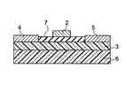
図1を参照すると、本発明の第1の実施の形態として窒化物半導体MIS型電界効果トランジスタの断面図が示されている。
(First embodiment)
Referring to FIG. 1, a cross-sectional view of a nitride semiconductor MIS field effect transistor is shown as a first embodiment of the present invention.
窒化物半導体3の表面にはソース電極4およびドレイン電極5が形成されている。このソース電極4とドレイン電極5間の窒化物半導体3の表面上には、アモルファス状態の、窒素を含むアルミニウムの酸化物7が設けられ、その上にゲート電極2が形成されている。
A
かかる窒化物半導体MIS型電界効果トランジスタにおいては、アモルファス状態の、窒素を含むアルミニウムの酸化物7がゲートの絶縁膜となっているので、窒化アルムニウム(AlN)結晶をゲート絶縁膜に用いた場合に問題となった結晶欠陥に起因するゲートリーク電流は発生しない。また、絶縁膜のエネルギーバンドギャップ値も7から9eVの範囲にあり窒化物半導体のエネルギーバンドギャップ値(例えばAl組成0.3のAlGaNで4.1eV)より十分高くSiN(エネルギーバンドギャップ値5eV)をゲート絶縁膜として用いた時に問題となった窒化物半導体の伝導帯からSiN絶縁膜の伝導帯へ電子が流れ込むゲートリーク電流の発生もない。更に、窒素を含むアルミニウムの酸化物7がゲートの絶縁膜となっているのでSiO2あるいはAl2O3等の絶縁膜と窒化物半導体3との界面に発生する界面準位も小さい。
In such a nitride semiconductor MIS field effect transistor, the
従って、図3に示すように、ゲートリーク電流の小さく高電圧動作が可能であり、また、図4に示すようにドレイン電流の変動が少なくなるという効果がもたらされる。 Therefore, as shown in FIG. 3, the gate leakage current is small and a high voltage operation is possible, and as shown in FIG. 4, the drain current fluctuation is reduced.
本発明による窒素を含むアルミニウムの酸化物をゲート絶縁膜に用いることにより、ゲートリーク電流および絶縁膜/窒化物半導体界面準位が低減されている。従って、高電圧動作可能となり高周波の出力特性が格段に向上する。 By using the oxide of aluminum containing nitrogen according to the present invention for the gate insulating film, the gate leakage current and the insulating film / nitride semiconductor interface state are reduced. Therefore, a high voltage operation becomes possible, and the high frequency output characteristics are remarkably improved.
このように第1の実施の形態の特徴は絶縁膜としてアモルファス状態の、窒素を含むアルミニウムの酸化物7を用いていることに有り、厚さとしては3nm以上20nm以下とし、酸素原子数/(窒素原子数+酸素原子数)の比率は0.4より大きく0.98以下に設定する。特に、リーク電流とFETのしきい値電圧の関係から膜厚に関しては7nm以上12nm以下が好ましい。
As described above, the feature of the first embodiment resides in the use of an
これは図5に示されるように、リーク電流が絶縁膜厚3nm以上で実用的に十分な2桁の低減があるからであり、20nm以上ではトランジスタのしきい値電圧が−12Vより深くなりバイアス電圧設定の点から実用的でなくなるからである。望ましくはリーク電流が10−7A/mmに抑えられる7nm以上しきい値電圧が−10Vより浅くなる12nm以下が好ましい。 This is because, as shown in FIG. 5, there is a practically sufficient two-digit reduction in leakage current when the insulating film thickness is 3 nm or more. When the current is 20 nm or more, the threshold voltage of the transistor becomes deeper than −12 V and bias is applied. This is because it is not practical in terms of voltage setting. Desirably, 7 nm or more at which the leakage current is suppressed to 10 −7 A / mm and 12 nm or less at which the threshold voltage is shallower than −10 V are preferable.
酸素原子数/(窒素原子数+酸素原子数)の比率は、図6に示すように、従来の窒化アルムニウム(AlN)におけるリーク電流が急激に低減できる0.4より大きいが必要で、望ましくは低いゲートリーク電流安定して得られる0.6以上が好ましい。酸素原子数/(窒素原子数+酸素原子数)の比率は界面準位の発生が少なくドレイン電流の変動の少ない0.95以下が必要で安定して低い界面準位が得られる0.90が望ましい。 As shown in FIG. 6, the ratio of the number of oxygen atoms / (number of nitrogen atoms + number of oxygen atoms) needs to be larger than 0.4, which can reduce the leakage current in the conventional aluminium nitride (AlN) rapidly. It is preferably 0.6 or more which can be obtained stably with a low gate leakage current. The ratio of the number of oxygen atoms / (the number of nitrogen atoms + the number of oxygen atoms) is 0.90 or less, in which the generation of interface states is small and the drain current does not fluctuate less than 0.95. desirable.
次に、図7を参照して、第1の実施の形態に係る窒化物半導体MIS型電界効果トランジスタの第1の製造方法について説明する。 Next, a first manufacturing method of the nitride semiconductor MIS field effect transistor according to the first embodiment will be described with reference to FIG.
始めに、基板6上に結晶成長により窒化物半導体3を形成した後、表面に窒化アルムニウム(AlN)8を成長する(図7(a))。窒化アルムニウム(AlN)8は連続的に成長される場合と一度大気中に取り出された後、別の成長装置で成長される場合がある。次に、窒化アルムニウム(AlN)8を酸化して窒素を含むアルミニウムの酸化物7を形成する(図7(b))。次に、窒素を含むアルミニウムの酸化物7の一部を開口して、窒化物半導体3とオーミック接触を形成するソース電極4及びドレイン電極5を形成する(図7(c))。最後に、窒素を含むアルミニウムの酸化物7上にゲート電極2を形成する(図7(d))。
First, after the
本実施の形態の製造方法では結晶成長で成膜した窒化アルムニウム(AlN)8を酸化して窒素を含むアルミニウムの酸化物7を形成しているため、絶縁膜/窒化物半導体界面がプロセス工程中に大気に暴露されておらず、表面汚染等影響が無いため界面準位の発生を特に制御性良く抑制できる。従って、ドレイン電流が動作中に変動することが無く安定して動作する利点が得られる(図3参照)。
In the manufacturing method of the present embodiment, aluminum oxide (AlN) 8 formed by crystal growth is oxidized to form
次に、具体的な実施例を用いて本実施の形態を説明する。 Next, this embodiment will be described using specific examples.
基板6として高抵抗SiC基板を用い、窒化物半導体3としてAlNバッファ層4nm,GaN層2000nm,AlGaN層(Al組成比0.25,厚さ30nm)を形成した。窒素を含むアルミニウムの酸化物7としてAlNを8nm成長し後、950℃の酸素雰囲気中で40分間熱処理することによりAlNを酸化してAlON膜(酸素原子数/(酸素原子数+窒素原子数)の元素の比率0.92)を形成した。その後、レジストをマスクにAlON膜を燐酸エッチング液にて除去してソース電極4、ドレイン電極5としてTi,Alを連続して蒸着した。その後、窒素雰囲気中650℃で熱処理することによりオーミックコンタクトを形成した。その後、ゲート電極2としてNi,Auを蒸着、リフトオフして形成した。
A high resistance SiC substrate was used as the
次に、図8を参照して、第1の実施の形態に係る窒化物半導体MIS型電界効果トランジスタの第2の製造方法を説明する。 Next, a second manufacturing method of the nitride semiconductor MIS field effect transistor according to the first embodiment will be described with reference to FIG.
始めに、基板6上に結晶成長により窒化物半導体3を形成した後、窒素を含むアルミニウムの酸化物7をスパッタ、CVD法等を用いて形成する(図8(a))。次に、窒素を含むアルミニウムの酸化物7の一部を開口して、窒化物半導体3とオーミック接触を形成するソース電極4及びドレイン電極5を形成する(図8(b))。最後に、窒素を含むアルミニウムの酸化物7上にゲート電極2を形成する(図8(c))。
First, after the
本実施の形態の製造方法では、スパッタ法、気相成長法を用いて窒素を含むアルミニウムの酸化物7を形成しているため、成長温度(約1000℃)に比較して電極等の劣化がない低い温度(400℃)以下の一回の成膜で窒素を含むアルミニウムの酸化物7が形成できる。このため、プロセス工程およびプロセス設備が簡略化できる。本実施の形態では窒素を含むアルミニウムの酸化物7を成膜する前に、界面準位低減のため窒化物半導体表面の清浄化工程を取り入れることが望ましい。
In the manufacturing method of this embodiment, since the
具体的な実施例を用いて本実施の形態を説明する。基板6として高抵抗SiC基板を用い、窒化物半導体3としてAlNバッファ層4nm,GaN層2000nm,AlGaN層(Al組成比0.25,厚さ30nm)を形成した。窒素を含むアルミニウムの酸化物7としてスパッタ装置にてAl2O3をアルゴン、窒素混合ガスでスパッタ蒸着することにより酸素原子数/(酸素原子数+窒素原子数)の元素の比率0.8のAlON膜、厚さ10nmを形成した。その後、レジストをマスクにAlON膜を燐酸エッチング液にて除去してソース電極4、ドレイン電極5としてTi,Alを連続して蒸着した。その後、窒素雰囲気中650℃で熱処理することによりオーミックコンタクトを形成した。その後、ゲート電極2としてNi,Auを蒸着、リフトオフして形成した。
This embodiment will be described using specific examples. A high resistance SiC substrate was used as the
次に、図9を参照して、第1の実施の形態に係る窒化物半導体MIS型電界効果トランジスタの第3の製造方法を説明する。 Next, a third manufacturing method of the nitride semiconductor MIS field effect transistor according to the first embodiment will be described with reference to FIG.
始めに、基板6上に結晶成長により窒化物半導体3を形成した後、窒化物半導体3とオーミック接触を形成するソース電極4、ドレイン電極5を形成する(図9(a))。次に、窒素を含むアルミニウムの酸化物7をスパッタ、CVD法等を用いて形成する窒素を含むアルミニウムの酸化物7形成する(図9(b))。次に、窒素を含むアルミニウムの酸化物7上にゲート電極2を形成する(図9(c))。最後に、ソース電極4及びドレイン電極5の一部を開口して外部との電気的接続を可能とする(図9(d))。
First, after the
本実施の形態の製造方法では、ソース電極4及びドレイン電極5のゲート電極2側の端が窒素を含むアルミニウムの酸化物7で隙間無く保護されているので電極の長期的な劣化が無く信頼性が高いトランジスタが実現できる。
In the manufacturing method of the present embodiment, the ends of the
具体的な実施例を用いて本実施の形態を説明する。 This embodiment will be described using specific examples.
基板6として高抵抗SiC基板を用い、窒化物半導体3としてAlNバッファ層4nm,GaN層2000nm,AlGaN層(Al組成比0.25,厚さ30nm)を形成した。次に、ソース電極4、ドレイン電極5としてTi,Alを連続して蒸着して、窒素雰囲気中650℃で熱処理することによりオーミックコンタクトを形成した。その後、窒素を含むアルミニウムの酸化物7としてスパッタ装置にてAl2O3をアルゴン、窒素混合ガスでスパッタ蒸着することにより、厚さ10nmのAlON(酸素原子数/(酸素原子数+窒素原子数)の原子の比率0.85)を形成した。その後、ゲート電極2としてNi,Auを蒸着、リフトオフして形成した。
A high resistance SiC substrate was used as the
(第2の実施の形態)
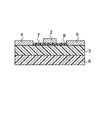
上記実施の形態において、電極間の窒化物半導体表面を被う絶縁膜を窒素を含むアルミニウムの酸化物7と第2の絶縁膜で構成することができる。そのための構成を、第2の実施の形態として図10(a)示す。
(Second Embodiment)
In the above embodiment, the insulating film covering the surface of the nitride semiconductor between the electrodes can be composed of the
本第2の実施の形態では、界面準位が低いことを必要とするゲート電極2の直下とその周辺部分を界面準位が低いことを特徴とする窒素を含むアルミニウムの酸化物7で被い、ソース電極4及びドレイン電極5までの残りの窒化物半導体表面を高いドレイン耐圧特性を示す表面保護膜8で被う。
In this second embodiment, the
本実施の形態では、電極間の絶縁膜を窒素を含むアルミニウムの酸化物7単層にした場合より高い電圧まで電界効果トランジスタを動作させることが可能となり、第1の実施の形態よりさらに高い出力特性が得られるという格別な効果を奏する。
In the present embodiment, it becomes possible to operate the field effect transistor to a higher voltage than when the insulating film between the electrodes is a single layer of
また、本実施の形態の電極間の絶縁膜の構成において、窒素を含むアルミニウムの酸化物7と表面保護膜8で構成する形態を、図10(b)に示すように、高い電圧が加わるゲート電極2とドレイン電極5の間のみに適用されるように変更してもよい。
Further, in the structure of the insulating film between the electrodes in this embodiment mode, a form in which the
次に、図11を参照して、第2の実施の形態に係る窒化物半導体MIS型電界効果トランジスタの製造方法について説明する。 Next, a method for manufacturing the nitride semiconductor MIS field effect transistor according to the second embodiment will be described with reference to FIG.
始めに、基板6上に結晶成長により窒化物半導体3を形成した表面に窒素を含むアルミニウムの酸化物7を第1の実施の形態の第1あるいは第2の製造方法と同様な手法で形成する(図11(a))。次に、窒素を含むアルミニウムの酸化物7をゲート電極7の直下とその周辺部に相当する領域のみ残してその他を除去する(図11(b))。
First, an
続いて、窒化物半導体3とオーミック接触を形成するソース電極4及びドレイン電極5を形成する(図13(c))。次に、窒素を含むアルミニウムの酸化物7上にゲート電極2を形成する(図11(d))。最後に表面保護膜8で表面を被い、ソース電極4、ドレイン電極5及びゲート電極2の電流取り出し領域の表面保護膜8を除去する。
Subsequently, the
具体的な実施例を用いて本実施の形態を説明する。 This embodiment will be described using specific examples.
基板6として高抵抗SiC基板を用い、窒化物半導体3としてAlNバッファ層4nm,GaN層2000nm,AlGaN層(Al組成比0.25,厚さ30nm)を形成した。窒素を含むアルミニウムの酸化物7としてスパッタ装置にてAl2O3をアルゴン、窒素混合ガスでスパッタ蒸着することにより厚さ10nmのAlON膜(酸素原子数/(酸素原子数+窒素原子数)の原子の比率0.8)を形成した。その後、レジストをマスクとして使用して、AlON膜のゲート電極2の周辺部以外を燐酸エッチング液にて除去した。
A high resistance SiC substrate was used as the
AlON膜開口部中のソース電極4、ドレイン電極5部分にTi,Alを連続して蒸着し、窒素雰囲気中650℃で熱処理することによりオーミックコンタクトを形成した。AlON膜上にはゲート電極2としてNi,Auを蒸着、リフトオフして形成した。最後に、全体に表面保護膜8としてSiO2を200nm形成し電流取り出し領域の電極部を開口した。本構造を用いることで、MISFETは80Vまで動作可能となった。
Ti and Al were continuously deposited on the
(第3の実施の形態)
上記の電極間の絶縁膜を窒素を含むアルミニウムの酸化物7と表面保護膜8で構成する実施の形態において、ゲート電極直下のみを窒素を含むアルミニウムの酸化物7で被うことができる。そのための構成を、第3の実施の形態として図12に示す。
(Third embodiment)
In the embodiment in which the insulating film between the electrodes is composed of the
電極間の絶縁膜を窒素を含むアルミニウムの酸化物7と第2の絶縁膜で構成する本第3の実施の形態では、界面準位が低いことを必要とするゲート電極2の直下のみを窒素を含むアルミニウムの酸化物7で被い、ソース電極4及びドレイン電極5までの窒化物半導体表面を高い耐圧特性を示す表面保護膜8で被う。
In the third embodiment in which the insulating film between the electrodes is composed of the
本実施の形態では、電極間の絶縁膜を窒素を含むアルミニウムの酸化物7単層あるいは表面保護膜8との2層構造にした場合より、表面保護膜8単層のほうが、電界効果トランジスタとして高い電圧まで安定して動作してより高い出力を可能とするという格別な効果を奏する。
In the present embodiment, the single layer of the surface
また、本実施の形態の電極間の絶縁膜の構成において、窒素を含むアルミニウムの酸化物7と第2の絶縁膜の2種類の膜で構成する形態を、高い電圧が加わるゲート電極2とドレイン電極5間のみに適用されるように変更してもよい。
In addition, in the structure of the insulating film between the electrodes in this embodiment mode, a structure in which two kinds of films, that is, an
次に、図13を参照して、第3の実施の形態に係る窒化物半導体MIS型電界効果トランジスタの製造方法について説明する。 Next, with reference to FIG. 13, a method for manufacturing the nitride semiconductor MIS field effect transistor according to the third embodiment will be described.
始めに、基板6上に結晶成長により窒化物半導体3を形成した表面に窒素を含むアルミニウムの酸化物7を第1の実施の形態の第1あるいは第2の製造方法と同様な手法で形成する(図12(a))。次に、ゲート電極2を蒸着あるいはスパッタ法を用いて形成する(図12(b))。続いて、窒素を含むアルミニウムの酸化物7をゲート電極をマスクとしてエッチング除去した後、ソース電極4及びドレイン電極5を窒化物半導体3の表面に形成する(図12(c))。最後に、表面保護膜8で表面を被い、ソース電極4、ドレイン電極5及びゲート電極2の電流取り出し領域の表面保護膜8を除去する(図12(d))。
First, an
具体的な実施例を用いて本実施の形態を説明する。 This embodiment will be described using specific examples.
基板6として高抵抗SiC基板を用い、窒化物半導体3としてAlNバッファ層4nm,GaN層2000nm,AlGaN層(Al組成比0.25,厚さ30nm)を形成した。窒素を含むアルミニウムの酸化物7としてスパッタ装置にてAl2O3をアルゴン、窒素混合ガスでスパッタ蒸着することにより厚さ10nmのAlON膜(酸素原子数/(酸素原子数+窒素原子数)の原子の比率0.8)を形成した。AlON膜上にはゲート電極2としてNi,Auを蒸着、リフトオフして形成した。その後、ゲート電極2をマスクとして使用して、AlON膜を燐酸エッチング液にて除去した。ソース電極4、ドレイン電極5部分にTi,Alを連続して蒸着し、窒素雰囲気中650℃で熱処理することによりオーミックコンタクトを形成した。最後に、全体に表面保護膜8としてSiO2を200nm形成し電流取り出し領域の電極部を開口した。本構造を用いることでMISFETは100Vまで動作可能となった。
A high resistance SiC substrate was used as the
(第4の実施の形態)
上記各実施の形態において、ゲート電極下に窒素を含むアルミニウムの酸化物7の単層を用いたが、窒素を含むアルミニウムの酸化物7と窒化物半導体3の間に窒化アルミニウム(AlN)9を挿入した構造によって構成することができる。そのための構成を、第4の実施の形態として図14に示す。
(Fourth embodiment)
In each of the above embodiments, a single layer of
窒化物半導体3の表面にはソース電極4及びドレイン電極5が形成されている。このソース電極4とドレイン電極5間の窒化物半導体3の表面上には、窒化アルミニウム(AlN)9とアモルファス状態の、窒素を含むアルミニウムの酸化物7が積層して設けられ、その上にゲート電極2が形成されている。
A
かかる窒化物半導体MIS型電界効果トランジスタにおいては、窒化アルミニウム(AlN)9とアモルファス状態の、窒素を含むアルミニウムの酸化物7の2層膜がゲート2の絶縁膜となっているので、窒化アルムニウム(AlN)9結晶を単層としてゲート絶縁膜に用いた場合に問題となった結晶欠陥に起因するゲートリーク電流は発生しない。
In such a nitride semiconductor MIS field effect transistor, the two-layer film of
また、絶縁膜のエネルギーバンドギャップ値も7から9eVの範囲にあり窒化物半導体のエネルギーバンドギャップ値(例えばAl組成0.3のAlGaNで4.1eV)より十分高くSiN(エネルギーバンドギャップ値5eV)をゲート絶縁膜として用いた時に問題となった窒化物半導体の伝導帯からSiN絶縁膜の伝導帯へ電子が流れ込むゲートリーク電流の発生もない。
Also, the energy band gap value of the insulating film is in the range of 7 to 9 eV, which is sufficiently higher than the energy band gap value of nitride semiconductors (for example, 4.1 eV for AlGaN having an Al composition of 0.3) (energy
更に、窒化物半導体3,窒化アルミニウム9,窒素を含むアルミニウムの酸化物7が順次ヘテロ界面を形成しており,電流が流れる窒化物半導体3と窒化アルミニウム(AlN)9の界面準位は窒化物結晶で構成されているため界面準位密度は最も小さくなる。
Further, the
更に、窒化アルミニウム(AlN)9と窒素を含むアルミニウムの酸化物7の界面に発生する界面準位もSiO2あるいはAl2O3等の絶縁膜を窒素を含むアルミニウムの酸化物7の代わりに用いた場合よりも大幅に低減できる。これは絶縁膜/窒化アルミニウム(AlN)9界面を形成する際、窒素を含むアルミニウムの酸化物7を用いることにより窒化アルミニウム(AlN)9からの窒素の脱離を抑制して、窒素抜けにより発生する界面準位密度を低く抑えるからである。
Furthermore, an interface state generated at the interface between aluminum nitride (AlN) 9 and nitrogen-containing
従って、ゲートリーク電流の小さく(図2参照)、高電圧動作が可能でドレイン電流の変動が少なくなる(図3参照)という効果がもたらされる。 Therefore, the gate leakage current is small (see FIG. 2), high voltage operation is possible, and the drain current fluctuation is small (see FIG. 3).
本発明による窒素を含むアルミニウムの酸化物のゲート絶縁膜の存在により、ゲートリーク電流および絶縁膜/窒化物半導体界面準位が低減されている。従って、高電圧動作可能となり高周波の出力特性が格段に向上する。 The presence of the nitrogen-containing aluminum oxide gate insulating film according to the present invention reduces the gate leakage current and the insulating film / nitride semiconductor interface state. Therefore, a high voltage operation becomes possible, and the high frequency output characteristics are remarkably improved.
このように、第4の実施の形態の特徴は絶縁膜として、窒素を含むアルミニウムの酸化物7と窒化アルミニウム9の2層膜を用いていることにある。この場合、窒化アルミニウム(AlN)9の厚さは4nm以下であり、窒素を含むアルミニウムの酸化物7の厚さとしては3nm以上16nm以下とし、酸素原子数/(酸素原子数+窒素原子数)の比率は0.4より大きく0.98以下に設定する。
As described above, the fourth embodiment is characterized in that a two-layer film of aluminum-containing
特に、リーク電流とFETのしきい値電圧の関係から膜厚に関しては7nm以上11nm以下が好ましい。これは図16に示されるようにリーク電流が絶縁膜厚3nm以上で実用的に十分な2桁の低減があるからであり、16nm以上ではトランジスタのしきい値電圧が−12Vより深くなりバイアス電圧設定の点から実用的でなくなるからである。望ましくは、リーク電流が10−10A/mmに抑えられる7nm以上しきい値電圧が−10Vより浅くなる11nm以下が好ましい。 In particular, from the relationship between the leakage current and the threshold voltage of the FET, the film thickness is preferably 7 nm or more and 11 nm or less. This is because, as shown in FIG. 16, there is a practically sufficient two-digit reduction in leakage current when the insulation film thickness is 3 nm or more. When the thickness is 16 nm or more, the threshold voltage of the transistor becomes deeper than −12 V and the bias voltage is increased. This is because it is not practical in terms of setting. Desirably, 7 nm or more at which the leakage current is suppressed to 10 −10 A / mm and 11 nm or less at which the threshold voltage is shallower than −10 V are preferable.
酸素原子数/(酸素原子数+窒素原子数)の比率は、第1の実施の形態の図5に示すように従来の窒化アルムニウム(AlN)におけるリーク電流が急激に低減できる0.4より大きいことが必要で望ましくは低いゲートリーク電流安定して得られる0.6以上が望ましい。酸素原子数/(酸素原子数+窒素原子数)の比率は界面準位の発生が少なくドレイン電流の変動の少ない0.95以下が必要で安定して低い界面準位が得られるの0.90が望ましい。 The ratio of the number of oxygen atoms / (the number of oxygen atoms + the number of nitrogen atoms) is larger than 0.4, which can rapidly reduce the leakage current in the conventional aluminum nitride (AlN) as shown in FIG. 5 of the first embodiment. It is necessary, and preferably 0.6 or more, which can be obtained stably with a low gate leakage current. The ratio of the number of oxygen atoms / (the number of oxygen atoms + the number of nitrogen atoms) needs to be 0.95 or less with little generation of interface states and little fluctuation of drain current, and a stable low interface state can be obtained. Is desirable.
次に、図15を参照して、第4の実施の形態に係る窒化物半導体MIS型電界効果トランジスタの製造方法について説明する。 Next, with reference to FIG. 15, a method for manufacturing the nitride semiconductor MIS field effect transistor according to the fourth embodiment will be described.
始めに、基板6上に結晶成長により窒化物半導体3を形成した後、表面に窒化アルムニウム(AlN)9を成長する(図15(a))。窒化アルムニウム(AlN)9は連続的に成長される場合と一度大気中に取り出された後、別の成長装置で成長される場合がある。次に、窒化アルムニウム(AlN)9の表面層を酸化して窒素を含むアルミニウムの酸化物7を形成する(図15(b))。このとき窒化アルムニウム(AlN)9の層を厚さ4nm以下残して酸化を終了する。次に、窒素を含むアルミニウムの酸化物7及び窒化アルムニウム(AlN)9の一部を開口して、窒化物半導体3とオーミック接触を形成するソース電極4及びドレイン電極5を形成する(図15(c))。最後に、窒素を含むアルミニウムの酸化物7上にゲート電極2を形成する(図15(d))。
First, after the
本実施の形態の製造方法では、結晶成長で成膜した窒化アルムニウム(AlN)9を4nm以下残して表面側を酸化して窒素を含むアルミニウムの酸化物7を形成しているため、絶縁膜/窒化物半導体界面がプロセス工程中に大気に暴露されておらず、表面汚染等影響が無いため界面準位の発生を特に制御性良く抑制できる。
In the manufacturing method of the present embodiment,
また、従来のAl2O3、SiO2等の酸化膜を用いず窒素を含むアルミニウムの酸化物7を用いることにより窒化アルミニウム(AlN)9からの窒素の脱離を抑制して、窒素抜けにより発生する界面準位密度も低く抑える特徴がある。従って、ドレイン電流が動作中に変動することが無く安定して動作する利点が得られる(図17参照)。
Further, by using an
次に、具体的な実施例を用いて本実施の形態を説明する。 Next, this embodiment will be described using specific examples.
基板6として高抵抗SiC基板を用い、窒化物半導体3としてAlNバッファ層5nm,GaN層2000nm,AlGaN層(Al組成比0.25,厚さ30nm)を形成した。窒素を含むアルミニウムの酸化物7としてAlNを8nm成長し後、950℃の酸素雰囲気中で30分間熱処理することによりAlNの上層を酸化してAlON(酸素原子濃度85%,厚さ5nm)/AN(厚さ3nm)の2層膜を形成した。
A high resistance SiC substrate was used as the
その後、レジストをマスクとして使用して、AlON/AlNの2層膜を燐酸エッチング液にて除去してソース電極4、ドレイン電極5としてTi,Alを連続して蒸着した。その後、窒素雰囲気中650℃で熱処理することによりオーミックコンタクトを形成した。その後、ゲート電極2としてNi,Auを蒸着、リフトオフして形成した。
Thereafter, using the resist as a mask, the two-layer film of AlON / AlN was removed with a phosphoric acid etching solution, and Ti and Al were successively deposited as the
なお、第4の実施の形態では窒素を含むアルミニウムの酸化物7と窒化物半導体3の間に窒化アルミニウム(AlN)9を挿入した層が、ソース電極4とドレイン電極5間の全領域を被った場合を説明したが、第2あるいは3の実施の形態と同様に、2層膜がゲート2の近傍のみに存在して第2の絶縁膜によってソース電極4とドレイン電極5間の残りの領域が被われる構造を用いれば、動作電圧をさらに高める効果がある。
In the fourth embodiment, a layer in which aluminum nitride (AlN) 9 is inserted between
1 ゲート絶縁膜
2 ゲート電極
3 窒化物半導体
4 ソース電極
5 ドレイン電極
6 基板
7 窒素を含むアルミの酸化物(AlON)
8 表面保護膜
9 窒化アルミニウム(AlN)
DESCRIPTION OF
8 Surface
Claims (5)
前記窒化物半導体を形成した後、
前記窒化物半導体表面に、窒素を含むアルミニウムの酸化物をスパッタ法または気相成長法を用いて成膜し、前記ゲート絶縁膜をアモルファス状態の単一層に形成し、
前記ゲート絶縁膜の厚さが3nm以上で20nm以下であり、
前記ゲート絶縁膜の酸素原子数と窒素原子数の比(酸素原子数/(酸素原子数+窒素原子数))が0.4より大きく0.95以下であることを特徴とする窒化物半導体MIS型電界効果トランジスタの製造方法。 In a method of manufacturing a nitride semiconductor MIS field effect transistor having a gate insulating film between a nitride semiconductor surface and a gate electrode,
After forming the nitride semiconductor,
On the nitride semiconductor surface, an oxide of aluminum containing nitrogen is formed using a sputtering method or a vapor phase growth method, and the gate insulating film is formed into a single layer in an amorphous state.
A thickness of the gate insulating film is 3 nm or more and 20 nm or less;
The ratio of the number of oxygen atoms to the number of nitrogen atoms (number of oxygen atoms / (number of oxygen atoms + number of nitrogen atoms)) of the gate insulating film is greater than 0.4 and less than or equal to 0.95. Type field effect transistor manufacturing method.
ゲート絶縁膜端からドレイン電極端までの窒化物半導体表面は、窒素を含むアルミニウムの酸化物以外の第2の絶縁膜で被われていることを特徴とする請求項1に記載の窒化物半導体MIS型電界効果トランジスタの製造方法。 The gate insulating film covers the nitride semiconductor surface directly under and around the gate electrode,
2. The nitride semiconductor MIS according to claim 1 , wherein a surface of the nitride semiconductor from the end of the gate insulating film to the end of the drain electrode is covered with a second insulating film other than an oxide of aluminum containing nitrogen. Type field effect transistor manufacturing method.
Priority Applications (1)
| Application Number | Priority Date | Filing Date | Title |
|---|---|---|---|
| JP2003421001A JP4741792B2 (en) | 2003-12-18 | 2003-12-18 | Manufacturing method of nitride semiconductor MIS type field effect transistor |
Applications Claiming Priority (1)
| Application Number | Priority Date | Filing Date | Title |
|---|---|---|---|
| JP2003421001A JP4741792B2 (en) | 2003-12-18 | 2003-12-18 | Manufacturing method of nitride semiconductor MIS type field effect transistor |
Publications (2)
| Publication Number | Publication Date |
|---|---|
| JP2005183597A JP2005183597A (en) | 2005-07-07 |
| JP4741792B2 true JP4741792B2 (en) | 2011-08-10 |
Family
ID=34782359
Family Applications (1)
| Application Number | Title | Priority Date | Filing Date |
|---|---|---|---|
| JP2003421001A Expired - Lifetime JP4741792B2 (en) | 2003-12-18 | 2003-12-18 | Manufacturing method of nitride semiconductor MIS type field effect transistor |
Country Status (1)
| Country | Link |
|---|---|
| JP (1) | JP4741792B2 (en) |
Families Citing this family (17)
| Publication number | Priority date | Publication date | Assignee | Title |
|---|---|---|---|---|
| JP4945979B2 (en) * | 2005-09-16 | 2012-06-06 | 富士通株式会社 | Nitride semiconductor field effect transistor |
| JP2008103408A (en) * | 2006-10-17 | 2008-05-01 | Furukawa Electric Co Ltd:The | Nitride compound semiconductor transistor and manufacturing method thereof |
| JP2008198787A (en) * | 2007-02-13 | 2008-08-28 | Rohm Co Ltd | GaN-BASED SEMICONDUCTOR DEVICE |
| JP5332113B2 (en) | 2007-02-15 | 2013-11-06 | 富士通株式会社 | Semiconductor device and manufacturing method thereof |
| JP2008218846A (en) * | 2007-03-06 | 2008-09-18 | Rohm Co Ltd | Nitride semiconductor element and manufacturing method of nitride semiconductor element |
| JP4963455B2 (en) * | 2007-09-04 | 2012-06-27 | 国立大学法人北海道大学 | Method and apparatus for forming an insulating film on the surface of a semiconductor substrate |
| WO2011027871A1 (en) * | 2009-09-04 | 2011-03-10 | 住友化学株式会社 | Semiconductor substrate, field effect transistor, integrated circuit, and method for producing semiconductor substrate |
| JP2013140866A (en) | 2012-01-04 | 2013-07-18 | Renesas Electronics Corp | Semiconductor device, and method of manufacturing the same |
| JP2014110402A (en) * | 2012-12-04 | 2014-06-12 | Rohm Co Ltd | Semiconductor device |
| TWI609490B (en) | 2013-05-31 | 2017-12-21 | 住友化學股份有限公司 | Semiconductor substrate, method of producing semiconductor and electronic device |
| KR102392059B1 (en) * | 2013-07-29 | 2022-04-28 | 삼성전자주식회사 | Semiconductor device and method of fabricating the same |
| US9553181B2 (en) * | 2015-06-01 | 2017-01-24 | Toshiba Corporation | Crystalline-amorphous transition material for semiconductor devices and method for formation |
| JP6594272B2 (en) * | 2016-09-02 | 2019-10-23 | 株式会社東芝 | Semiconductor device and manufacturing method thereof |
| JP6773629B2 (en) | 2017-11-22 | 2020-10-21 | 株式会社東芝 | Semiconductor devices, inverter circuits, drives, vehicles, elevators, power supply circuits, and computers |
| JP6728123B2 (en) | 2017-11-22 | 2020-07-22 | 株式会社東芝 | Semiconductor device, power supply circuit, and computer |
| JP6945036B2 (en) * | 2018-05-24 | 2021-10-06 | ローム株式会社 | Semiconductor device |
| JP7185225B2 (en) * | 2018-11-22 | 2022-12-07 | 株式会社豊田中央研究所 | Semiconductor device and method for manufacturing semiconductor device |
Family Cites Families (7)
| Publication number | Priority date | Publication date | Assignee | Title |
|---|---|---|---|---|
| JPS6423571A (en) * | 1987-07-20 | 1989-01-26 | Nec Corp | Semiconductor element |
| JPS6482671A (en) * | 1987-09-25 | 1989-03-28 | Nec Corp | Manufacture of mis field-effect transistor |
| JPH10223901A (en) * | 1996-12-04 | 1998-08-21 | Sony Corp | Field effect transistor and manufacture of the same |
| JP4224737B2 (en) * | 1999-03-04 | 2009-02-18 | ソニー株式会社 | Semiconductor element |
| WO2003032397A2 (en) * | 2001-07-24 | 2003-04-17 | Cree, Inc. | INSULTING GATE AlGaN/GaN HEMT |
| WO2003026019A1 (en) * | 2001-09-12 | 2003-03-27 | Nec Corporation | Semiconductor device and production method therefor |
| JP2004165387A (en) * | 2002-11-12 | 2004-06-10 | Furukawa Electric Co Ltd:The | Gan-based field effect transistor |
-
2003
- 2003-12-18 JP JP2003421001A patent/JP4741792B2/en not_active Expired - Lifetime
Also Published As
| Publication number | Publication date |
|---|---|
| JP2005183597A (en) | 2005-07-07 |
Similar Documents
| Publication | Publication Date | Title |
|---|---|---|
| JP4741792B2 (en) | Manufacturing method of nitride semiconductor MIS type field effect transistor | |
| JP5200936B2 (en) | Field effect transistor and manufacturing method thereof | |
| KR100859060B1 (en) | Semiconductor device and method for fabricating the same | |
| TWI546864B (en) | Enhancement-mode gan mosfet with low leakage current and improved reliability | |
| US7525122B2 (en) | Passivation of wide band-gap based semiconductor devices with hydrogen-free sputtered nitrides | |
| TWI313060B (en) | Feild effect transisitor and fabricating method thereof | |
| JP5347228B2 (en) | Field effect transistor | |
| JP2006278812A (en) | Semiconductor device, its fabrication process, substrate for manufacturing semiconductor device, and its production process | |
| US20050017272A1 (en) | Semiconductor device and production method therefor | |
| JP5401775B2 (en) | Compound semiconductor device and manufacturing method thereof | |
| JP5998446B2 (en) | Compound semiconductor device and manufacturing method thereof | |
| JP5332113B2 (en) | Semiconductor device and manufacturing method thereof | |
| JP4134575B2 (en) | Semiconductor device and manufacturing method thereof | |
| JP2012044003A (en) | Semiconductor device and manufacturing method of the same | |
| JP2009088440A (en) | Semiconductor device and its manufacturing method | |
| JP2006216918A (en) | Manufacturing method of semiconductor device | |
| US20180190790A1 (en) | Nitride semiconductor device and method for manufacturing the same | |
| JP2013168433A (en) | Nitride semiconductor device and method of manufacturing nitride semiconductor device | |
| WO2023045046A1 (en) | Gold-free ohmic contact electrode, semiconductor device, and radio-frequency device and manufacturing method therefor | |
| JP5101143B2 (en) | Field effect transistor and manufacturing method thereof | |
| JP2000150792A (en) | Semiconductor device and its manufacture | |
| JP5072482B2 (en) | Method for manufacturing silicon carbide semiconductor device | |
| US9741859B2 (en) | Semiconductor device with graphene layer as channel | |
| JP2004247709A (en) | Semiconductor device and manufacturing method therefor | |
| JP6687831B2 (en) | Compound semiconductor device and manufacturing method thereof |
Legal Events
| Date | Code | Title | Description |
|---|---|---|---|
| A621 | Written request for application examination |
Free format text: JAPANESE INTERMEDIATE CODE: A621 Effective date: 20061109 |
|
| A977 | Report on retrieval |
Free format text: JAPANESE INTERMEDIATE CODE: A971007 Effective date: 20080725 |
|
| A131 | Notification of reasons for refusal |
Free format text: JAPANESE INTERMEDIATE CODE: A131 Effective date: 20100127 |
|
| A521 | Request for written amendment filed |
Free format text: JAPANESE INTERMEDIATE CODE: A523 Effective date: 20100326 |
|
| A131 | Notification of reasons for refusal |
Free format text: JAPANESE INTERMEDIATE CODE: A131 Effective date: 20101027 |
|
| A521 | Request for written amendment filed |
Free format text: JAPANESE INTERMEDIATE CODE: A523 Effective date: 20101224 |
|
| A131 | Notification of reasons for refusal |
Free format text: JAPANESE INTERMEDIATE CODE: A131 Effective date: 20110119 |
|
| A521 | Request for written amendment filed |
Free format text: JAPANESE INTERMEDIATE CODE: A523 Effective date: 20110318 |
|
| TRDD | Decision of grant or rejection written | ||
| A01 | Written decision to grant a patent or to grant a registration (utility model) |
Free format text: JAPANESE INTERMEDIATE CODE: A01 Effective date: 20110413 |
|
| A01 | Written decision to grant a patent or to grant a registration (utility model) |
Free format text: JAPANESE INTERMEDIATE CODE: A01 |
|
| A61 | First payment of annual fees (during grant procedure) |
Free format text: JAPANESE INTERMEDIATE CODE: A61 Effective date: 20110509 |
|
| R150 | Certificate of patent or registration of utility model |
Ref document number: 4741792 Country of ref document: JP Free format text: JAPANESE INTERMEDIATE CODE: R150 Free format text: JAPANESE INTERMEDIATE CODE: R150 |
|
| FPAY | Renewal fee payment (event date is renewal date of database) |
Free format text: PAYMENT UNTIL: 20140513 Year of fee payment: 3 |
|
| R250 | Receipt of annual fees |
Free format text: JAPANESE INTERMEDIATE CODE: R250 |
|
| S531 | Written request for registration of change of domicile |
Free format text: JAPANESE INTERMEDIATE CODE: R313531 |
|
| R350 | Written notification of registration of transfer |
Free format text: JAPANESE INTERMEDIATE CODE: R350 |
|
| EXPY | Cancellation because of completion of term |