JP4735239B2 - Discharge lamp lighting device and image display device - Google Patents
Discharge lamp lighting device and image display device Download PDFInfo
- Publication number
- JP4735239B2 JP4735239B2 JP2005368957A JP2005368957A JP4735239B2 JP 4735239 B2 JP4735239 B2 JP 4735239B2 JP 2005368957 A JP2005368957 A JP 2005368957A JP 2005368957 A JP2005368957 A JP 2005368957A JP 4735239 B2 JP4735239 B2 JP 4735239B2
- Authority
- JP
- Japan
- Prior art keywords
- switching
- discharge lamp
- frequency
- switching element
- switching frequency
- Prior art date
- Legal status (The legal status is an assumption and is not a legal conclusion. Google has not performed a legal analysis and makes no representation as to the accuracy of the status listed.)
- Expired - Fee Related
Links
Images


Classifications
-
- H—ELECTRICITY
- H05—ELECTRIC TECHNIQUES NOT OTHERWISE PROVIDED FOR
- H05B—ELECTRIC HEATING; ELECTRIC LIGHT SOURCES NOT OTHERWISE PROVIDED FOR; CIRCUIT ARRANGEMENTS FOR ELECTRIC LIGHT SOURCES, IN GENERAL
- H05B41/00—Circuit arrangements or apparatus for igniting or operating discharge lamps
- H05B41/14—Circuit arrangements
- H05B41/26—Circuit arrangements in which the lamp is fed by power derived from DC by means of a converter, e.g. by high-voltage DC
- H05B41/28—Circuit arrangements in which the lamp is fed by power derived from DC by means of a converter, e.g. by high-voltage DC using static converters
- H05B41/288—Circuit arrangements in which the lamp is fed by power derived from DC by means of a converter, e.g. by high-voltage DC using static converters with semiconductor devices and specially adapted for lamps without preheating electrodes, e.g. for high-intensity discharge lamps, high-pressure mercury or sodium lamps or low-pressure sodium lamps
- H05B41/2881—Load circuits; Control thereof
- H05B41/2882—Load circuits; Control thereof the control resulting from an action on the static converter
-
- G—PHYSICS
- G03—PHOTOGRAPHY; CINEMATOGRAPHY; ANALOGOUS TECHNIQUES USING WAVES OTHER THAN OPTICAL WAVES; ELECTROGRAPHY; HOLOGRAPHY
- G03B—APPARATUS OR ARRANGEMENTS FOR TAKING PHOTOGRAPHS OR FOR PROJECTING OR VIEWING THEM; APPARATUS OR ARRANGEMENTS EMPLOYING ANALOGOUS TECHNIQUES USING WAVES OTHER THAN OPTICAL WAVES; ACCESSORIES THEREFOR
- G03B21/00—Projectors or projection-type viewers; Accessories therefor
- G03B21/14—Details
- G03B21/20—Lamp housings
- G03B21/2006—Lamp housings characterised by the light source
- G03B21/2026—Gas discharge type light sources, e.g. arcs
-
- H—ELECTRICITY
- H02—GENERATION; CONVERSION OR DISTRIBUTION OF ELECTRIC POWER
- H02M—APPARATUS FOR CONVERSION BETWEEN AC AND AC, BETWEEN AC AND DC, OR BETWEEN DC AND DC, AND FOR USE WITH MAINS OR SIMILAR POWER SUPPLY SYSTEMS; CONVERSION OF DC OR AC INPUT POWER INTO SURGE OUTPUT POWER; CONTROL OR REGULATION THEREOF
- H02M3/00—Conversion of DC power input into DC power output
- H02M3/02—Conversion of DC power input into DC power output without intermediate conversion into AC
- H02M3/04—Conversion of DC power input into DC power output without intermediate conversion into AC by static converters
- H02M3/10—Conversion of DC power input into DC power output without intermediate conversion into AC by static converters using discharge tubes with control electrode or semiconductor devices with control electrode
- H02M3/145—Conversion of DC power input into DC power output without intermediate conversion into AC by static converters using discharge tubes with control electrode or semiconductor devices with control electrode using devices of a triode or transistor type requiring continuous application of a control signal
- H02M3/155—Conversion of DC power input into DC power output without intermediate conversion into AC by static converters using discharge tubes with control electrode or semiconductor devices with control electrode using devices of a triode or transistor type requiring continuous application of a control signal using semiconductor devices only
- H02M3/156—Conversion of DC power input into DC power output without intermediate conversion into AC by static converters using discharge tubes with control electrode or semiconductor devices with control electrode using devices of a triode or transistor type requiring continuous application of a control signal using semiconductor devices only with automatic control of output voltage or current, e.g. switching regulators
- H02M3/157—Conversion of DC power input into DC power output without intermediate conversion into AC by static converters using discharge tubes with control electrode or semiconductor devices with control electrode using devices of a triode or transistor type requiring continuous application of a control signal using semiconductor devices only with automatic control of output voltage or current, e.g. switching regulators with digital control
-
- H—ELECTRICITY
- H05—ELECTRIC TECHNIQUES NOT OTHERWISE PROVIDED FOR
- H05B—ELECTRIC HEATING; ELECTRIC LIGHT SOURCES NOT OTHERWISE PROVIDED FOR; CIRCUIT ARRANGEMENTS FOR ELECTRIC LIGHT SOURCES, IN GENERAL
- H05B41/00—Circuit arrangements or apparatus for igniting or operating discharge lamps
- H05B41/14—Circuit arrangements
- H05B41/26—Circuit arrangements in which the lamp is fed by power derived from DC by means of a converter, e.g. by high-voltage DC
- H05B41/28—Circuit arrangements in which the lamp is fed by power derived from DC by means of a converter, e.g. by high-voltage DC using static converters
- H05B41/288—Circuit arrangements in which the lamp is fed by power derived from DC by means of a converter, e.g. by high-voltage DC using static converters with semiconductor devices and specially adapted for lamps without preheating electrodes, e.g. for high-intensity discharge lamps, high-pressure mercury or sodium lamps or low-pressure sodium lamps
- H05B41/2885—Static converters especially adapted therefor; Control thereof
-
- Y—GENERAL TAGGING OF NEW TECHNOLOGICAL DEVELOPMENTS; GENERAL TAGGING OF CROSS-SECTIONAL TECHNOLOGIES SPANNING OVER SEVERAL SECTIONS OF THE IPC; TECHNICAL SUBJECTS COVERED BY FORMER USPC CROSS-REFERENCE ART COLLECTIONS [XRACs] AND DIGESTS
- Y02—TECHNOLOGIES OR APPLICATIONS FOR MITIGATION OR ADAPTATION AGAINST CLIMATE CHANGE
- Y02B—CLIMATE CHANGE MITIGATION TECHNOLOGIES RELATED TO BUILDINGS, e.g. HOUSING, HOUSE APPLIANCES OR RELATED END-USER APPLICATIONS
- Y02B20/00—Energy efficient lighting technologies, e.g. halogen lamps or gas discharge lamps
Landscapes
- Physics & Mathematics (AREA)
- General Physics & Mathematics (AREA)
- Engineering & Computer Science (AREA)
- Power Engineering (AREA)
- Circuit Arrangements For Discharge Lamps (AREA)
- Projection Apparatus (AREA)
Description
本発明は放電灯を点灯させる放電灯点灯装置及びこれを用いた画像表示装置に関するものである。 The present invention relates to a discharge lamp lighting device for lighting a discharge lamp and an image display device using the same.
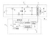
放電灯点灯装置の一例として、図11に示す構成のものがある。この放電灯点灯装置100は、電源回路部101及び点灯制御回路部102で構成されている。電源回路部101は、例えばチョッパ回路であり、直流電源E、負荷109、スイッチング素子Q、スイッチング素子Qに流れる電流を検出する抵抗R、トランスT、ダイオードD、コンデンサC及び負荷109の電圧を検出する負荷電圧検出器103で構成される。電源回路部101のスイッチング素子Qは、点灯制御回路部102のドライブ制御器108から負荷109の状態(電力、電圧等)に応じて出力される駆動信号によってスイッチング動作を行う。
As an example of the discharge lamp lighting device, there is a configuration shown in FIG. The discharge
点灯制御回路部102は、トランスTの2次側から2次電流がゼロになったことを検出するゼロクロス検出器104、スイッチング素子Qに流れる電流と負荷の電力に応じた基準値Isとの大小を比較する電流検出器105、負荷の電力に応じて基準値Isを出力する基準演算部106、負荷電圧検出器103により検出された負荷電圧をA/D変換するA/D変換器107、スイッチング素子Qをオン、オフ制御するドライブ制御器108で構成されている。ドライブ制御器108は例えばRSフリップフロップ等を有して構成されている。
The lighting
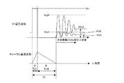
トランスTの電流は、スイッチング素子Qがオンしているオン時間Tonでは、図12(a)に示すように、トランスTにエネルギーを充電し、トランスTの電流は増加する。スイッチング素子Qがオフしているオフ時間Toffでは、図12(b)に示すように、トランスTに蓄えられたエネルギーを放出する回生電流がコンデンサC、ダイオードDを通して流れ、次第に減少する。トランスTに蓄えられているエネルギーをすべて放出すると、トランスTの電流はゼロとなる。 In the on-time Ton when the switching element Q is on, the current of the transformer T charges the transformer T as shown in FIG. 12A, and the current of the transformer T increases. In the off time Toff in which the switching element Q is off, the regenerative current that releases the energy stored in the transformer T flows through the capacitor C and the diode D as shown in FIG. When all the energy stored in the transformer T is released, the current of the transformer T becomes zero.
点灯制御回路部102のゼロクロス検出器104で、トランスTに蓄えられたエネルギーがゼロになったことを検出し、図12(c)に示すように、ドライブ制御器108のセット入力端子SETにスイッチング素子Qのターンオン信号を入力すると、ドライブ制御器108はスイッチング素子Qをターンオンする。負荷電圧検出器103により負荷電圧Vlaを検出し、A/D変換器107を通して基準演算部106でモニターし、負荷の電力に応じた基準値Isを出力する。スイッチング素子Qに流れる電流を抵抗Rで検出した値と、基準値Isの値を電流検出器105で比較し、検出した抵抗Rの電圧値が基準値Isより大きくなれば、図12(d)に示すように、電流検出器105からドライブ制御器108のリセット入力端子RESETに検出信号を入力し、スイッチング素子Qをターンオフする。図12(e)は、ドライブ制御器108の出力端子Doutの電圧出力波形である。これにより、負荷電圧Vlaに応じた適正な電力を供給し、また、トランスTに流れる電流がゼロクロスするタイミングでスイッチング素子Qをターンオン制御することができる。
The zero
特許文献1には、チョッパに流れる電流が所定の基準値以上になるとチョッパをオフし、チョッパコイルのエネルギー放出を検出するとチョッパをオンする放電灯点灯装置において、チョッパのオフ時間を計時するオフ時間タイマー回路を設け、チョッパコイルのエネルギー放出を検出する前にオフ時間タイマー回路により所定時間が計時されると、その計時タイミングでチョッパをオンすることが提案されているが、チョッパコイルのエネルギー放出を検出するゼロクロス検出器を備えるものであった。
放電灯点灯装置において、図11に示すチョッパ回路を用いた電源回路部で、スイッチング素子Qを電流ゼロクロスのタイミングでターンオン制御する場合、トランスTに蓄えられたエネルギーがゼロになったことを検出する動作が必要となるため、トランスTの2次巻線を用いたゼロクロス検出が必要になり、部品点数が多くなり、コストアップを招来するという問題がある。 In the discharge lamp lighting device, when the switching element Q is turned on at the current zero-cross timing in the power supply circuit unit using the chopper circuit shown in FIG. 11, it is detected that the energy stored in the transformer T has become zero. Since the operation is required, zero cross detection using the secondary winding of the transformer T is necessary, and there is a problem that the number of parts increases and the cost increases.
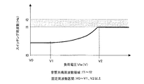
さらには、ゼロクロス検出によりスイッチング素子Qをターンオン制御する場合の動作周波数は、直流電源Eの入力電圧Vin、負荷電圧Vla、負荷電力、トランスTのインダクタンス値により自励で決定されるため、放電灯の負荷電圧Vlaが経時変化すると、スイッチング周波数は図5の破線で示すように変化する。そのスイッチング周波数が負荷電流に重畳し、そのリップル成分が負荷特有の周波数禁止領域に重なる場合、回避することができないという問題もある。 Furthermore, since the operating frequency when the switching element Q is turned on by the zero cross detection is determined by self-excitation based on the input voltage Vin of the DC power source E, the load voltage Vla, the load power, and the inductance value of the transformer T, the discharge lamp When the load voltage Vla changes with time, the switching frequency changes as shown by the broken line in FIG. When the switching frequency is superimposed on the load current and the ripple component is superimposed on a frequency prohibition region specific to the load, there is a problem that it cannot be avoided.
特に、負荷109が高圧放電灯である場合には、負荷特有の周波数禁止領域として音響共鳴現象を生じる領域があり、アークの不安定や立ち消え、ちらつき等を招く恐れがある。
In particular, when the
本発明は上述のような点に鑑みてなされたものであり、放電灯点灯装置のコストアップを招来することなく、放電灯の状態に応じてスイッチング素子の動作周波数を制御し、スイッチング素子のオンタイミングは回生電流がゼロとなったタイミングに制御可能とすることを目的とする。 The present invention has been made in view of the above-described points, and controls the operating frequency of the switching element according to the state of the discharge lamp without increasing the cost of the discharge lamp lighting device. The timing is intended to be controllable at the timing when the regenerative current becomes zero.
請求項1の発明は、上記の課題を解決するために、図1に示すように、放電灯Laに供給する電力を制御するスイッチング回路2を備え、該スイッチング回路2は放電灯Laの状態に応じてスイッチング周波数を制御され、スイッチング素子Qのオン時にインダクタンス要素Lに蓄積されたエネルギーがスイッチング素子Qのオフ時に放出され、そのエネルギー放出電流が略ゼロとなるタイミングでスイッチング素子Qがオン制御される放電灯点灯装置であって、負荷電圧Vlaを検出する負荷電圧検出器5と、前記負荷電圧検出器5から検出された電圧に基づいて所定の放電灯の電力になるようにスイッチング周波数を設定するための時間計測を行うスイッチング周波数計時部8と、前記スイッチング回路2に流れる電流が所定の基準値Isに達したことを検出する電流検出器6と、前記スイッチング周波数計時部8で設定されたスイッチング周波数において前記エネルギー放出電流が略ゼロとなるタイミング以降にスイッチング素子Qがオンされるように前記負荷電圧検出器5から検出された電圧に基づいて前記所定の基準値Isを設定する基準演算部7と、前記スイッチング周波数計時部8の信号を受けてスイッチング素子Qをオン制御、前記電流検出器6の出力信号を受けてスイッチング素子Qをオフ制御するドライブ制御器9とを備え、前記スイッチング周波数計時部8は、図6〜図10に示すように、前記負荷電圧検出器5から検出された電圧に基づいて設定されるスイッチング周波数が動作禁止領域(音響共鳴周波数領域やノイズ発生が問題となる周波数領域)と重なる場合には、スイッチング周波数を動作禁止領域外の固定周波数に設定することを特徴とするものである。
In order to solve the above problems, the invention of
請求項2の発明は、図2に示すように、前記スイッチング回路2の入力電圧Vinを検出する入力電圧検出器12をさらに備え、前記入力電圧検出器12から検出された入力電圧Vinと負荷電圧検出器5から検出された負荷電圧Vlaに基づいて、所定の放電灯の電力になるように前記スイッチング周波数および所定の基準値Isが設定されることを特徴とする。
As shown in FIG. 2, the invention of
請求項3の発明は、請求項1又は2において、前記スイッチング周波数および所定の基準値は、図4に示すように、前記エネルギー放出電流が略ゼロとなった時に発生する自由振動電圧のピーク電圧のタイミングでスイッチング素子Qがオンするように設定されることを特徴とする。 According to a third aspect of the present invention, in the first or second aspect, the switching frequency and the predetermined reference value are, as shown in FIG. 4, the peak voltage of the free oscillation voltage generated when the energy emission current becomes substantially zero. The switching element Q is set to be turned on at the timing.
請求項1の発明によれば、負荷電圧に応じてスイッチング素子のスイッチング周波数を設定し、そのスイッチング周波数となるようにスイッチング周波数計時部でスイッチング素子のオンタイミングを設定し、そのスイッチング周波数においてスイッチング素子のオフ時のエネルギー放出電流が略ゼロとなるタイミングがスイッチング素子の次のオンタイミングとちょうど一致するように、スイッチング素子のオフタイミングを決定する電流の基準値を基準演算部で設定することにより、ゼロクロス検出回路を用いることなく、放電灯の状態に応じてスイッチング素子の動作周波数を制御し、スイッチング素子のオンタイミングは回生電流が略ゼロとなるタイミングに制御することが可能となる。したがって、ゼロクロス検出回路が不要となることで、部品点数を削減し、放電灯点灯装置のコストアップを防止または抑制することができる。また、請求項1の発明によれば、高圧放電灯の音響共鳴が発生する周波数領域やスイッチング回路のノイズ発生が問題となる周波数領域でのスイッチング動作を回避することができる。 According to the first aspect of the present invention, the switching frequency of the switching element is set in accordance with the load voltage, the on-timing of the switching element is set in the switching frequency timer unit so as to be the switching frequency, and the switching element is set at the switching frequency. By setting a reference value of the current that determines the off timing of the switching element in the reference calculation unit so that the timing at which the energy emission current at the time of turning off is substantially zero coincides with the next on timing of the switching element, Without using the zero-cross detection circuit, the operating frequency of the switching element is controlled according to the state of the discharge lamp, and the on-timing of the switching element can be controlled to the timing at which the regenerative current becomes substantially zero. Therefore, since the zero-cross detection circuit is not necessary, the number of parts can be reduced, and the cost increase of the discharge lamp lighting device can be prevented or suppressed. According to the first aspect of the present invention, it is possible to avoid the switching operation in the frequency region where acoustic resonance of the high pressure discharge lamp occurs and in the frequency region where noise generation of the switching circuit becomes a problem.
請求項2の発明によれば、スイッチング回路の入力電圧が異なる場合でも、スイッチング回路の回生電流が略ゼロとなるタイミングでスイッチング素子がオンするように動作させることができる。
According to the invention of
請求項3の発明によれば、スイッチング素子のオフ時電圧が略最小となるタイミングでスイッチング素子がオンするので、スイッチングロスを低減することができる。 According to the third aspect of the present invention, the switching element is turned on at the timing when the off-time voltage of the switching element becomes substantially minimum, so that the switching loss can be reduced.
(実施形態1)
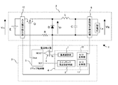
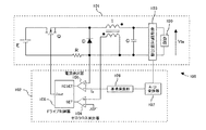
図1は本発明の実施形態1に係る放電灯点灯装置の構成を示す回路図である。図1に示すように、放電灯点灯装置1は、スイッチング回路2とその制御回路3で構成される。スイッチング回路2は、直流電源E、スイッチング素子Q、チョークコイルL、ダイオードD、コンデンサC、抵抗Rを備え、降圧チョッパ回路で構成されている。スイッチング素子Qは、例えばMOSFETからなり、制御回路3から出力される信号によってオン/オフし、負荷の電力を適正に調整するようにスイッチングする。
(Embodiment 1)
FIG. 1 is a circuit diagram showing a configuration of a discharge lamp lighting device according to
制御回路3は、放電灯Laの電力を適正に調整するようにスイッチング素子Qをオン/オフ制御するものであり、電流検出器6、基準演算部7、スイッチング周波数計時部8、ドライブ制御器9、A/D変換器10から構成されている。基準演算部7、スイッチング周波数計時部8、A/D変換器10は、マイクロコンピュータ4内に搭載されている。
The
電流検出器6は、スイッチング素子Qに流れる電流を抵抗Rにより検出した電圧値と、基準演算部7にて放電灯の電力に応じて出力された基準値Isの大小を比較し、スイッチング素子Qのオフ信号を出力する。
The
A/D変換器10は、負荷電圧検出器5で検出された負荷電圧Vla(アナログ値)を所定ビットのデジタル信号に変換するものである。
The A /
基準演算部7は、マイクロコンピュータ4などで構成され、A/D変換後の負荷電圧に基づいて、電流検出器6によりスイッチング素子Qに流れる電流と大小を比較するための基準値Isを出力する。
The
スイッチング周波数計時部8は、マイクロコンピュータ4などで構成され、A/D変換後の負荷電圧に基づいて、ドライブ制御器9にスイッチング素子Qのオン信号を出力し、そのオン信号は、ダイオードDに流れる回生電流がゼロになるタイミングで出力する。 The switching frequency timer 8 includes a microcomputer 4 and the like, and outputs an ON signal of the switching element Q to the drive controller 9 based on the load voltage after A / D conversion, and the ON signal is sent to the diode D. Output when the flowing regenerative current becomes zero.
ドライブ制御器9は、RSフリップフロップなどを用いて構成され、スイッチング周波数計時部8から出力されたターンオン信号をセット入力端子SET側に、電流検出器6から出力されるターンオフ信号をリセット入力端子RESET側に入力することで、図13のように回生電流がゼロになるタイミングでスイッチング素子Qのオン/オフを制御し、放電灯Laの電力を適正に調整する。
The drive controller 9 is configured using an RS flip-flop and the like, and the turn-on signal output from the switching frequency timer 8 is set to the set input terminal SET, and the turn-off signal output from the
基準演算部7の基準値Is、スイッチング周波数計時部8のスイッチング周波数は、直流電源Eからの入力電圧Vin、入力電力Pin、チョッパ回路のチョークコイルLのインダクタンス値L、負荷電圧Vlaがわかれば、以下の式(1)〜(4)より電流ゼロになるスイッチング周期Tcが求められる。
Ip=(Vin−Vla)×Ton/L
=Vla×Toff/L …(1)
Tc=Ton+Toff …(2)
If the reference value Is of the
Ip = (Vin−Vla) × Ton / L
= Vla × Toff / L (1)
Tc = Ton + Toff (2)
上式において、Tonはスイッチング素子Qのオン時間、Toffはスイッチング素子Qのオフ時間、Tcはスイッチング素子Qのスイッチング周期(スイッチング周波数の逆数)であり、単位はsecである。Ipはスイッチング素子Qのピーク電流値(所定の基準値Is=Ip×R)である。また、スイッチング周期Tcが分かれば、(1),(2)式よりスイッチング素子Qのピーク電流Ipを求めることが出来る。チョッパ回路の回生電流がゼロクロスする関係は(1),(2)式で示され、(1),(2)式より、
Pin=Vin×Iin
=Vin×(Vin−Vla)×Ton2 /(2×L×Tc)
=Tc×(Vin−Vla)×Vla2 /(2×L×Vin) …(3)
∴Tc=2×L×Pin×Vin/(Vin−Vla)×Vla2 …(4)
In the above equation, Ton is the ON time of the switching element Q, Toff is the OFF time of the switching element Q, Tc is the switching period of the switching element Q (the reciprocal of the switching frequency), and the unit is sec. Ip is a peak current value of the switching element Q (predetermined reference value Is = Ip × R). If the switching cycle Tc is known, the peak current Ip of the switching element Q can be obtained from the equations (1) and (2). The relationship that the regenerative current of the chopper circuit zero-crosses is shown by the equations (1) and (2). From the equations (1) and (2),
Pin = Vin × Iin
= Vin × (Vin−Vla) × Ton 2 / (2 × L × Tc)
= Tc × (Vin−Vla) × Vla 2 / (2 × L × Vin) (3)
∴Tc = 2 × L × Pin × Vin / (Vin−Vla) × Vla 2 (4)
式(4)より図12に示すTcの時間が求められる。したがって、負荷の電力に応じて回生電流がゼロとなるタイミングでスイッチング素子Qをオン/オフするためには、スイッチング周期Tc、基準値Isは、負荷電圧Vlaに応じて可変する必要がある。 The time Tc shown in FIG. 12 is obtained from the equation (4). Therefore, in order to turn on / off the switching element Q at the timing when the regenerative current becomes zero according to the power of the load, the switching cycle Tc and the reference value Is need to be varied according to the load voltage Vla.
本実施形態では、スイッチング周期Tc、基準値Isの出力機能をマイクロコンピュータ4に集約し、A/D変換器10で負荷電圧Vlaを監視しながら、所定の放電灯の電力になるように、スイッチング周期Tcと基準値Isを負荷電圧Vlaに応じて可変制御することで、ゼロクロス検出回路を用いる必要がなくなり、部品点数を削減し、放電灯点灯装置のコストアップを防止または抑制することができる。
In the present embodiment, the switching function Tc and the output function of the reference value Is are integrated into the microcomputer 4 and the load voltage Vla is monitored by the A /
マイクロコンピュータ4の演算速度については、A/D変換器10で負荷電圧Vlaを読み込むたびに前記演算式を用いて演算し、出力する構成にすると、高速度のマイクロコンピュータ4が必要となり、部品コストが高価となる。そこで、マイクロコンピュータ4には、あらかじめ負荷電圧Vlaに対する基準値Is、スイッチング周期Tcのテーブルデータをメモリ上に保持しておく。負荷電圧Vlaの読み込みのタイミングは、放電灯Laの負荷電圧Vlaが比較的ゆっくりと変化するものにおいては、例えば負荷電圧Vlaを1msec〜5msec間隔で読み込んで、次の負荷電圧Vlaを読み込むまでは、基準値Is、スイッチング周期Tcは更新しない制御にする。このように、予め用意してあるテーブルデータから基準値Is、スイッチング周期Tcを出力することで、比較的安価なマイクロコンピュータ4を用いて構成することができる。
The calculation speed of the microcomputer 4 is calculated by using the above-described calculation formula every time the load voltage Vla is read by the A /
このように、チョッパ回路のダイオードDに流れる回生電流がゼロになるタイミングでスイッチング素子Qをターンオン制御するためのデータを予めマイクロコンピュータ4のメモリ上にテーブルデータとして用意しておいて、スイッチング素子Qのオン/オフタイミングの制御機能をマイクロコンピュータ4に集約することで、従来のようなトランスTの2次巻線を用いたゼロクロス検出が不要となり、コストアップを防止または抑制することができる。 In this way, data for turning on the switching element Q at the timing when the regenerative current flowing through the diode D of the chopper circuit becomes zero is prepared as table data in the memory of the microcomputer 4 in advance. By integrating the control function of the on / off timing in the microcomputer 4, zero cross detection using the secondary winding of the transformer T as in the prior art becomes unnecessary, and cost increase can be prevented or suppressed.
(実施形態2)
図2は本発明の実施形態2に係る放電灯点灯装置の構成を示す回路図である。図2の回路は、上述の図1の回路において、直流電源Eからの入力電圧Vinを監視する入力電圧検出器12と、入力電圧検出器12で検出された入力電圧(アナログ値)を所定ビットのデジタル値に変換するA/D変換器11を追加したものである。
(Embodiment 2)
FIG. 2 is a circuit diagram showing a configuration of a discharge lamp lighting device according to
直流電源Eからの入力電圧Vinが変われば、上述の演算式における基準値Is、スイッチング周期Tcは変化する。よって、マイクロコンピュータ4内には、直流電源Eからの入力電圧Vinの違いに応じて、負荷電圧Vlaに対する基準値Is、スイッチング周期Tcのテーブルデータを複数保持しておく。直流電源Eが投入されたとき、入力電圧検出器12により検出された入力電圧をマイクロコンピュータ4のA/D変換器11でデジタル値として取り込み、その入力電圧に応じた基準値Is、スイッチング周期Tcのテーブルデータを選択して制御する。これにより、直流電源Eの電圧変化に対しても放電灯Vlaの電力に応じて回生電流がゼロになるタイミングでスイッチング素子Qをターンオンさせるように制御することができる。
If the input voltage Vin from the DC power source E changes, the reference value Is and the switching period Tc in the above-described arithmetic expression change. Therefore, a plurality of table data of the reference value Is and the switching period Tc for the load voltage Vla are held in the microcomputer 4 according to the difference in the input voltage Vin from the DC power supply E. When the DC power source E is turned on, the input voltage detected by the
図1又は図2において、スイッチング回路2は降圧チョッパ回路の構成である場合について説明したが、入力電圧変動幅など設計条件によっては、降圧チョッパ回路でなく、昇圧チョッパ回路や昇降圧チョッパ回路を用いる場合もある。そのような場合にも、本発明を適用できることは言うまでもない。
1 or 2, the switching
(実施形態3)
図1又は図2に示す回路構成において、ダイオードDに流れる回生電流がゼロになった後にスイッチング素子Qがオンしなければ、ダイオードDの電圧Vrは、図3のように自由振動しながら負荷電圧Vlaに収束する。自由振動電圧のピーク高さは、負荷電圧Vlaの値により変動する。図3に示すように、Vla1<Vla2であれば、Vrp1<Vrp2となる。また、自由振動の周期は、チョッパ回路のスイッチング素子Q、ダイオードDの寄生容量で決定され、ほぼ固定値なので、負荷電圧Vlaが変化しても自由振動電圧の周期は変わらない。
(Embodiment 3)
In the circuit configuration shown in FIG. 1 or FIG. 2, if the switching element Q does not turn on after the regenerative current flowing through the diode D becomes zero, the voltage Vr of the diode D is the load voltage while freely oscillating as shown in FIG. It converges to Vla. The peak height of the free vibration voltage varies depending on the value of the load voltage Vla. As shown in FIG. 3, if Vla1 <Vla2, Vrp1 <Vrp2. The period of the free vibration is determined by the parasitic capacitance of the switching element Q and the diode D of the chopper circuit, and is almost a fixed value. Therefore, the period of the free vibration voltage does not change even when the load voltage Vla changes.
そこで、図4に示すようにダイオードDに流れる回生電流がゼロになった時間から、自由振動電圧の1回目の半波のピーク電圧Vrpになる時間Tdを所定時間とし、上述のスイッチング周期Tcに所定時間Tdを足した時間で、スイッチング素子Qをオンするようにスイッチング周期(Tc+Td)を設定すれば、スイッチング素子Qに印加される電圧は、直流電源Eの入力電圧Vinから自由振動電圧のピーク電圧Vrpを差し引いた値となり、スイッチング素子Qのスイッチングロスが低減される。また、負荷電圧Vlaが変化しても、自由振動電圧の1回目の半波のピーク電圧Vrpになる時間Tdを所定時間として設定しているので、常に自由振動電圧のピーク電圧Vrpのタイミングでスイッチング素子Qがターンオンするように制御できる。 Therefore, as shown in FIG. 4, from the time when the regenerative current flowing through the diode D becomes zero, the time Td at which the first half-wave peak voltage Vrp of the free oscillation voltage becomes the predetermined time is defined as a predetermined time, and the switching cycle Tc described above is reached. If the switching period (Tc + Td) is set so that the switching element Q is turned on by the time obtained by adding the predetermined time Td, the voltage applied to the switching element Q is the peak of the free vibration voltage from the input voltage Vin of the DC power supply E. The voltage Vrp is subtracted, and the switching loss of the switching element Q is reduced. Even when the load voltage Vla changes, the time Td during which the first half-wave peak voltage Vrp of the free vibration voltage becomes the predetermined time is set as the predetermined time, so that switching is always performed at the timing of the peak voltage Vrp of the free vibration voltage. The device Q can be controlled to turn on.
(実施形態4)
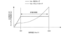
図1又は図2に示す回路構成において、負荷である放電灯LaがHIDランプ(高輝度高圧放電灯)の場合、図5に示すように、負荷電圧Vlaが定格電圧範囲(例えば50〜150V)において定電力制御を求められる。図中、実線は負荷電圧Vlaと出力電力の関係を示しており、破線は負荷電圧Vlaとチョッパのスイッチング周波数の関係を示している。図5の実線で示すように、負荷電圧Vlaの上昇に対して出力電力が一定となるように制御しようとすると、チョッパ電流がゼロになったタイミングでスイッチング素子Qをオンさせる場合には、図5の破線で示すように、負荷電圧Vlaが大きくなるにつれて、スイッチング周波数は高くなる。スイッチング周波数が変化する範囲内に、HIDランプに特有の音響共鳴周波数領域が存在する場合、スイッチング素子Qのスイッチング周波数が音響共鳴周波数領域を通過するとき、負荷電流に重畳するスイッチング周波数のリップル成分によりHIDランプのちらつきを発生させることがある。
(Embodiment 4)
In the circuit configuration shown in FIG. 1 or FIG. 2, when the discharge lamp La as a load is an HID lamp (high-intensity high-pressure discharge lamp), the load voltage Vla is within a rated voltage range (for example, 50 to 150 V) as shown in FIG. Constant power control is required. In the figure, the solid line shows the relationship between the load voltage Vla and the output power, and the broken line shows the relationship between the load voltage Vla and the switching frequency of the chopper. As shown by the solid line in FIG. 5, when the switching element Q is turned on at the timing when the chopper current becomes zero when the output power is controlled to be constant with respect to the increase of the load voltage Vla, As indicated by the
そこで、図6に示すように、HIDランプの音響共鳴周波数領域がf1〜f2、f3〜f4に存在する場合、その音響共鳴周波数領域にかかる負荷電圧V1〜V2、V3〜V4の区間のスイッチング周波数を音響共鳴周波数領域にかかる手前の周波数で固定周波数にし、その固定周波数で負荷の電力に応じた基準値Isを設定し、スイッチング素子Qを制御する。 Therefore, as shown in FIG. 6, when the acoustic resonance frequency region of the HID lamp exists in f1 to f2 and f3 to f4, the switching frequency in the section of the load voltages V1 to V2 and V3 to V4 applied to the acoustic resonance frequency region. Is set to a fixed frequency at a frequency in front of the acoustic resonance frequency region, a reference value Is corresponding to the power of the load is set at the fixed frequency, and the switching element Q is controlled.
本実施形態によれば、マイクロコンピュータ4に設定してある負荷電圧Vlaに応じたスイッチング周期Tc、基準値Isのテーブルデータを変更するだけで、音響共鳴周波数を避ける切り替え回路などを必要としないので、コストアップを招来することなく、容易に音響共鳴周波数での動作を回避することができる。また、音響共鳴周波数領域が違う放電灯においてもテーブルデータを変更するだけで容易に対応することができる。 According to the present embodiment, since only the table data of the switching period Tc and the reference value Is corresponding to the load voltage Vla set in the microcomputer 4 is changed, a switching circuit for avoiding the acoustic resonance frequency is not required. The operation at the acoustic resonance frequency can be easily avoided without incurring an increase in cost. Moreover, it is possible to easily cope with a discharge lamp having a different acoustic resonance frequency region by simply changing the table data.
(実施形態5)
図7は本発明の実施形態5の動作説明図である。回路構成は図1又は図2と同様である。本実施形態では、上述の実施形態4と同様に、HIDランプの音響共鳴周波数領域がf1〜f2、f3〜f4に存在する場合、その音響共鳴周波数領域にかかる負荷電圧V1〜V2、V3〜V4の区間のスイッチング周波数を音響共鳴周波数領域にかかる手前の周波数で固定周波数にすることで、音響共鳴周波数での動作を回避すると共に、負荷電圧Vlaが高いV5以上の領域では、固定周波数にするものである。これは、負荷電圧Vlaが高いV5以上の領域では、負荷電圧Vlaが上がるにつれてスイッチング周波数が高い領域になるため、固定周波数にすることで、チョッパ回路としてスイッチングノイズを低減するものである。
(Embodiment 5)
FIG. 7 is an operation explanatory diagram of
(実施形態6)
図8は本発明の実施形態6の動作説明図である。回路構成は図1又は図2と同様である。本実施形態では、上述の実施形態4と同様に、HIDランプの音響共鳴周波数領域がf1〜f2、f3〜f4に存在する場合、その音響共鳴周波数領域にかかる負荷電圧V2〜V3、V4〜V5の区間のスイッチング周波数を音響共鳴周波数領域にかかる手前の周波数で固定周波数にすることで、音響共鳴周波数での動作を回避すると共に、負荷電圧Vlaが低いV1以下の領域では、固定周波数にするものである。これは、負荷電圧Vlaが低い領域まで出力電力の低下に応じてスイッチング周波数を低下させると、スイッチング周波数が可聴領域に入る可能性があるため、負荷電圧VlaがV1以下の領域ではスイッチング周波数を固定周波数とすることで、可聴ノイズの発生を回避するものである。
(Embodiment 6)
FIG. 8 is an operation explanatory diagram of
(実施形態7)
図9は本発明の実施形態7の動作説明図である。回路構成は図1又は図2と同様である。本実施形態では、HIDランプの音響共鳴周波数領域がf1〜f2に存在する場合、その音響共鳴周波数領域にかかる負荷電圧V2以上の区間のスイッチング周波数を音響共鳴周波数領域にかかる手前の周波数f1で固定周波数にすることで、音響共鳴周波数での動作を回避するものである。また、負荷電圧Vlaが低いV1以下の領域では、固定周波数にするものである。すなわち、音響共鳴周波数f1以上では、スイッチング周波数を固定周波数として音響共鳴周波数f1以上の領域を全て回避し、また、負荷電圧Vlaが低い領域ではスイッチング周波数が可聴領域に入る可能性があるため、負荷電圧V1以下は全て固定周波数とすることで、可聴ノイズの発生も回避するものである。
(Embodiment 7)
FIG. 9 is an operation explanatory diagram of
(実施形態8)
図10は本発明の実施形態8の動作説明図である。回路構成は図1又は図2と同様である。本実施形態は、図7に示した実施形態5と図8に示した実施形態6の組み合わせであり、HIDランプの音響共鳴周波数領域がf1〜f2、f3〜f4に存在する場合、その音響共鳴周波数領域にかかる負荷電圧V2〜V3、V4〜V5の区間のスイッチング周波数を音響共鳴周波数領域にかかる手前の周波数で固定周波数にすることで、音響共鳴周波数での動作を回避すると共に、負荷電圧Vlaが高いV6以上の領域では、固定周波数にするものである。また、負荷電圧Vlaが低いV1以下の領域では、固定周波数にするものである。本実施形態の作用効果は実施形態5,6の作用効果を合わせたものであり、負荷電圧Vlaが高いV6以上の領域では、固定周波数にすることで、スイッチング周波数が高くなり過ぎることを回避し、チョッパ回路としてスイッチングノイズを低減するものである。また、負荷電圧VlaがV1以下の領域ではスイッチング周波数を固定周波数とすることで、スイッチング周波数が可聴領域に入ることを回避し、可聴ノイズの発生も回避するものである。
(Embodiment 8)
FIG. 10 is an operation explanatory diagram of Embodiment 8 of the present invention. The circuit configuration is the same as in FIG. 1 or FIG. This embodiment is a combination of the
(実施形態9)
上述の各実施形態1〜8の放電灯点灯装置は、プロジェクタやリアプロジェクションテレビのような画像表示装置の光源となる放電灯の点灯に用いられる。ここでは、プロジェクタに実装する場合を例示する。図14は画像表示装置30の内部構成を示す概略構成図である。図中、31は投光窓、32は電源部、33a,33b,33cは冷却用ファン、34は外部信号入力部、35は光学系、36はメイン制御基板、40は放電灯点灯装置、Laは放電灯である。破線で示した枠内にメイン制御基板36が実装されている。光学系35の途中には、放電灯Laからの光を透過または反射する画像表示手段(透過型液晶表示板または反射型画像表示素子)が設けられており、この画像表示手段を介する透過光または反射光をスクリーンに投射するように光学系35が設計されている。このように、放電灯点灯装置40は放電灯Laと共に画像表示装置30の内部に実装されているが、本発明の放電灯点灯装置40を採用することにより、従来よりも部品点数が少なく安価に構成することができる。また、スイッチングロスを低減できるから、冷却用ファンの静音化が可能となる。さらに、高圧放電灯に特有の音響共鳴周波数での動作を回避し、ちらつきを防止できる。
(Embodiment 9)
The above-described discharge lamp lighting devices according to the first to eighth embodiments are used for lighting a discharge lamp serving as a light source of an image display device such as a projector or a rear projection television. Here, the case where it mounts in a projector is illustrated. FIG. 14 is a schematic configuration diagram showing the internal configuration of the
1 放電灯点灯装置
2 スイッチング回路
3 制御回路
4 マイクロコンピュータ
5 負荷電圧検出器
6 電流検出器
7 基準演算部
8 スイッチング周波数計時部
9 ドライブ制御器
10 A/D変換器
11 A/D変換器
12 入力電圧検出器
La 放電灯
DESCRIPTION OF
Claims (4)
負荷電圧を検出する負荷電圧検出器と、
前記負荷電圧検出器から検出された電圧に基づいて所定の放電灯の電力になるようにスイッチング周波数を設定するための時間計測を行うスイッチング周波数計時部と、
前記スイッチング回路に流れる電流が所定の基準値に達したことを検出する電流検出器と、
前記スイッチング周波数計時部で設定されたスイッチング周波数において前記エネルギー放出電流が略ゼロとなるタイミング以降にスイッチング素子がオンされるように前記負荷電圧検出器から検出された電圧に基づいて前記所定の基準値を設定する基準演算部と、
前記スイッチング周波数計時部の信号を受けてスイッチング素子をオン制御、前記電流検出器の出力信号を受けてスイッチング素子をオフ制御するドライブ制御器とを備え、
前記スイッチング周波数計時部は、前記負荷電圧検出器から検出された電圧に基づいて設定されるスイッチング周波数が動作禁止領域と重なる場合には、スイッチング周波数を動作禁止領域外の固定周波数に設定することを特徴とする放電灯点灯装置。 A switching circuit for controlling the power supplied to the discharge lamp is provided. The switching circuit controls the switching frequency according to the state of the discharge lamp, and the energy stored in the inductance element when the switching element is turned on is released when the switching element is turned off. A discharge lamp lighting device in which the switching element is on-controlled at a timing when the energy emission current becomes substantially zero,
A load voltage detector for detecting the load voltage;
A switching frequency timer that performs time measurement for setting the switching frequency so as to be the power of a predetermined discharge lamp based on the voltage detected from the load voltage detector;
A current detector for detecting that the current flowing through the switching circuit has reached a predetermined reference value;
The predetermined reference value based on the voltage detected from the load voltage detector so that the switching element is turned on after the timing when the energy emission current becomes substantially zero at the switching frequency set by the switching frequency timer. A reference calculation unit for setting
A switching controller that receives a signal from the switching frequency timer and that controls the switching element; and a drive controller that receives the output signal of the current detector and controls the switching element to turn off ;
When the switching frequency set based on the voltage detected from the load voltage detector overlaps the operation prohibition region, the switching frequency timer unit sets the switching frequency to a fixed frequency outside the operation prohibition region. A discharge lamp lighting device characterized.
Priority Applications (5)
| Application Number | Priority Date | Filing Date | Title |
|---|---|---|---|
| JP2005368957A JP4735239B2 (en) | 2005-12-22 | 2005-12-22 | Discharge lamp lighting device and image display device |
| CN2006800482135A CN101341801B (en) | 2005-12-22 | 2006-12-21 | Discharge lamp lighting device and image display device |
| PCT/JP2006/325546 WO2007072925A1 (en) | 2005-12-22 | 2006-12-21 | Discharge lamp lighting device and image display device |
| US12/096,088 US7943890B2 (en) | 2005-12-22 | 2006-12-21 | Discharge lamp lighting device and image display device with switching frequency |
| EP06843020A EP1965612B1 (en) | 2005-12-22 | 2006-12-21 | Discharge lamp lighting device and image display device |
Applications Claiming Priority (1)
| Application Number | Priority Date | Filing Date | Title |
|---|---|---|---|
| JP2005368957A JP4735239B2 (en) | 2005-12-22 | 2005-12-22 | Discharge lamp lighting device and image display device |
Publications (2)
| Publication Number | Publication Date |
|---|---|
| JP2007173024A JP2007173024A (en) | 2007-07-05 |
| JP4735239B2 true JP4735239B2 (en) | 2011-07-27 |
Family
ID=38188700
Family Applications (1)
| Application Number | Title | Priority Date | Filing Date |
|---|---|---|---|
| JP2005368957A Expired - Fee Related JP4735239B2 (en) | 2005-12-22 | 2005-12-22 | Discharge lamp lighting device and image display device |
Country Status (5)
| Country | Link |
|---|---|
| US (1) | US7943890B2 (en) |
| EP (1) | EP1965612B1 (en) |
| JP (1) | JP4735239B2 (en) |
| CN (1) | CN101341801B (en) |
| WO (1) | WO2007072925A1 (en) |
Families Citing this family (9)
| Publication number | Priority date | Publication date | Assignee | Title |
|---|---|---|---|---|
| JP4807454B2 (en) * | 2007-06-20 | 2011-11-02 | パナソニック電工株式会社 | Discharge lamp lighting device, lighting device, and liquid crystal display device |
| WO2009011092A1 (en) * | 2007-07-19 | 2009-01-22 | Panasonic Corporation | Image display device |
| JP2009032471A (en) * | 2007-07-26 | 2009-02-12 | Panasonic Electric Works Co Ltd | Discharge lamp lighting device and lighting fixture |
| JP5015866B2 (en) * | 2008-06-18 | 2012-08-29 | 本田技研工業株式会社 | DC / DC converter device, power system, fuel cell vehicle, and physical value input method for controller of DC / DC converter device |
| JP5267117B2 (en) * | 2008-12-26 | 2013-08-21 | セイコーエプソン株式会社 | Discharge lamp lighting device, projector, and control method of discharge lamp lighting device |
| JP5884046B2 (en) * | 2011-10-24 | 2016-03-15 | パナソニックIpマネジメント株式会社 | Lighting device and lighting apparatus using the same |
| JP6065194B2 (en) * | 2012-04-13 | 2017-01-25 | パナソニックIpマネジメント株式会社 | Discharge lamp lighting device, in-vehicle illumination device including the same, and vehicle |
| CN103945593B (en) * | 2013-01-22 | 2016-08-03 | 上海鸣志自动控制设备有限公司 | A kind of LED drives hot plug control circuit |
| WO2018235199A1 (en) * | 2017-06-21 | 2018-12-27 | 三菱電機株式会社 | Light source lighting device, lighting equipment |
Family Cites Families (21)
| Publication number | Priority date | Publication date | Assignee | Title |
|---|---|---|---|---|
| JPH05176526A (en) | 1991-12-24 | 1993-07-13 | Matsushita Electric Works Ltd | Power supply device |
| JP3470529B2 (en) * | 1996-11-15 | 2003-11-25 | 松下電工株式会社 | Discharge lamp lighting device |
| US5859505A (en) | 1997-10-02 | 1999-01-12 | Philips Electronics North America Corporation | Method and controller for operating a high pressure gas discharge lamp at high frequencies to avoid arc instabilities |
| US6043633A (en) * | 1998-06-05 | 2000-03-28 | Systel Development & Industries | Power factor correction method and apparatus |
| JP3829534B2 (en) * | 1999-05-26 | 2006-10-04 | 松下電工株式会社 | Discharge lamp lighting device |
| US6693393B2 (en) * | 2001-01-12 | 2004-02-17 | Matsushita Electric Works, Ltd. | Ballast for a discharge lamp |
| WO2002056646A2 (en) * | 2001-01-12 | 2002-07-18 | Matsushita Electric Works, Ltd. | Ballast for a discharge lamp |
| JP2003100485A (en) * | 2001-09-20 | 2003-04-04 | Hitachi Media Electoronics Co Ltd | Discharge lamp lighting circuit |
| JP3736438B2 (en) * | 2001-11-26 | 2006-01-18 | ウシオ電機株式会社 | Light source device and power supply device |
| EP1558064B1 (en) * | 2002-10-28 | 2014-07-09 | Panasonic Corporation | High-pressure discharge lamp operation device and illumination appliance having the same |
| JP4306233B2 (en) | 2002-11-26 | 2009-07-29 | パナソニック電工株式会社 | Discharge lamp lighting device |
| JP4241027B2 (en) | 2002-12-24 | 2009-03-18 | パナソニック電工株式会社 | Power supply |
| JP4247048B2 (en) * | 2003-06-05 | 2009-04-02 | 株式会社小糸製作所 | DC voltage converter |
| JP4534438B2 (en) * | 2003-06-30 | 2010-09-01 | パナソニック電工株式会社 | Discharge lamp lighting device |
| JP4178465B2 (en) | 2003-08-27 | 2008-11-12 | 三菱電機株式会社 | High pressure discharge lamp lighting device and lighting fixture |
| JP2005184964A (en) | 2003-12-18 | 2005-07-07 | Renesas Technology Corp | Power unit and its control method |
| JP4561097B2 (en) * | 2003-12-26 | 2010-10-13 | パナソニック電工株式会社 | Discharge lamp lighting device and lighting device |
| JP2005312105A (en) | 2004-04-16 | 2005-11-04 | Matsushita Electric Ind Co Ltd | Buck converter |
| JP4241515B2 (en) * | 2004-06-10 | 2009-03-18 | パナソニック電工株式会社 | Discharge lamp lighting device and projector |
| JP4665480B2 (en) * | 2004-10-26 | 2011-04-06 | パナソニック電工株式会社 | Discharge lamp lighting device, lighting fixture, and lighting system |
| US7365951B2 (en) * | 2006-03-07 | 2008-04-29 | Matsushita Electric Works, Ltd. | Discharge lamp lighting device, lighting system and method |
-
2005
- 2005-12-22 JP JP2005368957A patent/JP4735239B2/en not_active Expired - Fee Related
-
2006
- 2006-12-21 US US12/096,088 patent/US7943890B2/en not_active Expired - Fee Related
- 2006-12-21 CN CN2006800482135A patent/CN101341801B/en not_active Expired - Fee Related
- 2006-12-21 WO PCT/JP2006/325546 patent/WO2007072925A1/en not_active Ceased
- 2006-12-21 EP EP06843020A patent/EP1965612B1/en not_active Ceased
Also Published As
| Publication number | Publication date |
|---|---|
| WO2007072925A1 (en) | 2007-06-28 |
| CN101341801B (en) | 2012-07-04 |
| EP1965612A4 (en) | 2011-07-27 |
| CN101341801A (en) | 2009-01-07 |
| US20090323033A1 (en) | 2009-12-31 |
| US7943890B2 (en) | 2011-05-17 |
| JP2007173024A (en) | 2007-07-05 |
| EP1965612B1 (en) | 2013-01-23 |
| EP1965612A1 (en) | 2008-09-03 |
Similar Documents
| Publication | Publication Date | Title |
|---|---|---|
| JP4665480B2 (en) | Discharge lamp lighting device, lighting fixture, and lighting system | |
| JP4735239B2 (en) | Discharge lamp lighting device and image display device | |
| WO2005122652A1 (en) | Discharge lamp lighting device and projector | |
| JP2009200146A (en) | Led drive circuit and led illumination apparatus using it | |
| JP4168660B2 (en) | Discharge lamp lighting device | |
| JP2006024511A (en) | Discharge lamp lighting device | |
| US8941321B2 (en) | Discharge lamp lighting device, and illumination apparatus and vehicle including same | |
| JP5077593B2 (en) | Discharge lamp lighting device, projector, and control method of discharge lamp lighting device | |
| JP4480073B2 (en) | Discharge lamp lighting device | |
| JP2009272255A (en) | Discharge lamp lighting device, lighting device | |
| JP4775003B2 (en) | Discharge lamp lighting device and image display device | |
| JP4710591B2 (en) | Discharge lamp lighting device and image display device | |
| JP4678425B2 (en) | Discharge lamp lighting device | |
| JP4793122B2 (en) | Discharge lamp lighting device and image display device | |
| JP4862392B2 (en) | High pressure discharge lamp lighting device and image display device | |
| JP4802906B2 (en) | Discharge lamp lighting device and projector | |
| JP4710590B2 (en) | Discharge lamp lighting device and image display device | |
| JP5537118B2 (en) | High pressure discharge lamp lighting device and image display device using the same | |
| JP5032869B2 (en) | Discharge lamp lighting device | |
| JP2011097680A (en) | Power supply device, lighting device, and lighting fixture | |
| JP5102446B2 (en) | Discharge lamp lighting device and image display device | |
| JPH09232094A (en) | Discharge lamp lighting device | |
| JPH0574579A (en) | Incandescent lamp lighting device | |
| JP2007311088A (en) | Discharge lamp lighting device | |
| JP2008220075A (en) | Cooling fan drive voltage control device, cooling device and projector |
Legal Events
| Date | Code | Title | Description |
|---|---|---|---|
| A621 | Written request for application examination |
Free format text: JAPANESE INTERMEDIATE CODE: A621 Effective date: 20080825 |
|
| A131 | Notification of reasons for refusal |
Free format text: JAPANESE INTERMEDIATE CODE: A131 Effective date: 20101221 |
|
| A521 | Request for written amendment filed |
Free format text: JAPANESE INTERMEDIATE CODE: A523 Effective date: 20110218 |
|
| TRDD | Decision of grant or rejection written | ||
| A01 | Written decision to grant a patent or to grant a registration (utility model) |
Free format text: JAPANESE INTERMEDIATE CODE: A01 Effective date: 20110329 |
|
| A61 | First payment of annual fees (during grant procedure) |
Free format text: JAPANESE INTERMEDIATE CODE: A61 Effective date: 20110411 |
|
| R150 | Certificate of patent or registration of utility model |
Ref document number: 4735239 Country of ref document: JP Free format text: JAPANESE INTERMEDIATE CODE: R150 Free format text: JAPANESE INTERMEDIATE CODE: R150 |
|
| FPAY | Renewal fee payment (event date is renewal date of database) |
Free format text: PAYMENT UNTIL: 20140513 Year of fee payment: 3 |
|
| LAPS | Cancellation because of no payment of annual fees |