JP4802906B2 - Discharge lamp lighting device and projector - Google Patents
Discharge lamp lighting device and projector Download PDFInfo
- Publication number
- JP4802906B2 JP4802906B2 JP2006201351A JP2006201351A JP4802906B2 JP 4802906 B2 JP4802906 B2 JP 4802906B2 JP 2006201351 A JP2006201351 A JP 2006201351A JP 2006201351 A JP2006201351 A JP 2006201351A JP 4802906 B2 JP4802906 B2 JP 4802906B2
- Authority
- JP
- Japan
- Prior art keywords
- discharge lamp
- output
- period
- switching element
- lighting device
- Prior art date
- Legal status (The legal status is an assumption and is not a legal conclusion. Google has not performed a legal analysis and makes no representation as to the accuracy of the status listed.)
- Expired - Fee Related
Links
Images


Landscapes
- Circuit Arrangements For Discharge Lamps (AREA)
- Dc-Dc Converters (AREA)
Description
本発明は、例えば、水銀ランプ、メタルハライドランプ等の高圧放電灯を点灯させるのに適した放電灯点灯装置、及びそれを用いたプロジェクタに関するものである。 The present invention relates to a discharge lamp lighting device suitable for lighting a high pressure discharge lamp such as a mercury lamp and a metal halide lamp, and a projector using the same.
図10は従来のスイッチング回路の制御系を示すブロック図である。スイッチング回路10から負荷11への出力を検出した検出値1をマイコン12などの演算回路に入力し、制御目標となる出力を決定する。マイコン12の出力をD/A変換回路13に入力し、そのD/A変換回路13の出力値とスイッチング回路10より検出した検出値2を比較回路14にて比較し、その結果をドライブ回路15に伝達してスイッチング回路10のスイッチング動作を決定する。マイコン12の出力はデジタル出力であり、D/A変換回路13によりデジタル出力をアナログ出力に変換している。D/A変換回路13には例えば図11のような抵抗ラダー回路などが用いられる。図示された例では、マイコン12は8ビットのデジタル値を出力しており、抵抗Ra〜Rqの分圧回路によりアナログ電圧Vxに変換して出力される。
FIG. 10 is a block diagram showing a control system of a conventional switching circuit. The detection value 1 detected from the output from the
図12にD/A変換回路の入出力の関係を示す。マイコンのデジタル出力より得られるD/A変換回路の出力はマイコンのデジタル出力に応じて階段状に変化し、理想の出力線との誤差が発生する。その誤差がスイッチング回路の出力の誤差を生じさせる。放電灯点灯装置ではスイッチング回路の出力の誤差は負荷である放電灯の光の誤差となる。また、D/A変換回路の出力の階段状の段上がり部分では光の変動が急激になるため、光がちらついて見える要因ともなる。この誤差を低減する従来の手段としては、マイコンからの出力ポート数を増やして階段状の出力を細分化する手段などがある。 FIG. 12 shows the input / output relationship of the D / A conversion circuit. The output of the D / A conversion circuit obtained from the digital output of the microcomputer changes stepwise according to the digital output of the microcomputer, and an error from the ideal output line occurs. The error causes an error in the output of the switching circuit. In the discharge lamp lighting device, an error in the output of the switching circuit becomes an error in the light of the discharge lamp as a load. In addition, since the fluctuation of the light becomes abrupt at the stepped stepped portion of the output of the D / A conversion circuit, it becomes a factor that the light appears to flicker. As a conventional means for reducing this error, there is a means for increasing the number of output ports from the microcomputer and subdividing the stepped output.
特許文献1にはマイコンなどのデジタル演算回路の出力をD/A変換して得た制御電圧により放電灯の光出力を制御する放電灯点灯装置において、制御電圧の分解能を向上させる技術が開示されている。これは放電灯の光出力が小さくなる低出力時において、最大値付近となるように整数倍した大きなデジタル値を出力し、D/A変換した後の制御電圧を整数分の1に減衰させることで低出力時の制御電圧の分解能を高める技術である。
特許文献1の手段では、低出力時には制御電圧の分解能を高めることが出来るが、高出力時には制御電圧の分解能を高めることはできない。また、マイコンからの出力ポート数を増やして階段状の出力を細分化するような手段では、マイコンの大型化やコストアップ、またマイコンに付帯する抵抗などの回路部品数の増加による回路装置の大型化やコストアップになってしまう。 With the means of Patent Document 1, the resolution of the control voltage can be increased at the time of low output, but the resolution of the control voltage cannot be increased at the time of high output. In addition, with the means to increase the number of output ports from the microcomputer and subdivide the staircase output, the size and cost of the microcomputer will increase, and the size of the circuit device will increase due to the increase in the number of circuit components such as resistors attached to the microcomputer. Will increase the cost and cost.
本発明は上述の点に鑑みてなされたものであり、D/A変換回路の出力によりスイッチング素子のオン期間を制御されるスイッチング回路の出力の誤差を少なくして出力精度を上げ、また安定した出力を得られる、小型で安価な放電灯点灯装置を提供することを課題とする。 The present invention has been made in view of the above-described points, and the output accuracy of the switching circuit, in which the ON period of the switching element is controlled by the output of the D / A conversion circuit, is reduced, and the output accuracy is improved. It is an object to provide a small and inexpensive discharge lamp lighting device capable of obtaining an output.
請求項1の発明は、上記の課題を解決するために、図1に示すように、デジタル出力をD/A変換回路13へ入力し、そのD/A変換回路13の出力をもってスイッチング素子Q1のオン期間とし、図2に示すように、スイッチング素子Q1の動作周期Tをあらかじめ定めることでスイッチング素子Q1のオフ期間を定めるスイッチング回路にて放電灯Laへ電力を供給する放電灯点灯装置において、少なくともデジタル出力が一定である期間中にスイッチング素子Q1の動作周期Tを変化させるようにしたことを特徴とする。
In order to solve the above problem, the invention of claim 1 inputs a digital output to a D /
請求項2の発明は、上記の課題を解決するために、図1に示すように、放電灯Laの点灯状態の電気量を検出する検出回路と、検出回路の検出値が所定の範囲内では一定のデジタル値を出力するマイコン12を含む演算回路と、マイコン12からのデジタル出力をD/A変換するD/A変換回路13と、D/A変換回路13の出力に応じたオン期間でスイッチングするスイッチング素子Q1を備え、あらかじめ定めたスイッチング素子Q1の動作周期Tに対するオン期間の割合で放電灯Laへの電力を制御する放電灯点灯装置において、少なくともデジタル出力が一定である期間中に上記検出値の変化に応じた放電灯Laの電力の変化を抑制する方向にスイッチング素子Q1の動作周期Tを変化させることを特徴とする。
In order to solve the above-described problem, the invention of claim 2 detects a quantity of electricity in the lighting state of the discharge lamp La and a detection value of the detection circuit within a predetermined range as shown in FIG. An arithmetic circuit including a
請求項3の発明は、請求項2において、放電灯Laの点灯状態の電気量はランプ電圧値あるいはこれに相当する値であって、少なくともデジタル出力が一定である期間中に上記電気量が増加した場合、図4〜図6に示すように、スイッチング素子Q1の動作周期Tを長くするように制御することを特徴とする。 According to a third aspect of the present invention, in the second aspect, the amount of electricity in the lighting state of the discharge lamp La is a lamp voltage value or a value corresponding thereto, and the amount of electricity increases at least during a period when the digital output is constant. In this case, as shown in FIGS. 4 to 6, control is performed so that the operation cycle T of the switching element Q <b> 1 is lengthened.
請求項4の発明は、請求項3において、上記電気量が増加することによりデジタル出力が変化した場合、図7〜図8に示すように、スイッチング素子Q1の動作周期Tを短くするように制御することを特徴とする。 According to a fourth aspect of the present invention, in the third aspect, when the digital output changes due to an increase in the amount of electricity, control is performed so as to shorten the operating cycle T of the switching element Q1, as shown in FIGS. It is characterized by doing.
請求項5の発明は、図9に示すように、請求項1〜4のいずれかに記載の放電灯点灯装置40を備えることを特徴とするプロジェクタ30である。
A fifth aspect of the invention is a
請求項1〜3の発明によれば、回路装置の大型化やコストアップになることがなく、スイッチング回路の動作周期を長くするだけでスイッチング回路出力の誤差を小さくできる。更には変動が少なく安定したスイッチング回路出力を得ることができるので、安定した放電灯の光を得ることができる。 According to the first to third aspects of the present invention, the error of the switching circuit output can be reduced only by lengthening the operation cycle of the switching circuit without increasing the size and cost of the circuit device. Furthermore, since a stable switching circuit output with little fluctuation can be obtained, a stable discharge lamp light can be obtained.
請求項4の発明によれば、回路装置の大型化やコストアップになることがなく、スイッチング回路の動作周期を短くするだけでスイッチング回路出力の急激な変化を低減できる。それゆえ安定した放電灯の光を得ることができる。 According to the invention of claim 4, a rapid change in the output of the switching circuit can be reduced only by shortening the operation cycle of the switching circuit without increasing the size and cost of the circuit device. Therefore, a stable discharge lamp light can be obtained.
(実施の形態1)
図1は本発明の実施の形態1を示す回路図である。直流電源Eから供給される電圧をスイッチング素子Q1、ダイオードD1、チョークコイルL1からなるチョッパ回路で制御し、その制御されたチョッパ出力電圧をコンデンサC1で平滑して、放電灯Laに印加するものである。チョッパ出力電圧は放電灯Laの電極間電圧であるランプ電圧に依存し、このランプ電圧は経時変化による電極磨耗などにより変化するため、ランプ電圧の変化に関係なく放電灯Laに一定のチョッパ出力電力を供給するようにチョッパ回路を制御するものである。
(Embodiment 1)
FIG. 1 is a circuit diagram showing Embodiment 1 of the present invention. The voltage supplied from the DC power source E is controlled by a chopper circuit including a switching element Q1, a diode D1, and a choke coil L1, and the controlled chopper output voltage is smoothed by the capacitor C1 and applied to the discharge lamp La. is there. The chopper output voltage depends on the lamp voltage, which is the voltage between the electrodes of the discharge lamp La, and this lamp voltage changes due to electrode wear due to changes over time. The chopper circuit is controlled so as to supply.
チョッパ回路の制御系を以下に説明する。まず、スイッチング素子Q1があらかじめ決められた周期でオンする。この周期は、チョッパ出力電圧によって変化させる制御法やチョッパ出力電圧に関係なく一定とする制御法などがあるが、本発明はすべてに適用でき、実施の形態1〜3はスイッチング周期をあらかじめ決められた時間とする場合を前提とする。 The control system of the chopper circuit will be described below. First, the switching element Q1 is turned on at a predetermined cycle. There are a control method for changing this cycle according to the chopper output voltage and a control method for making the cycle constant regardless of the chopper output voltage. However, the present invention can be applied to all of them, and the first to third embodiments have a predetermined switching cycle. It is assumed that the time is set.
チョッパ出力電流とその検出値Ilaの動作波形を図2に示す。スイッチング素子Q1がオンすると、チョッパ出力電流がスイッチング素子Q1、チョークコイルL1、コンデンサC1に流れ、このチョッパ出力電流を検出した検出値Ilaを比較回路14に入力する。一方、コンデンサC1の両端電圧であるチョッパ出力電圧を抵抗分圧などで検出し、その検出値Vlaをマイコン12に入力する。Vlaの値によりマイコン12の内部で決定されたデジタル出力をD/A変換回路13に入力し、アナログ値に変換されたD/A変換回路13の出力Vxを比較回路14に入力する。比較回路14内でIlaとVxを比較し、IlaがVxよりも大きくなるとドライブ回路15を介してスイッチング素子Q1をオフさせる。スイッチング素子Q1がオフすると、チョッパ出力電流は時間の経過とともに徐々に下がり始める。
FIG. 2 shows operation waveforms of the chopper output current and the detected value Ila. When the switching element Q1 is turned on, the chopper output current flows through the switching element Q1, the choke coil L1, and the capacitor C1, and the detection value Ila detected from the chopper output current is input to the
理想のチョッパ出力電力に対する任意のチョッパ出力電圧でのチョッパ出力電流ピーク値Ipは、直流電源E、チョークコイルL1のインダクタンス、チョッパ出力電圧、チョッパ出力電力、スイッチング素子Q1のオン周期Tにより決定される。そのチョッパ出力電流ピーク値Ipを算出し、その算出値と検出抵抗R1および電流検出回路の定数から決まる値をチョッパ出力電流ピーク値Ipの検出値Ilaのしきい値とし、D/A変換回路の出力Vxがそのしきい値になるようにマイコン12からD/A変換回路13への入力値をあらかじめ設定する。
The chopper output current peak value Ip at an arbitrary chopper output voltage with respect to the ideal chopper output power is determined by the DC power supply E, the inductance of the choke coil L1, the chopper output voltage, the chopper output power, and the ON period T of the switching element Q1. . The chopper output current peak value Ip is calculated, and the value determined from the calculated value, the detection resistor R1 and the constant of the current detection circuit is set as the threshold value of the detection value Ila of the chopper output current peak value Ip, and the D / A conversion circuit An input value from the
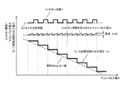
図3に従来のD/A変換回路13の出力電圧とチョッパ出力電力の関係を示す。横軸はチョッパ出力電圧である。チョッパ出力電圧に対するIlaしきい値の理想線は直線あるいは曲線になるが、D/A変換回路13の出力Vxはチョッパ出力電圧の変化に対して階段状に変化するため、理想線との誤差が発生する。その誤差がチョッパ出力電力の理想線との誤差ΔW1を発生させてしまう。
FIG. 3 shows the relationship between the output voltage of the conventional D /
図4に実施の形態1でのチョッパ出力電流波形とチョッパ出力電力を示す。単位時間あたりのチョッパ出力電力は、直流電源E、チョークコイルL1のインダクタンス、チョッパ出力電圧、スイッチング素子Q1のオン周期Tにより決定されるので、直流電源E、チョークコイルL1のインダクタンス、チョッパ出力電圧が同じであれば、周期TをT’(>T)へと長くするとチョッパ出力電力は低くなる。 FIG. 4 shows the chopper output current waveform and chopper output power in the first embodiment. Since the chopper output power per unit time is determined by the DC power supply E, the inductance of the choke coil L1, the chopper output voltage, and the ON period T of the switching element Q1, the DC power supply E, the inductance of the choke coil L1, and the chopper output voltage are If they are the same, increasing the period T to T ′ (> T) decreases the chopper output power.
図5にデジタル出力が一定である期間中のチョッパ出力電圧の増加に対してスイッチング素子Q1のオン周期Tを長くした実施の形態1でのチョッパ出力電力の変化を示す。図3に示すチョッパ出力電力の理想との誤差ΔW1が発生している場合において、図5に示すように、デジタル出力が一定である期間中のチョッパ出力電圧の増加に対してスイッチング素子Q1のオン周期Tを長くすることで、チョッパ出力電力は低くなるから、ΔW1>ΔW2となり、誤差を低減することができる。 FIG. 5 shows a change in the chopper output power in the first embodiment in which the ON period T of the switching element Q1 is increased with respect to the increase in the chopper output voltage during a period in which the digital output is constant. When the error ΔW1 from the ideal chopper output power shown in FIG. 3 occurs, as shown in FIG. 5, the switching element Q1 is turned on with respect to the increase of the chopper output voltage during a period when the digital output is constant. By increasing the period T, the chopper output power is reduced, so that ΔW1> ΔW2, and the error can be reduced.
(実施の形態2)
実施の形態2について以下に説明する。実施の形態1では、デジタル出力が一定である期間中のチョッパ出力電圧の増加に対してスイッチング素子Q1のオン周期Tを1段階だけ長くしたが、図6に示すように、デジタル出力が一定である期間中のチョッパ出力電圧の増加に対してスイッチング素子Q1のオン周期Tを複数段階にわたって長くすることで、更に安定したチョッパ出力電力を得ることができる。
(Embodiment 2)
The second embodiment will be described below. In the first embodiment, the ON period T of the switching element Q1 is increased by one step with respect to the increase of the chopper output voltage during a period in which the digital output is constant. However, as shown in FIG. 6, the digital output is constant. By increasing the ON period T of the switching element Q1 over a plurality of stages with respect to an increase in the chopper output voltage during a certain period, a more stable chopper output power can be obtained.
図6にデジタル出力が一定である期間中のチョッパ出力電圧の増加に対してスイッチング素子Q1のオン周期Tを複数段階に細分化して長くして行く実施の形態2でのチョッパ出力電力の変化を示す。図5に比べると、チョッパ出力電力の理想との誤差は更に小さくなり、実施の形態1でのチョッパ出力電力の理想との誤差ΔW2よりも、実施の形態2でのチョッパ出力電力の理想との誤差ΔW3のほうが小さく、ΔW2>ΔW3となり、更に理想のチョッパ出力電力に近づいた安定したチョッパ出力電力を得ることができる。 FIG. 6 shows the change in the chopper output power in the second embodiment in which the ON period T of the switching element Q1 is subdivided into a plurality of stages and lengthened with respect to the increase in the chopper output voltage during a period in which the digital output is constant. Show. Compared to FIG. 5, the error from the ideal of the chopper output power is further reduced, and the error ΔW2 from the ideal of the chopper output power in the first embodiment is smaller than the ideal of the chopper output power in the second embodiment. The error ΔW3 is smaller, ΔW2> ΔW3, and a stable chopper output power approaching the ideal chopper output power can be obtained.
(実施の形態3)
実施の形態3について以下に説明する。図7に実施の形態3でのチョッパ出力電流波形とチョッパ出力電力を示す。単位時間あたりのチョッパ出力電力は、直流電源E、チョークコイルL1のインダクタンス、チョッパ出力電圧、スイッチング素子Q1の周期Tにより決定されるので、直流電源E、チョークコイルL1のインダクタンス、チョッパ出力電圧が同じであれば、周期TをT”(<T)へと短くするとチョッパ出力電力は高くなる。
(Embodiment 3)
A third embodiment will be described below. FIG. 7 shows the chopper output current waveform and chopper output power in the third embodiment. Since the chopper output power per unit time is determined by the DC power supply E, the inductance of the choke coil L1, the chopper output voltage, and the cycle T of the switching element Q1, the DC power supply E, the inductance of the choke coil L1, and the chopper output voltage are the same. If the period T is shortened to T ″ (<T), the chopper output power increases.
図3のようにスイッチング周期を固定とする方式では、D/A変換回路の出力Vxが変化したときにチョッパ出力電力は急激に変化するため、チョッパ出力電力の理想との誤差ΔW1が瞬時に出力の変化として発生してしまう。そのためランプの光も同様に急激に変化し、不安定な光出力となってしまう。 In the method in which the switching period is fixed as shown in FIG. 3, since the chopper output power changes abruptly when the output Vx of the D / A converter circuit changes, an error ΔW1 from the ideal chopper output power is instantaneously output. Will occur as a change. For this reason, the light from the lamp also changes abruptly, resulting in an unstable light output.
図8にチョッパ出力電圧に対しスイッチング周期を変化させた実施の形態3でのチョッパ出力電力を示す。チョッパ出力電圧が増加してD/A変換回路の出力Vxが低く変化するときにスイッチング素子Q1のオン周期を短くすることで、チョッパ出力電力をD/A変換回路の出力Vxが低く変化する直前の値近傍まで高くする。その後、チョッパ出力電圧の増加に対して複数段階的にもとのオン周期まで戻し、更にもとのオン周期よりも複数段階的にオン周期を長くするように制御することで、急激なチョッパ出力電力の変化を抑制することができ、安定したチョッパ出力電力が得られ、安定した光出力を得ることができる。 FIG. 8 shows the chopper output power in the third embodiment in which the switching period is changed with respect to the chopper output voltage. By shortening the ON period of the switching element Q1 when the chopper output voltage increases and the output Vx of the D / A conversion circuit changes low, the chopper output power is reduced immediately before the output Vx of the D / A conversion circuit changes low. Increase to near the value of. After that, the chopper output voltage is abruptly increased by returning to the original on-cycle in multiple steps in response to the increase in chopper output voltage, and by further increasing the on-cycle in multiple steps from the original on-cycle. The change in power can be suppressed, stable chopper output power can be obtained, and stable light output can be obtained.
(実施の形態4)
実施の形態4について以下に説明する。上述の各実施の形態の放電灯点灯装置はプロジェクタの光源である高圧放電灯の点灯に用いられる。図9はプロジェクタの内部構成を示す概略図である。図中、31は投光窓、32は電源部、33a、33b、33cは冷却用ファン、34は外部信号入力部、35は光学系、36はメイン制御基板、40は放電灯点灯装置、Laは放電灯である。破線で示した枠内にメイン制御基板が実装されている。光学系35の途中には、放電灯Laからの光を透過または反射する画像表示手段(透過型液晶表示板または反射型画像表示素子)が設けられており、この画像表示手段を介する透過光または反射光をスクリーンに投射するように光学系35が設計されている。このように、放電灯点灯装置40は放電灯Laと共にプロジェクタ30の内部に実装されている。本発明の放電灯点灯装置を採用することにより、従来よりも小型で安価な構成で放電灯の光出力の精度や安定度を改善できる。
(Embodiment 4)
The fourth embodiment will be described below. The discharge lamp lighting device of each embodiment described above is used for lighting a high-pressure discharge lamp that is a light source of a projector. FIG. 9 is a schematic diagram showing the internal configuration of the projector. In the figure, 31 is a projection window, 32 is a power supply unit, 33a, 33b and 33c are cooling fans, 34 is an external signal input unit, 35 is an optical system, 36 is a main control board, 40 is a discharge lamp lighting device, La Is a discharge lamp. A main control board is mounted in a frame indicated by a broken line. In the middle of the optical system 35, image display means (a transmissive liquid crystal display panel or a reflective image display element) that transmits or reflects light from the discharge lamp La is provided. The optical system 35 is designed to project the reflected light onto the screen. Thus, the discharge lamp lighting device 40 is mounted inside the
E 直流電源
Q1 スイッチング素子
D1 ダイオード
C1 コンデンサ
L1 チョークコイル
R1 検出抵抗
La 放電灯
12 マイコン
13 D/A変換回路
Ila チョッパ出力電流の検出値
Vla チョッパ出力電圧の検出値
Vx D/A変換回路の出力電圧
E DC power source Q1 Switching element D1 Diode C1 Capacitor L1 Choke coil R1 Detection resistor
Claims (5)
Priority Applications (1)
| Application Number | Priority Date | Filing Date | Title |
|---|---|---|---|
| JP2006201351A JP4802906B2 (en) | 2006-07-24 | 2006-07-24 | Discharge lamp lighting device and projector |
Applications Claiming Priority (1)
| Application Number | Priority Date | Filing Date | Title |
|---|---|---|---|
| JP2006201351A JP4802906B2 (en) | 2006-07-24 | 2006-07-24 | Discharge lamp lighting device and projector |
Publications (2)
| Publication Number | Publication Date |
|---|---|
| JP2008027820A JP2008027820A (en) | 2008-02-07 |
| JP4802906B2 true JP4802906B2 (en) | 2011-10-26 |
Family
ID=39118231
Family Applications (1)
| Application Number | Title | Priority Date | Filing Date |
|---|---|---|---|
| JP2006201351A Expired - Fee Related JP4802906B2 (en) | 2006-07-24 | 2006-07-24 | Discharge lamp lighting device and projector |
Country Status (1)
| Country | Link |
|---|---|
| JP (1) | JP4802906B2 (en) |
Family Cites Families (4)
| Publication number | Priority date | Publication date | Assignee | Title |
|---|---|---|---|---|
| JPS4910207B1 (en) * | 1969-07-30 | 1974-03-08 | ||
| JPH01167998A (en) * | 1987-12-23 | 1989-07-03 | Matsushita Electric Works Ltd | Discharge lamp lighting device |
| JP2001297890A (en) * | 2000-04-13 | 2001-10-26 | Ikeda Electric Co Ltd | Electric discharge lamp lighting device |
| JP4241515B2 (en) * | 2004-06-10 | 2009-03-18 | パナソニック電工株式会社 | Discharge lamp lighting device and projector |
-
2006
- 2006-07-24 JP JP2006201351A patent/JP4802906B2/en not_active Expired - Fee Related
Also Published As
| Publication number | Publication date |
|---|---|
| JP2008027820A (en) | 2008-02-07 |
Similar Documents
| Publication | Publication Date | Title |
|---|---|---|
| JP5013108B2 (en) | Discharge lamp lighting device, control method therefor, and projector | |
| JP4434150B2 (en) | Discharge lamp lighting device and projector | |
| JP4940664B2 (en) | Discharge lamp lighting device and projector | |
| JP4518283B2 (en) | Discharge lamp lighting device, control method therefor, and projector | |
| JP4735239B2 (en) | Discharge lamp lighting device and image display device | |
| JP4462450B2 (en) | Discharge lamp lighting device, control method therefor, and projector | |
| JP2009508300A (en) | Method of operating a high intensity discharge lamp, lamp driver and projection system | |
| US8317339B2 (en) | Discharge lamp lighting device, projector, and control method of discharge lamp lighting device | |
| KR20010033383A (en) | Circuit for driving piezoelectric transformer | |
| US20100289429A1 (en) | Methods of and driving units for driving a gas discharge lamp | |
| US9363875B2 (en) | Discharge lamp lighting device, discharge lamp lighting method, and projector device | |
| JP4475433B2 (en) | Discharge lamp lighting control device and projector | |
| JP4802906B2 (en) | Discharge lamp lighting device and projector | |
| JP4175349B2 (en) | Discharge lamp lighting device and projector | |
| JP4710591B2 (en) | Discharge lamp lighting device and image display device | |
| JP4775003B2 (en) | Discharge lamp lighting device and image display device | |
| JP5537118B2 (en) | High pressure discharge lamp lighting device and image display device using the same | |
| JP4400872B2 (en) | Discharge lamp lighting device | |
| JP6558018B2 (en) | Discharge lamp driving device, light source device, projector, and discharge lamp driving method | |
| JP2003031394A (en) | Discharge lamp lighting device | |
| JP4748335B2 (en) | Discharge lamp lighting device, control method therefor, and projector | |
| JP5045947B2 (en) | Discharge lamp lighting control device and projector | |
| JP2005327661A (en) | Lighting device of high-pressure discharge lamp, and electronic apparatus using it | |
| JPH11305195A (en) | Method for indicating replacement time of back light lamp | |
| JP2017188314A (en) | Discharge lamp drive device, light source device, projector, and discharge lamp drive method |
Legal Events
| Date | Code | Title | Description |
|---|---|---|---|
| A621 | Written request for application examination |
Free format text: JAPANESE INTERMEDIATE CODE: A621 Effective date: 20090407 |
|
| A977 | Report on retrieval |
Free format text: JAPANESE INTERMEDIATE CODE: A971007 Effective date: 20101203 |
|
| A131 | Notification of reasons for refusal |
Free format text: JAPANESE INTERMEDIATE CODE: A131 Effective date: 20101221 |
|
| TRDD | Decision of grant or rejection written | ||
| A01 | Written decision to grant a patent or to grant a registration (utility model) |
Free format text: JAPANESE INTERMEDIATE CODE: A01 Effective date: 20110712 |
|
| A01 | Written decision to grant a patent or to grant a registration (utility model) |
Free format text: JAPANESE INTERMEDIATE CODE: A01 |
|
| A61 | First payment of annual fees (during grant procedure) |
Free format text: JAPANESE INTERMEDIATE CODE: A61 Effective date: 20110725 |
|
| R150 | Certificate of patent or registration of utility model |
Ref document number: 4802906 Country of ref document: JP Free format text: JAPANESE INTERMEDIATE CODE: R150 Free format text: JAPANESE INTERMEDIATE CODE: R150 |
|
| FPAY | Renewal fee payment (event date is renewal date of database) |
Free format text: PAYMENT UNTIL: 20140819 Year of fee payment: 3 |
|
| LAPS | Cancellation because of no payment of annual fees |