JP4732920B2 - Charging roll - Google Patents
Charging roll Download PDFInfo
- Publication number
- JP4732920B2 JP4732920B2 JP2006047176A JP2006047176A JP4732920B2 JP 4732920 B2 JP4732920 B2 JP 4732920B2 JP 2006047176 A JP2006047176 A JP 2006047176A JP 2006047176 A JP2006047176 A JP 2006047176A JP 4732920 B2 JP4732920 B2 JP 4732920B2
- Authority
- JP
- Japan
- Prior art keywords
- layer
- coating film
- rough surface
- charging roll
- forming particles
- Prior art date
- Legal status (The legal status is an assumption and is not a legal conclusion. Google has not performed a legal analysis and makes no representation as to the accuracy of the status listed.)
- Expired - Fee Related
Links
Images


Landscapes
- Electrostatic Charge, Transfer And Separation In Electrography (AREA)
- Rolls And Other Rotary Bodies (AREA)
Description
本発明は、複写機,プリンタ,ファクシミリ等の電子写真装置に用いられる帯電ロールに関するものである。 The present invention relates to a charging roll used in an electrophotographic apparatus such as a copying machine, a printer, and a facsimile machine.
一般に、電子写真複写機による複写は、つぎのようにして行われている。すなわち、まず、感光ドラムを帯電させ、その感光ドラム表面に原稿像を、光学系を介して投射し、光が投射された部分の帯電を打ち消すことにより、静電潜像を形成する。つぎに、上記静電潜像にトナーを付着させてトナー像を形成した後、このトナー像を、複写紙に転写して、複写画像を得るのである。 In general, copying by an electrophotographic copying machine is performed as follows. That is, first, a photosensitive drum is charged, a document image is projected onto the surface of the photosensitive drum via an optical system, and an electrostatic latent image is formed by canceling off the charging of the light projected portion. Next, after a toner is attached to the electrostatic latent image to form a toner image, the toner image is transferred to a copy sheet to obtain a copy image.
上記静電潜像の形成に先立って感光ドラム表面を帯電させる方式としては、近年、帯電ロールによる帯電方式が多く採用されている。そして、上記帯電方式に用いられる帯電ロールとしては、例えば、軸体の外周に、導電性弾性体からなる抵抗調整層が形成され、さらにその外周に、塗膜により保護層を形成したものが知られている。 As a method for charging the surface of the photosensitive drum prior to the formation of the electrostatic latent image, in recent years, a charging method using a charging roll has been widely employed. As a charging roll used in the above charging method, for example, a roll in which a resistance adjusting layer made of a conductive elastic body is formed on the outer periphery of the shaft body, and a protective layer is formed on the outer periphery thereof by a coating film is known. It has been.
上記保護層は、通常、ポリアミド系樹脂、フッ素系樹脂、アクリル樹脂、ウレタン樹脂等の樹脂を主成分とする材料に導電剤を配合したものを、有機溶剤に溶解もしくは分散してコーティング液とし、これを、上記抵抗調整層の外周に、薄く塗工することによって得られる。しかし、上記コーティング液塗工時に、導電剤が沈殿する等の理由から、塗膜に含有される導電剤に偏りが生じ、場所によっては、導電剤を殆ど含まないスキン層が形成される場合がある。 The protective layer is usually a coating liquid prepared by dissolving or dispersing a conductive agent in a material mainly composed of a resin such as a polyamide resin, a fluorine resin, an acrylic resin, or a urethane resin in an organic solvent, This is obtained by thinly coating the outer periphery of the resistance adjusting layer. However, when the coating liquid is applied, the conductive agent contained in the coating film is biased for reasons such as precipitation of the conductive agent, and depending on the location, a skin layer containing almost no conductive agent may be formed. is there.
このように、保護層に、部分的にスキン層が形成されると、帯電むらが生じたり、ロールへの印加をオフにしてもロール表面に電荷が残留したりするため、耐久劣化後に画像の不具合を招きやすいという問題がある。また、帯電性能が不充分であると、この帯電ロールを組み込んだ電子写真複写機等における電源コストが高くなり、経済的に好ましくないという問題もある。 As described above, when the skin layer is partially formed on the protective layer, uneven charging occurs, or even if the application to the roll is turned off, the charge remains on the roll surface. There is a problem that it is easy to cause a defect. Further, if the charging performance is insufficient, the power supply cost in an electrophotographic copying machine or the like incorporating this charging roll becomes high, which is not economically preferable.
そこで、このようなスキン層の形成を防止し、保護層表面に適度な凹凸を形成して帯電性能を向上させることが検討されている。例えば、図4に示すように、保護層3に、大粒径の粒子4と小粒径の粒子5の2種類の粒子を添加して、その表面に凹凸を形成したものが提案されている(例えば特許文献1参照)。なお、2は抵抗調整層(弾性層)である。
しかしながら、上記のように、大小2種類の粒子4、5を保護層3に含有させるには、保護層3の膜厚を比較的厚くせざるを得ず、表面抵抗と体積抵抗の差が大きくなるため、帯電性能、耐久劣化後の画像評価において、要求されるような優れた特性のものは得られていないのが実情である。
However, as described above, in order to contain the two kinds of large and
本発明は、このような事情に鑑みなされたもので、優れた帯電性能を備え、長期にわたって良好な画像を得ることのできる帯電ロールの提供を、その目的とする。 The present invention has been made in view of such circumstances, and an object thereof is to provide a charging roll having excellent charging performance and capable of obtaining a good image over a long period of time.
上記の目的を達成するため、本発明は、軸体と、上記軸体の外周に、直接もしくは他の層を介して形成される抵抗調整層と、上記抵抗調整層の外周に形成される表層塗膜とを備えた帯電ロールであって、上記抵抗調整層の表面が凹凸粗面に形成され、粗面形成用粒子が、その一部を上記抵抗調整層表面の凹部内に嵌入させ他の部分を上記抵抗調整層表面から突出させた状態で、上記表層塗膜を介して抵抗調整層に固着されており、上記表層塗膜の厚みが4μm以下で、上記粗面形成用粒子の表層塗膜からの理論露出率が50%以上に設定されている帯電ロールを第1の要旨とする。 In order to achieve the above object, the present invention provides a shaft body, a resistance adjusting layer formed on the outer periphery of the shaft body directly or via another layer, and a surface layer formed on the outer periphery of the resistance adjusting layer. A charging roll provided with a coating film, wherein the surface of the resistance adjustment layer is formed into an uneven rough surface, and the rough surface forming particles are partially inserted into the recesses of the surface of the resistance adjustment layer. With the portion protruding from the surface of the resistance adjustment layer, it is fixed to the resistance adjustment layer via the surface coating film, and the surface coating film has a thickness of 4 μm or less and the surface coating of the rough surface forming particles. The charging roll in which the theoretical exposure rate from the film is set to 50% or more is set as a first gist.
また、本発明は、そのなかでも、特に、上記抵抗調整層の表面粗さ(Ra)が0.5〜1.0μmに設定され、上記粗面形成用粒子の平均粒径が3〜6μmに設定されている帯電ロールを第2の要旨とし、上記抵抗調整層の表面粗さ(Ra)が1.0μm〜2.0μmに設定され、上記粗面形成用粒子の平均粒径が5〜8μmに設定されている帯電ロールを第3の要旨とする。 In the present invention, in particular, the surface roughness (Ra) of the resistance adjusting layer is set to 0.5 to 1.0 μm, and the average particle size of the rough surface forming particles is 3 to 6 μm. The charging roll that has been set is a second gist, the surface roughness (Ra) of the resistance adjustment layer is set to 1.0 μm to 2.0 μm, and the average particle size of the rough surface forming particles is 5 to 8 μm. The charging roll set to 1 is set as a third gist.
すなわち、本発明者らは、前記課題を解決するため鋭意研究を重ね、その過程で、帯電ロールの帯電性能および耐久劣化後の画像評価を向上させるには、最外層である保護層の厚みをできるだけ薄くするとともに、感光ドラムと帯電ロールの外周面との接触面積を減少させ、その隙間において一定の放電領域を確保することが必要であるとの知見を得た。そこで、保護層の厚みをごく薄く設定することができ、しかも感光ドラムとの接触面積を減少させることのできる帯電ロールの表面構造について、さらに研究を重ねた結果、抵抗調整層の表面を、凹凸粗面に形成し、その上に、4μm以下のごく薄い表層塗膜を形成するとともに、その表層塗膜を介して、粗面形成用粒子を、その一部を上記抵抗調整層表面の凹部内に嵌入させ他の部分を上記抵抗調整層表面から突出させた状態で固着させ、このときの粗面形成用粒子の表層塗膜からの理論露出率が50%以上となるよう設定すると、粗面形成用粒子によって均一な凹凸粗面が形成され、また、上記粗面形成用粒子と抵抗調整層凹部の底部との間に空隙が形成され、その空隙によって、放電領域がより大きくなるため、非常に均一で安定した帯電性能を備えた帯電ロールが得られることを見いだし、本発明に到達した。 That is, the present inventors have conducted intensive research to solve the above problems, and in the process, in order to improve the charging performance of the charging roll and the image evaluation after durability deterioration, the thickness of the protective layer that is the outermost layer is reduced. It has been found that it is necessary to make the thickness as thin as possible, reduce the contact area between the photosensitive drum and the outer peripheral surface of the charging roll, and ensure a certain discharge area in the gap. Therefore, as a result of further research on the surface structure of the charging roll that can reduce the contact area with the photosensitive drum, the thickness of the protective layer can be set very thin. Formed on the rough surface, and a very thin surface coating film of 4 μm or less is formed on the rough surface. Through the surface coating film, a part of the rough surface forming particles is formed in the recesses on the surface of the resistance adjusting layer. When the other portion is fixed in a state of protruding from the surface of the resistance adjusting layer, and the theoretical exposure rate from the surface coating film of the rough surface forming particles at this time is set to be 50% or more, the rough surface A uniform uneven rough surface is formed by the forming particles, and a gap is formed between the rough surface forming particles and the bottom of the recess of the resistance adjustment layer. Uniform and stable It found that charging roll having a conductive performance can be obtained, thereby achieving the present invention.
本発明の帯電ロールは、内側に設けられる抵抗調整層の表面を、凹凸粗面に形成し、その上に、4μm以下のごく薄い表層塗膜を形成するとともに、その表層塗膜を介して、粗面形成用粒子を、その一部を上記抵抗調整層表面の凹部内に嵌入させ他の部分を上記抵抗調整層表面から突出させた状態で固着させ、このときの粗面形成用粒子の表層塗膜からの理論露出率が50%以上となるよう設定したものである。この構成によれば、粗面形成用粒子によって均一な凹凸粗面が形成され、また、上記粗面形成用粒子と抵抗調整層凹部の底部との間に空隙が形成されて放電領域が増大している。したがって、従来のような帯電むらが生じず、非常に均一で安定した帯電性能を備えた帯電ロールとなる。 The charging roll of the present invention forms the surface of the resistance adjusting layer provided on the inner side on a rough surface, and forms a very thin surface coating film of 4 μm or less on the surface, and through the surface coating film, The rough surface-forming particles are fixed in a state in which a part thereof is fitted into the recesses on the surface of the resistance adjusting layer and the other part is protruded from the surface of the resistance adjusting layer. The theoretical exposure rate from the coating film is set to be 50% or more. According to this configuration, a uniform rough surface is formed by the rough surface forming particles, and a gap is formed between the rough surface forming particles and the bottom of the resistance adjustment layer recess to increase the discharge region. ing. Therefore, a charging roll having a very uniform and stable charging performance without causing uneven charging as in the prior art is obtained.
そして、本発明の帯電ロールを用いて得られる画像は、長期にわたって画像不具合を発生することなく、良好である。さらに、優れた帯電性能を備えているため、これを組み込んだ装置において、電源コストの低減化を実現することができる。 The image obtained using the charging roll of the present invention is good without causing image defects over a long period of time. Furthermore, since it has excellent charging performance, it is possible to achieve a reduction in power supply cost in an apparatus incorporating the charging performance.
なお、本発明の帯電ロールのなかでも、特に、上記抵抗調整層の表面粗さ(Ra)が0.5〜1.0μmに設定され、上記粗面形成用粒子の平均粒径が3〜6μmに設定されているもの、あるいは、特に、上記抵抗調整層の表面粗さ(Ra)が1.0μm〜2.0μmに設定され、上記粗面形成用粒子の平均粒径が5〜8μmに設定されているものは、とりわけ優れた帯電性能を備えている。 Note that, among the charging rolls of the present invention, in particular, the surface roughness (Ra) of the resistance adjusting layer is set to 0.5 to 1.0 μm, and the average particle diameter of the rough surface forming particles is 3 to 6 μm. Or, in particular, the surface roughness (Ra) of the resistance adjusting layer is set to 1.0 μm to 2.0 μm, and the average particle size of the rough surface forming particles is set to 5 to 8 μm. What has been provided has particularly good charging performance.
つぎに、本発明の実施の形態について説明する。ただし、本発明は、この実施の形態に限られるものではない。 Next, an embodiment of the present invention will be described. However, the present invention is not limited to this embodiment.
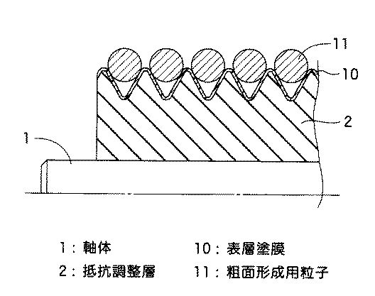
本発明の帯電ロールは、例えば、図1に示すように、軸体1の外周面に沿って抵抗調整層2が形成され、さらに上記抵抗調整層2の外周面に、表層塗膜10が形成された構成になっている。
In the charging roll of the present invention, for example, as shown in FIG. 1, the
より詳しく説明すると、上記抵抗調整層2の表面は、その模式的な拡大断面図である図2に示すように、凹凸粗面に形成されており、その凹凸に沿って、非常に薄い表層塗膜10が形成されている。そして、上記表層塗膜10を介して、粗面形成用粒子11が、その一部を上記抵抗調整層2表面の凹部内に嵌入させ他の部分を上記抵抗調整層2表面から突出させた状態で、抵抗調整層2に固着されている。
More specifically, the surface of the
上記帯電ロールの軸体1としては、特に限定されるものではなく、中実体であっても、中空円筒体であってもよい。そして、その形成材料についても、特に限定されず、例えば、アルミニウム、ステンレス等の金属材料等があげられる。なお、必要に応じ、軸体1の表面に接着剤、プライマー等を塗布してもよい。また、接着剤、プライマー等には、必要に応じて導電化を行ってもよい。
The
上記軸体1の外周面に形成される抵抗調整層2の形成材料としては、特に限定されるものではなく、例えば、ポリウレタン系エラストマー、ヒドリンゴム(ECO等)、スチレン−ブタジエンゴム(SBR)、ポリノルボルネンゴム、エチレン−プロピレン−ジエンゴム(EPDM)、アクリロニトリル−ブタジエンゴム(NBR)、水素化アクリロニトリル−ブタジエンゴム(H−NBR)、ブタジエンゴム(BR)、イソプレンゴム(IR)、天然ゴム(NR)、シリコーンゴム等があげられ、単独で用いても二種以上を併用してもよい。
The material for forming the
そして、上記抵抗調整層2の形成材料には、導電性付与のため、カーボンブラック、グラファイト、チタン酸カリウム、酸化鉄、c−TiO2 、c−ZnO、c−SnO2 、イオン導電剤(トリメチルオクタデシルアンモニウムパークロレート,ベンジルトリメチルアンモニウムクロリド等の四級アンモニウム塩、ホウ酸塩、過塩素酸リチウム、過塩素酸カリウム等の構造電荷特異性陰イオン、界面活性剤等)等の従来公知の導電剤が、適宜添加される。さらに、必要に応じて、発泡剤、架橋剤、架橋促進剤、オイル等を適宜添加してもよい。
The material for forming the
上記抵抗調整層2の形成材料は、例えば、その各成分をニーダー等の混練機によって混練することにより、調製することができる。
The material for forming the
また、上記抵抗調整層2の外周面に形成される表層塗膜10の形成材料としては、特に限定されるものではなく、ウレタン系樹脂、アクリル系樹脂、オレフィン系樹脂、エポキシ系樹脂、ポリアミド系樹脂、ポリエステル系樹脂、アクリルフッ素系樹脂、シリコーン変性アクリル系樹脂、フッ素化オレフィン系樹脂等、従来から帯電ロールの最外層(保護層)として用いられているものであれば、どのような種類であっても差し支えない。そして、これらは単独で用いても、二種以上を併用してもよい。また、導電性付与のため、カーボンブラック、金属酸化物、四級アンモニウム塩、ホウ酸塩、過塩素酸リチウム等の導電剤が、上記材料中に適宜添加される。さらに、必要に応じて、充填剤、安定剤、紫外線吸収剤、帯電防止剤、補強剤、滑剤、離型剤、染料、顔料、難燃剤、オイル等を適宜に配合することができる。
Moreover, it does not specifically limit as a formation material of the surface
さらに、上記表層塗膜10を介して前記抵抗調整層2の表面に固着される粗面形成用粒子11も、その材質は特に限定されるものではなく、例えば、シリカ、ウレタン樹脂、ポリアミド樹脂、フッ素樹脂、アクリル樹脂、メタクリル樹脂、尿素樹脂等があげられる。これらは、単独で用いてもよいし、2種以上を併用してもよい。ただし、抵抗調整層2の凹凸粗面に、図2に示すように固着させるには、上記抵抗調整層2の凹凸粗面の凹凸の大きさに対し、適度の粒径に設定されていることが好ましく、しかもできるだけ粒径の揃ったものを用いることが望ましい。
Furthermore, the material for the rough surface forming particles 11 fixed to the surface of the
なお、上記表層塗膜10の形成材料は、有機溶剤に溶解され、これに、上記粗面形成用粒子11を分散することによりコーティング液として調製されるようになっている。上記有機溶剤としては、メチルエチルケトン(MEK)、メタノール、トルエン、イソプロピルアルコール、メチルセロソルブ、ジメチルホルムアミド等があげられる。これらは単独であるいは二種以上併せて用いられる。
In addition, the formation material of the said surface
本発明の帯電ロールは、これらの材料を用いて、例えば、つぎのようにして作製することができる。 The charging roll of the present invention can be produced using these materials as follows, for example.
まず、芯金となる軸体1を用意し、その外周面に接着剤を塗布し、抵抗調整層2形成用の金型内に装着する。そして、ニーダー等の混練機で混練した抵抗調整層2形成材料を、金型内に注型した後、金型を閉じて加熱処理(130〜200℃×20〜90分)して、抵抗調整層2を架橋硬化させる。そして、上記金型から脱型することにより、軸体1の外周面に抵抗調整層2が形成されたロールを取り出す。
First, the
つぎに、上記ロールにおける抵抗調整層2の外周面に凹凸形状を付与して粗面化する。粗面化の方法としては、特に限定するものではないが、例えば、研磨処理、ブラスト処理、レーザーエッチング、プラズマエッチング等があげられる。また、このように、抵抗調整層2の成形後、その表面を粗面化する方法以外に、例えば、抵抗調整層2を金型成形する際、予めその金型の内周面を、研磨等により粗面化しておき、これを抵抗調整層2の成形面に転写することにより、成形と粗面化を一工程で行うようにしてもよい。さらに、抵抗調整層2の形成材料に、予め粗面形成用粒子を配合しておき、上記粗面形成用粒子に由来する凹凸が、抵抗調整層2の表面に形成されるようにしてもよい。
Next, an uneven shape is imparted to the outer peripheral surface of the
上記粗面化によって得られる抵抗調整層2の表面粗さ(Ra)は、表層塗膜10を介して粗面形成用粒子11を固着させることと、帯電性能とを考慮して、0.5〜2.0μmに設定することが好適である。
The surface roughness (Ra) of the
なお、上記表面粗さ(Ra)は、JIS B0601:1994に従って求められるもので、接触式表面粗さ計(サーフコム480A、東京精密社製)を用い、下記の測定条件で測定される9点の測定値を平均した値である。
〔測定条件〕
触針径 :2μm
押し付け圧 :0.7mN
測定速度 :0.3mm/sec
測定倍率 :5000倍
カットオフ波長:0.8mm
測定長さ :2.5mm
測定個所 :軸方向3点×周方向3点の9点
In addition, the said surface roughness (Ra) is calculated | required according to JISB0601: 1994, 9 points | pieces measured on the following measurement conditions using a contact-type surface roughness meter (Surfcom 480A, Tokyo Seimitsu Co., Ltd.). It is a value obtained by averaging measured values.
〔Measurement condition〕
Stylus diameter: 2 μm
Pressing pressure: 0.7mN
Measurement speed: 0.3 mm / sec
Measurement magnification: 5000 times Cut-off wavelength: 0.8 mm
Measurement length: 2.5mm
Measurement points: 9 points in the axial direction x 3 points in the circumferential direction
つぎに、上記粗面化された抵抗調整層2の外周面に、表層塗膜10形成用のコーティング液(粗面形成用粒子11を分散させたもの)を塗工する。塗工方法は、特に制限するものではなく、ディッピング法、スプレー法、ロールコート法等の従来の方法が適用できる。そして、塗工後、乾燥(40℃×30分程度)および加熱処理(加硫処理、100〜200℃×20〜90分)を行うことにより、表層塗膜10を形成する。このようにして、図2に示すような、粗面形成用粒子11が、その一部を上記抵抗調整層2の凹部内に嵌入させ他の部分を上記抵抗調整層2の表面から突出させた状態で、上記表層塗膜10を介して抵抗調整層2に固着された、特殊な構造の帯電ロールを作製することができる。
Next, a coating liquid for forming the surface coating film 10 (in which the rough surface forming particles 11 are dispersed) is applied to the outer peripheral surface of the roughened
なお、上記表層塗膜10の膜厚は、4μm以下となるよう設定しなければならない。すなわち、膜厚が4μmを超えると、得られる帯電ロール表面への残留電荷量が増えて応答性が悪くなり、帯電性能が下がるからである。
The film thickness of the
そして、上記表層塗膜10からの粗面形成用粒子11の理論露出率が50%以上になるように、粗面形成用粒子11を、表層塗膜10を介して抵抗調整層2に固着させなければならない。すなわち、上記理論露出率が50%未満では、表層塗膜10の表面(=帯電ロール表面)から上に突出する粗面形成用粒子11の高さが低くなり、この粗面形成用粒子11の根元部と、抵抗調整層2表面の凹部との間に形成される空隙が小さくなり、この部分を放電領域として利用する効果が小さくなるからである。
Then, the rough surface forming particles 11 are fixed to the
なお、上記粗面形成用粒子11の理論露出率は、下記の式(1)で求めることができる。 The theoretical exposure rate of the rough surface forming particles 11 can be obtained by the following equation (1).
また、上記表層塗膜10からの粗面形成用粒子11の理論露出率を50%以上にするには、表層塗膜10形成用の塗膜材料と粗面形成用粒子11を用いてコーティング液を調製する際、その組成および粗面形成用粒子11の大きさを適宜調製する必要がある。特に、形成用粒子11の粒径は、抵抗調整層2の表面粗さ(Ra)の程度も考慮して選択することが望ましい。ちなみに、抵抗調整層2の表面粗さ(Ra)が0.5〜1.0μmの場合、粗面形成用粒子11は、平均粒径が3〜6μmのものを用いることが好ましく、抵抗調整層の表面粗さ(Ra)が1.0〜2.0μmの場合、平均粒径が5〜8μmのものを用いることが好ましい。
Further, in order to increase the theoretical exposure rate of the rough surface forming particles 11 from the
なお、本発明において、上記粗面形成用粒子11の平均粒径は、母集団から任意に抽出される試料を用いて導出される値である。また、粒子形状が真球状ではなく楕円球状(断面が楕円の球)等のように一律に粒径が定まらない場合には、最長径と最短径との単純平均値をその粒子の粒径とする。 In the present invention, the average particle diameter of the rough surface forming particles 11 is a value derived using a sample arbitrarily extracted from the population. In addition, if the particle size is not uniform, as in the case of a particle shape that is not a true sphere but an elliptical sphere (a sphere with an elliptical cross section), the simple average value of the longest diameter and the shortest diameter is the particle diameter of the particle. To do.
このようにして得られる帯電ロールは、内側に設けられる抵抗調整層2の表面が、凹凸粗面に形成され、その上に、4μm以下のごく薄い表層塗膜10が形成されており、その表層塗膜10を介して、粗面形成用粒子11が、その一部を上記抵抗調整層2表面の凹部内に嵌入させ他の部分を上記抵抗調整層2表面から突出させた状態で固着されて、粗面形成用粒子11の表層塗膜10からの理論露出率が50%以上となるよう設定されている。このため、上記粗面形成用粒子11によって帯電ロール表面に均一な凹凸粗面が形成され、また、上記粗面形成用粒子11と抵抗調整層2凹部の底部との間に形成される空隙によって、放電領域がより大きくなるため、非常に均一で安定した帯電性能を備えたものとなる。
In the charging roll thus obtained, the surface of the
したがって、上記帯電ロールを用いて得られる画像は、長期にわたって画像不具合を発生することなく、良好である。さらに、優れた帯電性能を備えているため、これを組み込んだ装置において、電源コストの低減化を実現することができる。 Therefore, an image obtained using the charging roll is good without causing image defects over a long period of time. Furthermore, since it has excellent charging performance, it is possible to achieve a reduction in power supply cost in an apparatus incorporating the charging performance.
なお、上記抵抗調整層2の厚みは、特に限定されるものではなく、要求される形態、特性に応じて、適宜に設定される。
The thickness of the
そして、本発明の帯電ロールは、図1に示すような2層構造のものに限定されるものでなく、例えば、軸体1と抵抗調整層2の間に、導電性弾性体層や軟化剤移行防止層等を、必要に応じて適宜設けることができる。
The charging roll of the present invention is not limited to the two-layer structure as shown in FIG. 1. For example, a conductive elastic layer or softening agent is provided between the
つぎに、実施例について比較例と併せて説明する。 Next, examples will be described together with comparative examples.
〔実施例1〕
まず、下記のとおり、抵抗調整層形成材料と表層塗膜形成材料(組成イ)と粗面形成用粒子aとを準備した。そして、それらを用いて、後記の方法にしたがって、帯電ロールを作製した。
[Example 1]
First, a resistance adjusting layer forming material, a surface layer coating film forming material (composition A), and rough surface forming particles a were prepared as described below. And using them, the charging roll was produced according to the method of a postscript.
〔抵抗調整層形成材料の組成〕
ヒドリンゴム(ダイソー社製、エピクロマーCG102 ) 100 重量部
ステアリン酸(花王社製、ルナックS30) 1 〃
酸化亜鉛2種 5 〃
ハイドロタルサイト(協和化学社製、DHT−4A) 3 〃
粉末イオウ(鶴見化学社製) 1.5 〃
加硫促進剤(大内新興化学工業社製、ノクセラーDM) 1.5 〃
〃 (大内新興化学工業社製、ノクセラーTS) 0.5 〃
イオン導電剤(トリメチルオクタデシルアンモニウムパークロレート)1 〃
[Composition of resistance adjustment layer forming material]
Hydrin rubber (Daiso Corporation, Epichromer CG102) 100 parts by weight Stearic acid (Kao Corporation, Lunac S30) 1 〃
Hydrotalcite (DHT-4A, manufactured by Kyowa Chemical Co., Ltd.) 3
Powder sulfur (manufactured by Tsurumi Chemical Co., Ltd.) 1.5 〃
Vulcanization accelerator (Ouchi Shinsei Chemical Co., Ltd., Noxeller DM) 1.5 〃
〃 (Ouchi Shinsei Chemical Co., Ltd., Noxeller TS) 0.5 〃
Ionic conductive agent (trimethyl octadecyl ammonium perchlorate) 1 〃
〔表層塗膜形成材料の組成イ〕
ポリアミド樹脂(ナガセケムテックス社製、トレジンEF30T) 100重量部
イオン導電剤(トリメチルオクタデシルアンモニウムパークロレート) 1 〃
メタノール/蒸留水=3/1の混合溶剤(有効成分が5重量%となるよう調製)
[Composition of surface coating film forming material]
Polyamide resin (manufactured by Nagase ChemteX Corporation, Toresin EF30T) 100 parts by weight Ionic conductive agent (trimethyloctadecyl ammonium perchlorate) 1 〃
Mixed solvent of methanol / distilled water = 3/1 (prepared so that the active ingredient is 5% by weight)
〔粗面形成用粒子a〕
平均粒径8μmのウレタン粒子(大日精化社製、ダイミックビーズUCN5070D)
[Rough surface forming particles a]
Urethane particles with an average particle diameter of 8 μm (Daimic Beads UCN5070D, manufactured by Dainichi Seika Co., Ltd.)
〔帯電ロールの作製〕
まず、前記抵抗調整層形成材料を、バンバリーミキサーにて混練りして、成型用のゴム材料を得た。また、上記表層塗膜形成材料によって調製された液に、上記粗面形成用粒子であるウレタンビーズを、ポリアミド樹脂100重量部に対し30重量部となる割合で配合して分散させることにより、コーティング液を得た。
[Preparation of charging roll]
First, the resistance adjusting layer forming material was kneaded with a Banbury mixer to obtain a rubber material for molding. In addition, by coating and dispersing the urethane beads, which are the rough surface forming particles, in a ratio of 30 parts by weight with respect to 100 parts by weight of the polyamide resin in the liquid prepared from the surface layer coating material, coating is performed. A liquid was obtained.
そして、直径6mmの芯金を用意し、その外周面に接着剤を塗布した後、所定の金型内に装填し、金型内の中空部に、前記抵抗調整層形成材料を注型した。そして、金型を閉じて、加熱処理(一次加硫150℃×30分、二次加硫160℃×60分)を行うことにより加硫硬化させ、上記金型から脱型することにより、芯金の外周面に抵抗調整層が形成されたロール中間体を取り出した。なお、この抵抗調整層の厚みは1.5mmであった。 Then, a core metal having a diameter of 6 mm was prepared, and an adhesive was applied to the outer peripheral surface thereof. Then, the core metal was loaded into a predetermined mold, and the resistance adjusting layer forming material was cast into a hollow portion in the mold. Then, the mold is closed, vulcanized and cured by heat treatment (primary vulcanization 150 ° C. × 30 minutes, secondary vulcanization 160 ° C. × 60 minutes), and demolded from the mold, thereby obtaining a core. The roll intermediate body in which the resistance adjusting layer was formed on the outer peripheral surface of gold was taken out. In addition, the thickness of this resistance adjustment layer was 1.5 mm.
そして、上記抵抗調整層の表面に対し、その表面粗さ(Ra)が1.5μmとなるよう研磨処理を行った後、その外周面に、前記コーティング液を、乾燥後の表層塗膜の厚みが2.0μmとなるようロールコート法により塗工した。その後、乾燥(40℃×30分)および加熱処理(120℃×30分)を行うことにより、表層塗膜を形成して、図1に示す2層構造の帯電ロールを作製した。 Then, after polishing the surface of the resistance adjusting layer so that the surface roughness (Ra) is 1.5 μm, the coating liquid is applied to the outer peripheral surface of the surface coating film after drying. Was applied by a roll coating method so as to be 2.0 μm. Thereafter, drying (40 ° C. × 30 minutes) and heat treatment (120 ° C. × 30 minutes) were performed to form a surface layer coating film, and a charging roll having a two-layer structure shown in FIG. 1 was produced.
〔実施例2〜11、比較例1〜3〕
上記実施例1とは異なる、下記の3種類の組成ロ〜ニからなる表層塗膜形成材料を用意した。また、上記実施例1とは異なる、後記の4種類の粗面形成用粒子b〜eを用意した。
[Examples 2 to 11, Comparative Examples 1 to 3]
A surface coating film forming material comprising the following three types of compositions different from Example 1 was prepared. Also, the following four types of rough surface forming particles b to e, which are different from those of Example 1, were prepared.
〔表層塗膜形成材料の組成ロ〕
NBR(アクリロニトリル量34%:JSR社製、N231H) 50重量部
レゾール型フェノール樹脂(住友デュレズ社製,スミライトレジンPR−175)
50重量部
イオン導電剤(トリメチルオクタデシルアンモニウムパークロレート) 1 〃
MEK(有効成分が3重量%となるよう調製)
[Composition of surface coating film forming material]
NBR (acrylonitrile amount 34%: manufactured by JSR, N231H) 50 parts by weight resol type phenolic resin (manufactured by Sumitomo Durez, Sumilite Resin PR-175)
50 parts by weight ionic conductive agent (trimethyloctadecyl ammonium perchlorate) 1 〃
MEK (prepared so that the active ingredient is 3% by weight)
〔表層塗膜形成材料の組成ハ〕
フッ素変性アクリル樹脂(大日本インキ化学工業社製、ディフェンサTR230K)
100重量部
イオン導電剤(トリメチルオクタデシルアンモニウムパークロレート) 1 〃
MEK(有効成分が3重量%となるよう調製)
[Composition of surface layer coating material]
Fluorine-modified acrylic resin (Dai Nippon Ink Chemical Co., Ltd., Defensor TR230K)
100 parts by weight ionic conductive agent (trimethyloctadecyl ammonium perchlorate) 1 〃
MEK (prepared so that the active ingredient is 3% by weight)
〔表層塗膜形成材料の組成ニ〕
エチレンオキサイド含有光重合性モノマー(ポリエチレングリコールジアクリレート: 新中村化学工業社製) 40重量部
環状不飽和化合物エチレンオキサイド含有光重合性モノマー(ビスフェノールA エチ レンオキサイド変性ジアクリレート、m+n≒20:新中村化学工業社製)
60重量部
イオン導電剤(トリメチルオクタデシルアンモニウムパークロレート) 3 〃
光重合開始剤(千葉スペシャリティーケミカルズ社製) 1 〃
MEK(有効成分が3重量%となるよう調製)
[Composition of surface coating film forming material]
Ethylene oxide-containing photopolymerizable monomer (polyethylene glycol diacrylate: Shin-Nakamura Chemical Co., Ltd.) 40 parts by weight Cyclic unsaturated compound ethylene oxide-containing photopolymerizable monomer (bisphenol A ethylene oxide-modified diacrylate, m + n≈20: Shin-Nakamura (Made by Chemical Industries)
60 parts by weight ionic conductive agent (trimethyloctadecyl ammonium perchlorate) 3 〃
Photopolymerization initiator (Chiba Specialty Chemicals) 1 〃
MEK (prepared so that the active ingredient is 3% by weight)
〔粗面形成用粒子b〕
平均粒径4μmの多孔質球形シリカ(富士シリシア社製、サイロスフィアC−1504 )
[Rough surface forming particles b]
Porous spherical silica with an average particle diameter of 4 μm (Fuji Silysia Co., Ltd., Cyrossphere C-1504)
〔粗面形成用粒子c〕
平均粒径3μmのPMMA粒子(綜研化学社製、ケミスノーMX300)
[Rough surface forming particles c]
PMMA particles with an average particle size of 3 μm (Kemisnow MX300, manufactured by Soken Chemical Co., Ltd.)
〔粗面形成用粒子d〕
平均粒径1.5μmのPMMA粒子(綜研化学社製、ケミスノーMX150)
[Rough surface forming particles d]
PMMA particles with an average particle size of 1.5 μm (Chemical Chemical Co., Chemisnow MX150)
〔粗面形成用粒子e〕
平均粒径10μmの多孔質球形シリカ(富士シリシア社製、サイロスフィアC−151 0)
[Rough surface forming particles e]
Porous spherical silica having an average particle size of 10 μm (Fuji Silysia Co., Ltd., Cyrossphere C-1510)
そして、各帯電ロールの抵抗調整層の表面粗さ、表層塗膜の形成材料組成、塗膜厚み、粗面形成用粒子の種類等を変えることにより、後記の表1〜表4に示す構成的特徴を備えた10種類の実施例品(2〜11)と、3種類の比較例品(1〜3)を得た。なお、実施例9における表層塗膜形成時の加熱処理条件は160℃×30分、実施例10、実施例11における表層塗膜形成時の加熱処理条件は100℃×30分である。それ以外は、特に明記する以外は、各例とも同一形成材料、同一条件で作製されている。また、前記実施例1についても、後記の表1に併せて示した。 Then, by changing the surface roughness of the resistance adjusting layer of each charging roll, the composition of the surface coating film, the thickness of the coating film, the type of particles for forming the rough surface, etc. Ten types of example products (2-11) having characteristics and three types of comparative products (1-3) were obtained. In addition, the heat processing conditions at the time of surface layer coating film formation in Example 9 are 160 degreeC x 30 minutes, and the heat processing conditions at the time of surface layer coating film formation in Example 10 and Example 11 are 100 degreeC x 30 minutes. Other than that, unless otherwise specified, each example is manufactured under the same forming material and under the same conditions. Further, Example 1 is also shown in Table 1 below.
このようにして得られた各帯電ロールについて、下記の方法にしたがって、その帯電性能評価と、耐久後の画像評価と、粒子脱落性評価とを行い、その結果を後記の表1〜表4に併せて示した。 For each charging roll thus obtained, according to the following method, the charging performance evaluation, the image evaluation after durability, and the particle dropout evaluation are performed, and the results are shown in Tables 1 to 4 below. Also shown.
〔帯電性能評価〕
図3に示すように、実際の感光ドラム20に帯電ロール21を組み付け、帯電ロール21に、高圧電源22からアンプ23を介して−1.2kVの電圧を印加した。そして、上記感光ドラム20を1/4周だけ回転させた後のドラム電位量を、軸方向に移動して連続的にその表面電位を測定する高圧プローブ24を備えた電位測定器(図示せず)を用いて測定した。そして、下記の式(2)によって、電位量のばらつき(V)を算出した。そして、ばらつきが、6V未満の場合…◎、6V以上10V未満の場合…○、10V以上15V未満の場合…△、15V以上の場合…×として評価した。
[Charging performance evaluation]
As shown in FIG. 3, the charging
〔耐久画像評価〕
帯電ロールを、市販のレーザープリンタに組み込み、実際に1.8万枚のプリントを行った。そして、そのプリント画像を目視により観察し、プリント画像に問題がなく、細線にいたるまで鮮明にプリントされたものを◎、かすれやかぶり等がごくわずかに発生しているが実用上問題ないものを○、かすれやかぶり等がわずかに発生しており実用上気になるものを△、かすれやかぶり等が明らかに発生しており実用的でないものを×とした。なお、かすれとは、細線がとぎれたものをいい、かぶりとは、イメージのないところにトナーが飛んでいるものをいう。
[Durable image evaluation]
The charging roll was incorporated into a commercially available laser printer, and 18,000 sheets were actually printed. Then, the printed image is visually observed, and there is no problem in the printed image, and the printed image is clear up to the fine line ◎, and a slight blur or fogging is generated but there is no practical problem. ○, a slight blurring or fogging and the like that is practically worrisome is indicated by Δ, and a faint or fogging or the like is clearly generated and impractical is indicated by ×. The fading means that the thin line is broken, and the fog means that the toner is flying in a place where there is no image.
〔粒子脱落性評価〕
帯電ロールの表面に、0.1Nの押付荷重でコットンを押し付け、ロール表面を10回空拭きした。そして、上記空拭き前後における粗面形成用粒子の脱落の有無を顕微鏡(×400倍)で観察し、全く脱落がないものを◎、10%未満の脱落があったものを○、10%以上の脱落があったものを△として評価した。
[Evaluation of particle shedding]
Cotton was pressed against the surface of the charging roll with a pressing load of 0.1 N, and the roll surface was wiped with
上記の結果から、表層塗膜の膜厚と粗面形成用粒子の表層塗膜からの理論露出率が、本発明の特定範囲を満たす実施例品は、優れた帯電性能を備えており、耐久画像評価も高いことがわかる。一方、本発明の特定範囲から外れる比較例品は、いずれも実施例品に比べて、帯電性能および耐久画像評価に問題があることがわかる。 From the above results, the example product satisfying the specific range of the present invention in which the film thickness of the surface layer coating film and the rough surface forming particles from the surface layer coating film satisfy the specific range of the present invention has excellent charging performance and durability. It can be seen that the image evaluation is also high. On the other hand, it can be seen that all of the comparative example products that are out of the specific range of the present invention have problems in charging performance and durability image evaluation as compared with the example products.
1 軸体
2 抵抗調整層
10 表層塗膜
11 粗面形成用粒子
DESCRIPTION OF
Claims (3)
Priority Applications (1)
| Application Number | Priority Date | Filing Date | Title |
|---|---|---|---|
| JP2006047176A JP4732920B2 (en) | 2006-02-23 | 2006-02-23 | Charging roll |
Applications Claiming Priority (1)
| Application Number | Priority Date | Filing Date | Title |
|---|---|---|---|
| JP2006047176A JP4732920B2 (en) | 2006-02-23 | 2006-02-23 | Charging roll |
Publications (2)
| Publication Number | Publication Date |
|---|---|
| JP2007225914A JP2007225914A (en) | 2007-09-06 |
| JP4732920B2 true JP4732920B2 (en) | 2011-07-27 |
Family
ID=38547799
Family Applications (1)
| Application Number | Title | Priority Date | Filing Date |
|---|---|---|---|
| JP2006047176A Expired - Fee Related JP4732920B2 (en) | 2006-02-23 | 2006-02-23 | Charging roll |
Country Status (1)
| Country | Link |
|---|---|
| JP (1) | JP4732920B2 (en) |
Families Citing this family (13)
| Publication number | Priority date | Publication date | Assignee | Title |
|---|---|---|---|---|
| JP4666051B2 (en) * | 2008-10-24 | 2011-04-06 | 富士ゼロックス株式会社 | Charging member, charging device, process cartridge, and image forming apparatus |
| JP5120310B2 (en) * | 2009-03-27 | 2013-01-16 | 富士ゼロックス株式会社 | Charging member, process cartridge, and image forming apparatus |
| JP5875264B2 (en) * | 2010-07-13 | 2016-03-02 | キヤノン株式会社 | Method for manufacturing charging member |
| CN103597411B (en) * | 2011-06-30 | 2015-09-23 | 佳能株式会社 | Charging member, manufacturing method of charging member, and electrophotographic apparatus |
| WO2013094089A1 (en) * | 2011-12-22 | 2013-06-27 | キヤノン株式会社 | Charging member and method for producing same, and electrographic device |
| CN104067179B (en) | 2012-01-18 | 2016-05-18 | 佳能株式会社 | Roller for electrophotography and production method thereof |
| JP5943732B2 (en) * | 2012-06-20 | 2016-07-05 | キヤノン株式会社 | Charging member, process cartridge, and electrophotographic apparatus |
| US9904199B2 (en) * | 2015-10-26 | 2018-02-27 | Canon Kabushiki Kaisha | Charging member having outer surface with concave portions bearing exposed elastic particles, and electrophotographic apparatus |
| US9910379B2 (en) * | 2015-10-26 | 2018-03-06 | Canon Kabushiki Kaisha | Charging member with concave portions containing insulating particles and electrophotographic apparatus |
| JP6155312B2 (en) | 2015-10-29 | 2017-06-28 | 住友理工株式会社 | Charging roll for electrophotographic equipment |
| JP7221039B2 (en) * | 2018-12-17 | 2023-02-13 | 株式会社アーケム | CHARGING ROLLER AND METHOD FOR MANUFACTURING CHARGING ROLLER |
| JP7079741B2 (en) * | 2019-01-30 | 2022-06-02 | 住友理工株式会社 | Charging roll for electrophotographic equipment |
| JP7132883B2 (en) * | 2019-04-25 | 2022-09-07 | 住友理工株式会社 | Conductive roll for electrophotographic equipment |
Family Cites Families (8)
| Publication number | Priority date | Publication date | Assignee | Title |
|---|---|---|---|---|
| JPH04116673A (en) * | 1990-09-07 | 1992-04-17 | Canon Inc | charging device |
| JPH05341620A (en) * | 1992-06-12 | 1993-12-24 | Sharp Corp | Contact electrostatic charging device |
| JP3646753B2 (en) * | 1996-05-15 | 2005-05-11 | 日本ゼオン株式会社 | Semiconductive member |
| JPH11133707A (en) * | 1997-10-28 | 1999-05-21 | Canon Inc | Contact charging member, image forming apparatus, and process cartridge |
| JP2000075701A (en) * | 1998-09-01 | 2000-03-14 | Oki Data Corp | Image forming device |
| JP4708574B2 (en) * | 2001-01-15 | 2011-06-22 | キヤノン株式会社 | Image forming apparatus |
| JP2005091455A (en) * | 2003-09-12 | 2005-04-07 | Bando Chem Ind Ltd | Charging roller and manufacturing method thereof |
| JP4366167B2 (en) * | 2003-10-02 | 2009-11-18 | キヤノン株式会社 | Charging member, process cartridge, and image forming apparatus |
-
2006
- 2006-02-23 JP JP2006047176A patent/JP4732920B2/en not_active Expired - Fee Related
Also Published As
| Publication number | Publication date |
|---|---|
| JP2007225914A (en) | 2007-09-06 |
Similar Documents
| Publication | Publication Date | Title |
|---|---|---|
| US9360789B1 (en) | Member for electrophotography, process cartridge and image forming apparatus | |
| JP5612805B2 (en) | Charging roll | |
| JP4732920B2 (en) | Charging roll | |
| JP6136862B2 (en) | Charging member, charging device, process cartridge, and image forming apparatus | |
| JP2018025735A (en) | Charging member and electrophotographic apparatus | |
| JP2006154442A (en) | Charging member and charging device | |
| WO2013108308A1 (en) | Electrophotography roller and method for producing same | |
| JP2012168259A (en) | Charging member | |
| JP2011164399A (en) | Charging member, charging device, image forming apparatus and process cartridge | |
| JP2019197162A (en) | Electrostatic roller, cartridge, and image forming device | |
| JP5013733B2 (en) | Developing roller manufacturing method | |
| JP4003425B2 (en) | Developing roll | |
| JP5110985B2 (en) | Contact charging member, process cartridge, and electrophotographic image forming apparatus | |
| CN114270274A (en) | Charged roller | |
| CN114270275A (en) | Charged roller | |
| JP2007178559A (en) | Charging roll | |
| JP4001123B2 (en) | Conductive roll | |
| JP6303573B2 (en) | Charging device, process cartridge, and image forming apparatus | |
| JP2021018292A (en) | Charging device, process cartridge, image forming apparatus, and assembly | |
| JP6661973B2 (en) | Cleaning device, charging device, assembly, and image forming device | |
| JP4341640B2 (en) | Conductive roll for electrophotographic equipment and method for producing the same | |
| JP2009139924A (en) | Transfer roll for electrophotographic equipment | |
| JP6217489B2 (en) | Cleaning member, charging device, unit for image forming apparatus, process cartridge, and image forming apparatus | |
| JP2007178975A (en) | Charging roll for DC voltage application | |
| JP2006178100A (en) | Developing roll |
Legal Events
| Date | Code | Title | Description |
|---|---|---|---|
| A621 | Written request for application examination |
Free format text: JAPANESE INTERMEDIATE CODE: A621 Effective date: 20080820 |
|
| A977 | Report on retrieval |
Free format text: JAPANESE INTERMEDIATE CODE: A971007 Effective date: 20110330 |
|
| TRDD | Decision of grant or rejection written | ||
| A01 | Written decision to grant a patent or to grant a registration (utility model) |
Free format text: JAPANESE INTERMEDIATE CODE: A01 Effective date: 20110412 |
|
| A01 | Written decision to grant a patent or to grant a registration (utility model) |
Free format text: JAPANESE INTERMEDIATE CODE: A01 |
|
| A61 | First payment of annual fees (during grant procedure) |
Free format text: JAPANESE INTERMEDIATE CODE: A61 Effective date: 20110421 |
|
| FPAY | Renewal fee payment (event date is renewal date of database) |
Free format text: PAYMENT UNTIL: 20140428 Year of fee payment: 3 |
|
| R150 | Certificate of patent or registration of utility model |
Ref document number: 4732920 Country of ref document: JP Free format text: JAPANESE INTERMEDIATE CODE: R150 Free format text: JAPANESE INTERMEDIATE CODE: R150 |
|
| S533 | Written request for registration of change of name |
Free format text: JAPANESE INTERMEDIATE CODE: R313533 |
|
| R350 | Written notification of registration of transfer |
Free format text: JAPANESE INTERMEDIATE CODE: R350 |
|
| LAPS | Cancellation because of no payment of annual fees |