JP6155312B2 - Charging roll for electrophotographic equipment - Google Patents
Charging roll for electrophotographic equipment Download PDFInfo
- Publication number
- JP6155312B2 JP6155312B2 JP2015213190A JP2015213190A JP6155312B2 JP 6155312 B2 JP6155312 B2 JP 6155312B2 JP 2015213190 A JP2015213190 A JP 2015213190A JP 2015213190 A JP2015213190 A JP 2015213190A JP 6155312 B2 JP6155312 B2 JP 6155312B2
- Authority
- JP
- Japan
- Prior art keywords
- roughness
- particles
- surface layer
- forming particles
- porous silica
- Prior art date
- Legal status (The legal status is an assumption and is not a legal conclusion. Google has not performed a legal analysis and makes no representation as to the accuracy of the status listed.)
- Active
Links
Images


Classifications
-
- G—PHYSICS
- G03—PHOTOGRAPHY; CINEMATOGRAPHY; ANALOGOUS TECHNIQUES USING WAVES OTHER THAN OPTICAL WAVES; ELECTROGRAPHY; HOLOGRAPHY
- G03G—ELECTROGRAPHY; ELECTROPHOTOGRAPHY; MAGNETOGRAPHY
- G03G15/00—Apparatus for electrographic processes using a charge pattern
- G03G15/02—Apparatus for electrographic processes using a charge pattern for laying down a uniform charge, e.g. for sensitising; Corona discharge devices
- G03G15/0208—Apparatus for electrographic processes using a charge pattern for laying down a uniform charge, e.g. for sensitising; Corona discharge devices by contact, friction or induction, e.g. liquid charging apparatus
- G03G15/0216—Apparatus for electrographic processes using a charge pattern for laying down a uniform charge, e.g. for sensitising; Corona discharge devices by contact, friction or induction, e.g. liquid charging apparatus by bringing a charging member into contact with the member to be charged, e.g. roller, brush chargers
- G03G15/0233—Structure, details of the charging member, e.g. chemical composition, surface properties
-
- B—PERFORMING OPERATIONS; TRANSPORTING
- B82—NANOTECHNOLOGY
- B82Y—SPECIFIC USES OR APPLICATIONS OF NANOSTRUCTURES; MEASUREMENT OR ANALYSIS OF NANOSTRUCTURES; MANUFACTURE OR TREATMENT OF NANOSTRUCTURES
- B82Y30/00—Nanotechnology for materials or surface science, e.g. nanocomposites
Description
本発明は、電子写真方式を採用する複写機、プリンター、ファクシミリなどの電子写真機器において好適に用いられる電子写真機器用帯電ロールに関するものである。 The present invention relates to a charging roll for an electrophotographic apparatus that is suitably used in an electrophotographic apparatus such as a copying machine, a printer, and a facsimile that employs an electrophotographic system.
電子写真機器の帯電ロールでは、表層に粗さ形成用粒子を添加して表面に凹凸を付与することが行われている。 In a charging roll of an electrophotographic apparatus, roughness forming particles are imparted to the surface by adding roughness forming particles to the surface layer.
近年の電子写真機器は、環境負荷の軽減やコストダウンなどを目的に、電源電圧を低く設定している。電源電圧が低いと、感光体と帯電ロールの間での放電量が不足し、不要なトナーが印字されて横スジやムラなどの画像不具合が発生しやすい。帯電ロールの表面凹凸は、感光体と帯電ロールとの間における放電空間を増加させ、放電を促す。これにより、帯電性を向上させ、横スジやムラなどの画像不具合を抑えることができる。しかし、放電空間を増やすために粒子径の大きい粒子を表層に添加すると、耐久時に表層から粒子が脱落する問題がある。 In recent electrophotographic apparatuses, the power supply voltage is set low for the purpose of reducing environmental burdens and reducing costs. When the power supply voltage is low, the amount of discharge between the photoreceptor and the charging roll is insufficient, and unnecessary toner is printed, and image defects such as horizontal stripes and unevenness tend to occur. The surface irregularities of the charging roll increase the discharge space between the photoconductor and the charging roll and promote discharge. Thereby, the chargeability can be improved and image defects such as horizontal stripes and unevenness can be suppressed. However, when particles having a large particle diameter are added to the surface layer in order to increase the discharge space, there is a problem that the particles fall off from the surface layer during durability.
本発明が解決しようとする課題は、表層に粒子を添加することによって横スジやムラなどの画像不具合を抑えるとともに、耐久時にも表層から粒子が脱落するのを抑えた電子写真機器用帯電ロールを提供することにある。 The problem to be solved by the present invention is to provide a charging roll for electrophotographic equipment that suppresses image defects such as horizontal stripes and unevenness by adding particles to the surface layer, and also prevents particles from falling off the surface layer during durability. It is to provide.
上記課題を解決するため本発明に係る電子写真機器用帯電ロールは、軸体と、前記軸体の外周に形成された弾性体層と、前記弾性体層の外周に形成された表層と、を備え、前記表層が、バインダーおよび粗さ形成用粒子を含有し、前記粗さ形成用粒子が存在している部分において前記粗さ形成用粒子が存在していない部分よりも径方向外側に突出する凸部を有しており、前記粗さ形成用粒子が、多孔質シリカ粒子で構成されており、当該多孔質シリカ粒子は、平均粒子径5〜50μm、吸油量200〜500ml/100g、孔サイズ5〜20nmであることを要旨とするものである。 In order to solve the above problems, a charging roll for an electrophotographic apparatus according to the present invention comprises: a shaft body; an elastic body layer formed on an outer periphery of the shaft body; and a surface layer formed on the outer periphery of the elastic body layer. The surface layer contains binder and roughness forming particles, and protrudes radially outward from a portion where the roughness forming particles are present in a portion where the roughness forming particles are present. It has a convex part, and the roughness forming particles are composed of porous silica particles. The porous silica particles have an average particle diameter of 5 to 50 μm, an oil absorption of 200 to 500 ml / 100 g, and a pore size. The gist is that the thickness is 5 to 20 nm.
前記バインダーは、前記表層における粗さ形成用粒子が存在している部分から粗さ形成用粒子が存在していない部分にかけて裾が広がるように前記粗さ形成用粒子の周囲を覆っていることが好ましい。前記粗さ形成用粒子が存在していない部分における表層の厚みは、前記多孔質シリカ粒子の平均粒子径の1/10〜1/3であることが好ましい。前記表層は、さらに酸化スズを含有していてもよい。前記バインダーは、水溶性、水分散性、あるいは、水/アルコール混合溶媒可溶性であることが好ましい。前記バインダーは、ポリアミドまたはポリウレタンからなることが好ましい。前記多孔質シリカ粒子は、親水性であることが好ましい。 The binder may cover the periphery of the roughness-forming particles so that the skirt spreads from a portion where the roughness-forming particles are present in the surface layer to a portion where the roughness-forming particles are not present. preferable. The thickness of the surface layer in the portion where the roughness forming particles are not present is preferably 1/10 to 1/3 of the average particle diameter of the porous silica particles. The surface layer may further contain tin oxide. The binder is preferably water soluble, water dispersible, or water / alcohol mixed solvent soluble. The binder is preferably made of polyamide or polyurethane. The porous silica particles are preferably hydrophilic.
本発明に係る電子写真機器用帯電ロールによれば、平均粒子径5〜50μmの比較的大きい粒子を粗さ形成用粒子として表層に含有させているので、感光体と帯電ロールとの間における放電空間を増加させて、放電を促すことができる。これにより、帯電性を向上させ、横スジやムラなどの画像不具合を抑えることができる。そして、粗さ形成用粒子が多孔質シリカ粒子で構成されており、当該多孔質シリカ粒子が、吸油量200〜500ml/100g、孔サイズ5〜20nmであることにより、バインダーが粗さ形成用粒子の内部に入り込み、表層のバインダーと粗さ形成用粒子の密着性が向上し、平均粒子径5〜50μmの比較的大きい粒子を用いたときにも耐久時に表層から粒子が脱落するのを抑えることができる。 According to the charging roll for electrophotographic equipment according to the present invention, since relatively large particles having an average particle diameter of 5 to 50 μm are included in the surface layer as roughness forming particles, discharge between the photoreceptor and the charging roll is performed. The space can be increased to promote discharge. Thereby, the chargeability can be improved and image defects such as horizontal stripes and unevenness can be suppressed. The roughness forming particles are composed of porous silica particles, and the porous silica particles have an oil absorption of 200 to 500 ml / 100 g and a pore size of 5 to 20 nm. The adhesion between the surface layer binder and the roughness forming particles is improved, and even when relatively large particles having an average particle diameter of 5 to 50 μm are used, the particles are prevented from falling off from the surface layer during durability. Can do.
前記バインダーが、前記表層における粗さ形成用粒子が存在している部分から粗さ形成用粒子が存在していない部分にかけて裾が広がるように前記粗さ形成用粒子の周囲を覆っていると、表層のバインダーと粗さ形成用粒子の密着性が向上し、平均粒子径5〜50μmの比較的大きい粒子を用いたときにも耐久時に表層から粒子が脱落するのを抑えることができる。 When the binder covers the periphery of the roughness forming particles so that the skirt spreads from the portion where the roughness forming particles are present in the surface layer to the portion where the roughness forming particles are not present, The adhesion between the surface layer binder and the roughness forming particles is improved, and even when relatively large particles having an average particle diameter of 5 to 50 μm are used, the particles can be prevented from falling off from the surface layer during durability.
前記粗さ形成用粒子が存在していない部分における表層の厚みが、前記多孔質シリカ粒子の平均粒子径の1/10〜1/3であると、横スジやムラなどの画像不具合を抑える効果と耐久時に表層から粒子が脱落するのを抑える効果のバランスに優れる。 The effect of suppressing image defects such as horizontal stripes and unevenness when the thickness of the surface layer in the portion where the roughness forming particles are not present is 1/10 to 1/3 of the average particle diameter of the porous silica particles. And it has an excellent balance of the effect of preventing particles from falling off the surface layer during durability.
前記表層が、さらに酸化スズを含有していると、前記バインダーが、前記表層における粗さ形成用粒子が存在している部分から粗さ形成用粒子が存在していない部分にかけて裾が広がるように前記粗さ形成用粒子の周囲を覆うように構成しやすい。酸化スズは、比較的大きい粒子径であるため、前記多孔質シリカ粒子の孔に充填されない。したがって、表層のバインダーと粗さ形成用粒子の密着性の向上を妨げない。また、酸化スズは、導電性粒子として機能する。この際、前記多孔質シリカ粒子の孔に充填されないので、最少添加量で抵抗制御を行うことができる。 When the surface layer further contains tin oxide, the binder spreads from the portion where the roughness forming particles are present in the surface layer to the portion where the roughness forming particles are not present. It is easy to configure so as to cover the periphery of the roughness forming particles. Since tin oxide has a relatively large particle size, it does not fill the pores of the porous silica particles. Therefore, the improvement of the adhesion between the surface layer binder and the roughness forming particles is not hindered. Further, tin oxide functions as conductive particles. At this time, since the pores of the porous silica particles are not filled, the resistance can be controlled with a minimum addition amount.
前記バインダーが、水溶性、水分散性、あるいは、水/アルコール混合溶媒可溶性であると、耐久時に表層から粒子が脱落するのを抑える効果が向上する。また、前記バインダーがポリアミドまたはウレタンからなると、耐久時に表層から粒子が脱落するのを抑える効果が向上する。そして、前記多孔質シリカ粒子が親水性であると、水溶性、水分散性、あるいは、水/アルコール混合溶媒可溶性のバインダーに高分散され、表層の凹凸をより均一にすることができる。 When the binder is water-soluble, water-dispersible, or soluble in a water / alcohol mixed solvent, the effect of preventing particles from falling off the surface layer during durability is improved. In addition, when the binder is made of polyamide or urethane, the effect of suppressing particles from falling off the surface layer during durability is improved. When the porous silica particles are hydrophilic, they are highly dispersed in a water-soluble, water-dispersible, or water / alcohol mixed solvent-soluble binder, and the surface irregularities can be made more uniform.
本発明に係る電子写真機器用帯電ロール(以下、単に帯電ロールということがある。)について詳細に説明する。図1は、本発明の一実施形態に係る電子写真機器用帯電ロールの斜視図(a)とその径方向断面図(b)である。図2は、図1に示す帯電ロールの表面付近を拡大して示した図である。 The charging roll for electrophotographic equipment according to the present invention (hereinafter sometimes simply referred to as a charging roll) will be described in detail. FIG. 1A is a perspective view of a charging roll for an electrophotographic apparatus according to an embodiment of the present invention, and FIG. FIG. 2 is an enlarged view showing the vicinity of the surface of the charging roll shown in FIG.
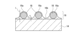
帯電ロール10は、軸体12と、軸体12の外周に形成された弾性体層14と、弾性体層14の外周に形成された表層16と、を備える。表層16は、帯電ロール10の表面に現れる層である。表層16は、バインダーおよび粗さ形成用粒子18を含有する。
The
バインダーは、表層16の主材料であり、ポリアミド(ナイロン)系、アクリル系、ウレタン系、シリコーン系、フッ素系のポリマーを挙げることができる。これらのポリマーは、変性されたものであっても良い。変性基としては、例えば、N−メトキシメチル基、シリコーン基、フッ素基などを挙げることができる。
The binder is a main material of the
バインダーは、水溶性、水分散性、あるいは、水/アルコール混合溶媒可溶性であることが好ましい。バインダーが水溶性、水分散性、あるいは、水/アルコール混合溶媒可溶性であると、粗さ形成用粒子18との水素結合の作用が大きくなるため、耐久時に表層16から粗さ形成用粒子18が脱落するのを抑える効果が向上する。水溶性、水分散性、あるいは、水/アルコール混合溶媒可溶性である、とは、水系塗料のポリマー成分として使用できるポリマーであり、水系塗料において10質量%以上の濃度で使用できるポリマーである。水系塗料は、塗料の助要素の主成分が水である塗料の総称である。水系塗料は、水溶性樹脂系、エマルジョン系に分けられる。水に溶けている樹脂および水にコロイド状に分散している塗料とエマルジョン塗料を含めて水性塗料という。水溶性ポリマーは、固形分濃度10質量%以上で水に溶解するポリマーである。水分散性ポリマーは、固形分濃度10質量%以上で乳化剤を用いて水に分散するポリマーである。水/アルコール混合溶媒可溶性ポリマーは、固形分濃度10質量%以上で水/アルコール混合溶媒に溶解するポリマーである。水/アルコール混合溶媒のアルコールは、低炭素数(低級)の親水性アルコールであり、メタノール、エタノール、プロパノールが挙げられる。水溶性ポリマー、水分散性ポリマー、水/アルコール混合溶媒可溶性ポリマーの固形分濃度の上限は、30質量%程度とされる。
The binder is preferably water-soluble, water-dispersible, or water / alcohol mixed solvent soluble. If the binder is water-soluble, water-dispersible, or soluble in a water / alcohol mixed solvent, the action of hydrogen bonding with the
粗さ形成用粒子18は、表層16の表面に粗さを付与するための粒子である。つまり、表層16の表面に凹凸を付与するための粒子である。表層16の粗さ形成用粒子18が存在している部分が凸部16aとなり、表層16の粗さ形成用粒子18が存在していない部分が凹部16bとなる。表層16の凸部16aは、表層16の凹部16bよりも径方向外側に突出する。表面凹凸は、感光体と帯電ロール10との間における放電空間を増加させ、放電を促す。これにより、帯電性を向上させ、横スジやムラなどの画像不具合を抑えることができる。
The
粗さ形成用粒子18の平均粒子径は、5〜50μmの範囲内である。粗さ形成用粒子18の平均粒子径が5μm未満であると、表層16の表面粗さを十分に確保することができず、電源電圧が低いと、感光体と帯電ロール10の間での放電量が不足し、不要なトナーが印字されて横スジやムラなどの画像不具合が発生する。しかし、粗さ形成用粒子18の平均粒子径が5μm以上であると、耐久時に表層16から粗さ形成用粒子18が脱落しやすい。表層16から粗さ形成用粒子18が脱落すると、放電空間の縮小や抵抗のばらつきが発生し、均一な帯電ができなくなる。
The average particle diameter of the
粗さ形成用粒子18の脱落は、感光体と帯電ロール10の摺擦などによって発生する。そこで、本発明においては、粗さ形成用粒子18を特定の多孔質シリカ粒子で構成することにより、平均粒子径5μm以上の粗さ形成用粒子18を含有する場合においても、耐久時に表層16から粗さ形成用粒子18が脱落するのを抑えることができるようにしている。
The loss of the
特定の多孔質シリカ粒子は、吸油量200〜500ml/100g、孔サイズ5〜20nmの多孔質シリカ粒子である。これにより、バインダーが粗さ形成用粒子18の内部に入り込み、表層16のバインダーと粗さ形成用粒子18の密着性が向上し、平均粒子径5μm以上の比較的大きい粗さ形成用粒子18を用いたときにも耐久時に表層16から粗さ形成用粒子18が脱落するのを抑えることができる。多孔質シリカ粒子の吸油量が200ml/100g未満であると、その内部に入り込むバインダーの量が少なく、バインダーと粗さ形成用粒子18の密着性が不十分となり、耐久時に表層16から粗さ形成用粒子18が脱落しやすい。また、この観点から、多孔質シリカ粒子の吸油量は、より好ましくは250ml/100g以上、さらに好ましくは300ml/100g以上である。多孔質シリカ粒子の孔サイズが5nm未満であると、その内部にバインダーが入り込みにくく、バインダーと粗さ形成用粒子18の密着性が不十分となり、耐久時に表層16から粗さ形成用粒子18が脱落しやすい。また、この観点から、多孔質シリカ粒子の孔サイズは、より好ましくは7nm以上、さらに好ましくは8nm以上である。一方、多孔質シリカ粒子の孔サイズが20nm超であると、多孔質シリカ粒子が凝集しやすくなって分散性が低下し、表面凹凸の均一性が低下する。また、この観点から、多孔質シリカ粒子の孔サイズは、より好ましくは17nm以下、さらに好ましくは15nm以下である。多孔質シリカ粒子の吸油量は、JIS K5101−13−2<顔料試験法−第13部:吸油量−第2節:煮あまに油法>により測定される。多孔質シリカ粒子の孔サイズは、BJH法、水銀圧入法により測定される。
The specific porous silica particles are porous silica particles having an oil absorption of 200 to 500 ml / 100 g and a pore size of 5 to 20 nm. Thereby, the binder enters the inside of the
なお、本発明においても、粗さ形成用粒子18の平均粒子径が50μm超であると、耐久時に表層16から粗さ形成用粒子18が脱落することが抑えられない。したがって、粗さ形成用粒子18の平均粒子径は、50μm以下とする。粗さ形成用粒子18の平均粒子径は、より好ましくは15〜40μmである。平均粒子径が15〜40μmであると、画像不具合を抑える効果と耐久時に表層16から粗さ形成用粒子18が脱落するのを抑える効果のバランスに優れる。粗さ形成用粒子18の平均粒子径は、レーザ回折式粒度分布測定装置を用い、メジアン径により算出する。
Also in the present invention, when the average particle diameter of the
多孔質シリカ粒子は、親水性であると、水溶性、水分散性、あるいは、水/アルコール混合溶媒可溶性のバインダーとの親和性に優れる。そうすると、多孔質シリカ粒子の内部にこのようなバインダーが入り込みやすくなり、バインダーと粗さ形成用粒子18の密着性が向上する。したがって、バインダーが水溶性、水分散性、あるいは、水/アルコール混合溶媒可溶性であるときには、多孔質シリカ粒子は、親水性であることが好ましい。多孔質シリカ粒子の表面のシラノール基は親水性を向上させる。親水性の多孔質シリカ粒子は、表面にシラノール基が多い。一方、親油性の多孔質シリカ粒子は、表面のシラノール基が他の親油性の修飾基(ODS、シリコーンなど)により改質された(表面処理された)ものである。親水性の多孔質シリカ粒子としては、例えばシラノール基を4000μmol/g以上有するものなどが挙げられる。シラノール基の量は、簡便な強熱減量による方法で測定することができる。
When the porous silica particles are hydrophilic, they are excellent in affinity with water-soluble, water-dispersible, or water / alcohol mixed solvent-soluble binders. If it does so, it will become easy to enter such a binder inside the porous silica particle, and the adhesiveness of the binder and the
表層16において、バインダーは、図2に示すように、表層16における粗さ形成用粒子18が存在している部分(凸部16a)から粗さ形成用粒子18が存在していない部分(凹部16b)にかけて裾が広がるように粗さ形成用粒子18の周囲を覆っていることが好ましい。これにより、表層16のバインダーと粗さ形成用粒子18の密着性が向上し、平均粒子径5μm以上の比較的大きい粗さ形成用粒子18を用いたときにも耐久時に表層16から粗さ形成用粒子18が脱落するのを抑えることができる。裾が広がる形状か否かは、凸部16aの最大径の位置から帯電ロール10の径方向に接線lを引いたときに、粗さ形成用粒子18の周囲を覆っているバインダーの表面位置がその接線lよりも内側に入り込んでいるか否かによって判断することができる。例えば図3に示すように、凸部16aの最大径の位置から接線lを引いたときに、粗さ形成用粒子18の周囲を覆っているバインダーの表面位置がその接線lよりも内側に入り込んでいると、その接線lよりも内側に空隙sが形成され、バインダーが充填されていない部分となる。このような空隙sは、バインダーによる粗さ形成用粒子18の保持力を低下させる。裾が広がる形状であると、このような空隙sが形成されず、バインダーによる粗さ形成用粒子18の保持力(密着力)が向上する。このような構造は、表層16を形成するための材料組成物の粘度、塗工液の固形分濃度、乾燥速度等を調整することにより得ることができる。
In the
表層16の厚みは、粗さ形成用粒子18の平均粒子径の1/3以下であることが好ましい。これにより、表面凹凸が大きくなり、感光体と帯電ロール10との間における放電空間を大きくすることができる。そして、放電を促し、帯電性を向上させ、横スジやムラなどの画像不具合を抑えることができる。また、この観点から、表層16の厚みは、より好ましくは粗さ形成用粒子18の平均粒子径の1/4以下、さらに好ましくは粗さ形成用粒子18の平均粒子径の1/5以下である。また、表層16の厚みは、粗さ形成用粒子18の平均粒子径の1/10以上であることが好ましい。これにより、粗さ形成用粒子18の保持力が向上し、耐久時に表層16から粗さ形成用粒子18が脱落するのを抑える効果に優れる。また、この観点から、表層16の厚みは、より好ましくは粗さ形成用粒子18の平均粒子径の1/9以上、さらに好ましくは粗さ形成用粒子18の平均粒子径の1/8以上である。そして、表層16の厚みが粗さ形成用粒子18の平均粒子径の1/10〜1/3の範囲内であると、横スジやムラなどの画像不具合を抑える効果と耐久時に表層16から粗さ形成用粒子18が脱落するのを抑える効果のバランスに優れる。表層16の厚みは、図2に示すように、粗さ形成用粒子18が存在していない部分(凹部16b)における厚みtである。
The thickness of the
粗さ形成用粒子18の含有量は、特に限定されるものではないが、感光体と帯電ロール10との間における放電空間を十分に形成しやすいなどの観点から、バインダー100質量部に対し、5質量部以上であることが好ましい。より好ましくは10質量部以上、さらに好ましくは20質量部以上である。また、表面の凹部にトナーやトナー外添剤が堆積することによる局所的な帯電ムラを抑えやすいなどの観点から、バインダー100質量部に対し、90質量部以下であることが好ましい。より好ましくは80質量部以下、さらに好ましくは70質量部以下である。
The content of the
表層16には、導電性付与のため、カーボンブラック、グラファイト、c−TiO2、c−ZnO、c−SnO2(c−は、導電性を意味する。)、イオン導電剤(4級アンモニウム塩、ホウ酸塩、界面活性剤など)などの従来より公知の導電剤を適宜添加することができる。このうち、酸化スズ(c−SnO2)は、比較的大きい粒子径であるため、多孔質シリカ粒子の孔に充填されにくい。したがって、表層16のバインダーと粗さ形成用粒子18の密着性の向上を妨げにくい。また、酸化スズは、導電性粒子として機能する。この際、多孔質シリカ粒子の孔に充填されないので、最少添加量で抵抗制御を行うことができる。また、必要に応じて、各種添加剤を適宜添加しても良い。添加剤としては、滑剤、加硫促進剤、老化防止剤、光安定剤、粘度調整剤、加工助剤、難燃剤、可塑剤、発泡剤、充填剤、分散剤、消泡剤、顔料、離型剤などを挙げることができる。
The
表層16の表面粗さ(Rz)は、特に限定されるものではないが、感光体と帯電ロール10との間における放電空間を十分に形成しやすいなどの観点から、10μm以上であることが好ましい。より好ましくは15μm以上、さらに好ましくは20μm以上、特に好ましくは25μm以上である。また、耐久時に表層16から粗さ形成用粒子18が脱落するのを抑えやすいなどの観点から、90μm以下であることが好ましい。より好ましくは70μm以下、さらに好ましくは50μm以下、特に好ましくは40μm以下である。表層16の表面粗さ(Rz)は、十点平均粗さであり、JIS B0601(1994)に準拠して測定される。表層16の表面粗さ(Rz)は、粗さ形成用粒子18の粒子径、配合量、バインダー量などにより調整することができる。
The surface roughness (Rz) of the
表層16の体積抵抗率は、好ましくは、104〜109Ω・cm、より好ましくは、105〜108Ω・cm、さらに好ましくは、106〜107Ω・cmの範囲内である。
The volume resistivity of the
軸体12は、導電性を有するものであれば特に限定されない。具体的には、鉄、ステンレス、アルミニウムなどの金属製の中実体、中空体からなる芯金などを例示することができる。軸体12の表面には、必要に応じて、接着剤、プライマーなどを塗布しても良い。つまり、弾性体層14は、接着剤層(プライマー層)を介して軸体12に接着されていてもよい。接着剤、プライマーなどには、必要に応じて導電化を行なっても良い。
The
弾性体層14は、架橋ゴムを含有する。弾性体層14は、未架橋ゴムを含有する導電性ゴム組成物により形成される。架橋ゴムは、未架橋ゴムを架橋することにより得られる。未架橋ゴムは、極性ゴムであってもよいし、非極性ゴムであってもよい。導電性に優れるなどの観点から、未架橋ゴムは極性ゴムが好ましい。
The
極性ゴムは、極性基を有するゴムであり、極性基としては、クロロ基、ニトリル基、カルボキシル基、エポキシ基などを挙げることができる。極性ゴムとしては、具体的には、ヒドリンゴム、ニトリルゴム(NBR)、ウレタンゴム(U)、アクリルゴム(アクリル酸エステルと2−クロロエチルビニルエーテルとの共重合体、ACM)、クロロプレンゴム(CR)、エポキシ化天然ゴム(ENR)などを挙げることができる。極性ゴムのうちでは、体積抵抗率が特に低くなりやすいなどの観点から、ヒドリンゴム、ニトリルゴム(NBR)が好ましい。 The polar rubber is a rubber having a polar group, and examples of the polar group include a chloro group, a nitrile group, a carboxyl group, and an epoxy group. Specific examples of polar rubbers include hydrin rubber, nitrile rubber (NBR), urethane rubber (U), acrylic rubber (a copolymer of acrylic ester and 2-chloroethyl vinyl ether, ACM), and chloroprene rubber (CR). And epoxidized natural rubber (ENR). Among polar rubbers, hydrin rubber and nitrile rubber (NBR) are preferable from the viewpoint of particularly low volume resistivity.
ヒドリンゴムとしては、エピクロルヒドリンの単独重合体(CO)、エピクロルヒドリン−エチレンオキサイド二元共重合体(ECO)、エピクロルヒドリン−アリルグリシジルエーテル二元共重合体(GCO)、エピクロルヒドリン−エチレンオキサイド−アリルグリシジルエーテル三元共重合体(GECO)などを挙げることができる。 Examples of hydrin rubber include epichlorohydrin homopolymer (CO), epichlorohydrin-ethylene oxide binary copolymer (ECO), epichlorohydrin-allyl glycidyl ether binary copolymer (GCO), epichlorohydrin-ethylene oxide-allyl glycidyl ether ternary. A copolymer (GECO) etc. can be mentioned.
ウレタンゴムとしては、分子内にエーテル結合を有するポリエーテル型のウレタンゴムを挙げることができる。ポリエーテル型のウレタンゴムは、両末端にヒドロキシル基を有するポリエーテルとジイソシアネートとの反応により製造できる。ポリエーテルとしては、特に限定されるものではないが、ポリエチレングリコール、ポリプロピレングリコールなどを挙げることができる。ジイソシアネートとしては、特に限定されるものではないが、トリレンジイソシアネート、ジフェニルメタンジイソシアネートなどを挙げることができる。 Examples of the urethane rubber include polyether type urethane rubber having an ether bond in the molecule. A polyether type urethane rubber can be produced by a reaction between a polyether having hydroxyl groups at both ends and a diisocyanate. The polyether is not particularly limited, and examples thereof include polyethylene glycol and polypropylene glycol. Although it does not specifically limit as diisocyanate, Tolylene diisocyanate, diphenylmethane diisocyanate, etc. can be mentioned.
架橋剤としては、硫黄架橋剤、過酸化物架橋剤、脱塩素架橋剤を挙げることができる。これらの架橋剤は、単独で用いても良いし、2種以上組み合わせて用いても良い。 Examples of the crosslinking agent include a sulfur crosslinking agent, a peroxide crosslinking agent, and a dechlorination crosslinking agent. These crosslinking agents may be used alone or in combination of two or more.
硫黄架橋剤としては、粉末硫黄、沈降硫黄、コロイド硫黄、表面処理硫黄、不溶性硫黄、塩化硫黄、チウラム系加硫促進剤、高分子多硫化物などの従来より公知の硫黄架橋剤を挙げることができる。 Examples of the sulfur crosslinking agent include conventionally known sulfur crosslinking agents such as powdered sulfur, precipitated sulfur, colloidal sulfur, surface-treated sulfur, insoluble sulfur, sulfur chloride, thiuram vulcanization accelerator, and polymer polysulfide. it can.
過酸化物架橋剤としては、パーオキシケタール、ジアルキルパーオキサイド、パーオキシエステル、ケトンパーオキサイド、パーオキシジカーボネート、ジアシルパーオキサイド、ハイドロパーオキサイドなどの従来より公知の過酸化物架橋剤を挙げることができる。 Examples of peroxide crosslinking agents include conventionally known peroxide crosslinking agents such as peroxyketals, dialkyl peroxides, peroxyesters, ketone peroxides, peroxydicarbonates, diacyl peroxides and hydroperoxides. Can do.
脱塩素架橋剤としては、ジチオカーボネート化合物を挙げることができる。より具体的には、キノキサリン−2,3−ジチオカーボネート、6−メチルキノキサリン−2,3−ジチオカーボネート、6−イソプロピルキノキサリン−2,3−ジチオカーボネート、5,8−ジメチルキノキサリン−2,3−ジチオカーボネートなどを挙げることができる。 Examples of the dechlorination crosslinking agent include dithiocarbonate compounds. More specifically, quinoxaline-2,3-dithiocarbonate, 6-methylquinoxaline-2,3-dithiocarbonate, 6-isopropylquinoxaline-2,3-dithiocarbonate, 5,8-dimethylquinoxaline-2,3- A dithiocarbonate etc. can be mentioned.
架橋剤の配合量としては、ブリードしにくいなどの観点から、未架橋ゴム100質量部に対して、好ましくは0.1〜2質量部の範囲内、より好ましくは0.3〜1.8質量部の範囲内、さらに好ましくは0.5〜1.5質量部の範囲内である。 The blending amount of the crosslinking agent is preferably within a range of 0.1 to 2 parts by mass, more preferably 0.3 to 1.8 parts by mass with respect to 100 parts by mass of the uncrosslinked rubber from the viewpoint of difficulty in bleeding. In the range of parts, more preferably in the range of 0.5 to 1.5 parts by weight.
架橋剤として脱塩素架橋剤を用いる場合には、脱塩素架橋促進剤を併用しても良い。脱塩素架橋促進剤としては、1,8−ジアザビシクロ(5,4,0)ウンデセン−7(以下、DBUと略称する。)もしくはその弱酸塩を挙げることができる。脱塩素架橋促進剤は、DBUの形態として用いても良いが、その取り扱い面から、その弱酸塩の形態として用いることが好ましい。DBUの弱酸塩としては、炭酸塩、ステアリン酸塩、2−エチルヘキシル酸塩、安息香酸塩、サリチル酸塩、3−ヒドロキシ−2−ナフトエ酸塩、フェノール樹脂塩、2−メルカプトベンゾチアゾール塩、2−メルカプトベンズイミダゾール塩などを挙げることができる。 When a dechlorination crosslinking agent is used as the crosslinking agent, a dechlorination crosslinking accelerator may be used in combination. Examples of the dechlorination crosslinking accelerator include 1,8-diazabicyclo (5,4,0) undecene-7 (hereinafter abbreviated as DBU) or a weak acid salt thereof. Although the dechlorination crosslinking accelerator may be used in the form of DBU, it is preferably used in the form of its weak acid salt from the viewpoint of handling. Examples of weak acid salts of DBU include carbonate, stearate, 2-ethylhexylate, benzoate, salicylate, 3-hydroxy-2-naphthoate, phenol resin salt, 2-mercaptobenzothiazole salt, 2- Examples include mercaptobenzimidazole salts.
脱塩素架橋促進剤の含有量としては、ブリードしにくいなどの観点から、未架橋ゴム100質量部に対して、0.1〜2質量部の範囲内であることが好ましい。より好ましくは0.3〜1.8質量部の範囲内、さらに好ましくは0.5〜1.5質量部の範囲内である。 The content of the dechlorination crosslinking accelerator is preferably in the range of 0.1 to 2 parts by mass with respect to 100 parts by mass of the uncrosslinked rubber from the viewpoint of difficulty in bleeding. More preferably, it is in the range of 0.3 to 1.8 parts by mass, and still more preferably in the range of 0.5 to 1.5 parts by mass.
弾性体層14には、導電性付与のため、カーボンブラック、グラファイト、c−TiO2、c−ZnO、c−SnO2(c−は、導電性を意味する。)、イオン導電剤(4級アンモニウム塩、ホウ酸塩、界面活性剤など)などの従来より公知の導電剤を適宜添加することができる。また、必要に応じて、各種添加剤を適宜添加しても良い。添加剤としては、滑剤、加硫促進剤、老化防止剤、光安定剤、粘度調整剤、加工助剤、難燃剤、可塑剤、発泡剤、充填剤、分散剤、消泡剤、顔料、離型剤などを挙げることができる。
The
弾性体層14は、架橋ゴムの種類、イオン導電剤の配合量、電子導電剤の配合などにより、所定の体積抵抗率に調整することができる。弾性体層14の体積抵抗率は、用途などに応じて102〜1010Ω・cm、103〜109Ω・cm、104〜108Ω・cmの範囲などに適宜設定すればよい。
The
弾性体層14の厚みは、特に限定されるものではなく、用途などに応じて0.1〜10mmの範囲内などで適宜設定すればよい。
The thickness of the
導電性ロール10は、例えば、次のようにして製造することができる。まず、軸体12をロール成形金型の中空部に同軸的に設置し、未架橋の導電性ゴム組成物を注入して、加熱・硬化(架橋)させた後、脱型するか、あるいは、軸体12の表面に未架橋の導電性ゴム組成物を押出成形するなどにより、軸体12の外周に弾性体層14を形成する。次いで、形成した弾性体層14の外周に表層形成用組成物を塗工し、必要に応じて紫外線照射や熱処理などの架橋処理を行うことにより、表層16を形成する。これにより、導電性ロール10を製造できる。塗工方法としては、ロールコーティング法や、ディッピング法、スプレーコート法などの各種コーティング法を適用することができる。表層16を塗工により形成できると、表層16を薄く均一に形成できるため、均一な表面抵抗が得られやすい。
The
以上の構成の帯電ロール10によれば、平均粒子径5〜50μmの比較的大きい粒子を粗さ形成用粒子18として表層16に含有させているので、感光体と帯電ロール10との間における放電空間を増加させて、放電を促すことができる。これにより、帯電性を向上させ、横スジやムラなどの画像不具合を抑えることができる。そして、粗さ形成用粒子18が多孔質シリカ粒子で構成されており、当該多孔質シリカ粒子が、吸油量200〜500ml/100g、孔サイズ5〜20nmであることにより、バインダーが粗さ形成用粒子18の内部に入り込み、表層16のバインダーと粗さ形成用粒子18の密着性が向上し、平均粒子径5〜50μmの比較的大きい粗さ形成用粒子18を用いたときにも耐久時に表層16から粗さ形成用粒子18が脱落するのを抑えることができる。
According to the charging
本発明に係る導電性ロールの構成としては、図1に示す構成に限定されるものではない。例えば、図1に示す導電性ロール10において、軸体12と弾性体層14との間に他の弾性体層を備えた構成であってもよい。この場合、他の弾性体層は、導電性ロールのベースとなる層であり、弾性体層14が導電性ロールの抵抗調整を行う抵抗調整層などとして機能する。他の弾性体層は、例えば、弾性体層14を構成する材料として挙げられた材料のいずれかにより構成することができる。
The configuration of the conductive roll according to the present invention is not limited to the configuration shown in FIG. For example, the
また、図1に示す導電性ロール10において、弾性体層14と表層16との間に他の弾性体層を備えた構成であってもよい。この場合、弾性体層14は、導電性ロールのベースとなる層であり、他の弾性体層が導電性ロールの抵抗調整を行う抵抗調整層などとして機能する。他の弾性体層は、例えば、弾性体層14を構成する材料として挙げられた材料のいずれかにより構成することができる。
Further, the
以下、実施例および比較例を用いて本発明を詳細に説明する。 Hereinafter, the present invention will be described in detail using Examples and Comparative Examples.
(実施例1)
<導電性ゴム組成物の調製>
ヒドリンゴム(ECO、日本ゼオン社製、「HydrinT3106」)100質量部に対し、イオン導電剤(テトラn−ブチルアンモニウムパークロレート、n−Bu4N・ClO4)を3質量部、架橋剤として硫黄(鶴見化学社製、「イオウ−PTC」)を2質量部添加し、これらを攪拌機により撹拌、混合して導電性ゴム組成物を調製した。
Example 1
<Preparation of conductive rubber composition>
For 100 parts by mass of hydrin rubber (ECO, manufactured by Nippon Zeon Co., Ltd., “Hydrin T3106”), 3 parts by mass of ionic conductive agent (tetra-n-butylammonium perchlorate, n-Bu 4 N · ClO 4 ), sulfur as a crosslinking agent ( 2 parts by mass of “Sulfur-PTC” manufactured by Tsurumi Chemical Co., Ltd.) was added, and these were stirred and mixed with a stirrer to prepare a conductive rubber composition.
<表層形成用組成物の調製>
バインダーとしてナイロン塗料(固形分として100質量部)と、多孔質シリカ粒子30質量部と、導電性酸化スズ60質量部と、を混合して、表層形成用組成物を調製した。バインダーの固形分濃度は10質量%である。
<Preparation of surface layer forming composition>
Nylon paint (100 parts by mass as a solid content) as a binder, 30 parts by mass of porous silica particles, and 60 parts by mass of conductive tin oxide were mixed to prepare a surface layer forming composition. The solid content concentration of the binder is 10% by mass.
<帯電ロールの作製>
成形金型に芯金(軸体、直径8mm)をセットし、上記の導電性ゴム組成物を注入し、170℃で30分加熱した後、冷却、脱型して、芯金の外周に厚み1.5mmの弾性体層を形成した。次いで、上記の表層形成用組成物を弾性体層の外周面にロールコートし、120℃で50分加熱して、弾性体層の外周に表層(凹部における厚みt=5μm、多孔質シリカ粒子の平均粒子径r(μm)との比t/r=1/6)を形成した。以上により、帯電ロールを作製した。
<Preparation of charging roll>
Set the core metal (shaft body, diameter 8 mm) in the molding die, inject the conductive rubber composition described above, heat at 170 ° C. for 30 minutes, cool and demold, and thicken the outer periphery of the core metal A 1.5 mm elastic layer was formed. Next, the surface layer forming composition is roll-coated on the outer peripheral surface of the elastic layer, heated at 120 ° C. for 50 minutes, and the outer layer of the elastic layer (thickness t = 5 μm in the recess, porous silica particles) A ratio t / r = 1/6) with an average particle diameter r (μm) was formed. Thus, a charging roll was produced.
(実施例2、4〜10、比較例1〜6)
表1に記載のバインダー固形分濃度とし、表1に記載の多孔質シリカ粒子を用いた以外は実施例1と同様にして、帯電ロールを作製した。
(Examples 2, 4 to 10, Comparative Examples 1 to 6)
A charging roll was produced in the same manner as in Example 1 except that the binder solid content concentration shown in Table 1 was used and the porous silica particles shown in Table 1 were used.
(実施例3)
表層形成用組成物において、導電性酸化スズを配合しなかった以外は実施例2と同様にして帯電ロールを作製した。
(Example 3)
A charging roll was produced in the same manner as in Example 2 except that the surface tin forming composition did not contain conductive tin oxide.
使用した各成分は、以下の通りである。
・ナイロン塗料:固形分:N−メトキシメチル化6−ナイロン、溶媒:メタノール、ナガセケムテックス社製、「トレジンF−30K」、SP値:10.91
・多孔質シリカ粒子:AGCエスアイテック製「サンスフェア」(親水性)
Each component used is as follows.
Nylon paint: solid content: N-methoxymethylated 6-nylon, solvent: methanol, manufactured by Nagase ChemteX Corporation, “Tresin F-30K”, SP value: 10.91
-Porous silica particles: "Sunsphere" (hydrophilic) manufactured by AGC S-Itech
作製した各帯電ロールについて、画像不具合(初期画像評価)、粒子脱落(耐久時画像評価)の評価をした。評価方法および評価基準は以下の通りである。評価結果および表層形成用組成物の配合組成(質量部)を表に示す。 Each charging roll produced was evaluated for image defects (initial image evaluation) and particle dropout (durability image evaluation). Evaluation methods and evaluation criteria are as follows. The evaluation results and the composition (parts by mass) of the composition for forming the surface layer are shown in the table.
(画像評価(初期))
各帯電ロールをカラーレーザープリンター(リコー社製、「IPSIO SP C310」)に取り付け、所定の画像(600dpiドットパターン:ハーフトーン画像)を出力した。その後、出力された画像を目視で観察し、画像評価を行った。出力された初期画像に、画像スジが認められなかった場合を、初期の帯電性に特に優れるとして「A+」とした。また、画像スジはやや認められたものの、実使用上影響がないレベルであった場合を、初期の帯電性に優れるとして「A+」とした。さらに、画像スジが認められ、実使用上影響があるレベルであった場合を、初期の帯電性に劣るとして「B」とした。なお、本評価は、粗さ形成用粒子が保持されている初期の段階であっても、粗さ形成用粒子による放電空間が不十分である場合には、帯電性に劣り、画像スジが発生することがあることを確認するための試験である。
(Image evaluation (initial))
Each charging roll was attached to a color laser printer (“IPSIO SP C310” manufactured by Ricoh Company), and a predetermined image (600 dpi dot pattern: halftone image) was output. Thereafter, the output image was visually observed and image evaluation was performed. In the case where no image streak was observed in the output initial image, “A +” was designated as being particularly excellent in initial chargeability. In addition, although image streaks were somewhat recognized, the case where the image streak was at a level that did not affect actual use was designated as “A +” as being excellent in the initial chargeability. Furthermore, when the image streak was recognized and the actual use level was affected, “B” was assigned as inferior initial chargeability. In this evaluation, even in the initial stage where the roughness forming particles are held, if the discharge space by the roughness forming particles is insufficient, the charging property is inferior and image streaks are generated. It is a test to confirm that there is something to do.
(画像評価(耐久後))
各帯電ロールをカラーレーザープリンター(リコー社製、「IPSIO SP C310」)に取り付け、15℃×10%RH環境下にて10,000枚の印字テストを行った。なお、印字テストでは、シアントナーを使用し、印字率は5%チャートであった。印字テストの後、上記プリンターから帯電ロールを取り外し、帯電ロールに付着しているトナーおよび外添剤を拭き取った。その後、帯電ロールを再び上記プリンターに取り付け、所定の画像(600dpiドットパターン:ハーフトーン画像)を出力した。出力された画像を目視で観察するとともに、さらに、帯電ロールを取り出し、表層表面を走査型電子顕微鏡にて観察した。表層表面に粗さ形成用粒子の脱落跡が確認されず、画像スジが認められなかった場合を、特に長期にわたって画質を維持しているとして「A+」とした。表層表面に粗さ形成用粒子の脱落跡が確認されず、画像スジはやや認められたものの、実使用上影響がないレベルであった場合を、長期にわたって画質を維持しているとして「A」とした。表層表面に粗さ形成用粒子の脱落跡が確認されなかったものの、画像スジが認められ、実使用上影響があるレベルであった場合を「B」とした。表層表面に粗さ形成用粒子の脱落跡が確認され、画像スジが認められた場合を「C」とした。
(Image evaluation (after endurance))
Each charging roll was attached to a color laser printer (“IPSIO SP C310” manufactured by Ricoh Co., Ltd.), and a printing test on 10,000 sheets was performed in a 15 ° C. × 10% RH environment. In the printing test, cyan toner was used, and the printing rate was a 5% chart. After the printing test, the charging roll was removed from the printer, and the toner and external additives adhering to the charging roll were wiped off. Thereafter, the charging roll was attached to the printer again, and a predetermined image (600 dpi dot pattern: halftone image) was output. While visually observing the output image, the charging roll was taken out and the surface of the surface layer was observed with a scanning electron microscope. A case where no drop of roughness forming particles was observed on the surface of the surface layer and no image streak was observed was designated as “A +” because the image quality was maintained particularly for a long period of time. “A” indicates that the image quality is maintained over a long period of time when there is no trace of roughness-forming particles on the surface and the image streaks are somewhat recognized but there is no effect on actual use. It was. Although no trace of roughness-forming particles was observed on the surface of the surface layer, image streaks were observed, and the case where the level was influential in actual use was designated as “B”. “C” was defined as the case where roughness marks were observed on the surface of the surface layer, and image streaks were observed.

比較例1、2では、表層に配合している多孔質シリカ粒子の平均粒子径が小さすぎるため、表面凹凸が小さく、初期から画像不具合が生じている。比較例3,4,5,6では、表層に配合している多孔質シリカ粒子の吸油量が少ないため、バインダーが多孔質シリカ粒子に十分入り込んでおらず、多孔質シリカ粒子の保持力が弱く、耐久時に粒子の脱離が生じて、耐久時の画像に不具合が生じている。これに対し、実施例では、表層が、バインダー、特定の多孔質シリカ粒子を含有しており、耐久時にも表層から粒子が脱落するのが抑えられ、初期および耐久時において画像不具合が抑えられている。 In Comparative Examples 1 and 2, since the average particle diameter of the porous silica particles blended in the surface layer is too small, the surface unevenness is small, and image defects occur from the beginning. In Comparative Examples 3, 4, 5, and 6, since the amount of oil absorption of the porous silica particles blended in the surface layer is small, the binder does not sufficiently enter the porous silica particles and the holding power of the porous silica particles is weak. The particles are detached at the time of durability, and the image at the time of durability is defective. On the other hand, in the examples, the surface layer contains a binder and specific porous silica particles, and particles are prevented from falling off from the surface layer even during durability, and image defects are suppressed in the initial and durability. Yes.
実施例3および他の実施例との比較から、表層が導電性酸化スズを含有することで、画質が向上することがわかる。実施例4,8および他の実施例との比較から、表層の乾燥速度を早くすると、図2に示すように、バインダーは、表層における粗さ形成用粒子が存在している部分から粗さ形成用粒子が存在していない部分にかけて裾が広がるように粗さ形成用粒子の周囲を覆う構成とすることができ、このような構造によって、図3に示すような空隙sが形成される構造(実施例4,8)よりも耐久後の画像評価に優れ、特に長期にわたって画質を維持できることがわかる。 From a comparison with Example 3 and other Examples, it can be seen that the image quality is improved when the surface layer contains conductive tin oxide. From comparison with Examples 4 and 8 and other examples, when the drying speed of the surface layer is increased, as shown in FIG. 2, the binder forms roughness from the portion where the particles for roughness formation in the surface layer exist. 3 may be configured to cover the periphery of the roughness forming particles so that the skirt spreads over a portion where the particles do not exist, and such a structure forms a void s as shown in FIG. It can be seen that the image evaluation after endurance is superior to those of Examples 4 and 8), and the image quality can be maintained particularly for a long period of time.
以上、本発明の実施形態・実施例について説明したが、本発明は上記実施形態・実施例に何ら限定されるものではなく、本発明の趣旨を逸脱しない範囲内で種々の改変が可能である。 Although the embodiments and examples of the present invention have been described above, the present invention is not limited to the above-described embodiments and examples, and various modifications can be made without departing from the spirit of the present invention. .
10 帯電ロール
12 軸体
14 弾性体層
16 表層
18 粗さ形成用粒子
DESCRIPTION OF
Claims (7)
前記表層が、バインダーおよび粗さ形成用粒子を含有し、前記粗さ形成用粒子が存在している部分において前記粗さ形成用粒子が存在していない部分よりも径方向外側に突出する凸部を有しており、
前記粗さ形成用粒子が、多孔質シリカ粒子で構成されており、当該多孔質シリカ粒子は、平均粒子径5〜50μm、吸油量200〜500ml/100g、孔サイズ5〜20nmであり、
前記多孔質シリカ粒子が、親水性であることを特徴とする電子写真機器用帯電ロール。 A shaft body, an elastic body layer formed on the outer periphery of the shaft body, and a surface layer formed on the outer periphery of the elastic body layer,
The surface layer contains a binder and roughness-forming particles, and protrudes radially outward from a portion where the roughness-forming particles are not present in a portion where the roughness-forming particles are present. Have
Wherein the roughness-forming particles are composed of porous silica particles, the porous silica particles have an average particle diameter of 5 to 50 [mu] m, oil absorption 200-500 ml / 100 g, Ri pore size 5~20nm der,
The porous silica particles, the charging roller for electrophotographic apparatus, wherein the hydrophilic der Rukoto.
前記表層が、バインダーおよび粗さ形成用粒子を含有し、前記粗さ形成用粒子が存在している部分において前記粗さ形成用粒子が存在していない部分よりも径方向外側に突出する凸部を有しており、
前記粗さ形成用粒子が、多孔質シリカ粒子で構成されており、当該多孔質シリカ粒子は、平均粒子径5〜50μm、吸油量200〜500ml/100g、孔サイズ5〜20nmであり、
前記バインダーは、前記表層における粗さ形成用粒子が存在している部分から粗さ形成用粒子が存在していない部分にかけて裾が広がるように前記粗さ形成用粒子の周囲を覆っていることを特徴とする電子写真機器用帯電ロール。 A shaft body, an elastic body layer formed on the outer periphery of the shaft body, and a surface layer formed on the outer periphery of the elastic body layer,
The surface layer contains a binder and roughness-forming particles, and protrudes radially outward from a portion where the roughness-forming particles are not present in a portion where the roughness-forming particles are present. Have
The roughness forming particles are composed of porous silica particles, and the porous silica particles have an average particle diameter of 5 to 50 μm, an oil absorption of 200 to 500 ml / 100 g, and a pore size of 5 to 20 nm.
The binder covers the periphery of the roughness forming particles so that the skirt spreads from a portion where the roughness forming particles are present in the surface layer to a portion where the roughness forming particles are not present. charging roll for you that electronic photo equipment and features.
Priority Applications (4)
| Application Number | Priority Date | Filing Date | Title |
|---|---|---|---|
| JP2015213190A JP6155312B2 (en) | 2015-10-29 | 2015-10-29 | Charging roll for electrophotographic equipment |
| PCT/JP2016/078423 WO2017073221A1 (en) | 2015-10-29 | 2016-09-27 | Charging roll for electrographic apparatus |
| CN201680053164.8A CN108027578A (en) | 2015-10-29 | 2016-09-27 | Electrified Roller Used For Electric Camera Device |
| US15/821,765 US9971271B2 (en) | 2015-10-29 | 2017-11-23 | Charging roll for electrographic apparatus |
Applications Claiming Priority (1)
| Application Number | Priority Date | Filing Date | Title |
|---|---|---|---|
| JP2015213190A JP6155312B2 (en) | 2015-10-29 | 2015-10-29 | Charging roll for electrophotographic equipment |
Publications (3)
| Publication Number | Publication Date |
|---|---|
| JP2017083711A JP2017083711A (en) | 2017-05-18 |
| JP6155312B2 true JP6155312B2 (en) | 2017-06-28 |
| JP2017083711A5 JP2017083711A5 (en) | 2017-06-29 |
Family
ID=58630457
Family Applications (1)
| Application Number | Title | Priority Date | Filing Date |
|---|---|---|---|
| JP2015213190A Active JP6155312B2 (en) | 2015-10-29 | 2015-10-29 | Charging roll for electrophotographic equipment |
Country Status (4)
| Country | Link |
|---|---|
| US (1) | US9971271B2 (en) |
| JP (1) | JP6155312B2 (en) |
| CN (1) | CN108027578A (en) |
| WO (1) | WO2017073221A1 (en) |
Families Citing this family (3)
| Publication number | Priority date | Publication date | Assignee | Title |
|---|---|---|---|---|
| WO2018193779A1 (en) | 2017-04-20 | 2018-10-25 | 株式会社ニコン | Article used in contact with living body or biological sample, medical instrument, and artificial joint |
| JP7202540B2 (en) * | 2018-11-29 | 2023-01-12 | 株式会社リコー | image forming device |
| US20240094656A1 (en) * | 2021-02-01 | 2024-03-21 | Nok Corporation | Charging roll |
Family Cites Families (12)
| Publication number | Priority date | Publication date | Assignee | Title |
|---|---|---|---|---|
| JP2003207995A (en) * | 2002-01-16 | 2003-07-25 | Canon Inc | Electrostatic charging roller, image forming device, electrostatic charging method and process cartridge |
| JP2003316113A (en) * | 2002-04-19 | 2003-11-06 | Canon Inc | Electrophotographic device and process cartridge |
| JP4732920B2 (en) * | 2006-02-23 | 2011-07-27 | 東海ゴム工業株式会社 | Charging roll |
| JPWO2010092925A1 (en) * | 2009-02-12 | 2012-08-16 | あすか製薬株式会社 | Solid dispersion, pharmaceutical composition thereof, and production method thereof |
| JP5314568B2 (en) * | 2009-10-30 | 2013-10-16 | 東海ゴム工業株式会社 | Charging roll |
| JP5908699B2 (en) * | 2011-10-31 | 2016-04-26 | 富士フイルム株式会社 | Cosmetics |
| WO2014118832A1 (en) * | 2013-01-29 | 2014-08-07 | キヤノン株式会社 | Electrophotographic process cartridge and electrophotographic apparatus |
| JP5777665B2 (en) * | 2013-01-29 | 2015-09-09 | キヤノン株式会社 | Charging member, process cartridge, and electrophotographic apparatus |
| KR20140103517A (en) * | 2013-02-18 | 2014-08-27 | 삼성전자주식회사 | Toner for developing electrostatic latent images |
| CN105556397B (en) * | 2013-09-20 | 2018-07-10 | 佳能株式会社 | Charging member and its manufacturing method, handle box and electronic photographing device |
| JP6067632B2 (en) | 2013-11-21 | 2017-01-25 | 三星電子株式会社Samsung Electronics Co.,Ltd. | Charging member |
| US9256153B2 (en) * | 2014-04-18 | 2016-02-09 | Canon Kabushiki Kaisha | Charging member, process cartridge and electrophotographic apparatus |
-
2015
- 2015-10-29 JP JP2015213190A patent/JP6155312B2/en active Active
-
2016
- 2016-09-27 WO PCT/JP2016/078423 patent/WO2017073221A1/en active Application Filing
- 2016-09-27 CN CN201680053164.8A patent/CN108027578A/en active Pending
-
2017
- 2017-11-23 US US15/821,765 patent/US9971271B2/en active Active
Also Published As
| Publication number | Publication date |
|---|---|
| JP2017083711A (en) | 2017-05-18 |
| US9971271B2 (en) | 2018-05-15 |
| US20180107134A1 (en) | 2018-04-19 |
| CN108027578A (en) | 2018-05-11 |
| WO2017073221A1 (en) | 2017-05-04 |
Similar Documents
| Publication | Publication Date | Title |
|---|---|---|
| JP6722606B2 (en) | Charging roll for electrophotographic equipment | |
| JP6155416B1 (en) | Charging roll for electrophotographic equipment | |
| JP5612805B2 (en) | Charging roll | |
| JP6155312B2 (en) | Charging roll for electrophotographic equipment | |
| JP2012047871A (en) | Conductive member for electrophotographic apparatus | |
| JP5325511B2 (en) | ELECTROPHOTOGRAPHIC CHARGING ROLL AND ELECTROPHOTOGRAPHIC CHARGING ROLL MANUFACTURING METHOD | |
| CN109923481B (en) | Charging member for electrophotographic apparatus and method for manufacturing charging member for electrophotographic apparatus | |
| US20180231908A1 (en) | Charging roll for electrophotographic apparatus | |
| JP6722613B2 (en) | Charging roll for electrophotographic equipment | |
| JP6850094B2 (en) | Conductive rolls for electrophotographic equipment | |
| JP2017156396A (en) | Charging roll for electrophotographic apparatus | |
| JP2017116685A (en) | Conductive member for electrophotographic apparatus | |
| WO2020158550A1 (en) | Charging roll for electrophotographic equipment | |
| JP2018017943A (en) | Conductive roll for electrophotographic apparatus | |
| WO2022138202A1 (en) | Charging roll for electrophotographic equipment | |
| CN110753883B (en) | Charging member for electrophotographic apparatus | |
| JP6133617B2 (en) | Conductive roller | |
| JP2006010754A (en) | Conductive elastic roll | |
| JP5363012B2 (en) | Charging roll for electrophotographic equipment |
Legal Events
| Date | Code | Title | Description |
|---|---|---|---|
| A521 | Written amendment |
Free format text: JAPANESE INTERMEDIATE CODE: A523 Effective date: 20170424 |
|
| A621 | Written request for application examination |
Free format text: JAPANESE INTERMEDIATE CODE: A621 Effective date: 20170424 |
|
| A871 | Explanation of circumstances concerning accelerated examination |
Free format text: JAPANESE INTERMEDIATE CODE: A871 Effective date: 20170424 |
|
| A975 | Report on accelerated examination |
Free format text: JAPANESE INTERMEDIATE CODE: A971005 Effective date: 20170512 |
|
| TRDD | Decision of grant or rejection written | ||
| A01 | Written decision to grant a patent or to grant a registration (utility model) |
Free format text: JAPANESE INTERMEDIATE CODE: A01 Effective date: 20170530 |
|
| A61 | First payment of annual fees (during grant procedure) |
Free format text: JAPANESE INTERMEDIATE CODE: A61 Effective date: 20170605 |
|
| R150 | Certificate of patent or registration of utility model |
Ref document number: 6155312 Country of ref document: JP Free format text: JAPANESE INTERMEDIATE CODE: R150 |