JP5875264B2 - Method for manufacturing charging member - Google Patents
Method for manufacturing charging member Download PDFInfo
- Publication number
- JP5875264B2 JP5875264B2 JP2011148186A JP2011148186A JP5875264B2 JP 5875264 B2 JP5875264 B2 JP 5875264B2 JP 2011148186 A JP2011148186 A JP 2011148186A JP 2011148186 A JP2011148186 A JP 2011148186A JP 5875264 B2 JP5875264 B2 JP 5875264B2
- Authority
- JP
- Japan
- Prior art keywords
- spherical
- elastic layer
- particles
- layer
- roller
- Prior art date
- Legal status (The legal status is an assumption and is not a legal conclusion. Google has not performed a legal analysis and makes no representation as to the accuracy of the status listed.)
- Active
Links
Images


Classifications
-
- G—PHYSICS
- G03—PHOTOGRAPHY; CINEMATOGRAPHY; ANALOGOUS TECHNIQUES USING WAVES OTHER THAN OPTICAL WAVES; ELECTROGRAPHY; HOLOGRAPHY
- G03G—ELECTROGRAPHY; ELECTROPHOTOGRAPHY; MAGNETOGRAPHY
- G03G15/00—Apparatus for electrographic processes using a charge pattern
- G03G15/02—Apparatus for electrographic processes using a charge pattern for laying down a uniform charge, e.g. for sensitising; Corona discharge devices
- G03G15/0208—Apparatus for electrographic processes using a charge pattern for laying down a uniform charge, e.g. for sensitising; Corona discharge devices by contact, friction or induction, e.g. liquid charging apparatus
- G03G15/0216—Apparatus for electrographic processes using a charge pattern for laying down a uniform charge, e.g. for sensitising; Corona discharge devices by contact, friction or induction, e.g. liquid charging apparatus by bringing a charging member into contact with the member to be charged, e.g. roller, brush chargers
- G03G15/0233—Structure, details of the charging member, e.g. chemical composition, surface properties
Description
本発明は電子写真装置等に用いられる帯電部材およびその製造方法、並びに電子写真装置に関する。 The present invention relates to a charging member used in an electrophotographic apparatus and the like, a manufacturing method thereof, and an electrophotographic apparatus.
電子写真感光体などの被帯電体の接触帯電に用いられる帯電部材には、被帯電体との均一なニップを確保し、被帯電体の傷付き防止のため、ゴムや熱可塑性エラストマー等を含む弾性層が設けられているのが一般的である。しかし、かかる弾性層の表面には、トナーや外添剤が付着し易い。また、長期にわたって弾性層と感光体とが静止状態で当接した場合、弾性層の当接部分に永久変形が生じることがある。かかる課題に対して、特許文献1には、弾性層の表面に紫外線や電子線等のエネルギー線を照射して表面改質層を設けてなる帯電部材が開示されている。 The charging member used for contact charging of a charged body such as an electrophotographic photosensitive member includes rubber, a thermoplastic elastomer or the like to ensure a uniform nip with the charged body and prevent the charged body from being damaged. Generally, an elastic layer is provided. However, toner and external additives are likely to adhere to the surface of the elastic layer. In addition, when the elastic layer and the photoconductor are in contact with each other over a long period of time, permanent deformation may occur in the contact portion of the elastic layer. In order to deal with this problem, Patent Document 1 discloses a charging member in which a surface modification layer is provided by irradiating the surface of an elastic layer with energy rays such as ultraviolet rays and electron beams.
しかしながら、上記特許文献1に係る帯電部材を検討した結果、電子写真感光体にクリーニング不良を生じさせることがあった。電子写真感光体に発生するクリーニング不良とは、本来であれば弾性ブレードによって除去されるべき、電子写真感光体の表面の残留トナーが弾性ブレードをすり抜け、次の電子写真画像形成サイクルによって形成された電子写真画像の品位を低下させる現象をいう。
そこで本発明の目的は、感光体との間で十分なニップ幅を形成し得るだけの柔軟性を有しつつ、電子写真感光体にクリーニング不良を生じさせにくい帯電部材およびその製造方法を提供することにある。また、本発明の他の目的は、経時的な帯電性能の低下が少ないことにより、長期に亘って安定して高品位な電子写真画像を形成することのできる電子写真装置の提供にある。
However, as a result of studying the charging member according to Patent Document 1, cleaning failure may occur in the electrophotographic photosensitive member. The cleaning failure generated in the electrophotographic photosensitive member is formed by the next electrophotographic image forming cycle because the residual toner on the surface of the electrophotographic photosensitive member that should be removed by the elastic blade passes through the elastic blade. A phenomenon that reduces the quality of electrophotographic images.
SUMMARY OF THE INVENTION Accordingly, an object of the present invention is to provide a charging member that is flexible enough to form a sufficient nip width with a photoconductor and hardly causes poor cleaning on the electrophotographic photoconductor, and a method for manufacturing the same. There is. Another object of the present invention is to provide an electrophotographic apparatus capable of forming a high-quality electrophotographic image stably over a long period of time because of a small decrease in charging performance with time.
本発明によれば、
導電性の支持体と、表面層である弾性層とを有し、
該弾性層は、電子線の照射によって硬化された領域を表面に有しており、
該硬化された領域は、球状粒子を該弾性層の表面に露出した状態で支持し、それにより該表面が粗面化されており、
該球状粒子は、球状シリカ粒子、球状アルミナ粒子および球状ジルコニア粒子からなる群から選ばれる少なくとも一つの球状粒子である帯電部材の製造方法であって、
(1)支持体上に、球状シリカ粒子、球状アルミナ粒子および球状ジルコニア粒子からなる群から選ばれる少なくとも一つの球状粒子を含むゴム層を形成する工程と、
(2)該ゴム層の表面を研摩して該球状粒子の一部分を露出させる工程と、
(3)該工程(2)によって得た、該球状粒子の一部分が露出した該ゴム層の表面に電子線を照射することによって、表面を硬化させて、表面部分のみに硬化された領域を有し、該硬化された領域によって、該球状粒子が該弾性層の表面に露出した状態で支持されてなり、かつ、それによって、該表面が粗面化されてなる弾性層を形成する工程と、
を含む帯電部材の製造方法が提供される。
According to the present invention,
It has a conductive support and an elastic layer that is a surface layer,
The elastic layer has a region hardened by electron beam irradiation on the surface,
The cured region supports the spherical particles in a state of being exposed on the surface of the elastic layer, whereby the surface is roughened,
The spherical particles are a method for producing a charging member which is at least one spherical particle selected from the group consisting of spherical silica particles, spherical alumina particles and spherical zirconia particles ,
(1) to the supporting lifting member, spherical silica particles, forming a rubber layer comprising at least one spherical particle selected from the group consisting of spherical alumina particles and spherical zirconia particles,
(2) polishing the surface of the rubber layer to expose a portion of the spherical particles;
(3) By irradiating the surface of the rubber layer where a part of the spherical particles obtained in the step (2) is exposed with an electron beam, the surface is cured, and only the surface portion has a cured region. A step of forming an elastic layer in which the spherical particles are supported by the cured region in a state of being exposed on the surface of the elastic layer , and the surface thereof is roughened ;
Is provided.
本発明によれば、感光体との間で十分なニップ幅を形成し得るだけの柔軟な表面を有しつつ、クリーニング不良の発生を抑制した帯電部材およびその製造方法を得ることができる。また、本発明によれば、長期に亘って、安定して高品位な電子写真画像を形成することのできる電子写真装置を得ることができる。 According to the present invention, it is possible to obtain a charging member that has a flexible surface that can form a sufficient nip width with a photoreceptor and suppresses the occurrence of defective cleaning, and a method for manufacturing the same. In addition, according to the present invention, an electrophotographic apparatus capable of forming a high-quality electrophotographic image stably over a long period of time can be obtained.
本発明者らは、上記特許文献1に係る帯電部材によって、クリーニング不良が発生した原因について検討を重ねた結果、その発生メカニズムを以下のように推定した。 As a result of repeated investigations on the cause of the occurrence of defective cleaning by the charging member according to Patent Document 1, the inventors estimated the generation mechanism as follows.
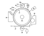
図2に帯電部材を有する電子写真装置の概略構成例を示す。帯電部材に接触配置され、帯電部材によって帯電可能な被帯電体としての電子写真感光体(以降、「感光体」と略)21は、導電性支持体21bと、支持体21b上に形成した感光層21aとからなり、ドラム形状を有する。そして、軸21cを中心に図上時計方向に所定の周速度をもって回転駆動される。帯電ローラ10は感光体21に接触配置されて感光体を所定の極性・電位に帯電(一次帯電)する。帯電ローラ10は、芯金11と、芯金11上に形成した弾性層12とからなり、芯金11の両端部を不図示の押圧手段で電子写真感光体21に押圧されており、感光体21の回転駆動に伴い従動回転する。電源23で摺擦電源23aにより、芯金11の所定の直流(DC)バイアスが印加されることで感光体21が所定の極性・電位に接触帯電される。帯電ローラ10で周面が帯電された感光体21は、次いで露光手段24により目的画像情報の露光(レーザービーム走査露光、原稿画像のスリット露光など)を受けることで、その周面に目的の画像情報に対した静電潜像が形成される。その静電潜像は、次いで、現像部材25により、トナー画像として順次に可視像化されていく。このトナー画像は、次いで、転写手段26により不図示の給紙手段部から感光体21の回転と同期取りされて適正なタイミングをもって感光体21と転写手段26との間の転写部へ搬送された転写材27に順次転写されていく。図2の転写手段26は転写ローラであり、転写材27の裏からトナーと逆極性の帯電を行うことで電子写真感光体21側のトナー画像が転写材27に転写されていく。表面にトナー画像の転写を受けた転写材27は、感光体21から分離されて不図示の定着手段へ搬送されて像定着を受け、画像形成物として出力される。あるいは、裏面にも像形成するものでは、不図示の、転写部への再搬送手段へ搬送される。像転写後の電子写真感光体21の周面は、弾性ブレードに代表されるクリーニング部材28によって感光体21の表面に残留しているトナーなどが除去されて洗浄面化される。清浄面化された感光体21は次のサイクルの電子写真画像形成プロセスが行われることになる。
FIG. 2 shows a schematic configuration example of an electrophotographic apparatus having a charging member. An electrophotographic photosensitive member (hereinafter abbreviated as “photosensitive member”) 21 that is disposed in contact with the charging member and can be charged by the charging member includes a
上記の一連の電子写真画像の形成プロセスにおいて、帯電ローラは感光体21とのニップ付近のギャップにおいて放電を生じさせることによって、感光体の表面を帯電している。その際に、帯電ローラの近傍に発生する放電生成物や感光体表面の磨耗粉等が感光体の表面に付着する。そして、それらが帯電ローラと感光体とのニップ部において感光体の表面に押し付けられることによって感光体の表面に蓄積されていく。そして、感光体と弾性ブレードとの摩擦係数が徐々に上昇していく。やがて、感光体と弾性ブレードとの間の高い摩擦係数によって弾性ブレードが振動し始め、感光体の表面の残留トナーが十分に除去できなくなっていく。その結果、次のサイクルの電子写真画像形成プロセスは、表面に残留トナーが付着した感光体に行われることとなる。
In the series of electrophotographic image forming processes described above, the charging roller charges the surface of the photoconductor by causing discharge in a gap near the nip with the
ここで、感光体と弾性ブレードとの間の摩擦係数の上昇は、弾性体からなる表面層を有する帯電ローラにおいて顕著に現れた。その理由は、弾性体からなる表面層を有する帯電ローラは、その表面が柔軟であるため、帯電ローラと感光体とのニップ部における接触面積が大きくなり、放電生成物等の摩擦係数の上昇の引き起こす物質を、感光体表面に、より固着させ易いことによるものと考えられる。 Here, the increase in the coefficient of friction between the photosensitive member and the elastic blade was conspicuous in the charging roller having the surface layer made of the elastic member. The reason is that a charging roller having a surface layer made of an elastic body has a flexible surface, so that the contact area at the nip portion between the charging roller and the photosensitive member increases, and the friction coefficient of discharge products and the like increases. It is considered that the substance to be caused is more easily fixed on the surface of the photoreceptor.
そこで、本発明者らは、感光体との間で適度なニップを得るための柔軟性を有するにもかかわらず、感光体の表面に放電生成物を固着させにくい帯電部材を得ることを目的として種々の検討を行った。 Therefore, the present inventors have aimed to obtain a charging member that has a flexibility to obtain an appropriate nip with the photoconductor, but hardly adheres the discharge product to the surface of the photoconductor. Various studies were conducted.
その結果、電子線の照射によって表面が硬化された領域が形成されてなり、かつ、この領域によって、球状シリカ粒子、球状アルミナ粒子および球状ジルコニア粒子から選択される少なくとも一つの球状粒子を、少なくともその一部が表面に露出した状態で支持されてなり、当該球状粒子によって表面を粗面化されている構成を有する弾性層を表面層として有する帯電部材によって上記の目的が達成できることを見出した。
以下、本発明の好適な実施の形態について説明する。
As a result, a region whose surface is hardened by irradiation with an electron beam is formed, and at least one spherical particle selected from spherical silica particles, spherical alumina particles and spherical zirconia particles is formed by this region. It has been found that the above object can be achieved by a charging member that is supported in a state where a part thereof is exposed on the surface and has an elastic layer having a surface roughened by the spherical particles as a surface layer.
Hereinafter, preferred embodiments of the present invention will be described.
<帯電部材>
本発明に係る帯電部材は、導電性の支持体と、表面層である弾性層とを有する。また、前記弾性層の表面は、球状シリカ粒子、球状アルミナ粒子および球状ジルコニア粒子から選ばれる少なくとも一つの球状粒子により粗面化されている。また、前記弾性層は、電子線の照射によって硬化された領域を表面に有しており、球状粒子のうちの少なくとも一部の粒子について、各粒子の一部分が前記弾性層の表面に露出した状態で硬化された領域によって支持されている。
<Charging member>
The charging member according to the present invention includes a conductive support and an elastic layer that is a surface layer. The surface of the elastic layer is roughened with at least one spherical particle selected from spherical silica particles, spherical alumina particles, and spherical zirconia particles. The elastic layer has a region hardened by electron beam irradiation on the surface, and at least some of the spherical particles are in a state where a part of each particle is exposed on the surface of the elastic layer. Supported by the cured area.
図1に、本発明の帯電部材としての帯電ローラの概略構成例を示す。 FIG. 1 shows a schematic configuration example of a charging roller as a charging member of the present invention.
帯電ローラ10は、芯金11と、芯金11上に形成した弾性層12とからなっている。本発明に係る帯電部材は、図2に示す電子写真装置の帯電ローラ10として用いることができる。
The charging
図3は本発明の帯電ローラ表面の形態を表す模式図である。本発明に係る帯電ローラの弾性層は、シリカ、アルミナ、ジルコニアから選ばれる少なくとも1つの球状粒子31を含有し、この球状粒子により表面が粗面化されている。また、弾性層の表面は電子線照射による硬化処理がなされており、前述した球状粒子のうちの少なくとも一部の粒子について、各粒子の一部分は弾性層表面に露出すると共に、弾性層の、電子線照射により硬化された領域13により支持されている。
FIG. 3 is a schematic view showing the form of the surface of the charging roller of the present invention. The elastic layer of the charging roller according to the present invention contains at least one
球状粒子が硬化領域13によって支持されている為、弾性層が感光体等の被帯電体に当接した場合でも、そのニップにおいて、球状粒子が弾性層内に埋没し難くなっている。その結果、ニップにおいても、高硬度な球状粒子は、弾性層の表面にその一部分を露出した状態で表面の凹凸形状を維持することができ、感光体との接触面積を小さくすることができる。また、球状シリカ粒子、球状アルミナ粒子および球状ジルコニア粒子は、球状の形状ゆえに、弾性層表面から露出した部分が感光体に直接接触しても、感光体の傷つきや、感光体の表面の過度な磨耗を抑制できる。
Since the spherical particles are supported by the cured
また、電子線照射による硬化処理は、弾性層の表面部分のみを硬化することが可能で、弾性体の内部、すなわち、深層部分は低い硬度(MD−1硬度で50以上80未満)を維持することができる。そのため、帯電ローラ全体を高硬度化した場合、例えば、弾性層全体のMD−1硬度を80度以上にまで高硬度化した場合に認められる、帯電ローラと被帯電体とのニップの幅の減少に伴う当接不良による帯電不良や、帯電ローラ表面に経時的にトナーや外添剤の付着することによる画像不良の発生を抑制できる。 Moreover, the hardening process by electron beam irradiation can harden only the surface part of an elastic layer, and the inside of an elastic body, ie, a deep layer part, maintains low hardness (MD-1 hardness is 50 or more and less than 80). be able to. Therefore, when the hardness of the entire charging roller is increased, for example, when the MD-1 hardness of the entire elastic layer is increased to 80 degrees or more, the reduction in the nip width between the charging roller and the object to be charged is reduced. Therefore, it is possible to suppress the occurrence of charging failure due to contact failure due to contact, and image failure due to toner or external additives adhering to the charging roller surface over time.
(導電性の支持体)
導電性支持体は、導電性を有し、弾性層等を支持可能であって、かつ、帯電ローラとしての強度を維持し得るものであればよい。
(Conductive support)
The conductive support is not particularly limited as long as it has conductivity, can support the elastic layer and the like, and can maintain the strength as the charging roller.
(弾性層)
弾性層は、ベースポリマーまたはその架橋物と、球状粒子とを含む。ベースポリマーとしては、帯電部材の実使用温度範囲で弾性層にゴム弾性を持たせることのできる材料が用いられる。ベースポリマーとしては、熱可塑性エラストマーおよび熱硬化性ゴムが挙げられる。
(Elastic layer)
The elastic layer includes a base polymer or a cross-linked product thereof and spherical particles. As the base polymer, a material capable of imparting rubber elasticity to the elastic layer within the actual use temperature range of the charging member is used. Examples of the base polymer include thermoplastic elastomers and thermosetting rubbers.
熱硬化性ゴムは、原料ゴムに架橋剤を配合したゴム組成物である。ここで、原料ゴムの具体例を以下に挙げる。天然ゴム(NR)、イソプレンゴム(IR)、ブタジエンゴム(BR)、スチレン−ブタジエンゴム(SBR)、ブチルゴム(IIR)、エチレン−プロピレン−ジエン3元共重合体ゴム(EPDM)、エピクロルヒドリンホモポリマー(CHC)、エピクロルヒドリン−エチレンオキサイド共重合体(CHR)、エピクロルヒドリン−エチレンオキサイド−アリルグリシジルエーテル3元共重合体(CHR−AGE)、アクリロニトリル−ブタジエン共重合体(NBR)、アクリロニトリル−ブタジエン共重合体の水添物(H−NBR)、クロロプレンゴム(CR)、アクリルゴム(ACM、ANM)等。
また、熱可塑性エラストマーの具体例を以下に挙げる。熱可塑性ポリオレフィン系熱可塑性エラストマー、ポリスチレン系熱可塑性エラストマー、ポリエステル系熱可塑性エラストマー、ポリウレタン系熱可塑性エラストマー、ポリアミド系熱可塑性エラストマー、塩ビ系熱可塑性エラストマー等の熱可塑性エラストマー等。
The thermosetting rubber is a rubber composition obtained by blending a raw material rubber with a crosslinking agent. Here, specific examples of the raw rubber will be given below. Natural rubber (NR), isoprene rubber (IR), butadiene rubber (BR), styrene-butadiene rubber (SBR), butyl rubber (IIR), ethylene-propylene-diene terpolymer rubber (EPDM), epichlorohydrin homopolymer ( CHC), epichlorohydrin-ethylene oxide copolymer (CHR), epichlorohydrin-ethylene oxide-allyl glycidyl ether terpolymer (CHR-AGE), acrylonitrile-butadiene copolymer (NBR), acrylonitrile-butadiene copolymer Hydrogenated products (H-NBR), chloroprene rubber (CR), acrylic rubber (ACM, ANM), etc.
Specific examples of the thermoplastic elastomer are given below. Thermoplastic polyolefin-based thermoplastic elastomers, polystyrene-based thermoplastic elastomers, polyester-based thermoplastic elastomers, polyurethane-based thermoplastic elastomers, polyamide-based thermoplastic elastomers, PVC-based thermoplastic elastomers, and the like.
本発明に用いる弾性層には球状シリカ粒子、球状アルミナ粒子および球状ジルコニア粒子から選ばれる少なくとも一つの球状粒子が配合される。シリカ、アルミナ、ジルコニアからなる球形粒子は高硬度(新モース硬度で7以上)である為、後述する砥石などを用いた研摩工程においても粒子そのものが研削されることが無く、球状を維持して弾性層表面に存在することができる。球状粒子は、主成分がシリカ、アルミナ、ジルコニアからなる粒子であって、Na2O、K2O、Fe2O3、MnO、CaO、MgO、TiO2等の不純物を含んでいても良い。球状粒子中のこれらの不純物の含有量は5質量%以下であることが好ましい。 The elastic layer used in the present invention contains at least one spherical particle selected from spherical silica particles, spherical alumina particles and spherical zirconia particles. Since spherical particles made of silica, alumina, and zirconia have high hardness (new Mohs hardness of 7 or more), the particles themselves are not ground even in a polishing process using a grindstone, which will be described later, and maintain a spherical shape. It can be present on the elastic layer surface. The spherical particles are particles mainly composed of silica, alumina, and zirconia, and may contain impurities such as Na 2 O, K 2 O, Fe 2 O 3 , MnO, CaO, MgO, and TiO 2 . The content of these impurities in the spherical particles is preferably 5% by mass or less.
球状粒子の粒子径は2μm以上80μm以下であることが好ましい。粒子径が2μm以上であれば、粒子径が小さいことによる感光体との接触面積の増加を抑制することができる。また、粒子径が80μm以下であれば、粒子の大きさによる弾性層の表面粗さの増大による、帯電ローラ表面のトナー等の汚れを抑制できる。さらに好ましい球状粒子の粒子径の範囲としては5μm以上40μm以下である。これらの球状粒子によって、弾性層の表面は粗面化されており、粗面化の程度としては帯電部材表面(弾性層の表面)の十点平均粗さRzが3μm以上20μm以下であることが好ましい。 The particle diameter of the spherical particles is preferably 2 μm or more and 80 μm or less. If the particle diameter is 2 μm or more, an increase in the contact area with the photoreceptor due to the small particle diameter can be suppressed. Further, when the particle diameter is 80 μm or less, it is possible to suppress the contamination of the toner on the surface of the charging roller due to the increase in the surface roughness of the elastic layer due to the particle size. A more preferable range of the particle diameter of the spherical particles is 5 μm or more and 40 μm or less. The surface of the elastic layer is roughened by these spherical particles, and the degree of roughening is such that the 10-point average roughness Rz of the charging member surface (the surface of the elastic layer) is 3 μm or more and 20 μm or less. preferable.
さらに、球状粒子の球形度に関しては下記に示す形状係数SF1の値が100以上160以下であることが好ましい。ここで、形状係数SF1は下記式(1)で表される指数であり、100に近いほど球形に近いことを意味している。形状係数が160以下であれば、球状粒子が弾性層表面に露出して感光体に直接接触していても、感光体を傷つけたり、感光体の磨耗を抑制することができる。 Furthermore, regarding the sphericity of the spherical particles, the value of the shape factor SF1 shown below is preferably 100 or more and 160 or less. Here, the shape factor SF1 is an index represented by the following formula (1), and the closer to 100, the closer to a spherical shape. If the shape factor is 160 or less, even if the spherical particles are exposed on the surface of the elastic layer and are in direct contact with the photoconductor, the photoconductor can be damaged or the photoconductor can be prevented from being worn.
球状粒子の粒子径は以下の方法によって求められる「長さ平均粒子径」である。まず、球状粒子を走査型電子顕微鏡(日本電子株式会社製、商品名:JEOL LV5910)で観察、画像撮影を実施し、撮影画像を画像解析ソフト(商品名:Image−Pro Plus、プラネトロン社製)を用いて解析する。解析は写真撮影時のミクロンバーから単位長さあたりの画素数をキャリブレーションし、写真から無作為に選択した50個の粒子について、画像上の画素数から定方向径を測定し、算術平均粒子直径を求め、球状粒子の粒子径とする。 The particle diameter of the spherical particles is a “length average particle diameter” determined by the following method. First, the spherical particles were observed with a scanning electron microscope (manufactured by JEOL Ltd., trade name: JEOL LV5910) and imaged, and the captured image was image analysis software (trade name: Image-Pro Plus, produced by Planetron). Analyze using In the analysis, the number of pixels per unit length is calibrated from the micron bar at the time of photography, and for 50 particles randomly selected from the photograph, the directional diameter is measured from the number of pixels on the image, and the arithmetic average particle The diameter is obtained and used as the particle diameter of the spherical particles.
本発明に用いる球状粒子の形状係数SF1の測定は以下の方法によって求められる。粒子径と同様に走査型電子顕微鏡で撮影した画像情報を画像解析装置(ニコレ社製、商品名:Lusex3)に入力し、無作為に選んだ50個の粒子像について、下記式(1)によって算出する。
SF1={(MXLNG)2/AREA}×(π/4)×(100)・・・・(1)
(ただし、MXLNGは粒子の絶対最大長を、AREAは粒子の投影面積を表す)。
The shape factor SF1 of the spherical particles used in the present invention is measured by the following method. Similar to the particle size, image information taken with a scanning electron microscope is input to an image analyzer (trade name: Lusex3, manufactured by Nicole), and 50 particle images randomly selected are expressed by the following equation (1). calculate.
SF1 = {(MXLNG) 2 / AREA} × (π / 4) × (100) (1)
(Where MXLNG is the absolute maximum length of the particle and AREA is the projected area of the particle).
また、球形粒子の比表面積はJIS Z8830(2001年)に準拠して測定した値で、10m2/g以下が好ましい。球状粒子の比表面積が10m2/g以下とすることで、球状粒子による弾性層の補強効果を小さくできる。これによって、弾性層の高硬度化を抑えることができる。弾性層に配合される球形粒子は単一種類を配合しても構わないし、2種類以上をブレンドして配合しても構わない。 The specific surface area of the spherical particles is a value measured according to JIS Z8830 (2001), and is preferably 10 m 2 / g or less. When the specific surface area of the spherical particles is 10 m 2 / g or less, the reinforcing effect of the elastic layer by the spherical particles can be reduced. Thereby, the increase in hardness of the elastic layer can be suppressed. The spherical particles to be blended in the elastic layer may be blended in a single type or in a blend of two or more types.
この場合、弾性層中の球状粒子の含有量は合計で、弾性層の全質量に対して、10質量部以上100質量部以下が好ましい。10質量部以上であれば粒子が充分な量、表面に存在することができ、感光体との接触面積を特に小さくする事ができる。また、100質量部以下であれば粒子の配合量が多くなって弾性層が硬くなるのを抑制できる。 In this case, the total content of the spherical particles in the elastic layer is preferably 10 parts by mass or more and 100 parts by mass or less with respect to the total mass of the elastic layer. If the amount is 10 parts by mass or more, a sufficient amount of particles can be present on the surface, and the contact area with the photoreceptor can be particularly reduced. Moreover, if it is 100 mass parts or less, it can suppress that the compounding quantity of particle | grains increases and an elastic layer becomes hard.
また、弾性層中には、導電剤、充填剤、加工助剤、老化防止剤、架橋助剤、架橋促進剤、架橋促進助剤、架橋遅延剤、分散剤等を含有させることができる。導電剤の具体例を以下に挙げる。
・カーボンブラック、グラファイト等の炭素材料;
・酸化チタン、酸化錫等の酸化物;Cu、Ag等の金属;
・酸化物や金属を粒子表面に被覆して導電化した導電粒子等の電子導電剤;
・過塩素酸リチウム、過塩素酸ナトリウム、過塩素酸カルシウム等の無機イオン物質;
・ラウリルトリメチルアンモニウムクロライド、ステアリルトリメチルアンモニウムクロライド等の陽イオン性界面活性剤;
・ラウリルベタイン等の両性イオン界面活性剤;
・過塩素酸テトラエチルアンモニウム等の第四級アンモニウム塩;
・有機酸リチウム(トリフルオロメタンスルホン酸リチウム)等の塩等のイオン導電剤。
The elastic layer can contain a conductive agent, a filler, a processing aid, an anti-aging agent, a crosslinking aid, a crosslinking accelerator, a crosslinking acceleration aid, a crosslinking retarder, a dispersant, and the like. Specific examples of the conductive agent are listed below.
-Carbon materials such as carbon black and graphite;
-Oxides such as titanium oxide and tin oxide; metals such as Cu and Ag;
-Electronic conductive agents such as conductive particles that are made conductive by coating the surface of the oxide or metal;
・ Inorganic ionic substances such as lithium perchlorate, sodium perchlorate, calcium perchlorate;
-Cationic surfactants such as lauryltrimethylammonium chloride and stearyltrimethylammonium chloride;
-Zwitterionic surfactants such as lauryl betaine;
-Quaternary ammonium salts such as tetraethylammonium perchlorate;
An ionic conductive agent such as a salt of organic acid lithium (lithium trifluoromethanesulfonate) or the like.
特に断らない限り本明細書においては、弾性層とは、表面層としての弾性層(表面弾性層と称することもある)を意味する。本発明においては導電性支持体と表面弾性層との間には接着層を形成することも出来る。また、弾性層を多層化すること(表面弾性層の他に弾性層を一層以上有すること)も可能である。ただし、多層化する場合は最表面に球状粒子を含有する層(表面弾性層)を形成する必要がある。また、弾性層を多層化する場合は、後述するチューブ状に押出す方法、あるいはクロスヘッドを使用して押出す方法において、多層押出機を使用して各層を同時成形することが好ましい。 Unless otherwise specified, in this specification, the elastic layer means an elastic layer as a surface layer (sometimes referred to as a surface elastic layer). In the present invention, an adhesive layer can be formed between the conductive support and the surface elastic layer. It is also possible to make the elastic layer multi-layered (having one or more elastic layers in addition to the surface elastic layer). However, in the case of multilayering, it is necessary to form a layer containing spherical particles (surface elastic layer) on the outermost surface. When the elastic layer is multilayered, it is preferable to simultaneously mold each layer using a multilayer extruder in a method of extruding into a tube shape described later or a method of extruding using a cross head.
本発明においては生産工程を簡素化する効果を最大とする為に、弾性層は単層であること、すなわち、本発明に係る帯電部材における唯一の弾性層であることが最も好ましい。そして、この場合における弾性層の厚さとしては、被帯電体とのニップ幅を確保するために、0.8mm以上4.0mm以下、特には、1.2mm以上3.0mm以下が好ましい。 In the present invention, in order to maximize the effect of simplifying the production process, the elastic layer is most preferably a single layer, that is, the only elastic layer in the charging member according to the present invention. In this case, the thickness of the elastic layer is preferably 0.8 mm or more and 4.0 mm or less, particularly 1.2 mm or more and 3.0 mm or less in order to secure a nip width with the charged body.
<帯電部材の製造方法>
本発明の帯電部材の製造方法は以下の(工程1)〜(工程3)を有する。
(工程1)導電性の支持体上に、球状シリカ粒子、球状アルミナ粒子および球状ジルコニア粒子から選ばれる少なくとも一つの球状粒子を含むゴム層を形成する工程。
(工程2)該ゴム層の表面を研摩して該球状粒子のうちの少なくとも一部の粒子について、各粒子の一部分を表面に露出させる工程。
(工程3)研摩後のゴム層の表面に電子線を照射して、表面をさらに硬化させる工程。
<Method for manufacturing charging member>
The manufacturing method of the charging member of the present invention includes the following (Step 1) to (Step 3).
(Step 1) A step of forming a rubber layer containing at least one spherical particle selected from spherical silica particles, spherical alumina particles and spherical zirconia particles on a conductive support.
(Step 2) A step of polishing the surface of the rubber layer to expose at least some of the spherical particles to expose a part of each particle on the surface.
(Step 3) A step of further curing the surface by irradiating the surface of the rubber layer after polishing with an electron beam.
以下に各工程を説明する。 Each step will be described below.
(工程1)
まず、導電性の支持体上に、球状粒子を含むゴム層を形成する。なお、ゴム層とは、球状粒子を含む混合物(ベースポリマーおよび添加剤等を含むことができる)を所定の形状に成形したものである。以下に具体例を説明する。弾性層を構成するベースポリマーとシリカ、アルミナ、ジルコニアから選ばれる少なくとも1つの球状粒子との混合物を調製する。なお、ベースポリマーが熱可塑性ゴムの場合、当該混合物をゴム組成物と称する。また、ベースポリマーが未加硫の熱硬化性ゴムの場合、当該混合物を未加硫ゴム組成物と称する。
続いて、導電性の支持体の周面をゴム組成物また未加硫ゴム組成物で被覆してローラ形状に成形する。ここで、支持体の周面をゴム組成物で被覆して得たローラを、単にゴムローラと称する。また、支持体の周面を未加硫ゴム組成物で被覆して得たローラを未加硫ゴムローラと称する。
次いで、未加硫ゴムローラについては、架橋操作等を行い固化し、加硫ゴムローラを得る。
(Process 1)
First, a rubber layer containing spherical particles is formed on a conductive support. The rubber layer is formed by molding a mixture containing spherical particles (which can include a base polymer and additives) into a predetermined shape. A specific example will be described below. A mixture of a base polymer constituting the elastic layer and at least one spherical particle selected from silica, alumina, and zirconia is prepared. In addition, when the base polymer is a thermoplastic rubber, the mixture is referred to as a rubber composition. When the base polymer is an unvulcanized thermosetting rubber, the mixture is referred to as an unvulcanized rubber composition.
Subsequently, the peripheral surface of the conductive support is coated with a rubber composition or an unvulcanized rubber composition and molded into a roller shape. Here, a roller obtained by coating the peripheral surface of the support with a rubber composition is simply referred to as a rubber roller. A roller obtained by coating the peripheral surface of the support with an unvulcanized rubber composition is referred to as an unvulcanized rubber roller.
Next, the unvulcanized rubber roller is solidified by performing a crosslinking operation or the like to obtain a vulcanized rubber roller.
ゴム組成物または未加硫ゴム組成物をローラ形状に成形する方法としては、下記(a)〜(c)の方法を挙げることができる。
(a)ゴム組成物を押出機によりチューブ状に押出成形し、これに芯金を挿入する方法;
(b)ゴム組成物を、クロスヘッドを装着した押出機により、芯金を中心に円筒形に共押出し、所望の外径の成形体を得る方法;
(c)ゴム組成物を射出成形機を使用して、所望の外径の金型内部に注入して成形体を得る方法。
Examples of the method for forming the rubber composition or the unvulcanized rubber composition into a roller shape include the following methods (a) to (c).
(A) A method of extruding a rubber composition into a tube shape by an extruder and inserting a metal core into the tube;
(B) A method in which a rubber composition is coextruded into a cylindrical shape around a core metal by an extruder equipped with a crosshead to obtain a molded body having a desired outer diameter;
(C) A method of obtaining a molded product by injecting a rubber composition into a mold having a desired outer diameter using an injection molding machine.
中でも、上記(b)は、連続生産が容易で、工程数が少なく、低コストでの製造に適している為、最も好ましい。 Among them, the above (b) is most preferable because continuous production is easy, the number of steps is small, and it is suitable for production at low cost.
未加硫ゴムローラの加硫は加熱処理によって行う。加熱処理の方法の具体例としては、ギアオーブンによる熱風炉加熱、遠赤外線による過熱加硫、加硫缶による水蒸気加熱などを挙げることができる。中でも熱風炉加熱や遠赤外線過熱は、連続生産に適しているため好ましい。 Vulcanization of the unvulcanized rubber roller is performed by heat treatment. Specific examples of the heat treatment method include hot blast furnace heating using a gear oven, superheat vulcanization using far infrared rays, and steam heating using a vulcanizer. Of these, hot stove heating and far-infrared overheating are preferable because they are suitable for continuous production.
(工程2)
工程(1)によって得られたゴムローラまたは加硫ゴムローラのゴム層表面を研磨処理することによって、ゴム層の表面に球状粒子のうちの少なくとも一部の粒子について、各粒子の一部分を露出させる。球状粒子としては、シリカ、アルミナおよびジルコニアのうちの少なくとも1つを用いる。これらの粒子は一般的に硬いため、砥石などを用いた研摩工程において粒子そのものが研削されにくく、研摩処理後も球状を維持し易く、また、ゴム層表面に存在することができる。ゴムローラ(ゴム層)の表面を研削する方法の例としては、砥石またはローラをローラのスラスト方向に移動して研削するトラバースの研削方式と、ローラを芯金軸の中心に回転させながらローラ長さより幅広の研削砥石を往復させずに切り込むプランジカットの研削方式が挙げられる。プランジカットの円筒研削方式はゴムローラの全幅を一度に研削できる利点があり、トラバースの円筒研削方式より加工時間が短くすることができるため、より好ましい。
(Process 2)
By polishing the surface of the rubber layer of the rubber roller or vulcanized rubber roller obtained in the step (1), a part of each particle of the spherical particles is exposed on the surface of the rubber layer. As the spherical particles, at least one of silica, alumina, and zirconia is used. Since these particles are generally hard, the particles themselves are difficult to be ground in a polishing process using a grindstone and the like, and are easily maintained in a spherical shape after the polishing treatment, and can be present on the surface of the rubber layer. Examples of methods for grinding the surface of a rubber roller (rubber layer) include: a traverse grinding method in which a grinding wheel or roller is moved in the thrust direction of the roller for grinding, and the roller length while rotating the roller around the center of the core metal shaft. A plunge-cut grinding method in which a wide grinding wheel is cut without reciprocating. The plunge cut cylindrical grinding method has the advantage that the entire width of the rubber roller can be ground at once, and is more preferable because the processing time can be shortened compared to the traverse cylindrical grinding method.
(工程3)
最後に、研摩した後のゴム層の表面(ゴムローラ表面)に電子線を照射して、表面の硬化処理を行い、表面に硬化された領域を有する弾性層を形成する。
(Process 3)
Finally, the surface of the rubber layer after polishing (the surface of the rubber roller) is irradiated with an electron beam to perform a surface curing process, thereby forming an elastic layer having a cured region on the surface.
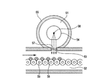
図5に電子線照射装置の概略図を示す。本発明に用いることのできる電子線照射装置としては、研摩後のゴムローラを回転させながらローラ表面に電子線を照射するものを好適に用いることができる。例えば、図5に示すように、電子線発生部51と照射室52と照射口53とを備えるものである。
FIG. 5 shows a schematic diagram of an electron beam irradiation apparatus. As an electron beam irradiation apparatus that can be used in the present invention, an apparatus that irradiates the surface of a roller with an electron beam while rotating a polished rubber roller can be suitably used. For example, as shown in FIG. 5, an
電子線発生部51は、電子線を発生するターミナル54と、ターミナル54で発生した電子線を真空空間(加速空間)で加速する加速管55とを有するものである。また電子線発生部の内部は、電子が気体分子と衝突してエネルギーを失うことを防ぐため、不図示の真空ポンプ等により10−3Pa以上10−6Pa以下の真空に保たれている。不図示の電源によりフィラメント56に電流を通じて加熱するとフィラメント56は熱電子を放出し、この熱電子のうち、ターミナル54を通過したものだけが電子線として有効に取り出される。そして、電子線の加速電圧により加速管55内の加速空間で加速された後、照射口箔57を突き抜け、照射口53の下方の照射室52内を搬送される研摩後のゴムローラ58に照射される。研摩後のゴムローラ58に電子線を照射する場合には、照射室52の内部は窒素雰囲気とすることができる。また、研摩後のゴムローラ58はローラ回転用部材59で回転させて照射室内を搬送手段により、図5において左側から右側に移動する。尚、電子線発生部51及び照射室52の周囲は電子線照射時に二次的に発生するX線が外部へ漏出しないように、不図示の鉛遮蔽が施されている。
The
照射口箔57は金属箔からなり、電子線発生部内の真空雰囲気と照射室内の空気雰囲気とを仕切るものであり、また照射口箔57を介して照射室内に電子線を取り出すものである。上述したように、ローラの照射に電子線を応用する場合には、ローラが電子線を照射される照射室52の内部は窒素雰囲気とすることができる。よって、電子線発生部51と照射室52との境界に設ける照射口箔57は、ピンホールがなく、電子線発生部内の真空雰囲気を十分維持できる機械的強度があり、電子線が透過しやすいことが望ましい。その為、照射口箔57は比重が小さく、肉厚の薄い金属が望ましく、通常、アルミニウムやチタン箔が使用される。電子線による効果処理条件は電子線の加速電圧と線量によって決定される。加速電圧は硬化処理深さ(硬化処理厚さ、または硬化領域の厚みとも呼ぶ)に影響し、本発明に用いる加速電圧の条件としては、低エネルギー領域である40kV以上300kV以下が好ましい。40kV以上であれば、本発明の効果を得る為の充分な硬化処理深さを容易に得ることができる。また、300kV以下とすることで、電子線照射装置が大型化して装置コストが増大する事を特に抑えることができる。さらに好ましい加速電圧の条件としては80kV以上150kV以下である。
The
電子線照射における電子線の線量は、下記式(2)で定義される。
D = (K・I)/V ・・・・・・ (2)
ここで、Dは線量(kGy)、Kは装置定数、Iは電子電流(mA)、Vは処理スピード(m/min)である。装置定数Kは、装置個々の効率を表す定数であって、装置の性能の指標である。装置定数Kは一定の加速電圧の条件で、電子電流と処理スピードを変えて線量を測定することによって求めることができる。電子線の線量測定は、線量測定用フィルムをローラ表面に貼り付け、これを実際に電子線照射装置で処理し、ローラ表面の測定用フィルムをフィルム線量計により測定することができる。
The dose of electron beam in electron beam irradiation is defined by the following formula (2).
D = (KI) / V (2)
Here, D is a dose (kGy), K is an apparatus constant, I is an electron current (mA), and V is a processing speed (m / min). The device constant K is a constant representing the efficiency of each device, and is an index of device performance. The apparatus constant K can be obtained by measuring the dose while changing the electron current and the processing speed under the condition of a constant acceleration voltage. The dose measurement of the electron beam can be performed by attaching a dose measurement film on the roller surface, actually processing it with an electron beam irradiation apparatus, and measuring the measurement film on the roller surface with a film dosimeter.
その際、線量測定用フィルムは商品名:FWT−60、フィルム線量計は商品名:FWT−92D型(いずれもFarWest Technology社製)を使用することができる。本発明に用いる電子線の線量は30kGy以上3000kGy以下が好ましい。30kGy以上であれば本発明の効果を得る為に充分な表面硬度を容易に得ることができる。また、3000kV以下とすることで、電子線照射装置が大型化すること、または処理時間が増大することによる製造コストの増大を特に抑えることができる。さらに好ましい電子線量の条件としては200kGy以上2000kGy以下である。本発明において弾性層表面に露出している球状粒子は電子線により硬化された領域によって支持されている。 At that time, a trade name: FWT-60 can be used as the dosimetry film, and a trade name: FWT-92D (both manufactured by FarWest Technology) can be used as the film dosimeter. The dose of the electron beam used in the present invention is preferably 30 kGy or more and 3000 kGy or less. If it is 30 kGy or more, sufficient surface hardness can be easily obtained to obtain the effects of the present invention. Moreover, by setting it as 3000 kV or less, it can suppress especially the increase in manufacturing cost by an electron beam irradiation apparatus enlarging or processing time increasing. More preferable electron dose conditions are 200 kGy or more and 2000 kGy or less. In the present invention, the spherical particles exposed on the surface of the elastic layer are supported by regions hardened by an electron beam.
図3に、本発明の帯電ローラ表面の形態を模式的に示した。図3(a)は硬化領域の厚みが厚い場合を、図3(b)は硬化領域の厚みが薄い場合を示している。硬化領域の厚みについては特に規定されるものではないが、使用する球状粒子の平均粒子径(長さ平均粒子径)の0.5倍以上であることが好ましい。 FIG. 3 schematically shows the form of the surface of the charging roller of the present invention. FIG. 3A shows a case where the thickness of the hardened region is thick, and FIG. 3B shows a case where the thickness of the hardened region is thin. The thickness of the cured region is not particularly defined, but is preferably 0.5 times or more the average particle size (length average particle size) of the spherical particles to be used.
硬化領域の厚みを、粒子径の0.5倍以上とすることによって、表面に露出している球状粒子が当接部で弾性層内に埋没することを、より確実に抑えることができる。最も好ましい硬化領域の厚みは球状粒子の平均粒子径以上(平均粒子径と同値以上)200μm以下である。電子線による硬化領域の厚みを200μm以下とすることで帯電ローラと感光体とのニップの幅を十分に確保することができる。 By setting the thickness of the cured region to 0.5 times or more the particle diameter, it is possible to more reliably suppress the spherical particles exposed on the surface from being buried in the elastic layer at the contact portion. The most preferable thickness of the cured region is not less than the average particle diameter of spherical particles (not less than the same value as the average particle diameter) and not more than 200 μm. By setting the thickness of the cured region by the electron beam to 200 μm or less, a sufficient nip width between the charging roller and the photoconductor can be secured.
前述したように、電子線による硬化処理深さは加速電圧によって変化する。また一般的に、被照射物質の密度によっても電子線の透過深さが異なることが知られている。そのため、実際の硬化処理された領域の厚みを確認する方法としてはユニバーサル硬度計を使用した表面硬度の測定を挙げることができる。 As described above, the curing depth by the electron beam varies depending on the acceleration voltage. In general, it is known that the transmission depth of an electron beam varies depending on the density of an irradiated material. Therefore, as a method for confirming the thickness of the actual cured region, surface hardness measurement using a universal hardness meter can be mentioned.
ユニバーサル硬度とは、圧子を、荷重をかけながら測定対象物に押し込むことにより求められる物性値であり、(試験荷重)/(試験荷重下での圧子の表面積)(N/mm2)として求められる。このユニバーサル硬度の測定は、例えば、Fischer社製超微小硬度計H−100V(商品名)等の硬度測定装置を用いて行うことが可能である。この測定装置では、四角錘などの圧子を、所定の比較的小さい試験荷重をかけながら被測定物に押し込み、所定の押し込み深さに達した時点でその押し込み深さから圧子が接触している表面積を求め、上記式よりユニバーサル硬度を求めるものである。つまり、定荷重測定条件で圧子を被測定物に押し込んだ際に、押し込まれた深さに対するそのときの応力をユニバーサル硬度として定義するものである。 Universal hardness is a physical property value obtained by pushing an indenter into a measurement object while applying a load, and is obtained as (test load) / (surface area of the indenter under the test load) (N / mm 2 ). . The universal hardness can be measured using, for example, a hardness measuring device such as an ultra micro hardness meter H-100V (trade name) manufactured by Fischer. In this measuring device, an indenter such as a square weight is pushed into an object to be measured while applying a predetermined relatively small test load, and when the predetermined indentation depth is reached, the surface area with which the indenter contacts from the indentation depth And universal hardness from the above formula. That is, when the indenter is pushed into the object to be measured under the constant load measuring condition, the stress at that time with respect to the pushed-in depth is defined as universal hardness.
図4にはユニバーサル硬さの測定例を示す。グラフの横軸は押し込み深さ(μm)であり、縦軸は硬度(N/mm2)である。図4より、押し込み深さに対する硬度変化が小さく、直線領域である横軸150μm以上200μm以下の測定領域から外挿される直線と測定曲線とのずれが生じる点の横軸値を硬化領域の厚みとして定義することが出来る。なお、図4の測定例の硬化領域の厚みは50μmである。
FIG. 4 shows an example of universal hardness measurement. The horizontal axis of the graph is the indentation depth (μm), and the vertical axis is the hardness (N / mm 2 ). From FIG. 4, the change in hardness with respect to the indentation depth is small, and the horizontal axis value at the point where the straight line extrapolated from the measurement area of the
以下に実施例によって本発明を更に詳細に説明するが、これらは、本発明を何ら限定するものではない。なお、以下、特に明記しない限り、「部」は「質量部」を意味しており、試薬等は特に指定のないものは市販の高純度品を用いた。なお各例では、帯電ローラを作製した。 The present invention will be described in more detail with reference to the following examples, but these examples do not limit the present invention. Hereinafter, unless otherwise specified, “parts” means “parts by mass”, and commercially available high-purity products were used unless otherwise specified. In each example, a charging roller was produced.
〔実施例1〕
(弾性層用未加硫ゴム組成物の調製)
下記の表1に示す材料を、6リットル加圧ニーダー(製品名:TD6−15MDX、トーシン社製)を用いて、充填率70vol%、ブレード回転数30rpmで16分間混合してA練りゴム組成物を得た。
[Example 1]
(Preparation of unvulcanized rubber composition for elastic layer)
The materials shown in Table 1 below were mixed using a 6 liter pressure kneader (product name: TD6-15MDX, manufactured by Toshin Co., Ltd.) for 16 minutes at a filling rate of 70 vol% and a blade rotation speed of 30 rpm. Got.

次いで、下記の表2に示す材料を、ロール径12インチ(0.30m)のオープンロールにて、前ロール回転数8rpm、後ロール回転数10rpm、ロール間隙2mmで、左右の切り返しを合計20回実施した。その後、ロール間隙を0.5mmとして薄通し10回を行い、弾性層用の未加硫ゴム組成物を得た。 Next, the materials shown in Table 2 below were subjected to a total of 20 turns on the left and right sides with an open roll having a roll diameter of 12 inches (0.30 m) at a front roll rotation speed of 8 rpm, a rear roll rotation speed of 10 rpm, and a roll gap of 2 mm. Carried out. Thereafter, the roll gap was set to 0.5 mm, and thinning was performed 10 times to obtain an unvulcanized rubber composition for an elastic layer.
(加硫ゴム層の成形)
直径6mm、長さ244mmの円柱形の導電性芯金(鋼製、表面はニッケルメッキ)の円柱面の軸方向中央部222mmに導電性加硫接着剤(商品名:メタロックU−20;東洋化学研究所製)を塗布し、80℃で30分間乾燥した。次に、上記未加硫ゴム組成物を、クロスヘッドを用いた押出成形装置を用いて、芯金を中心として同軸状に円筒形に成形しつつ、芯金と同時に押し出して、芯金の外周に未加硫ゴム組成物がコーティングされた直径8.8mmの未加硫ゴムローラを作製した。
(Molding of vulcanized rubber layer)
Conductive vulcanizing adhesive (trade name: METALOC U-20; Toyo Chemical Co., Ltd.) on the central portion 222 mm in the axial direction of the cylindrical surface of a cylindrical conductive core bar (steel, surface is nickel-plated) with a diameter of 6 mm and a length of 244 mm (Manufactured by Laboratory) and dried at 80 ° C. for 30 minutes. Next, the unvulcanized rubber composition is extruded simultaneously with the core metal while being formed into a cylindrical shape coaxially around the core metal using an extrusion molding apparatus using a cross head, and the outer periphery of the core metal An unvulcanized rubber roller having a diameter of 8.8 mm, which was coated with an unvulcanized rubber composition, was prepared.
その際、押出機は、シリンダー直径45mm(Φ45)、L/Dが20の押出機を使用し、押出時の温調はヘッド90℃、シリンダー90℃、スクリュー90℃とした。成形した未加硫ゴムローラの未加硫ゴム組成物の層の幅方向の両端部を切断し、未加硫ゴム組成物の層の軸方向の長さを226mmとした。 At that time, an extruder having a cylinder diameter of 45 mm (Φ45) and an L / D of 20 was used as the extruder, and the temperature during extrusion was 90 ° C., 90 ° C. cylinder, and 90 ° C. screw. Both ends in the width direction of the layer of the unvulcanized rubber composition of the molded unvulcanized rubber roller were cut, and the length in the axial direction of the layer of the unvulcanized rubber composition was 226 mm.
その後、電気炉にて温度160℃で40分間加熱して未加硫ゴム組成物の層を加硫して加硫ゴム層とした。続いて、加硫ゴム層の表面をプランジカットの研削方式の研磨機で研磨し、端部直径8.35mm、中央部直径8.50mmのクラウン形状の球状粒子の一部が露出した加硫ゴム層を有する加硫ゴムローラを得た。 Thereafter, the unvulcanized rubber composition layer was vulcanized by heating in an electric furnace at a temperature of 160 ° C. for 40 minutes to obtain a vulcanized rubber layer. Subsequently, the surface of the vulcanized rubber layer is polished with a plunge cut grinding type polishing machine, and a part of the crown-shaped spherical particles having an end diameter of 8.35 mm and a central diameter of 8.50 mm is exposed. A vulcanized rubber roller having a layer was obtained.
(加硫ゴム層の硬度測定)
電子線照射前の加硫ゴム層のMD−1硬度を測定した。測定にはマイクロ硬度計(商品名:MD−1 capa、高分子計器株式会社製)を用いて、温度23℃、相対湿度55%の環境において、ピークホールドモードで測定した。より詳しくは加硫ゴムローラを金属製の板の上に置き、金属製のブロックを置いて加硫ゴムローラが転がらないように簡単に固定し、金属板に対して垂直方向から加硫ゴムローラの中心に正確に、タイプAの測定端子を押し当ててから5秒後の値を読み取る。これを加硫ゴムローラの軸方向のゴム端部から30〜40mmの位置の両端部及び中央部の3箇所、かつそれぞれの周方向に3箇所ずつ、計9箇所を測定し、得られた測定値の平均値を加硫ゴム層のMD−1硬度とした。その結果、加硫ゴム層のMD−1硬度は76°であった。
(Measurement of hardness of vulcanized rubber layer)
The MD-1 hardness of the vulcanized rubber layer before electron beam irradiation was measured. For measurement, a micro hardness tester (trade name: MD-1 capa, manufactured by Kobunshi Keiki Co., Ltd.) was used, and the measurement was performed in a peak hold mode in an environment of a temperature of 23 ° C. and a relative humidity of 55%. More specifically, place the vulcanized rubber roller on a metal plate, place a metal block, and fix it easily so that the vulcanized rubber roller does not roll. From the direction perpendicular to the metal plate, center the vulcanized rubber roller. Exactly read the value 5 seconds after pressing the type A measuring terminal. The measured values obtained by measuring a total of 9 locations, 3 locations at both ends and a central portion at a position 30 to 40 mm from the rubber end in the axial direction of the vulcanized rubber roller, and 3 locations in each circumferential direction. Was the MD-1 hardness of the vulcanized rubber layer. As a result, the MD-1 hardness of the vulcanized rubber layer was 76 °.
(研摩後の加硫ゴム層の表面硬化処理)
得られた研摩後の加硫ゴムローラの表面(加硫ゴム層表面)に電子線を照射して硬化処理を行い、弾性層の表面に硬化された領域を有する帯電ローラを得た。電子線の照射には、最大加速電圧150kV・最大電子電流40mAの電子線照射装置(岩崎電気株式会社製)を用い、照射時には窒素ガスパージを行った。処理条件は加速電圧:150kV、電子電流:35mA、処理速度:1m/min、酸素濃度:100ppmであった。この際、電子線照射装置の加速電圧150kVにおける装置定数は37.8であり、式(2)より算出される線量は1323kGyであった。
(Surface curing treatment of vulcanized rubber layer after polishing)
The surface of the obtained vulcanized rubber roller after polishing (the surface of the vulcanized rubber layer) was irradiated with an electron beam and cured to obtain a charging roller having a cured region on the surface of the elastic layer. For the electron beam irradiation, an electron beam irradiation apparatus (manufactured by Iwasaki Electric Co., Ltd.) having a maximum acceleration voltage of 150 kV and a maximum electron current of 40 mA was used, and nitrogen gas purge was performed during irradiation. The treatment conditions were acceleration voltage: 150 kV, electron current: 35 mA, treatment speed: 1 m / min, and oxygen concentration: 100 ppm. At this time, the apparatus constant of the electron beam irradiation apparatus at an acceleration voltage of 150 kV was 37.8, and the dose calculated from the equation (2) was 1323 kGy.
(硬化領域の厚さの測定)
帯電ローラの表面硬度をユニバーサル硬度計にて測定することにより、硬化処理厚さを測定した。測定には超微小硬度計(商品名:H−100V、Fischer社製)を用いた。また、圧子には四角錘型ダイヤモンドを用いた。押し込み速度は下記式(3)の条件である。
dF/dt = 1000mN/240s ・・・・(3)
上記式(3)において、Fは力、tは時間を表す。
(Measurement of thickness of cured area)
The thickness of the curing process was measured by measuring the surface hardness of the charging roller with a universal hardness meter. An ultra-micro hardness meter (trade name: H-100V, manufactured by Fischer) was used for the measurement. A square pyramid diamond was used for the indenter. The pushing speed is a condition of the following formula (3).
dF / dt = 1000 mN / 240 s (3)
In the above formula (3), F represents force and t represents time.
図4に示すように、押し込み深さに対する硬度変化が小さい横軸150μm以上200μm以下の測定領域から外挿される直線と測定曲線とのずれが生じる点の横軸値を硬化領域の厚みとして求めた。その結果、硬化領域の厚さは90μmであった。 As shown in FIG. 4, the horizontal axis value at the point where the deviation between the measurement curve and the straight line extrapolated from the measurement area having a small hardness change with respect to the indentation depth is 150 μm or more and 200 μm or less was obtained as the thickness of the cured region. . As a result, the thickness of the cured region was 90 μm.
(表面粗さの測定)
帯電ローラ(弾性層)表面の十点平均粗さRzを測定した。測定は JIS B0601:1982に基づき、表面粗さ測定器(商品名:サーフコーダーSE3400、小坂研究所社製)を用いて行った。測定には、先端半径2μmのダイヤモンド製接触針を用いた。測定スピードは0.5mm/s、カットオフ周波数λcは0.8mm、基準長さは0.8mm、評価長さは8.0mmとした。測定は帯電ローラ1本当たり、軸方向3点×周方向2点の計6点について各々粗さ曲線を測定してRzの値を算出し、それらの6点のRzの平均値を求めて帯電ローラのRzの値とした。その結果、Rzは8.9μmであった。
(Measurement of surface roughness)
The ten-point average roughness Rz on the surface of the charging roller (elastic layer) was measured. The measurement was performed based on JIS B0601: 1982 using a surface roughness measuring device (trade name: Surfcoder SE3400, manufactured by Kosaka Laboratory). For the measurement, a diamond contact needle having a tip radius of 2 μm was used. The measurement speed was 0.5 mm / s, the cut-off frequency λc was 0.8 mm, the reference length was 0.8 mm, and the evaluation length was 8.0 mm. For each charging roller, the roughness curve was measured for a total of 6 points, 3 in the axial direction and 2 in the circumferential direction, to calculate the value of Rz, and the average value of Rz at those 6 points was obtained to charge The Rz value of the roller was used. As a result, Rz was 8.9 μm.
(画像評価)
評価に用いる電子写真装置として、レーザービームプリンター(商品名:LaserJet P1005 ヒューレット・パッカード製、A4紙縦出力用、クリーニング部材として弾性ブレードを使用)を用意した。当該レーザービームプリンター用のプロセスカートリッジに、上記で作製した帯電ローラを組み込み、上記のレーザ−ビームプリンターに装填した。温度23℃、相対湿度50%の環境下で、ベタ画像およびハーフトーン画像(電子写真感光体の回転方向と垂直方向に幅1ドットの線を間隔2ドットで描く画像)を各々1枚ずつ出力した。これらを各々、初期のベタ画像、および初期のハーフトーン画像と称する。
(Image evaluation)
As an electrophotographic apparatus used for evaluation, a laser beam printer (trade name: LaserJet P1005, manufactured by Hewlett Packard, for A4 paper longitudinal output, using an elastic blade as a cleaning member) was prepared. The charging roller prepared above was incorporated into the process cartridge for the laser beam printer, and loaded into the laser-beam printer. A solid image and a halftone image (an image in which a line with a width of 1 dot is drawn at intervals of 2 dots in the direction perpendicular to the rotation direction of the electrophotographic photosensitive member) are output one by one in an environment of a temperature of 23 ° C. and a relative humidity of 50%. did. These are respectively referred to as an initial solid image and an initial halftone image.
次に、1枚の電子写真画像を出力した後、電子写真感光体の回転を完全に停止させ、再び画像形成動作を再開するという間欠的な画像形成動作を繰り返して1000枚の電子写真画像を出力するという耐久試験を行った。このときに出力した画像は、2ドットの横線後に118ドットの余白が繰り返される、罫線状の画像である。 Next, after outputting one electrophotographic image, the rotation of the electrophotographic photosensitive member is completely stopped, and the intermittent image forming operation of restarting the image forming operation is repeated to obtain 1000 electrophotographic images. An endurance test of output was performed. The image output at this time is a ruled line image in which a 118-dot margin is repeated after a 2-dot horizontal line.
次いで、再び、ベタ画像およびハーフトーン画像を各々1枚ずつ出力した。これらを耐久試験後のベタ画像、および、耐久試験後のハーフトーン画像と称する。 Next, one solid image and one halftone image were output again. These are referred to as a solid image after the durability test and a halftone image after the durability test.
そして、得られた2枚のソリッド画像、および2枚のハーフトーン画像について、目視にて、帯電ムラに起因する濃度ムラの有無およびその程度を観察し、以下の基準にて評価した。 The obtained two solid images and the two halftone images were visually observed for the presence and level of density unevenness due to charging unevenness, and evaluated according to the following criteria.
(評価1)帯電性能(初期、耐久後)の評価
上記で得られた初期ベタ画像および初期ハーフトーン画像について、目視にて観察し、帯電ムラに起因する濃度ムラの有無を下記の基準で評価した。
(Evaluation 1) Evaluation of Charging Performance (Initial, After Endurance) The initial solid image and the initial halftone image obtained above are observed visually, and the presence or absence of density unevenness due to charging unevenness is evaluated according to the following criteria. did.
また、上記で得られた耐久試験後のベタ画像および耐久試験後のハーフトーン画像についても同様に観察、評価した。 The solid image after the durability test and the halftone image after the durability test obtained above were also observed and evaluated in the same manner.
これによって、本実施例に係る帯電ローラの初期および耐久試験後の帯電性能を知ることができる。
A:ベタ画像およびハーフトーン画像のいずれにも帯電ムラに起因する濃度ムラが認められない。
B:ハーフトーン画像にのみ帯電ムラに起因する軽微な濃度ムラが認められる。
C:ハーフトーン画像に帯電ムラが認められ、また、ベタ画像に帯電ムラに起因する軽微な濃度ムラが認められる。
D:ベタ画像およびハーフトーン画像の両方に帯電ムラに起因する明瞭な濃度ムラが認められる。
Thereby, it is possible to know the charging performance of the charging roller according to the present embodiment at the initial stage and after the durability test.
A: Density unevenness due to charging unevenness is not observed in both the solid image and the halftone image.
B: Minor density unevenness due to charging unevenness is observed only in the halftone image.
C: Charge unevenness is observed in the halftone image, and slight density unevenness due to the charge unevenness is recognized in the solid image.
D: Clear density unevenness due to charging unevenness is observed in both the solid image and the halftone image.
(評価2)クリーニング不良に起因する画像欠陥の有無の評価
上記耐久試験において出力した1000枚の画像について、目視にて、感光体のクリーニング不良に起因する画像欠陥の有無およびその程度を観察し、以下の基準にて評価した。
A:クリーニング不良に起因する画像欠陥が発生したプリントが1枚も認められない。
B:クリーニング不良に起因する極軽微な画像欠陥が発生しているプリント枚数が1枚以上、100枚未満。
C:クリーニング不良に起因する明瞭な画像欠陥が発生したプリント枚数が1枚以上、100枚未満。
D:クリーニング不良に起因する明瞭な画像欠陥が発生したプリント枚数が100枚以上。
(Evaluation 2) Evaluation of presence / absence of image defects due to poor cleaning For the 1000 images output in the durability test, the presence / absence and degree of image defects due to poor cleaning of the photoreceptor are visually observed, Evaluation was made according to the following criteria.
A: No prints in which image defects due to poor cleaning occurred are observed.
B: The number of prints in which an extremely slight image defect due to poor cleaning occurs is 1 or more and less than 100.
C: The number of prints in which clear image defects due to poor cleaning occurred is 1 or more and less than 100.
D: The number of prints in which clear image defects due to poor cleaning occurred is 100 or more.
(評価3)感光体と弾性ブレードとの摩擦係数の評価
上記の画像形成に用いたレーザープリンターの感光体の表面に、弾性ブレードをカウンター方向に当接させた状態で、当該感光体と弾性ブレードとの摩擦係数を測定した。
(Evaluation 3) Evaluation of Friction Coefficient between Photoreceptor and Elastic Blade With the elastic blade abutting in the counter direction on the surface of the photoreceptor of the laser printer used for the above image formation, the photoreceptor and elastic blade The friction coefficient was measured.
この測定によって、帯電ローラに起因する電子写真感光体の表面へのトナー等の固着の有無およびその程度を知ることができる。 By this measurement, it is possible to know whether or not the toner adheres to the surface of the electrophotographic photosensitive member due to the charging roller and the degree thereof.
測定方法としては、まず、上記のレーザープリンターから、感光体と弾性ブレードが組み込まれたユニット部分をプロセスカートリッジから取り出した。そして、感光体の駆動部に、トルクメーター(商品名;TP−10KCE 共和電業社製)を接続したモーターを接続し、当該モーターで、感光体を85rpmの回転数で回転させた時のトルクをトルクメーターで測定し、感光体の回転開始から4回転目の1周分の測定値の平均値を本実施例におけるトルクの値とした。
上記の評価1〜3の結果を表4に示す。
As a measurement method, first, the unit portion in which the photosensitive member and the elastic blade were incorporated was taken out from the process cartridge from the laser printer. Then, a motor connected to a torque meter (trade name: TP-10KCE manufactured by Kyowa Denki Co., Ltd.) is connected to the drive unit of the photoconductor, and the torque when the photoconductor is rotated at a rotational speed of 85 rpm with the motor is torqued. The average value of the measured values for one revolution of the fourth rotation from the start of rotation of the photosensitive member was taken as the torque value in this example.
Table 4 shows the results of the above evaluations 1 to 3.
〔実施例2〕
実施例1のA練りゴム組成物の組成を表4に示したように球状シリカ粒子−1を同質量部数の球状シリカ粒子−2(商品名:FB−40S、電気化学工業株式会社製)に変更した以外は、実施例1と同様にして加硫ゴムローラを作製した。実施例1と同様にして加硫ゴム層の硬度を測定した結果、75°であった。実施例1と同様に研摩後の加硫ゴムローラ表面の電子線照射による硬化処理を行い、帯電ローラを作製した。
[Example 2]
As shown in Table 4, the composition of the A-kneaded rubber composition of Example 1 was changed to spherical silica particles-2 (trade name: FB-40S, manufactured by Denki Kagaku Kogyo Co., Ltd.). Except for the change, a vulcanized rubber roller was produced in the same manner as in Example 1. As a result of measuring the hardness of the vulcanized rubber layer in the same manner as in Example 1, it was 75 °. In the same manner as in Example 1, the surface of the vulcanized rubber roller after polishing was cured by electron beam irradiation to produce a charging roller.
〔実施例3〕
実施例1のA練りゴム組成物に使用した球状シリカ粒子−1を同質量部数の球状シリカ粒子−3(商品名:HS−301、株式会社マイクロン社製)に変更した以外は、実施例1と同様に弾性層用未加硫ゴム組成物を調製し、研摩後の加硫ゴムローラを作製した。実施例1と同様に研摩後の加硫ゴムローラの加硫ゴム層の硬度を測定した結果、77°であった。実施例1と同様に研摩後の加硫ゴムローラ表面の電子線照射による硬化処理を行い、帯電ローラを作製した。
Example 3
Example 1 except that the spherical silica particles-1 used in the A-kneaded rubber composition of Example 1 were changed to spherical silica particles-3 (trade name: HS-301, manufactured by Micron Corporation) with the same parts by mass. In the same manner as above, an unvulcanized rubber composition for an elastic layer was prepared, and a vulcanized rubber roller after polishing was produced. As in Example 1, the hardness of the vulcanized rubber layer of the vulcanized rubber roller after polishing was measured and found to be 77 °. In the same manner as in Example 1, the surface of the vulcanized rubber roller after polishing was cured by electron beam irradiation to produce a charging roller.
〔実施例4〕
実施例1でのA練りゴム組成物に使用した球状シリカ粒子−1を同質量部数の球状シリカ粒子−4(商品名:HS−305、株式会社マイクロン社製)に変更した以外は、実施例1と同様に弾性層用未加硫ゴム組成物を調製し、研摩後の加硫ゴムローラを作製した。実施例1と同様に研摩後の加硫ゴムローラの加硫ゴム層の硬度を測定した結果、74°であった。実施例1と同様に研摩後の加硫ゴムローラ表面の電子線照射による硬化処理を行い、帯電ローラを作製した。
Example 4
Except that the spherical silica particles-1 used in the A-kneaded rubber composition in Example 1 were changed to spherical silica particles-4 having the same parts by mass (trade name: HS-305, manufactured by Micron Corporation), the examples The unvulcanized rubber composition for the elastic layer was prepared in the same manner as in No. 1, and a vulcanized rubber roller after polishing was produced. As in Example 1, the hardness of the vulcanized rubber layer of the vulcanized rubber roller after polishing was measured and found to be 74 °. In the same manner as in Example 1, the surface of the vulcanized rubber roller after polishing was cured by electron beam irradiation to produce a charging roller.
〔実施例5〕
実施例4の電子線の照射条件を、加速電圧:80kV、電子電流:35mA、処理速度:1m/min、酸素濃度:100ppmに変更した以外は、全て実施例4と同様にして帯電ローラを作製した。この際、電子線照射装置の加速電圧80kVにおける装置定数は20.4であり、式(2)より算出される線量は714kGyであった。実施例1と同様に帯電ローラの硬化処理厚さの測定と、表面粗さの測定、画像評価を行った。
Example 5
A charging roller was produced in the same manner as in Example 4 except that the electron beam irradiation conditions in Example 4 were changed to acceleration voltage: 80 kV, electron current: 35 mA, processing speed: 1 m / min, and oxygen concentration: 100 ppm. did. At this time, the apparatus constant at the acceleration voltage of 80 kV of the electron beam irradiation apparatus was 20.4, and the dose calculated from the equation (2) was 714 kGy. In the same manner as in Example 1, the thickness of the charging roller was measured, the surface roughness was measured, and the image was evaluated.
〔実施例6〕
実施例2のA練りゴム組成物中の球状シリカ粒子−2の配合量を10質量部に変更し、未加硫ゴム組成物中のA練りゴム組成物を181質量部に変更した。それら以外は全て実施例2と同様に弾性層用未加硫ゴム組成物を調製し、研摩後の加硫ゴムローラを作製した。実施例1と同様に研摩後の加硫ゴムローラの加硫ゴム層の硬度を測定した結果、72°であった。実施例1と同様に研摩後の加硫ゴムローラ表面の電子線照射による硬化処理を行い、帯電ローラを作製した。
Example 6
The amount of spherical silica particles-2 in the A-kneaded rubber composition of Example 2 was changed to 10 parts by mass, and the A-kneaded rubber composition in the unvulcanized rubber composition was changed to 181 parts by mass. Except for these, an unvulcanized rubber composition for an elastic layer was prepared in the same manner as in Example 2 to prepare a vulcanized rubber roller after polishing. As in Example 1, the hardness of the vulcanized rubber layer of the vulcanized rubber roller after polishing was measured and found to be 72 °. In the same manner as in Example 1, the surface of the vulcanized rubber roller after polishing was cured by electron beam irradiation to produce a charging roller.
〔実施例7〕
実施例1のA練りゴム組成物に使用した球状シリカ粒子−1を球状アルミナ粒子−1(商品名:AY−118、株式会社マイクロン社製)50質量部に変更し、未加硫ゴム組成物中のA練りゴム組成物を221質量部に変更した。それら以外は全て実施例1と同様に弾性層用未加硫ゴム組成物を調製し、研摩後の加硫ゴムローラを作製した。実施例1と同様に研摩後の加硫ゴムローラの加硫ゴム層の硬度を測定した結果、75°であった。実施例1と同様に研摩後の加硫ゴムローラ表面の電子線照射による硬化処理を行い、帯電ローラを作製した。
Example 7
The spherical silica particles-1 used in the A-kneaded rubber composition of Example 1 were changed to 50 parts by mass of spherical alumina particles-1 (trade name: AY-118, manufactured by Micron Corporation), and an unvulcanized rubber composition was obtained. The inside A kneaded rubber composition was changed to 221 parts by mass. Except for these, an unvulcanized rubber composition for an elastic layer was prepared in the same manner as in Example 1 to prepare a vulcanized rubber roller after polishing. As in Example 1, the hardness of the vulcanized rubber layer of the vulcanized rubber roller after polishing was measured and found to be 75 °. In the same manner as in Example 1, the surface of the vulcanized rubber roller after polishing was cured by electron beam irradiation to produce a charging roller.
〔実施例8〕
実施例7のA練りゴム組成物に使用した原料ゴムをNBRから同質量部数のSBR(商品名:タフデン2003、旭化成ケミカルズ株式会社製)に変更し、カーボンブラックの配合量を47質量部に変更した。また、未加硫ゴム組成物中のA練りゴム組成物を223質量部に変更し、加硫促進剤であるテトラベンジルチウラムジスルフィドの質量部数を1.0質量部に変更した。さらに、未加硫ゴム組成物中にN−t−ブチル−2−ベンゾチアゾルスルフェンイミド(商品名:SANTOCURE−TBSI(TBSIと略記する)、FLEXSYS社製)を1.0質量部加えた。それら以外は全て実施例7と同様に弾性層用未加硫ゴム組成物を調製し、研摩後の加硫ゴムローラを作製した。実施例1と同様に研摩後の加硫ゴムローラの加硫ゴム層の硬度を測定した結果、77°であった。実施例1の電子線の照射条件の加速電圧を125kVとした以外は、全て実施例1と同様にして帯電ローラを作製した。その際、電子線照射装置の加速電圧125kVにおける装置定数は36.2であり、式(2)より算出される線量は1267kGyであった。
Example 8
The raw rubber used in the A-kneaded rubber composition of Example 7 was changed from NBR to SBR having the same number of parts by mass (trade name: Toughden 2003, manufactured by Asahi Kasei Chemicals Corporation), and the amount of carbon black was changed to 47 parts by mass. did. In addition, the A-kneaded rubber composition in the unvulcanized rubber composition was changed to 223 parts by mass, and the mass part of tetrabenzylthiuram disulfide, which is a vulcanization accelerator, was changed to 1.0 part by mass. Furthermore, 1.0 part by mass of Nt-butyl-2-benzothiazolsulfenimide (trade name: SANTOCURE-TBSI (abbreviated as TBSI), manufactured by FLEXSYS) was added to the unvulcanized rubber composition. . Except for these, an unvulcanized rubber composition for an elastic layer was prepared in the same manner as in Example 7 to prepare a vulcanized rubber roller after polishing. As in Example 1, the hardness of the vulcanized rubber layer of the vulcanized rubber roller after polishing was measured and found to be 77 °. A charging roller was manufactured in the same manner as in Example 1 except that the acceleration voltage of the electron beam irradiation condition in Example 1 was set to 125 kV. At that time, the device constant of the electron beam irradiation device at an acceleration voltage of 125 kV was 36.2, and the dose calculated from the equation (2) was 1267 kGy.
〔実施例9〕
実施例1のA練りゴム組成物に使用した球状シリカ粒子−1を球状アルミナ粒子−2(商品名:AX3−32、株式会社マイクロン社製)60質量部に変更した。また、未加硫ゴム組成物中のA練りゴム組成物を231質量部に変更した。それら以外は全て実施例1と同様に未加硫ゴム組成物を調製し、研摩後の加硫ゴムローラを作製した。実施例1と同様に研摩後の加硫ゴムローラの加硫ゴム層の硬度を測定した結果、78°であった。実施例1と同様に研摩後の加硫ゴムローラ表面の電子線照射による硬化処理を行い、帯電ローラを作製した。
Example 9
The spherical silica particles-1 used in the A-kneaded rubber composition of Example 1 were changed to 60 parts by mass of spherical alumina particles-2 (trade name: AX3-32, manufactured by Micron Corporation). Further, the A-kneaded rubber composition in the unvulcanized rubber composition was changed to 231 parts by mass. Except for these, an unvulcanized rubber composition was prepared in the same manner as in Example 1, and a vulcanized rubber roller after polishing was produced. As in Example 1, the hardness of the vulcanized rubber layer of the vulcanized rubber roller after polishing was measured and found to be 78 °. In the same manner as in Example 1, the surface of the vulcanized rubber roller after polishing was cured by electron beam irradiation to produce a charging roller.
〔実施例10〕
実施例1のA練りゴム組成物に使用した球状シリカ粒子−1を球状ジルコニア粒子−1(商品名:NZビーズ、ニイミ産業株式会社製)50質量部に変更した。また、未加硫ゴム組成物中のA練りゴム組成物を221質量部に変更した。それら以外は、実施例1と同様に弾性層用未加硫ゴム組成物を調製し、研摩後の加硫ゴムローラを作製した。実施例1と同様に研摩後の加硫ゴムローラの加硫ゴム層の硬度を測定した結果、73°であった。実施例1と同様に研摩後の加硫ゴムローラ表面の電子線照射による硬化処理を行い、帯電ローラを作製した。
Example 10
The spherical silica particles-1 used in the A-kneaded rubber composition of Example 1 were changed to 50 parts by mass of spherical zirconia particles-1 (trade name: NZ beads, manufactured by Niimi Sangyo Co., Ltd.). Moreover, the A kneaded rubber composition in the unvulcanized rubber composition was changed to 221 parts by mass. Except for these, an unvulcanized rubber composition for an elastic layer was prepared in the same manner as in Example 1, and a vulcanized rubber roller after polishing was produced. As in Example 1, the hardness of the vulcanized rubber layer of the vulcanized rubber roller after polishing was measured and found to be 73 °. In the same manner as in Example 1, the surface of the vulcanized rubber roller after polishing was cured by electron beam irradiation to produce a charging roller.
〔実施例11〕
実施例10のA練りゴム組成物中の球状ジルコニア粒子−1の配合量を100質量部に変更し、未加硫ゴム組成物中のA練りゴム組成物を271質量部に変更した。それら以外は全て実施例10と同様に弾性層用未加硫ゴム組成物を調製し、研摩後の加硫ゴムローラを作製した。実施例1と同様に研摩後の加硫ゴムローラの加硫ゴム層の硬度を測定した結果、76°であった。
Example 11
The compounding amount of the spherical zirconia particles-1 in the A-kneaded rubber composition of Example 10 was changed to 100 parts by mass, and the A-kneaded rubber composition in the unvulcanized rubber composition was changed to 271 parts by mass. Except for these, an unvulcanized rubber composition for an elastic layer was prepared in the same manner as in Example 10 to prepare a vulcanized rubber roller after polishing. As in Example 1, the hardness of the vulcanized rubber layer of the vulcanized rubber roller after polishing was measured and found to be 76 °.
実施例5と同様の条件で研摩後の加硫ゴムローラ表面の電子線照射による硬化処理を行い、帯電ローラを作製した。 The surface of the vulcanized rubber roller after polishing was cured by electron beam irradiation under the same conditions as in Example 5 to produce a charging roller.
〔実施例12〕
実施例1のA練りゴム組成物中の球状シリカ粒子−1の配合量を20質量部に変更し、さらに球状シリカ粒子−2を20質量部添加した。それら以外は、実施例1と同様に弾性層用未加硫ゴム組成物を調製し、研摩後の加硫ゴムローラを作製した。実施例1と同様に研摩後の加硫ゴムローラの加硫ゴム層の硬度を測定した結果、75°であった。実施例1と同様に研摩後の加硫ゴムローラ表面の電子線照射による硬化処理を行い、帯電ローラを作製した。
Example 12
The amount of spherical silica particles-1 in the kneaded rubber composition of Example 1 was changed to 20 parts by mass, and 20 parts by mass of spherical silica particles-2 was further added. Except for these, an unvulcanized rubber composition for an elastic layer was prepared in the same manner as in Example 1, and a vulcanized rubber roller after polishing was produced. As in Example 1, the hardness of the vulcanized rubber layer of the vulcanized rubber roller after polishing was measured and found to be 75 °. In the same manner as in Example 1, the surface of the vulcanized rubber roller after polishing was cured by electron beam irradiation to produce a charging roller.
〔比較例1〕
実施例1のA練りゴム組成物に球状粒子を添加せず、未加硫ゴム組成物中のA練りゴム組成物を171質量部とした以外は、実施例1と同様に弾性層用未加硫ゴム組成物を調製し、研摩後の加硫ゴムローラを作製した。実施例1と同様に研摩後の加硫ゴムローラの加硫ゴム層の硬度を測定した結果、70°であった。実施例1と同様に研摩後の加硫ゴムローラ表面の電子線照射による硬化処理を行い、帯電ローラを作製した。
[Comparative Example 1]
Except for adding spherical particles to the A-kneaded rubber composition of Example 1 and changing the A-kneaded rubber composition in the unvulcanized rubber composition to 171 parts by mass, it was not added for the elastic layer in the same manner as in Example 1. A vulcanized rubber composition was prepared to produce a vulcanized rubber roller after polishing. As in Example 1, the hardness of the vulcanized rubber layer of the vulcanized rubber roller after polishing was measured and found to be 70 °. In the same manner as in Example 1, the surface of the vulcanized rubber roller after polishing was cured by electron beam irradiation to produce a charging roller.
〔比較例2〕
実施例1のA練りゴム組成物に使用した球状シリカ粒子−1を不定形シリカ粒子(商品名:BY−001、東ソー・シリカ株式会社製)20質量部に変更し、未加硫ゴム組成物中のA練り組成物を191質量部に変更した。それら以外は、実施例1と同様に弾性層用未加硫ゴム組成物を調製し、研摩後の加硫ゴムローラを作製した。実施例1と同様に研摩後の加硫ゴムローラの加硫ゴム層の硬度を測定した結果、88°であった。実施例1と同様に研摩後の加硫ゴムローラ表面の電子線照射による硬化処理を行い、帯電ローラを作製した。
[Comparative Example 2]
The spherical silica particles-1 used in the A-kneaded rubber composition of Example 1 were changed to 20 parts by mass of amorphous silica particles (trade name: BY-001, manufactured by Tosoh Silica Co., Ltd.), and an unvulcanized rubber composition The A kneading composition in the inside was changed to 191 parts by mass. Except for these, an unvulcanized rubber composition for an elastic layer was prepared in the same manner as in Example 1, and a vulcanized rubber roller after polishing was produced. As in Example 1, the hardness of the vulcanized rubber layer of the vulcanized rubber roller after polishing was measured and found to be 88 °. In the same manner as in Example 1, the surface of the vulcanized rubber roller after polishing was cured by electron beam irradiation to produce a charging roller.
〔比較例3〕
実施例1のA練りゴム組成物に使用した球状シリカ粒子−1を同質量部数の球状PMMA(ポリメタクリル酸メチル)粒子(商品名:テクノポリマーMBX−12、積水化成品工業株式会社製)に変更した。それ以外は、実施例1と同様に弾性層用未加硫ゴム組成物を調製し、研摩後の加硫ゴムローラを作製した。実施例1と同様に研摩後の加硫ゴムローラの加硫ゴム層の硬度を測定した結果、83°であった。実施例1と同様に研摩後の加硫ゴムローラ表面の電子線照射による硬化処理を行い、帯電ローラを作製した。
[Comparative Example 3]
The spherical silica particles-1 used in the A-kneaded rubber composition of Example 1 were converted into spherical PMMA (polymethyl methacrylate) particles (trade name: Technopolymer MBX-12, manufactured by Sekisui Plastics Co., Ltd.) with the same mass parts. changed. Otherwise, an unvulcanized rubber composition for an elastic layer was prepared in the same manner as in Example 1, and a vulcanized rubber roller after polishing was produced. As in Example 1, the hardness of the vulcanized rubber layer of the vulcanized rubber roller after polishing was measured and found to be 83 °. In the same manner as in Example 1, the surface of the vulcanized rubber roller after polishing was cured by electron beam irradiation to produce a charging roller.
〔比較例4〕
実施例10において研摩後の加硫ゴムローラ表面に電子線照射を行わない以外は実施例10と同様にして帯電ローラを作製し、帯電ローラの表面粗さの測定と画像評価を行った。
[Comparative Example 4]
In Example 10, a charging roller was prepared in the same manner as in Example 10 except that the surface of the vulcanized rubber roller after polishing was not irradiated with an electron beam, and the surface roughness of the charging roller and image evaluation were performed.
表3に上記実施例および比較例で使用した球状粒子及び、その他の粒子の特性を示す。表4および表5に実施例に係るローラの組成と評価結果を示す。また、表6に比較例に係るローラの組成と評価結果を示す。 Table 3 shows the characteristics of the spherical particles and other particles used in the above examples and comparative examples. Tables 4 and 5 show the compositions and evaluation results of the rollers according to the examples. Table 6 shows the composition and evaluation results of the roller according to the comparative example.
表6から明らかなように、比較例1は球状粒子を用いておらず、球状粒子が帯電ローラ(弾性層)表面に存在していない為、クリーニング不良が発生し、画像ランクはDランクとなった。 As is apparent from Table 6, Comparative Example 1 does not use spherical particles, and since spherical particles are not present on the surface of the charging roller (elastic layer), poor cleaning occurs and the image rank is D rank. It was.
比較例2は不定形のシリカ粒子を配合しており、その結果、感光体表面が削れて粗さが粗くなったことからクリーニング不良が発生しており、Cランクであった。また、不定形のシリカ粒子の比表面積が大きいことから弾性層の硬度が特に上昇し、帯電ローラ汚れによる耐久画像不良もDランクであった。 In Comparative Example 2, amorphous silica particles were blended. As a result, the surface of the photoconductor was shaved and the roughness became rough, resulting in poor cleaning and a C rank. Further, since the specific surface area of the amorphous silica particles is large, the hardness of the elastic layer is particularly increased, and the durability image defect due to the charging roller contamination is D rank.
比較例3は粒状粒子がPMMA粒子である為、ローラ表面研磨時に粒子も削られてしまい、クリーニング不良はCランクであった。比較例4は電子線照射を行っていない為、クリーニング不良がCランクであり、また、帯電ローラ汚れによる耐久画像不良もDランクであった。 In Comparative Example 3, since the granular particles were PMMA particles, the particles were also scraped during the roller surface polishing, and the cleaning failure was C rank. Since Comparative Example 4 was not irradiated with an electron beam, the cleaning failure was rank C, and the durability image failure due to the charging roller contamination was rank D.
これに対して、実施例1〜12は、表4〜5に記載したように、クリーニング不良画像ランクも、耐久後の帯電均一性もBランク以上で実用上問題の無い良好な画像が得られている。 In contrast, in Examples 1 to 12, as described in Tables 4 to 5, a good image having no problem in practical use with poorly cleaned image rank and charge uniformity after durability of B rank or higher was obtained. ing.
この出願は2010年7月13日に出願された日本国特許出願第2010―158734からの優先権を主張するものであり、その内容を引用してこの出願の一部とするものである。 This application claims priority from Japanese Patent Application No. 2010-158734 filed on Jul. 13, 2010, the contents of which are incorporated herein by reference.
10 帯電ローラ
11 芯金
12 弾性層
13 硬化領域
DESCRIPTION OF
Claims (7)
該弾性層は、電子線の照射によって硬化された領域を表面に有しており、
該硬化された領域は、球状粒子を該弾性層の表面に露出した状態で支持し、それにより該表面が粗面化されており、
該球状粒子は、球状シリカ粒子、球状アルミナ粒子および球状ジルコニア粒子からなる群から選ばれる少なくとも一つの球状粒子である帯電部材の製造方法であって、
(1)支持体上に、球状シリカ粒子、球状アルミナ粒子および球状ジルコニア粒子からなる群から選ばれる少なくとも一つの球状粒子を含むゴム層を形成する工程と、
(2)該ゴム層の表面を研摩して該球状粒子の一部分を露出させる工程と、
(3)該工程(2)によって得た、該球状粒子の一部分が露出した該ゴム層の表面に電子線を照射することによって、表面を硬化させて、表面部分のみに硬化された領域を有し、該硬化された領域によって、該球状粒子が該弾性層の表面に露出した状態で支持されてなり、かつ、それによって、該表面が粗面化されてなる弾性層を形成する工程と、
を含むことを特徴とする帯電部材の製造方法。 It has a conductive support and an elastic layer that is a surface layer,
The elastic layer has a region hardened by electron beam irradiation on the surface,
The cured region supports the spherical particles in a state of being exposed on the surface of the elastic layer, whereby the surface is roughened,
The spherical particles are a method for producing a charging member which is at least one spherical particle selected from the group consisting of spherical silica particles, spherical alumina particles and spherical zirconia particles ,
(1) to the supporting lifting member, spherical silica particles, forming a rubber layer comprising at least one spherical particle selected from the group consisting of spherical alumina particles and spherical zirconia particles,
(2) polishing the surface of the rubber layer to expose a portion of the spherical particles;
(3) By irradiating the surface of the rubber layer where a part of the spherical particles obtained in the step (2) is exposed with an electron beam, the surface is cured, and only the surface portion has a cured region. A step of forming an elastic layer in which the spherical particles are supported by the cured region in a state of being exposed on the surface of the elastic layer , and the surface thereof is roughened ;
The manufacturing method of the charging member characterized by including.
Priority Applications (1)
| Application Number | Priority Date | Filing Date | Title |
|---|---|---|---|
| JP2011148186A JP5875264B2 (en) | 2010-07-13 | 2011-07-04 | Method for manufacturing charging member |
Applications Claiming Priority (3)
| Application Number | Priority Date | Filing Date | Title |
|---|---|---|---|
| JP2010158734 | 2010-07-13 | ||
| JP2010158734 | 2010-07-13 | ||
| JP2011148186A JP5875264B2 (en) | 2010-07-13 | 2011-07-04 | Method for manufacturing charging member |
Publications (3)
| Publication Number | Publication Date |
|---|---|
| JP2012037875A JP2012037875A (en) | 2012-02-23 |
| JP2012037875A5 JP2012037875A5 (en) | 2014-08-14 |
| JP5875264B2 true JP5875264B2 (en) | 2016-03-02 |
Family
ID=45469141
Family Applications (1)
| Application Number | Title | Priority Date | Filing Date |
|---|---|---|---|
| JP2011148186A Active JP5875264B2 (en) | 2010-07-13 | 2011-07-04 | Method for manufacturing charging member |
Country Status (5)
| Country | Link |
|---|---|
| US (1) | US8538298B2 (en) |
| EP (1) | EP2594998B1 (en) |
| JP (1) | JP5875264B2 (en) |
| CN (1) | CN103003755B (en) |
| WO (1) | WO2012008122A1 (en) |
Families Citing this family (37)
| Publication number | Priority date | Publication date | Assignee | Title |
|---|---|---|---|---|
| JP4921607B2 (en) | 2010-09-03 | 2012-04-25 | キヤノン株式会社 | Charging member and manufacturing method thereof |
| EP2629151B1 (en) | 2010-10-15 | 2017-03-08 | Canon Kabushiki Kaisha | Charging member |
| JP4975184B2 (en) | 2010-11-11 | 2012-07-11 | キヤノン株式会社 | Charging member |
| EP2666814B1 (en) | 2011-01-21 | 2018-03-14 | Canon Kabushiki Kaisha | Electrically conductive rubber elastomer, charging member, and electrophotographic apparatus |
| CN103597411B (en) | 2011-06-30 | 2015-09-23 | 佳能株式会社 | The manufacture method of charging member, charging member and electronic photographing device |
| JP6053354B2 (en) * | 2011-07-06 | 2016-12-27 | キヤノン株式会社 | Charging member, method for manufacturing the same, and electrophotographic apparatus |
| JP5840113B2 (en) | 2011-12-06 | 2016-01-06 | キヤノン株式会社 | Manufacturing method of cylindrical member |
| CN104011601B (en) | 2011-12-22 | 2016-09-28 | 佳能株式会社 | Charging member, its manufacture method and electronic photographing device |
| WO2013099116A1 (en) | 2011-12-28 | 2013-07-04 | キヤノン株式会社 | Member for electrophotography, method for producing same, process cartridge, and electrophotographic apparatus |
| CN104067179B (en) | 2012-01-18 | 2016-05-18 | 佳能株式会社 | Electrophotography roller and production method thereof |
| CN104115071B (en) * | 2012-02-06 | 2016-03-23 | 佳能株式会社 | Charging member and electronic photographing device |
| WO2013124919A1 (en) * | 2012-02-24 | 2013-08-29 | キヤノン株式会社 | Charging member, electrophotographic device, and process cartridge |
| JP6049435B2 (en) | 2012-03-16 | 2016-12-21 | キヤノン株式会社 | Charging member, process cartridge, and electrophotographic apparatus |
| US8622881B1 (en) | 2012-09-21 | 2014-01-07 | Canon Kabushiki Kaisha | Conductive member, electrophotographic apparatus, and process cartridge |
| JP6188423B2 (en) * | 2013-05-24 | 2017-08-30 | キヤノン株式会社 | Method for manufacturing charging member |
| WO2014207871A1 (en) | 2013-06-27 | 2014-12-31 | キヤノン株式会社 | Image formation device and process cartridge |
| WO2014207876A1 (en) | 2013-06-27 | 2014-12-31 | キヤノン株式会社 | Image forming device and process cartridge |
| WO2015040660A1 (en) | 2013-09-20 | 2015-03-26 | キヤノン株式会社 | Charging member, method for manufacturing same, process cartridge, and electrophotographic device |
| US9599914B2 (en) | 2015-04-03 | 2017-03-21 | Canon Kabushiki Kaisha | Electrophotographic member having bow-shaped resin particles defining concavity and protrusion at surface thereof |
| CN107430367B (en) | 2015-04-03 | 2020-02-21 | 佳能株式会社 | Charging member, process cartridge, and electrophotographic apparatus |
| US9904199B2 (en) | 2015-10-26 | 2018-02-27 | Canon Kabushiki Kaisha | Charging member having outer surface with concave portions bearing exposed elastic particles, and electrophotographic apparatus |
| US9910379B2 (en) | 2015-10-26 | 2018-03-06 | Canon Kabushiki Kaisha | Charging member with concave portions containing insulating particles and electrophotographic apparatus |
| US10317811B2 (en) | 2016-10-07 | 2019-06-11 | Canon Kabushiki Kaisha | Charging member, method for producing same, process cartridge and electrophotographic image forming apparatus |
| JP6776856B2 (en) * | 2016-12-09 | 2020-10-28 | 東レ株式会社 | Pressure contact roller |
| US10162278B2 (en) | 2017-02-28 | 2018-12-25 | Canon Kabushiki Kaisha | Electrophotographic photosensitive member, process cartridge and electrophotographic apparatus |
| US10203617B2 (en) | 2017-02-28 | 2019-02-12 | Canon Kabushiki Kaisha | Electrophotographic photosensitive member, process cartridge and electrophotographic apparatus |
| JP7034815B2 (en) | 2017-04-27 | 2022-03-14 | キヤノン株式会社 | Charging member, electrophotographic process cartridge and electrophotographic image forming apparatus |
| JP6850205B2 (en) | 2017-06-06 | 2021-03-31 | キヤノン株式会社 | Electrophotographic photosensitive members, process cartridges and electrophotographic equipment |
| WO2019203238A1 (en) | 2018-04-18 | 2019-10-24 | キヤノン株式会社 | Electroconductive member and method for manufacturing same, process cartridge, and electrophotographic image formation device |
| CN112020678B (en) | 2018-04-18 | 2022-11-01 | 佳能株式会社 | Conductive member, process cartridge, and electrophotographic image forming apparatus |
| WO2019203225A1 (en) | 2018-04-18 | 2019-10-24 | キヤノン株式会社 | Conductive member, process cartridge, and electrophotographic image forming device |
| CN112005173B (en) | 2018-04-18 | 2023-03-24 | 佳能株式会社 | Conductive member, process cartridge, and image forming apparatus |
| WO2019203227A1 (en) | 2018-04-18 | 2019-10-24 | キヤノン株式会社 | Conductive member, process cartridge, and image forming device |
| US10558136B2 (en) | 2018-04-18 | 2020-02-11 | Canon Kabushiki Kaisha | Charging member, manufacturing method of charging member, electrophotographic apparatus, and process cartridge |
| CN111989622B (en) | 2018-04-18 | 2022-11-11 | 佳能株式会社 | Developing member, process cartridge, and electrophotographic apparatus |
| US11169454B2 (en) | 2019-03-29 | 2021-11-09 | Canon Kabushiki Kaisha | Electrophotographic electro-conductive member, process cartridge, and electrophotographic image forming apparatus |
| US11644761B2 (en) | 2021-06-02 | 2023-05-09 | Canon Kabushiki Kaisha | Electrophotographic roller, process cartridge and electrophotographic image forming apparatus |
Family Cites Families (28)
| Publication number | Priority date | Publication date | Assignee | Title |
|---|---|---|---|---|
| US4420548A (en) | 1980-11-28 | 1983-12-13 | Canon Kabushiki Kaisha | Electrophotographic member with hydrazone or ketazine compounds |
| JP2646953B2 (en) * | 1993-01-25 | 1997-08-27 | 信越化学工業株式会社 | Semiconductive roll |
| JPH07152222A (en) * | 1993-11-26 | 1995-06-16 | Bridgestone Corp | Electrifying member and electrifying device |
| US5475473A (en) | 1993-09-22 | 1995-12-12 | Bridgestone Corporation | Electric charging member and electric charging apparatus |
| JPH09160355A (en) * | 1995-12-07 | 1997-06-20 | Nippon Zeon Co Ltd | Charge roll |
| JP4332266B2 (en) * | 1999-09-24 | 2009-09-16 | キヤノン株式会社 | Charging member, electrophotographic apparatus and process cartridge |
| JP2001295831A (en) * | 2000-04-14 | 2001-10-26 | Shin Etsu Polymer Co Ltd | Semiconductive roller |
| JP2003228213A (en) * | 2002-02-05 | 2003-08-15 | Tokai Rubber Ind Ltd | Conductive roll |
| JP2004061640A (en) * | 2002-07-25 | 2004-02-26 | Canon Inc | Conductive member for electrophotography and device using the same |
| JP4467944B2 (en) * | 2002-10-30 | 2010-05-26 | キヤノン株式会社 | Developer carrier and developing device |
| US7486911B2 (en) | 2003-01-17 | 2009-02-03 | Canon Kabushiki Kaisha | Elastic member, process for manufacturing thereof and mass production process thereof, process cartridge, and electrophotographic apparatus |
| US8376922B2 (en) * | 2004-06-09 | 2013-02-19 | Bridgestone Corporation | Developing roller, charging roller, conductive roller and method for producing the same |
| JP4455454B2 (en) | 2004-09-02 | 2010-04-21 | キヤノン株式会社 | Charging member, process cartridge, and electrophotographic apparatus |
| WO2006033353A1 (en) * | 2004-09-22 | 2006-03-30 | Bridgestone Corporation | Conductive roller |
| JP2006119451A (en) * | 2004-10-22 | 2006-05-11 | Canon Inc | Conductive roller and method for manufacturing the same |
| JP2006154634A (en) * | 2004-12-01 | 2006-06-15 | Canon Inc | Semi-conductive elastic member for electrophotography, process cartridge and electrophotographic device |
| DE602005027749D1 (en) | 2004-12-28 | 2011-06-09 | Canon Kk | CHARGER, PROCESS CARTRIDGE AND ELECTRIC PHOTOGRAPHIC DEVICE |
| JP4732920B2 (en) * | 2006-02-23 | 2011-07-27 | 東海ゴム工業株式会社 | Charging roll |
| WO2007100070A1 (en) | 2006-02-28 | 2007-09-07 | Canon Kabushiki Kaisha | Charging member, process cartridge, and electrophotographic apparatus |
| JP4788439B2 (en) * | 2006-03-30 | 2011-10-05 | 富士ゼロックス株式会社 | Image carrier unit and image forming apparatus |
| US7860428B2 (en) * | 2006-05-16 | 2010-12-28 | Fuji Xerox Co., Ltd. | Detachable holding portions in an image forming apparatus |
| JP2007328165A (en) * | 2006-06-08 | 2007-12-20 | Bridgestone Corp | Conductive endless belt |
| JP2008083404A (en) * | 2006-09-27 | 2008-04-10 | Fuji Xerox Co Ltd | Charging roll, process cartridge and image forming apparatus |
| US20080124130A1 (en) * | 2006-11-08 | 2008-05-29 | Kabushiki Kaisha Toshiba | Charging device, image forming apparatus and charging method |
| JP2009075154A (en) * | 2007-09-18 | 2009-04-09 | Bridgestone Corp | Conductive endless belt |
| JP2009217094A (en) * | 2008-03-12 | 2009-09-24 | Fuji Xerox Co Ltd | Electrifying member cleaning device, process cartridge, and image forming apparatus |
| EP2345937B1 (en) * | 2008-10-31 | 2017-06-07 | Canon Kabushiki Kaisha | Charging roller, process cartridge and electrophotographic device |
| EP2490077B1 (en) | 2009-10-15 | 2014-10-01 | Canon Kabushiki Kaisha | Electrificating member and electrophotographic device |
-
2011
- 2011-07-04 JP JP2011148186A patent/JP5875264B2/en active Active
- 2011-07-06 CN CN201180034410.2A patent/CN103003755B/en not_active Expired - Fee Related
- 2011-07-06 EP EP11806458.3A patent/EP2594998B1/en not_active Not-in-force
- 2011-07-06 WO PCT/JP2011/003862 patent/WO2012008122A1/en active Application Filing
- 2011-11-01 US US13/286,899 patent/US8538298B2/en active Active
Also Published As
| Publication number | Publication date |
|---|---|
| EP2594998B1 (en) | 2017-11-22 |
| JP2012037875A (en) | 2012-02-23 |
| US20120045250A1 (en) | 2012-02-23 |
| EP2594998A1 (en) | 2013-05-22 |
| CN103003755B (en) | 2015-10-14 |
| CN103003755A (en) | 2013-03-27 |
| US8538298B2 (en) | 2013-09-17 |
| EP2594998A4 (en) | 2016-04-06 |
| WO2012008122A1 (en) | 2012-01-19 |
Similar Documents
| Publication | Publication Date | Title |
|---|---|---|
| JP5875264B2 (en) | Method for manufacturing charging member | |
| JP5220230B1 (en) | Charging member, method for manufacturing the same, and electrophotographic apparatus | |
| KR101599647B1 (en) | Charged member, charged member manufacturing method, and digital photograph device | |
| JP6053354B2 (en) | Charging member, method for manufacturing the same, and electrophotographic apparatus | |
| JP6463176B2 (en) | Charging member, method for manufacturing charging member, electrophotographic apparatus, and process cartridge | |
| JP5220229B1 (en) | Electrophotographic roller and method for producing the same | |
| JP5220231B1 (en) | Charging member, electrophotographic apparatus and process cartridge | |
| JP6188423B2 (en) | Method for manufacturing charging member | |
| JP2010256617A (en) | Method of manufacturing surface modified rubber roller | |
| JP2011053536A (en) | Method of manufacturing elastic member | |
| JP7046598B2 (en) | Manufacturing method of charged member | |
| JP6004824B2 (en) | Charging member, electrophotographic apparatus, and method of manufacturing charging member | |
| JP5436163B2 (en) | Method for manufacturing charging member |
Legal Events
| Date | Code | Title | Description |
|---|---|---|---|
| RD04 | Notification of resignation of power of attorney |
Free format text: JAPANESE INTERMEDIATE CODE: A7424 Effective date: 20140430 |
|
| A521 | Written amendment |
Free format text: JAPANESE INTERMEDIATE CODE: A523 Effective date: 20140630 |
|
| A621 | Written request for application examination |
Free format text: JAPANESE INTERMEDIATE CODE: A621 Effective date: 20140630 |
|
| A977 | Report on retrieval |
Free format text: JAPANESE INTERMEDIATE CODE: A971007 Effective date: 20150515 |
|
| A131 | Notification of reasons for refusal |
Free format text: JAPANESE INTERMEDIATE CODE: A131 Effective date: 20150602 |
|
| A521 | Written amendment |
Free format text: JAPANESE INTERMEDIATE CODE: A523 Effective date: 20150730 |
|
| TRDD | Decision of grant or rejection written | ||
| A01 | Written decision to grant a patent or to grant a registration (utility model) |
Free format text: JAPANESE INTERMEDIATE CODE: A01 Effective date: 20151222 |
|
| A61 | First payment of annual fees (during grant procedure) |
Free format text: JAPANESE INTERMEDIATE CODE: A61 Effective date: 20160119 |
|
| R151 | Written notification of patent or utility model registration |
Ref document number: 5875264 Country of ref document: JP Free format text: JAPANESE INTERMEDIATE CODE: R151 |