JP4728346B2 - Lighting assembly and method of making the same - Google Patents
Lighting assembly and method of making the same Download PDFInfo
- Publication number
- JP4728346B2 JP4728346B2 JP2007548235A JP2007548235A JP4728346B2 JP 4728346 B2 JP4728346 B2 JP 4728346B2 JP 2007548235 A JP2007548235 A JP 2007548235A JP 2007548235 A JP2007548235 A JP 2007548235A JP 4728346 B2 JP4728346 B2 JP 4728346B2
- Authority
- JP
- Japan
- Prior art keywords
- led
- thermally conductive
- conductive substrate
- layer
- post
- Prior art date
- Legal status (The legal status is an assumption and is not a legal conclusion. Google has not performed a legal analysis and makes no representation as to the accuracy of the status listed.)
- Expired - Fee Related
Links
Images


Classifications
-
- H—ELECTRICITY
- H01—ELECTRIC ELEMENTS
- H01L—SEMICONDUCTOR DEVICES NOT COVERED BY CLASS H10
- H01L33/00—Semiconductor devices with at least one potential-jump barrier or surface barrier specially adapted for light emission; Processes or apparatus specially adapted for the manufacture or treatment thereof or of parts thereof; Details thereof
- H01L33/48—Semiconductor devices with at least one potential-jump barrier or surface barrier specially adapted for light emission; Processes or apparatus specially adapted for the manufacture or treatment thereof or of parts thereof; Details thereof characterised by the semiconductor body packages
- H01L33/64—Heat extraction or cooling elements
- H01L33/642—Heat extraction or cooling elements characterized by the shape
-
- H—ELECTRICITY
- H01—ELECTRIC ELEMENTS
- H01L—SEMICONDUCTOR DEVICES NOT COVERED BY CLASS H10
- H01L33/00—Semiconductor devices with at least one potential-jump barrier or surface barrier specially adapted for light emission; Processes or apparatus specially adapted for the manufacture or treatment thereof or of parts thereof; Details thereof
- H01L33/48—Semiconductor devices with at least one potential-jump barrier or surface barrier specially adapted for light emission; Processes or apparatus specially adapted for the manufacture or treatment thereof or of parts thereof; Details thereof characterised by the semiconductor body packages
- H01L33/58—Optical field-shaping elements
- H01L33/60—Reflective elements
-
- F—MECHANICAL ENGINEERING; LIGHTING; HEATING; WEAPONS; BLASTING
- F21—LIGHTING
- F21K—NON-ELECTRIC LIGHT SOURCES USING LUMINESCENCE; LIGHT SOURCES USING ELECTROCHEMILUMINESCENCE; LIGHT SOURCES USING CHARGES OF COMBUSTIBLE MATERIAL; LIGHT SOURCES USING SEMICONDUCTOR DEVICES AS LIGHT-GENERATING ELEMENTS; LIGHT SOURCES NOT OTHERWISE PROVIDED FOR
- F21K9/00—Light sources using semiconductor devices as light-generating elements, e.g. using light-emitting diodes [LED] or lasers
-
- H—ELECTRICITY
- H01—ELECTRIC ELEMENTS
- H01L—SEMICONDUCTOR DEVICES NOT COVERED BY CLASS H10
- H01L2924/00—Indexing scheme for arrangements or methods for connecting or disconnecting semiconductor or solid-state bodies as covered by H01L24/00
- H01L2924/0001—Technical content checked by a classifier
- H01L2924/0002—Not covered by any one of groups H01L24/00, H01L24/00 and H01L2224/00
-
- H—ELECTRICITY
- H01—ELECTRIC ELEMENTS
- H01L—SEMICONDUCTOR DEVICES NOT COVERED BY CLASS H10
- H01L33/00—Semiconductor devices with at least one potential-jump barrier or surface barrier specially adapted for light emission; Processes or apparatus specially adapted for the manufacture or treatment thereof or of parts thereof; Details thereof
- H01L33/48—Semiconductor devices with at least one potential-jump barrier or surface barrier specially adapted for light emission; Processes or apparatus specially adapted for the manufacture or treatment thereof or of parts thereof; Details thereof characterised by the semiconductor body packages
- H01L33/62—Arrangements for conducting electric current to or from the semiconductor body, e.g. lead-frames, wire-bonds or solder balls
Description
本開示は一般に点灯(lighting)または照明(illumination)アセンブリに関する。特に本開示は一連の発光ダイオード(LED)を用いる点灯または照明アセンブリに関する。 The present disclosure relates generally to lighting or illumination assemblies. In particular, the present disclosure relates to lighting or lighting assemblies that use a series of light emitting diodes (LEDs).
照明アセンブリは多様な用途に用いられている。伝統的な照明アセンブリは例えば白熱または蛍光灯などの光源を用いていた。最近になって他のタイプの発光素子、特に発光ダイオード(LED)は照明アセンブリで用いられている。LEDは小型、長寿命、および低消費電力という利点を有する。LEDのこれらの利点は多数の多様な用途においてLEDを有用にする。 Lighting assemblies are used in a variety of applications. Traditional lighting assemblies have used light sources such as incandescent or fluorescent lights. More recently, other types of light emitting devices, particularly light emitting diodes (LEDs), are used in lighting assemblies. LEDs have the advantages of small size, long life and low power consumption. These advantages of LEDs make them useful in many diverse applications.
多くの点灯用途の場合、1つまたは複数のLEDが必要な光度および/または配光を供給することが望ましい。例えば数個のLEDを小型寸法を有するアレイに組み付けて、小領域に高照度を提供することが可能であり、またはLEDを大領域に分散させてより広く且つより均一な照度を提供することができる。 For many lighting applications, it is desirable for one or more LEDs to provide the required light intensity and / or light distribution. For example, several LEDs can be assembled into an array with small dimensions to provide high illumination in small areas, or LEDs can be distributed over large areas to provide wider and more uniform illumination. it can.
アレイ内のLEDは、LEDを印刷回路基板上に載置することにより、一般に互いおよび他の電気システムに接続されている。電子機器製造の他の分野で一般的な技術、例えば構成要素を回路基板配線上に配置し、その後を流動はんだ付け、リフローはんだ付け、および導電性接着剤を用いた取り付け始めとする多数の既知の技術のうちの1つを用いて構成要素を基板に接合することを用いて、LEDを基板上に装着し得る。 The LEDs in the array are typically connected to each other and other electrical systems by mounting the LEDs on a printed circuit board. A number of known techniques common in other areas of electronics manufacturing, such as placing components on circuit board wiring, followed by flow soldering, reflow soldering, and mounting with conductive adhesives The LED can be mounted on the substrate using one of the following techniques to bond the components to the substrate.
LEDダイを保持するために用いられる一般的なLEDパッケージは、セラミックまたはプラスチックパッケージ内に実装された1つまたは複数のLEDを含み、電気接続が表面実装パッケージまたはT−1 3/4タイプ「ゼリービーン」パッケージ等などのワイヤまたははんだ接合を介して提供されている。しかしこれらの技術および設計は時にはLEDパッケージからヒートシンクへの不良熱伝導率をもたらすとともに、用いられている回路化基板は高価であるとともに時には不良光反射率をもたらす恐れがある。 A typical LED package used to hold an LED die includes one or more LEDs mounted in a ceramic or plastic package, where the electrical connection is a surface mount package or a T-1 3/4 type “jelly” It is provided via a wire or solder joint, such as a “bean” package. However, these techniques and designs sometimes result in poor thermal conductivity from the LED package to the heat sink, and the circuit board used is expensive and sometimes can result in poor light reflectivity.
高い熱伝導率はLEDの光出力を増加させるとともにその動作寿命を延ばすために重要であり得る。また基板の反射率も、LEDが光学キャビティを照明するとともにLEDにより放射された光の相当な量が光学キャビティ内の回路基板で反射する用途で重要であり得る。 High thermal conductivity can be important for increasing the light output of an LED and extending its operating life. The reflectivity of the substrate can also be important in applications where the LED illuminates the optical cavity and a substantial amount of the light emitted by the LED is reflected by the circuit board in the optical cavity.
本明細書に記載された実施形態は、点灯目的または情報表示に利用されるLEDアレイの製造および使用に特に有用である。 The embodiments described herein are particularly useful for the manufacture and use of LED arrays utilized for lighting purposes or information displays.
一態様において本開示は、第1の主面を含む熱伝導性基板と、熱伝導性基板の第1の主面に近接する反射層とを含む照明アセンブリを提供する。またアセンブリは、反射層と熱伝導性基板の第1の主面との間に配置されているとともに、熱伝導性基板から電気的に絶縁されているパターン化導電層と、熱伝導性基板に取り付けられたポストを含む少なくとも1つのLEDとを含む。少なくとも1つのLEDは、ポストを介して熱伝導性基板に熱的に接続されているとともにパターン化導電層に電気的に接続されている。 In one aspect, the present disclosure provides a lighting assembly that includes a thermally conductive substrate that includes a first major surface and a reflective layer proximate the first major surface of the thermally conductive substrate. The assembly is also disposed between the reflective layer and the first major surface of the thermally conductive substrate, and the patterned conductive layer electrically insulated from the thermally conductive substrate, and the thermally conductive substrate. And at least one LED including an attached post. At least one LED is thermally connected to the thermally conductive substrate via the post and electrically connected to the patterned conductive layer.
他の態様において本開示は、第1の主面を含む熱伝導性基板を設け、パターン化導電層を、パターン化導電層が熱伝導性基板から電気的に絶縁されるように熱伝導性基板の第1の主面に近接配置することとを含む照明アセンブリの作製方法を提供する。方法は反射層を、パターン化導電層が反射層と第1の主面との間にあるように配置し、ポストを含む少なくとも1つのLEDを設け、少なくとも1つのLEDが反射層に隣接するように、少なくとも1つのLEDを熱伝導性基板に取り付けることとをさらに含む。少なくとも1つのLEDは、ポストを介して熱伝導性基板に熱的に接続されているとともにパターン化導電層に電気的に接続されている。 In another aspect, the present disclosure provides a thermally conductive substrate including a first major surface, and the patterned conductive layer is thermally insulated so that the patterned conductive layer is electrically isolated from the thermally conductive substrate. A lighting assembly comprising: proximate to a first major surface of the lighting assembly. The method places the reflective layer such that the patterned conductive layer is between the reflective layer and the first major surface, provides at least one LED including a post, and so that at least one LED is adjacent to the reflective layer. And further including attaching at least one LED to the thermally conductive substrate. At least one LED is thermally connected to the thermally conductive substrate via the post and electrically connected to the patterned conductive layer.
他の態様において本開示は、照明アセンブリを含むディスプレイを提供する。アセンブリは、第1の主面を含む熱伝導性基板と、熱伝導性基板の第1の主面に近接する反射層とを含む。アセンブリは、反射層と熱伝導性基板の第1の主面との間に配置されているとともに熱伝導性基板から電気的に絶縁されているパターン化導電層と、熱伝導性基板に取り付けられたポストを含む少なくとも1つのLEDとをさらに含む。少なくとも1つのLEDは、ポストを介して熱伝導性基板に熱的に接続されているとともにパターン化導電層に電気的に接続されている。ディスプレイは、照明アセンブリに光学的に結合され、照明アセンブリからの光の少なくとも一部分を変調するように動作可能な複数の制御可能要素を含む空間光変調器をさらに含む。 In another aspect, the present disclosure provides a display that includes a lighting assembly. The assembly includes a thermally conductive substrate that includes a first major surface and a reflective layer proximate the first major surface of the thermally conductive substrate. The assembly is attached to the thermally conductive substrate, with a patterned conductive layer disposed between the reflective layer and the first major surface of the thermally conductive substrate and electrically insulated from the thermally conductive substrate. And at least one LED including a post. At least one LED is thermally connected to the thermally conductive substrate via the post and electrically connected to the patterned conductive layer. The display further includes a spatial light modulator optically coupled to the lighting assembly and including a plurality of controllable elements operable to modulate at least a portion of the light from the lighting assembly.
本開示の上記の概要は本開示の各開示実施形態またはすべての実施を説明しようとするものではない。図および以下の詳細な説明が例示的実施形態をより具体的に例示する。 The above summary of the present disclosure is not intended to describe each disclosed embodiment or every implementation of the present disclosure. The figures and the following detailed description more particularly exemplify exemplary embodiments.
本開示は照明アセンブリに適用可能であるとともに、特にLEDを用いて照明を提供する照明アセンブリに適用可能である。本明細書に開示された照明アセンブリは、例えば領域を照明する一般的な点灯用途、または情報ディスプレイにあるようなアセンブリの異なる領域の選択的照明により視認者に情報を供給するために用いられ得る。このようなアセンブリはバックライトディスプレイ、標識、および有意量の光を必要とする他の点灯用途で用いるのに適している。 The present disclosure is applicable to lighting assemblies and in particular to lighting assemblies that provide illumination using LEDs. The lighting assemblies disclosed herein can be used to provide information to a viewer, for example, in general lighting applications that illuminate an area, or selective illumination of different areas of the assembly, such as in an information display. . Such an assembly is suitable for use in backlight displays, signs, and other lighting applications that require significant amounts of light.
本開示の照明アセンブリは、多数の適当な技術、例えば超音波溶接、圧入、貫通、ねじ止め等を用いて基板に取り付け可能に設計されたLEDを含む。基板は熱がLEDから分離され得るように熱伝導性である。いくつかの実施形態において基板は導電性でもあり、それによりLEDに回路経路を提供する。またいくつかの実施形態においてアセンブリは、LEDにより放射された光の少なくとも一部を反射する、基板の主面に近接した反射層を含み得る。またいくつかの実施形態は、基板への直接的熱接続を提供することができるポストを有するLEDを含む。例示的実施形態においてこの直接的熱接続により、LEDによって生成された熱の一部がLEDから基板の主面にほぼ直交する方向に基板内に向けられ、それによりLEDから横方向に広がる生成熱量を低減することができる。 The lighting assembly of the present disclosure includes an LED designed to be attachable to a substrate using a number of suitable techniques such as ultrasonic welding, press fitting, penetration, screwing, and the like. The substrate is thermally conductive so that heat can be separated from the LEDs. In some embodiments, the substrate is also conductive, thereby providing a circuit path to the LED. In some embodiments, the assembly may also include a reflective layer proximate the major surface of the substrate that reflects at least a portion of the light emitted by the LED. Some embodiments also include LEDs with posts that can provide a direct thermal connection to the substrate. This direct thermal connection in an exemplary embodiment directs a portion of the heat generated by the LED from the LED into the substrate in a direction generally perpendicular to the major surface of the substrate, thereby spreading the heat generated laterally from the LED. Can be reduced.
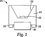
図1はLED20の一実施形態の概略断面図である。LED20は反射性基板25を含むLED本体24内に載置されたダイ22を含む。またLED10は、両方ともダイ22に電気的に接続された第1の電極26および第2の電極28、ならびにポスト30を含む。
FIG. 1 is a schematic cross-sectional view of an embodiment of an
本明細書に用いられるように、用語「LED」および「発光ダイオード」は一般に、ダイオードに電力を供給するコンタクト領域を有する発光半導体要素を指している。無機半導体発光ダイオードの異なる形状を、例えば1つまたは複数のIII族要素、および1つまたは複数のV族要素の組み合わせ(III−V族半導体)で形成し得る。LED内で用いることができるIII−V族半導体材料の例には、窒化ガリウムまたは窒化インジウム・ガリウムなどの窒化物、およびリン化インジウム・ガリウムなどのリン化物がある。他のタイプのIII−V族材料も、周期表の他の族の無機材料と同様に用いることができる。 As used herein, the terms “LED” and “light emitting diode” generally refer to a light emitting semiconductor element having a contact region that provides power to the diode. Different shapes of inorganic semiconductor light emitting diodes may be formed, for example, with one or more group III elements and a combination of one or more group V elements (III-V semiconductors). Examples of III-V semiconductor materials that can be used in LEDs include nitrides such as gallium nitride or indium gallium nitride, and phosphides such as indium gallium phosphide. Other types of III-V materials can be used as well as inorganic materials of other groups of the periodic table.
LEDは例えばLEDダイ、表面実装LED、チップオンボードLED、および他の構成のLEDを始めとする、パッケージ化または非パッケージ化形状であり得る。チップオンボード(COB)は回路基板上に直接実装されたLEDダイ(すなわち未パッケージ化LED)を指す。また用語LEDはパッケージ化、またはLEDから放射された光を異なる波長の光に変換する蛍光体に関連したLEDを含む。ワイヤボンディング、オートメーション化ボンディング(TAB)、またはフリップチップ・ボンディングによりLEDへの電気的接続を行うことができる。LEDは図に概略的に示されているとともに、本明細書に説明するように未パッケージ化LEDダイまたはパッケージ化LEDであり得る。 The LEDs can be packaged or unpackaged shapes including, for example, LED dies, surface mount LEDs, chip on board LEDs, and other configurations of LEDs. Chip on board (COB) refers to an LED die (ie, unpackaged LED) mounted directly on a circuit board. The term LED also includes LEDs associated with phosphors that package or convert light emitted from the LED into light of a different wavelength. Electrical connections to the LEDs can be made by wire bonding, automated bonding (TAB), or flip chip bonding. The LEDs are shown schematically in the figure and can be unpackaged LED dies or packaged LEDs as described herein.
LEDは米国特許第5,998,935号明細書(清水ら)に記載されているような天面発光であり得る。代替的にはLEDは米国特許公報第2004/0,233,665A1号明細書(ウェスト(West)ら)に記載されているような側面発光であり得る。 The LED can be top emitting as described in US Pat. No. 5,998,935 (Shimizu et al.). Alternatively, the LED can be side emitting as described in US Patent Publication No. 2004 / 0,233,665 A1 (West et al.).
赤色、緑色、青色、紫色、または赤外スペクトル領域などの任意の波長で発光するようにLEDを選択することができる。一連のLED内でLEDは各々同じスペクトル領域で発光することが可能であり、または異なるスペクトル領域で発光することが可能である。異なるLEDを用いて異なる色を生成してもよく、発光素子から放射された光の色が選択可能である。異なるLEDの個々の制御は放射光の色を制御する能力につながる。加えて白色光が望ましい場合には、異なる色の光を放射する多数のLEDを設けてもよく、その複合効果は視認者により白色であると知覚される光を放射することである。白色光を生成する他の手法は、比較的短い波長の光を放射する1つまたは複数のLEDを用いるとともに、蛍光波長変換器を用いて放射光を白色光に変換することである。白色光は人間の目の蛍光体を刺激して、普通の観察者が「白色」と考え得る外観を生じる光である。そのような白色光は赤色(一般に暖かい白色光と称される)へ、または青色(一般的に冷たい白色光と称される)へバイアスされ得る。そのような光は100までの演色評価数を有することができる。 The LEDs can be selected to emit at any wavelength, such as red, green, blue, purple, or infrared spectral regions. Within a series of LEDs, each LED can emit in the same spectral region, or it can emit in a different spectral region. Different LEDs may be used to generate different colors, and the color of light emitted from the light emitting elements can be selected. Individual control of different LEDs leads to the ability to control the color of the emitted light. In addition, if white light is desired, multiple LEDs that emit light of different colors may be provided, and the combined effect is to emit light that is perceived as white by the viewer. Another approach to generating white light is to use one or more LEDs that emit light of a relatively short wavelength and convert the emitted light to white light using a fluorescence wavelength converter. White light is light that stimulates the phosphor of the human eye and produces an appearance that a normal observer can think of as “white”. Such white light can be biased to red (commonly referred to as warm white light) or blue (commonly referred to as cold white light). Such light can have a color rendering index of up to 100.
図1のLED20は任意の適当なLEDダイ22を含み得る。例えばLEDダイ22は個別のpおよびnドープ半導体層、基板層、バッファ層、および上層とを含み得る。LEDダイ22の主放射面と、下面と、側面とが単純な矩形配置で示されているが、他の既知の構成、例えば直立または倒立であり得る角錐台形状を形成する傾斜側面も考えられる。LEDダイへの電気コンタクトも簡略化のため示されていないが、既知の通りダイの表面のいずれかの上に設けることができる。
The
LED20は1つのダイ22を有するものとして示されているが、LED20は2つ以上のダイ22、例えば赤色発光ダイ、緑色発光ダイ、および青色発光ダイを含むことができる。いくつかの実施形態においてLEDダイ22は、両方の電気コンタクトがダイ22の下面にあるフリップチップ設計であり得る。そのような実施形態において任意の適当な技術を用いて、ダイ22をLED20の第1および第2の電極26、28に電気的に接続し得る。
Although the
代替的実施形態においてLED20は、ワイヤボンドLEDダイ22を含み得る。例えば図2は1ワイヤボンドLEDダイ122を含むLED120の概略断面図である。ダイ122はダイ122の上面に取り付けられたワイヤ127を介して第1の電極126に電気的に接続されている。ダイ122の下面はLED120の第2の電極128に電気的に接続されている。いくつかの実施形態においてLEDダイ122はダイ122の任意の適当な表面または多数の表面上に、ダイ122を第1および/または第2の電極126、128および/またはポスト130に電気的に接続する、2つ以上のワイヤボンドを有することもできる。任意の適当なワイヤを用いてダイ122を第1の電極126に接続し得る。また任意の適当な技術を用いてワイヤ127をダイ122と第1の電極126とに取り付け得る。またLED120は反射体125を含むLED本体124と、ポスト130とを含む。図1に図示された実施形態のLEDダイ22、本体24、第1および第2の電極26、28、ならびにポスト30に対して本明細書で述べた設計上の考慮および可能性のすべては、図2に図示された実施形態のLEDダイ122、本体124、第1および第2の電極126、128、ならびにポスト130に同等に適用される。
In an alternative embodiment, the
図1に戻るとLED本体24は、LEDダイ22からの縁部放射光を捕獲するとともにそれを前方に屈曲する反射面25を含む。任意の適当な材料、例えば金属、高分子等を用いてLED本体24を形成し得る。反射面25は鏡面または拡散反射性であり得る。いくつかの実施形態において反射面25は、ミネソタ州セントポール(St.Paul,Minnesota)のスリーエム・カンパニー(3M Company)から入手可能なビキュイティ(登録商標)イー・エス・アール(Vikui(登録商標)ESR)フィルムなどの多層高分子反射フィルムを含み得る。
Returning to FIG. 1, the
またLED20はLEDダイ22に熱的に接続されたポスト30を含む。ポスト30は、熱がダイ22から且つLED20の外に向けられるように低熱抵抗経路として動作することができる。ポスト30はダイ22と接していてもよい。代替的にはポスト30は熱伝導接着剤または他の材料によりダイ22に熱接続され得る。
The
任意の適当な材料を用いてポスト30を形成し得る。いくつかの実施形態においてポスト30は熱伝導性材料、例えば銅、ニッケル、金、アルミニウム、スズ、鉛、銀、インジウム、酸化亜鉛、酸化ベリリウム、酸化アルミニウム、サファイア、ダイヤモンド、窒化アルミニウム、炭化シリコン、グラファイト、マグネシウム、タングステン、モリブデン、シリコン、高分子バインダ、無機バインダ、ガラスバインダ、およびそれらの組み合わせを含む。またポスト30は高い熱伝導率用作動流体も含み得る。ポスト30はそのため、流体輸送が毛細管流動または2相液体/沸騰システムによるヒートパイプと考えられる。またいくつかの実施形態においてポスト30は導電性であり得る。任意の適当な導電性材料、例えば銅、ニッケル、金、アルミニウム。スズ、鉛、銀、インジウム、およびそれらの組み合わせを用いて導電性ポスト30を形成し得る。一実施形態においてポスト30は熱的および電気的両方で伝導性であり得る。
Any suitable material can be used to form
またポスト30の部分の電気的絶縁を提供するように導電性ポスト30を区分することができる。このような区分が縦方向に行われ、各区分が良好な熱伝導率を有することが好ましい場合がある。例えば円柱状ポストを熱的および電気的伝導性材料、例えばアルミニウムの2つの半円柱で構成することも可能であり、それらの間に誘電体層または領域が介在して長さに沿って高熱伝導性ポストを形成するが、ポストの直径にわたって比較的限定された熱伝導性を有するとともにポストの直径にわたって電導性のない状態で互いに積層されている。ポストの3つ以上の区分も可能である。
Also, the
ポスト30は任意の適当なサイズまたは形状を取ることができる。いくつかの実施形態においてポスト30は円柱形状を取ることができる。代替的にはポスト30は先細形状をとることができる。またいくつかの実施形態においてポスト30は、本明細書にさらに説明するように1つまたは複数のスレッドを含み得る。ポスト30は単一のポストまたは一体の本体を含んで示されているが、ポスト30は2つ以上のポストを含むことが可能であり、各々熱伝導性基板12と接している。いくつかの実施形態においてポスト30は、LED20を基板に実装する助けとなり得る1つまたは複数の隆起を含み得る。
The
LED本体24は任意の適当な技術、例えば接着、ボンディング、溶接等を用いて恒久的にポスト30に取り付け得る。いくつかの実施形態においてポスト30はLED本体24と一体であり得る。代替的にはLED本体24はポスト30に取り外し可能に取り付け得る。任意の適当な技術を用いてLED本体24をポスト30に取り外し可能に取り付け得る。例えばポスト30は1つまたは複数のスレッドを含み得るとともに、LED本体24も本体24がポスト30上にねじ止めされ得るように1つまたは複数のスレッドを含み得る。代替的にはLED本体24はポスト30に摩擦嵌合され得る。
The
一般に従来の回路基板およびフィルムを用いてLEDを電源および基板に接続することができる。LEDはほとんどの他の電子構成要素と同じ要件の多くを共有するが、相違がある。第1にLEDは高価であるとともに、LEDを用いた点灯システムを構築するための最も費用効果のある設計はヒートシンク熱抵抗への強い接合を有する場合があり、LEDの熱劣化を増大する恐れがある。第2にLEDは光学キャビティを照明することが多く、そこで光は回路基板で何回か反射される。 In general, conventional circuit boards and films can be used to connect the LEDs to the power source and the board. LEDs share many of the same requirements as most other electronic components, but there are differences. First, LEDs are expensive, and the most cost-effective design for building lighting systems using LEDs may have a strong bond to the heat sink thermal resistance, which can increase the thermal degradation of the LED. is there. Second, LEDs often illuminate the optical cavity, where the light is reflected several times at the circuit board.
アセンブリ内の光吸収の防止を助けるために、回路基板を高反射性コーティング、例えばチタニア充填コーティングまたは反射フィルムで被覆することにより回路基板を製造し得る。しかしこれらのタイプのコーティングは両方とも、LEDがコーティングを介して回路基板と電気的および熱的接触を行うようにパターニングする必要がある。反射コーティングまたはフィルムのこのパターニングは高価である恐れがあるとともに、LEDから回路基板への良好な熱伝導性を提供しない場合がある。 To help prevent light absorption in the assembly, the circuit board may be manufactured by coating the circuit board with a highly reflective coating, such as a titania-filled coating or a reflective film. However, both of these types of coatings need to be patterned so that the LED makes electrical and thermal contact with the circuit board through the coating. This patterning of the reflective coating or film can be expensive and may not provide good thermal conductivity from the LED to the circuit board.
代替的回路基板は、回路へのLEDの実装が回路基板との良好な熱的接触も行うとともに反射体をパターニングするものでもある。 An alternative circuit board is one in which mounting the LEDs on the circuit also provides good thermal contact with the circuit board and patterns the reflector.
一般に多数の適当な技術、例えば超音波溶接、RF溶接、サーモソニック溶接、圧入、貫通、ねじ止め等を用いて、本開示のLEDを基板に取り付けることができる。このようなLEDは様々な基板に迅速且つ容易に取り付けられるように設計されている。 In general, a number of suitable techniques, such as ultrasonic welding, RF welding, thermosonic welding, press fitting, penetration, screwing, etc. can be used to attach the LED of the present disclosure to the substrate. Such LEDs are designed to be quickly and easily attached to various substrates.
例えば図3は照明アセンブリ200の一実施形態の概略断面図である。アセンブリ200は熱伝導性基板212と、少なくとも1つのアパーチャ248を含む反射層240とを含む。反射層240は熱伝導性基板212の第1の主面214に近接配置されている。またアセンブリ200は反射層240と第1の主面214との間に配置されたパターン化導電層250と、少なくとも1つのLED220とを含む。アセンブリ200は少なくとも1つのアパーチャ249を有する支持層242をさらに含む。
For example, FIG. 3 is a schematic cross-sectional view of one embodiment of a
熱伝導性基板212は第1の主面214と第2の主面215とを含む。基板212は熱伝導性である任意の適当な材料、例えば銅、ニッケル、金、アルミニウム、スズ、鉛、銀、インジウム、酸化亜鉛、酸化ベリリウム、酸化アルミニウム、サファイア、ダイヤモンド、窒化アルミニウム、炭化シリコン、グラファイト、マグネシウム、タングステン、モリブデン、シリコン、高分子バインダ、無機バインダ、ガラスバインダ、導電性でもあってもなくてもよい熱伝導性粒子が充填されたポリマー類、毛細管流動ヒートパイプ、2相熱輸送デバイス、およびそれらの組み合わせを含み得る。いくつかの実施形態において基板212は他の材料に溶接可能(例えば超音波溶接可能)、例えばアルミニウム、銅、金属被覆セラミックまたはポリマー、もしくは熱伝導性充填ポリマーに溶接可能であり得る。基板212は任意の適当なサイズおよび形状を含み得る。
Thermally
いくつかの実施形態において熱伝導性基板212は導電性でもあり得る。このような導電性基板は任意の適当な導電性材料、例えば銅、ニッケル、金、アルミニウム、スズ、鉛、銀、インジウム、およびそれらの組み合わせを含み得る。
In some embodiments, the thermally
熱伝導性基板212は、例えばLED220への電気的接続を行うこと、LED220からの直接的熱経路を提供すること、LED220から横方向の熱拡散を提供すること、および他のシステムへの電気接続を提供することを始めとする目的の組み合わせを果たすことができる。
The thermally
いくつかの実施形態において熱伝導性基板212は可撓性であり得る。そのような実施形態において反射層240およびパターン化導電層240も可撓性であることが好ましい場合がある。銅導電層が上にあるポリイミド絶縁基板を有する適当な可撓性材料は、スリーエム・カンパニー(3M Company)から入手可能なスリーエム(登録商標)フレキシブル・サーキット(3M(登録商標) Flexible Circuits)である。
In some embodiments, the thermally
熱伝導性基板212は全体として熱伝導性基板を提供する一体の材料、または代替的には1つまたは複数の材料層であり得る。いくつかの実施形態において熱伝導性基板212は、表面積の増加により熱散逸性の増加を提供する、基板212を貫通して形成されたタブまたはフィンを含み得る。他の実施形態において熱伝導性基板212の第1および/または第2の主面214、215は、エッチングまたは溝を設けることによっても、冷却用のより大きい表面積を提供し得る。タブを熱伝導性基板212の第2の主面216から延びるように基板212内に形成することができる。このようなタブは熱伝導性基板212の対流冷却効率を増加させることができるとともに、LED間の熱伝達を低減することもできる。
The thermally
熱伝導性基板212の第1の主面214に近接しているのは反射層240である。図示の実施形態において反射層240は支持層242の第1の主面244上に位置している。一般に少なくとも1つのLED220により放射された光の少なくとも一部分が、反射層240で反射されて基板212から離れるように向けられ得る。反射層240が入射する光の少なくとも80%を反射することが望ましい場合がある。反射層240が入射する光の少なくとも95%を反射することがより好ましい場合がある。反射層240が入射する光の少なくとも99%を反射することがさらに好ましい場合がある。反射層240は鏡面または拡散反射性であり得る。
Close to the first
反射層240は反射層240を貫通して延びる少なくとも1つのアパーチャ248を含む。反射層240の少なくとも1つのアパーチャ248は、本明細書でさらに説明するようにLED220が熱伝導性基板212に熱的に、およびいくつかの実施形態において電気的に接続され得るように、支持層242の少なくとも1つのアパーチャ249と実質的に位置合わせされている。
The
反射層240は任意の適当な反射材料、例えば金属、高分子等を含み得る。例えば反射層240はアルミニウム、銅、銀、またはそれらの組み合わせを含み得る。
The
いくつかの実施形態において反射層240は金属と誘電材料との組み合わせを含み、その組み合わせが非導電性、例えば銀またはアルミニウムとポリマーまたは無機酸化物との組み合わせであり得る。金属と誘電材料との他のそのような適当な組み合わせには、ガラス、無機酸化物、ポリエチレンテレフタレート、ポリエチレンナフタレートなどの縮合重合体、ポリオレフィン類およびポリフルオロポリマー類などの飽和重合体、ならびにエポキシ類、ポリスチレン、ポリカーボネート、ポリシロキサン類、ポリビニルスチレン類、ポリアクリレート類等を始めとする他のポリマー類で作製された、誘電材料の層または連続マトリクス内に被覆された、銀、銅、アルミニウム、スズ、インジウムおよび金で作製された1つまたは複数の導電性粒子、ファイバ、または他の物体がある。
In some embodiments, the
またいくつかの実施形態において反射層240は、変動屈折率の多数のポリマー層を有するフィルム、例えば米国特許第5,882,774号明細書(ジョンザ(Jonza)ら)、米国特許第6,080,467号明細書(ウェーバー(Weber)ら)、および米国特許第6,531,230B1号明細書(ウェーバー(Weber)ら)に記載されているフィルムを含む。
Also, in some embodiments, the
拡散反射の場合、反射層240は拡散反射粒子、例えば二酸化チタン粒子を含むマトリクスなどの白色拡散反射体でもよい。いくつかの実施形態において拡散反射層240は充填ポリマーを含むことができる。一般に充填ポリマーおよび塗料は有機樹脂またはバインダを含むとともに、通例チタニアまたは硫酸バリウムなどの適当な無機粒子を充填することにより不透明化されている。また拡散反射層240は塗料、エナメル、無機粉体、チタニアなどの高散乱白色粉体、またはポリテトラフルオロエチレン(PTFE)を含むことができる。例えばエナメルは支持層242上に(例えば電気泳動)塗布されたスラリーまたは粉体として堆積され得る。銅またはアルミニウムなどの熱伝導性材料に適合したこのようなエナメル組成が利用可能である。また例えばPTFEは白色粉体として堆積またはシートとして形成されて、金属基板に積層され得る。反射層240は拡散反射コーティングまたはフィルムが上に形成または取り付けられた鏡面反射基板も含み得る。
In the case of diffuse reflection, the
反射層240は、例えば粘着剤を用いて支持層242の第1の主面244に取り付けることができる。代替的には任意の適当な技術、例えば化学蒸着、プラズマ蒸着、スパッタリング、および蒸着コーティングを用いて反射層240を第1の主面244上に形成し得る。アルミニウムを含む反射層の場合、支持層242への物理的蒸着技術、箔積層、またはめっきを用いてアルミニウムを蒸着し得る。アルミニウムを保護材料、反射率強化層、またはその両方、例えばフッ化マグネシウムで、もしくは陽極酸化処理に続いて熱および/または化学処理により被覆して、酸化アルミニウム層内のいかなる導電性孔も封止し得る。
The
本明細書に述べるように、反射層240は層240を貫通して形成される少なくとも1つのアパーチャ248を含む。いくつかの実施形態において反射層240のアパーチャ248と支持層242のアパーチャ249とは、LED220が熱伝導性基板212に熱的および/または電気的に接続することができるように、LED220と実質的に位置合わせされている。反射層240に含まれる材料のタイプに応じて、任意の適当な技術を用いてアパーチャ248を形成することができる。例えばフォトリソグラフィを用いて、感光性バインダを含む誘電体層内にアパーチャ248を形成することができる。無機粉体をフォトレジスト溶液(例えばポリビニルアルコールと二クロム酸アンモニウムまたは二クロム酸ゼラチンとを含む溶液)内に懸濁させることができる。懸濁液は支持層242上に塗布され、乾燥され、さらにマスクを介して露光される。水で洗浄することによって非露光領域を除去してパターン化コーティングを残す。支持層242に光粘着性コーティングを塗布し、マスクを介してコーティングを露光し、その後粉体を塗布またはまぶすことによって、粉体塗装をフォトリソグラフィによりパターニングすることができる。バインダ内の粉体の吹きつけ塗装も実現可能である。塗布される特徴に位置合わせされたマスクを用いることにより粉体塗装をパターニングすることができる。
As described herein, the
スリーエム・カンパニー(3M Company)から入手可能なビキュイティ(登録商標)イー・エス・アール(Vikuiti(登録商標)ESR)フィルムなどのフィルムまたは積層コーティングを含む反射層240の場合、支持層242への取り付け前に、パンチング、ダイカッティング、レーザドリル、または火炎穿孔によりアパーチャを形成し得る。またフィルムを支持層242に取り付けた後に、パターン化レジスト層を介するエッチングによりそのようなフィルム内にアパーチャを形成し得る。いくつかの実施形態において、本明細書にさらに説明するように取り付けプロセス中にLED220によりアパーチャ248を形成することができる。いくつかの実施形態において反射層240のアパーチャ248および支持層242のアパーチャ249を同時に形成することができる。
In the case of a
図3に図示した照明アセンブリ200は反射層240を含むが、いくつかの実施形態において反射層240が低反射率を呈することが望ましい場合がある。例えば低反射率層は、例えばアクティブ信号用途に用いられる一連の個々にアドレス可能なLEDを含むアセンブリに、より大きいコントラストを提供し得る。明るい外光条件で用いられるそのようなアクティブ信号の場合、特定の波長における低反射率をLED光源の特定の発光波長に合わせて、反射層がそれらの波長で高反射性であるがより広いスペクトルにわたって吸収性があり、それにより光出力の増加をもたらす一方で、層により反射される外光量をなお低減するようにし得る。
Although the
そのような低反射率層に適した材料には、炭素充填ポリマー類、特にポリオレフィン類およびフルオロカーボン類を始めとする低指数ポリマー類、および染料または顔料もしくはその両方で充填されたポリマー類がある。ポリマー表面は反射率を低減するように反射防止性であり得る。適当な反射防止方法は、高低指数材料の適当に設計された層、低指数材料の単一層、アルミニウムの薄いコーティングを加水分解することにより作製されたベーマイト、ゾル−ゲルコーティング、モスアイ形微細構造化コーティング、およびグレーデッド・インデックス・コーティングを始めとする、反射率を低減する当該技術で既知の干渉コーティングである。吸収材料の焼結コーティングも適当である。 Suitable materials for such low reflectivity layers include carbon filled polymers, particularly low index polymers, including polyolefins and fluorocarbons, and polymers filled with dyes and / or pigments. The polymer surface can be antireflective so as to reduce reflectivity. Suitable anti-reflective methods include well-designed layers of high and low index materials, single layers of low index materials, boehmite made by hydrolyzing a thin coating of aluminum, sol-gel coatings, moth-eye microstructures Interference coatings known in the art to reduce reflectivity, including coatings and graded index coatings. A sintered coating of the absorbent material is also suitable.
反射層240と熱伝導性基板212の第1の主面214との間に位置しているのは、パターン化導電層250である。パターン化導電層250は熱伝導性基板212から電気的に絶縁されている。図3に図示した実施形態において、パターン化導電層250は支持層242の第2の主面246上に位置している。パターン化導電層250は導体252を含む。任意の適当な数の導体252をパターン化導電層250内またはから形成し得る。パターン化導電層250は任意の適当な導電性材料を含み得る。そのような適当な材料には純粋な形態または合金の金、銅、アルミニウム、および銀がある。パターン化導電層250の導体252は裸または絶縁ワイヤまたは細片でもよい。
Located between the
ワイヤまたは細片は単一次元配列で配置してもよく、もしくは直交配列または3線制御システムで配置してもよい。直交配列または3線制御システムを用いて、論理信号を個々のLEDに供給し得る。例えばLEDを、LEDが制御信号に応じて所定の光出力を有する、2または3リード線回路から信号および電力を取得する集積回路に電気的に接続し得る。 The wires or strips may be arranged in a single dimensional array, or in an orthogonal array or a three-wire control system. An orthogonal array or a three-wire control system can be used to provide logic signals to the individual LEDs. For example, an LED may be electrically connected to an integrated circuit that obtains signal and power from two or three lead circuits, where the LED has a predetermined light output in response to a control signal.
当該技術で既知の任意の適当な技術、例えば化学エッチング、フォトリソグラフィ、化学蒸着、インクジェット印刷等を用いてパターン化導電層250をパターニングし得る。アセンブリ200が一連のLEDを含む実施形態において、パターン化導電層250をアレイの各LEDが個々にアドレス可能であるようにパターニングし得る。
Patterned
また図3の照明アセンブリ200は、熱伝導性基板212に取り付けられた少なくとも1つのLED220を含む。任意の適当な数のLEDをアセンブリ200内に含むことができる。いくつかの実施形態においてアセンブリ200は一連のLED220を含むことができる。このようなアレイを基板212上に長方形パターンまたは正方形パターンで配列し得る。これは情報ディスプレイ用途において垂直および水平ラインの容易な表示を生じる。しかし長方形または正方形パターンは必須ではなく、LED220をある他のパターンで、例えば六角形パターンで熱伝導性基板212上に配列してもよい。代替的にはLED220を熱伝導性基板212上にランダムに配列することができる。
The
少なくとも1つのLED220は、第1の電極226と第2の電極228とに電気的に接続された少なくとも1つのLEDダイ222を含む。LED220は反射面225を含むLED本体224をさらに含む。LEDダイ222はポスト230に熱的に接続されている。図1に図示された実施形態のLEDダイ22、本体24、第1および第2の電極26、28、ならびにポスト30に対して本明細書で述べた設計上の考慮および可能性のすべては、図3に図示された実施形態のLEDダイ222、本体224、第1および第2の電極226、228、ならびにポスト230に同等に適用される。
The at least one
少なくとも1つのLED220は、反射層240のアパーチャ248および支持層242のアパーチャ249内に位置するポスト230を介して熱伝導性基板212に熱的に接続されている。ポスト230は熱伝導性基板212と直接接触し得る。代替的にはポスト230は熱的に導電性接合材料、例えばアクリレート、スチレン、ビニルスチレン、シラン類、および酸化亜鉛、サファイア、ダイヤモンド、炭化シリコン、または窒化アルミニウムが充填されたエポキシ類などの硬化性ポリマー前駆体を介して基板212に熱的に接続され得る。
At least one
少なくとも1つのLED220は第1の電極226と第2の電極228とを介してパターン化導電層250に電気的に接続されている。任意の適当な技術を用いてLED220をパターン化導電層250と電気的に接続し得る。例えば図示の実施形態において、LED220の第1および第2の電極226、228はコンタクト254を介してパターン化導電層250に電気的に接続されている。このようなコンタクト254は、LED220が基板212に取り付けられた時に第1および第2の電極226、228がコンタクト254との非接合電気接続を保つように、ばね装填され得る。
At least one
少なくとも1つのLED220はポスト230を介して熱伝導性基板212に熱的に接続され得る。任意の適当な技術、例えば超音波溶接、RF溶接、サーモソニック溶接、ボンディング、はんだ付け、レーザ溶接等を用いてLED220を熱伝導性基板212に熱的に接続し得る。例えばLED220を熱伝導性基板212に超音波溶接し得る。超音波溶接は通例熱エネルギーに変換される振動を用いて多数の部分を接合するために用いられる。一般的なタイプの超音波溶接はプランジおよび連続溶接、例えば走査または回転溶接である。プランジ溶接では超音波ホーンが突入(部分に向かって進行)して振動を上部に伝達する。連続溶接では超音波ホーンが通例固定であるまたは回転しているとともに、部分がその下方で移動する。超音波溶接のタイプの各々はホーンを含む。
At least one
すべてのホーンはエネルギーを選択波長、周波数および振幅で被溶接部分に付与する。回転ホーンは入力および出力端を有するシャフトと、出力端に載置されているとともに同軸である溶接部とを含む。溶接部の直径は通例シャフトの直径より大きい。溶接部は振動エネルギーの印加で膨張および収縮する直径を有する円筒状溶接面を有する。通例回転ホーンは円筒状であるとともに縦軸を中心に回転する。入力振動は軸方向であり、出力振動は半径方向である。ホーンとアンビルとは互いに接近しているとともに、アンビルはホーンと反対方向に回転することができる。被溶接部分は円筒状面の接線速度に等しい線速度で円筒状面間を通過する。ホーンおよびアンビルの接線速度を材料の線速度と一致させることが、ホーンと材料との間の抗力を最小限に抑える傾向がある。 All horns apply energy to the part to be welded at a selected wavelength, frequency and amplitude. The rotating horn includes a shaft having input and output ends, and a weld that is mounted on the output end and is coaxial. The weld diameter is typically larger than the shaft diameter. The weld has a cylindrical weld surface having a diameter that expands and contracts upon application of vibrational energy. Typically, a rotating horn is cylindrical and rotates about a vertical axis. The input vibration is axial and the output vibration is radial. The horn and anvil are close together and the anvil can rotate in the opposite direction of the horn. The welded parts pass between the cylindrical surfaces at a linear velocity equal to the tangential velocity of the cylindrical surfaces. Matching the tangential velocity of the horn and anvil to the linear velocity of the material tends to minimize drag between the horn and the material.
任意の適当な超音波溶接装置および技術を用いてLED220を熱伝導性基板212に取り付け得る。一般にLED220のポスト230は熱伝導性基板212に近接配置されている。超音波エネルギーは、超音波エネルギーによって生成された熱がポスト230を熱伝導性基板212に付着させるようにLED220に印加される。
The
照明アセンブリが光学キャビティ内または近接して配置されている典型的なバックライト付ディスプレイにおいて、LEDまたは他の光源により放射された光は回路基板で数回反射され得る。このような回路基板は、回路基板上に例えばチタニア充填コーティングまたは反射フィルムを始めとする高反射性コーティングを有して製造され得る。これらのタイプの反射体のいずれも、LEDが回路基板と電気的および熱的接触を行うようにパターニングする必要がある。このパターニングは通例高価であり、さらに回路基板の性質のため、LED接合から基板への熱伝導性がなお悪い場合がある。本開示のアセンブリにおいて反射誘電体層はアパーチャで事前パターニングされている必要はない。 In a typical backlit display where the illumination assembly is located in or close to the optical cavity, the light emitted by the LED or other light source can be reflected several times at the circuit board. Such circuit boards can be manufactured with highly reflective coatings including, for example, titania-filled coatings or reflective films on the circuit board. Both of these types of reflectors need to be patterned so that the LEDs are in electrical and thermal contact with the circuit board. This patterning is typically expensive and, due to the nature of the circuit board, thermal conductivity from the LED junction to the substrate may still be poor. In the assembly of the present disclosure, the reflective dielectric layer need not be pre-patterned with an aperture.
その代わり例えばLED220を基板212に超音波ボンディングするプロセスは、ポスト230が基板212と接触するとともに付着するように、反射層240の一部分を除去することができる。これにより他のタイプの反射層をパターニングすることにより発生するコストを大幅に削減することができる。金などの非酸化材料の薄いコーティングを、ポスト230および熱伝導性基板212の一方または両方の上で用いて、電気的インターフェースの環境安定性を強化することができる。
Instead, for example, the process of ultrasonic bonding the
熱的および電気的伝導性接着剤、はんだリフロー、およびAu/Sn共晶ボンディングは、とりわけLED220を熱伝導性基板212に取り付けるために用いることができる技術である。はんだは通例接着剤より低い熱抵抗を有するが、すべてのLEDがはんだ付け可能ベース金属化を有するわけではない。またはんだ取り付けは、処理中にLEDを位置合わせする溶融はんだの表面張力によるLED自己整合の利点を有する。しかしあるLEDははんだリフロー温度に敏感であり、接着剤がより適当である場合がある。当該技術で既知の低温はんだを、良好な熱伝導性が必要不可欠であるが200℃より高い従来のリフロー温度に耐えられないアセンブリに用いることができる。
Thermal and electrically conductive adhesives, solder reflow, and Au / Sn eutectic bonding are techniques that can be used to attach the
いくつかの実施形態において、少なくとも1つのLED220をポスト230を介して熱伝導性基板212に熱的にも電気的にも接続し得る。換言すればLED222ダイ用の電極の一方または両方はポスト230を介して電気的に接続され得る。このような実施形態において熱伝導性基板212は、基板212に取り付けられた1つまたは複数のLED220に対して共通接続になる。このためLED220から離れるように熱を伝達することに加えて、熱伝導性基板212は照明アセンブリ200の電気回路のアクティブ素子でもあり得る。例えば熱伝導性基板212はアセンブリ200内のLED220の各々に共通電気グランドを提供する。また熱伝導性基板212が良好な導電性を有する材料で構成されている場合、低い電圧降下およびEMIシールディングを有する均等電流分布を始めとするさらなる利点が達成され得る。任意の適当な技術、例えば、照明アセンブリおよびその作製方法(ILLUMINATION ASSEMBLY AND METHOD OF MAKING SAME)、と題された同一人により所有且つ同時係属出願の米国特許出願(米国特許出願第11/018,605号明細書)に記載されている技術を用いて、LEDダイ222の電極の一方または両方をポスト230に電気的に接続することができる。
In some embodiments, at least one
本明細書に述べたように、任意の適当な技術を利用して本開示のLEDを熱伝導性基板に取り付け得る。いくつかの実施形態において、LED本体をポストに取り付ける前にLEDのポストを基板に取り付けるまたは接合することができる。例えばポスト230はLED本体224をポスト230上にねじ込むための1つまたは複数のスレッドを含むことができる。ポスト230への取り付けを容易にするために、LED本体224はポスト230のスレッドと噛合するスレッドも含み得る。
As described herein, any suitable technique may be utilized to attach the LED of the present disclosure to a thermally conductive substrate. In some embodiments, the LED post can be attached or bonded to the substrate prior to attaching the LED body to the post. For example, the
一般に任意の適当な技術、例えば超音波溶接を用いてまずポスト230を基板212に取り付けることによって、少なくとも1つのLED220を熱伝導性基板212に取り付け得る。反射層240がアパーチャ248を含むとともに支持層242がアパーチャ249を含む場合には、ポスト230はアパーチャ248、249を介して基板212と熱的に接続される。他の実施形態においてアパーチャ248、249は取り付けプロセス中に反射層240および支持層242を貫通して形成し得る。ポスト230が基板212に取り付けられた後、LED本体224は任意の適当な技術を用いてポスト230に取り付けられ得る。一実施形態においてLED本体224は、第1の電極226および第2の電極228がコンタクト254を介してパターン化導電層250と電気的に接続されるまで、ポスト230上にねじ込まれる。代替的にはポスト230がスレッドを含まない場合には、LED本体224はポスト230上に摩擦嵌合され得るか、またはLED本体224は保持突起、またはポスト230に取り付けるための当該技術で既知の他の装置を含み得る。
In general, at least one
照明アセンブリ200の支持層242は、反射層240およびパターン化導電層250に支持構造を提供する任意の適当な材料、例えば金属、ポリマー等を含むことができる。いくつかの実施形態において支持層242は、パターン化導電層250が導電性反射層240と電気的に接続しないように、誘電材料を含むことができる。またいくつかの実施形態において支持層242および導電層250は、パターン化導電層250とは反対側の表面244上に位置する反射層240を有する印刷基板(PCB)を含むことができる。
The
支持層242は隔離絶縁器252によって熱伝導性基板212の第1の主面214から分離されている。このような隔離絶縁器252は、支持層242を支持することができるとともにパターン化導電層250を熱伝導性基板212から電気的に絶縁させることが可能な、任意の適当な材料であり得る。いくつかの実施形態において隔離絶縁器216は熱伝導性基板212内に形成することができるとともに、基板212の第1の主面214から延びることができる。任意の適当な技術、例えば刻み付け、エンボス加工、エッチング、研磨等を用いて隔離絶縁器252を形成し得る。
The
一般には任意の適当な技術を用いて図3の照明アセンブリ200を製造し得る。例えば支持層242が熱伝導性基板212の隔離絶縁器216上に配置される前に、パターン化導電層250を支持層242の第2の主面246上に形成し得るとともに、反射層240を支持層242の第1の主面244上に形成し得る。また支持層242の配置前に、少なくとも1つのLED220をパターン化導電層250に電気的に接続し得る。支持層242は隔離絶縁器216とは非接合接触であってもよく、または支持層242を任意の適当な技術、接着、溶接、はんだ付け等を用いて隔離絶縁器216に取り付けてもよい。いくつかの実施形態において支持層242は、隔離絶縁器216のいくつかのまたはすべての一部分が開口内に位置するように、隔離絶縁器216と位置合わせされた開口を含み得る。
In general, any suitable technique may be used to manufacture the
代替的には支持層242およびパターン化導電層250を隔離絶縁器252の上に配置して、その後反射層240を支持層242の第1の主面244上に形成し得る。また支持層242、パターン化導電層250、および反射層240を熱伝導性基板212の第1の主面214に近接配置した後、少なくとも1つのLED220を熱伝導性基板212に取り付け得る。
Alternatively,
本明細書に述べるように、任意の適当な技術を用いて本開示のLEDを熱伝導性基板に取り付け得る。例えばLEDは熱伝導性基板内に埋め込まれた部分を有するポストを含むことができる。例えば図4は照明アセンブリ300の概略断面図である。アセンブリ300は熱伝導性基板312と、熱伝導性基板312の第1の主面314に近接した反射層340と、反射層340と第1の主面314との間に配置されたパターン化導電層350と、少なくとも1つのLED320とを含む。またアセンブリ300は、第1の主面344と、隔離絶縁器316によって熱伝導性基板312の第1の主面314と分離された第2の主面346とを有する支持層342とを含む。反射層340は支持層342の第1の主面344上に配置されている。パターン化導電層350は支持層342の第2の主面346上に配置されている。図3に図示された実施形態の熱伝導性基板212、反射層240、パターン化導電層250、支持層242、および少なくとも1つのLED220に対して本明細書で述べた設計上の考慮および可能性のすべては、図4に図示された実施形態の熱伝導性基板312、反射層340、パターン化導電層350、支持層342、および少なくとも1つのLED320に同等に適用される。
As described herein, any suitable technique may be used to attach the LED of the present disclosure to a thermally conductive substrate. For example, an LED can include a post having a portion embedded in a thermally conductive substrate. For example, FIG. 4 is a schematic cross-sectional view of
少なくとも1つのLED320は、ポスト330と、LEDダイ322と、LED本体324と、反射層325とを含む。またLED320は第1および第2の電極326、328を含む。ポスト330の少なくとも一部分は熱伝導性基板312内に埋め込まれている。いくつかの実施形態においてポスト330は、ポスト330の第1の端332が熱伝導性基板312内に位置するように埋め込まれている。他の実施形態においてポスト330は、図4の実施形態に図示するように第1の端332が熱伝導性基板312の第2の主面315の外にあるように埋め込まれている。ポスト330の少なくとも一部分を熱伝導性基板312内に埋め込むことにより、熱伝導性基板312と接するポスト330の表面積が、ポスト330が単に基板312の第1の主面314と接している場合より大きくなる。この接触の増加により熱導電性を向上させることができる。
At least one
また熱伝導性基板312の第2の主面315を超えて延びるポスト330の一部分は、外気、強制空気、液体冷却または他の適当な熱散逸技術へのさらなる熱散逸を提供することができる。
Also, a portion of the
少なくとも1つのLED320をポスト330を介して熱伝導性基板312に熱的に接続し得る。任意の適当な技術を用いてLED320を熱伝導性基板312に取り付け得る。例えば窪みまたは開口を熱伝導性基板312内に形成して、LED320のポスト330を窪みに圧入することができる。LED320は、ポスト330と基板312との間の摩擦によって熱伝導性基板312に取り付けられた状態を保つ。任意の適当な技術、例えば刻み付け、エンボス加工、エッチング、アブレーティング、パンチング等を用いて基板312内に窪みまたは開口を形成し得る。
At least one
代替的には、最初に基板312内に窪みまたは穴を形成せずにポスト330で基板312を貫通することにより、少なくとも1つのLED320を基板312に取り付けることができる。基板312の貫通を容易にするために、ポスト330は先の尖ったまたは鋭利な第1の端332を含み得る。
Alternatively, at least one
本明細書に述べるように、任意の適当な技術を利用して本開示のLEDを熱伝導性基板に取り付け得る。いくつかの実施形態において、LED本体のないポストを基板に取り付けた後LED本体をポストに取り付けることができる。 As described herein, any suitable technique may be utilized to attach the LED of the present disclosure to a thermally conductive substrate. In some embodiments, the LED body can be attached to the post after the post without the LED body is attached to the substrate.
一般にまず任意の適当な技術、例えば圧入、貫通、ねじ止め等を用いてポスト330を基板312に取り付けることによって、LED320を熱伝導性基板312に取り付け得る。反射層340がアパーチャ348を含むとともに支持層342がアパーチャ349を含む場合には、ポスト330はアパーチャ348、349内に配置されるとともに基板312と熱的に接続される。他の実施形態において本明細書にさらに説明するように、アパーチャ348、349は取り付けプロセス中に反射層340および支持層342を貫通して形成し得る。ポスト330が基板312に取り付けられた後、LED本体324は任意の適当な技術を用いてポスト330に取り付けられ得る。一実施形態においてLED本体324およびポスト330は、第1の電極326および第2の電極328がコンタクト354を介してパターン化導電層350と電気的に接続されるまで、本体324をポスト330上にねじ込むことができるようなスレッドを含む。代替的にはLED本体324はポスト330上に摩擦嵌合され得るか、またはLED本体324は保持突起、または取り付けるための当該技術で既知の他の装置を含み得る。
In general, the
任意の適当な装置または技術を用いてLED320が熱伝導性基板312から外れないようにすることができる。例えばポスト330は、LED320を基板312に固着するのに役立つ1つまたは複数の突起を有することができる。他の実施形態においてポスト330は、照明アセンブリおよびその作製方法(ILLUMINATION ASSEMBLY AND METHOD OF MAKING SAME)、と題された同一人により所有且つ同時係属出願の米国特許出願(米国特許出願第11/018,605号明細書)に記載されているような、LED320を熱伝導性基板312にねじ込むまたはねじ止めするための1つまたは複数のスレッドを有することができる。
Any suitable device or technique can be used to prevent the
いくつかの実施形態において支持層が必要ない場合もある、例えば図5は照明アセンブリ400の他の実施形態の概略断面図である。アセンブリ400は熱伝導性基板412と、熱伝導性基板412の第1の主面414に近接配置された反射層440と、反射層440と第1の主面414との間に配置されたパターン化導電層450と、少なくとも1つのLED420とを含む。図3に図示された実施形態の熱伝導性基板212、反射層240、パターン化導電層250、および少なくとも1つのLED220に対する設計上の考慮のすべては、図5に図示された実施形態の熱伝導性基板412、反射層440、パターン化導電層450、および少なくとも1つのLED220に同等に適用される。
In some embodiments, a support layer may not be required, for example, FIG. 5 is a schematic cross-sectional view of another embodiment of a lighting assembly 400. The assembly 400 includes a thermally
図5においてアセンブリ400は支持層(例えば図3の支持層242)を含まない。その代わり反射層440が、熱伝導性基板412の第1の主面414と反射層440との間に配置されている隔離絶縁器416上に配置されている。反射層440は隔離絶縁器416上に配列され得るか、または反射層440は例えば接着剤を用いて隔離絶縁器に取り付けられ得る。本明細書に説明した任意の適当な反射層を図5のアセンブリ400と共に用い得る。
In FIG. 5, assembly 400 does not include a support layer (eg,
さらに図3の実施形態とは異なり、パターン化導電層450は熱伝導性基板412の第1の主面414上に配置されている。パターン化導電層450が熱伝導性基板412と電気的に接触しないように、パターン化導電層450と熱伝導性基板412との間に誘電体層が必要であり得ることは当業者には理解されよう。任意の適当な誘電体層を利用し得る。また任意の適当な技術、例えば化学蒸着、スパッタリング等を用いてそのような誘電体層を熱伝導性基板412の第1の主面414上に形成し得る。
Further, unlike the embodiment of FIG. 3, the patterned
パターン化導電層450は任意のタイプの導電層、例えば図3のパターン化導電層250であり得る。例えばパターン化導電層450は、熱伝導性基板412の第1の主面414上に配列または取り付けられた金網を含むことができる。
The patterned
いくつかの実施形態において、非導電性である反射層(すなわち誘電体層)の場合、隔離絶縁器416は必要ない場合がある。その代わり反射誘電体層440をパターン化導電層450上に直接配置し得る。
In some embodiments, the
図5に図示した実施形態において、少なくとも1つのLED420は第1および第2の電極426、428を介してパターン化導電層450に電気的に接続されている。このような電極426、428はパターン化導電層450の導体452に電気的に接続されている。任意の適当な技術を用いてLED420をパターン化導電層450に電気的に接続し得る。例えば第1および第2の電極426、428は導体452に超音波接合され得る。代替的にはLED420を、第1および第2の電極426、428が導体452と非接合電気接続の状態であるように、熱伝導性基板412に取り付け得る。他の実施形態において、第1および第2の電極426、428を導体452にはんだ付けし得る。
In the embodiment illustrated in FIG. 5, at least one
任意の適当なLEDを図5のアセンブリ400と共に用い得る。例えばアセンブリ400は、一部が熱伝導性基板412内に埋め込まれたポストを含むLED(例えば図4のLED320)を含むことができる。任意の適当な技術、例えば圧入、貫通、ねじ止め等を用いてそのようなLEDを熱伝導性基板に取り付け得る。またそのようなポストは、図4の実施形態と同様に熱伝導性基板412の第2の主面415を超えて延びる第1の端を有し得る。
Any suitable LED may be used with the assembly 400 of FIG. For example, the assembly 400 can include an LED (eg, LED 320 of FIG. 4) that includes a post partially embedded in a thermally
本開示の照明アセンブリは照明を供給する任意の適当な手法で用いられ得る。例えば本明細書で説明する照明アセンブリのいくつかまたはすべてをディスプレイに照明を提供するために用い得る。図6はディスプレイ装置520に光学的に結合された照明アセンブリ510を含むディスプレイアセンブリ500を概略的に図示する。照明アセンブリ510は本明細書で説明する任意の照明アセンブリ、例えば図3の照明アセンブリ200を含み得る。照明アセンブリ510は照明光をディスプレイ装置520に提供する。ディスプレイ装置520は任意の適当なディスプレイ装置、例えばエレクトロクロミックまたは電気泳動装置、空間光変調器、透過性信号等であり得る。
The illumination assemblies of the present disclosure can be used in any suitable manner for providing illumination. For example, some or all of the lighting assemblies described herein may be used to provide illumination to the display. FIG. 6 schematically illustrates a
例えばディスプレイ装置520は1つまたは複数の空間光変調器を含み得る。いくつかの実施形態において1つまたは複数の空間光変調器は、一連の個々にアドレス可能な制御可能要素を含み得る。このような空間光変調器は適当なタイプの制御可能要素を含み得る。例えば空間光変調器は透過率可変タイプのディスプレイを含み得る。いくつかの実施形態において空間光変調器は、透過型光変調器の一例である液晶ディスプレイ(LCD)を含み得る。いくつかの実施形態において空間光変調器は、反射型光変調器の一例である変形可能ミラーデバイス(DMD)を含み得る。
For example, the
ディスプレイ装置520は、表示画像を生成する任意の適当な光学および非光学素子、例えばレンズ、拡散器、偏光子、フィルタ、ビームスプリッタ、輝度強化フィルム等を含み得る。当該技術で既知の任意の適当な技術を用いて、照明アセンブリ510をディスプレイ装置520に光学的に結合し得る。
いくつかの実施形態において、ディスプレイ装置520は照明アセンブリ510により直接点灯され得る。換言すればディスプレイ装置520を、例えば米国特許公報第2004/0228106号明細書(スティーブンソン(Stevenson)ら)に記載された直接点灯ディスプレイのように、照明アセンブリ510と視認位置との間に配置することが可能である。他の実施形態においてディスプレイ装置520は、照明アセンブリ510によって側面点灯され得る、すなわち照明アセンブリ510からの光は、デバイス520の外面に実質的に直交するディスプレイ装置520の1つまたは複数の側面を介して向けられる。このような側面点灯実施形態には、米国特許公報第2004/0228106号明細書(スティーブンソン(Stevenson)ら)に記載されたシステムがあり得る。
In some embodiments, the
本明細書に引用したすべての参照文献および公報はそれら全体を本開示に明確に参照により援用する。本開示の例示的実施形態を説明するとともに、本開示の範囲内の可能な変更例を参照した。開示のこれらのおよび他の変形例ならびに変更例は、開示の範囲から逸脱することなく当業者には明らかであろうとともに、本開示は本明細書に記載された例示的実施形態に限定されないことは理解できよう。したがって開示は冒頭に記載の特許請求の範囲によってのみ限定されるものである。 All references and publications cited herein are hereby expressly incorporated by reference into the present disclosure in their entirety. While describing exemplary embodiments of the present disclosure, reference has been made to possible variations within the scope of the present disclosure. These and other variations and modifications of the disclosure will be apparent to those skilled in the art without departing from the scope of the disclosure, and the disclosure is not limited to the exemplary embodiments described herein. Can understand. Accordingly, the disclosure is limited only by the following claims.
Claims (3)
前記熱伝導性基板の前記第1の主面に近接する、支持層上の反射層であって、前記支持層が前記熱伝導性基板と前記反射層との間に位置する、反射層と、
前記反射層と前記熱伝導性基板の前記第1の主面との間に配置されているとともに、前記熱伝導性基板から電気的に絶縁されているパターン化導電層と、
前記熱伝導性基板に取り付けられたポストを備える少なくとも1つのLEDとを備え、
前記少なくとも1つのLEDが、前記ポストを介して前記熱伝導性基板に熱的に接続されているとともに前記パターン化導電層に電気的に接続されている照明アセンブリ。A thermally conductive substrate comprising a first major surface;
A reflective layer on a support layer proximate to the first major surface of the thermally conductive substrate, wherein the support layer is located between the thermally conductive substrate and the reflective layer ;
A patterned conductive layer disposed between the reflective layer and the first major surface of the thermally conductive substrate and electrically insulated from the thermally conductive substrate;
And at least one LED comprising a post attached to the thermally conductive substrate,
The lighting assembly, wherein the at least one LED is thermally connected to the thermally conductive substrate through the post and electrically connected to the patterned conductive layer.
パターン化導電層を、前記パターン化導電層が前記熱伝導性基板から電気的に絶縁されるように、前記熱伝導性基板の前記第1の主面に近接する支持層上に配置し、
反射層を、前記パターン化導電層が前記反射層と前記第1の主面との間にあるように配置し、
ポストを備える少なくとも1つのLEDを設け、
前記少なくとも1つのLEDが前記反射層に隣接するように、前記少なくとも1つのLEDを前記熱伝導性基板に取り付けることとを含み、
前記少なくとも1つのLEDが、前記ポストを介して前記熱伝導性基板に熱的に接続されているとともに前記パターン化導電層に電気的に接続されている、照明アセンブリの作製方法。Providing a thermally conductive substrate comprising a first major surface;
A patterned conductive layer is disposed on a support layer proximate to the first major surface of the thermally conductive substrate such that the patterned conductive layer is electrically isolated from the thermally conductive substrate;
Arranging a reflective layer such that the patterned conductive layer is between the reflective layer and the first major surface;
Providing at least one LED with a post;
Attaching the at least one LED to the thermally conductive substrate such that the at least one LED is adjacent to the reflective layer;
A method of making a lighting assembly, wherein the at least one LED is thermally connected to the thermally conductive substrate through the post and electrically connected to the patterned conductive layer.
前記熱伝導性基板の前記第1の主面に近接する、支持層上の反射層であって、前記支持層が前記熱伝導性基板と前記反射層との間に位置する、反射層と、
前記反射層と前記熱伝導性基板の前記第1の主面との間に配置されているとともに、前記熱伝導性基板から電気的に絶縁されているパターン化導電層と、
前記熱伝導性基板に取り付けられたポストを備える少なくとも1つのLEDとを備え、
前記少なくとも1つのLEDが、前記ポストを介して前記熱伝導性基板に熱的に接続されているとともに前記パターン化導電層に電気的に接続されている、照明アセンブリと、
前記照明アセンブリに光学的に結合され、前記照明アセンブリからの光の少なくとも一部分を変調するように動作可能な複数の制御可能要素を備える空間光変調器とを備えるディスプレイ。A thermally conductive substrate comprising a first major surface;
A reflective layer on a support layer proximate to the first major surface of the thermally conductive substrate, wherein the support layer is located between the thermally conductive substrate and the reflective layer ;
A patterned conductive layer disposed between the reflective layer and the first major surface of the thermally conductive substrate and electrically insulated from the thermally conductive substrate;
And at least one LED comprising a post attached to the thermally conductive substrate,
A lighting assembly, wherein the at least one LED is thermally connected to the thermally conductive substrate through the post and electrically connected to the patterned conductive layer;
A spatial light modulator comprising a plurality of controllable elements optically coupled to the lighting assembly and operable to modulate at least a portion of the light from the lighting assembly.
Applications Claiming Priority (3)
| Application Number | Priority Date | Filing Date | Title |
|---|---|---|---|
| US11/018,961 | 2004-12-21 | ||
| US11/018,961 US7296916B2 (en) | 2004-12-21 | 2004-12-21 | Illumination assembly and method of making same |
| PCT/US2005/042640 WO2006068762A2 (en) | 2004-12-21 | 2005-11-23 | Illumination assembly and method of making same |
Publications (3)
| Publication Number | Publication Date |
|---|---|
| JP2008524826A JP2008524826A (en) | 2008-07-10 |
| JP2008524826A5 JP2008524826A5 (en) | 2009-01-15 |
| JP4728346B2 true JP4728346B2 (en) | 2011-07-20 |
Family
ID=36594551
Family Applications (1)
| Application Number | Title | Priority Date | Filing Date |
|---|---|---|---|
| JP2007548235A Expired - Fee Related JP4728346B2 (en) | 2004-12-21 | 2005-11-23 | Lighting assembly and method of making the same |
Country Status (7)
| Country | Link |
|---|---|
| US (1) | US7296916B2 (en) |
| EP (1) | EP1829125A2 (en) |
| JP (1) | JP4728346B2 (en) |
| KR (1) | KR20070089183A (en) |
| CN (1) | CN100530717C (en) |
| TW (1) | TW200627022A (en) |
| WO (1) | WO2006068762A2 (en) |
Families Citing this family (64)
| Publication number | Priority date | Publication date | Assignee | Title |
|---|---|---|---|---|
| FR2862424B1 (en) * | 2003-11-18 | 2006-10-20 | Valeo Electronique Sys Liaison | DEVICE FOR COOLING AN ELECTRICAL COMPONENT AND METHOD FOR MANUFACTURING THE SAME |
| JP4176703B2 (en) * | 2004-11-25 | 2008-11-05 | 松下電器産業株式会社 | Semiconductor light emitting device, lighting device, portable communication device, camera, and manufacturing method |
| US7285802B2 (en) * | 2004-12-21 | 2007-10-23 | 3M Innovative Properties Company | Illumination assembly and method of making same |
| US7633177B2 (en) * | 2005-04-14 | 2009-12-15 | Natural Forces, Llc | Reduced friction wind turbine apparatus and method |
| US7815355B2 (en) * | 2005-08-27 | 2010-10-19 | 3M Innovative Properties Company | Direct-lit backlight having light recycling cavity with concave transflector |
| US20070047228A1 (en) * | 2005-08-27 | 2007-03-01 | 3M Innovative Properties Company | Methods of forming direct-lit backlights having light recycling cavity with concave transflector |
| US7537374B2 (en) * | 2005-08-27 | 2009-05-26 | 3M Innovative Properties Company | Edge-lit backlight having light recycling cavity with concave transflector |
| KR101298786B1 (en) * | 2005-08-27 | 2013-08-22 | 쓰리엠 이노베이티브 프로퍼티즈 컴파니 | Illumination assembly and system |
| US7943946B2 (en) * | 2005-11-21 | 2011-05-17 | Sharp Kabushiki Kaisha | Light emitting device |
| JP4798432B2 (en) * | 2005-11-21 | 2011-10-19 | ミネベア株式会社 | Surface lighting device |
| US8044412B2 (en) | 2006-01-20 | 2011-10-25 | Taiwan Semiconductor Manufacturing Company, Ltd | Package for a light emitting element |
| US7488097B2 (en) * | 2006-02-21 | 2009-02-10 | Cml Innovative Technologies, Inc. | LED lamp module |
| JP2008034622A (en) * | 2006-07-28 | 2008-02-14 | Sharp Corp | Semiconductor light-emitting element assembly |
| KR101488042B1 (en) | 2007-05-20 | 2015-01-29 | 쓰리엠 이노베이티브 프로퍼티즈 컴파니 | Design parameters for thin hollow cavity backlights of the light-recycling type |
| WO2008144650A1 (en) | 2007-05-20 | 2008-11-27 | 3M Innovative Properties Company | Collimating light injectors for edge-lit backlights |
| TWI467283B (en) | 2007-05-20 | 2015-01-01 | 3M Innovative Properties Co | Recycling backlights with semi-specular components |
| EP2535766A3 (en) | 2007-05-20 | 2013-05-01 | 3M Innovative Properties Company | Asymmetric reflective film and backlight having a hollow cavity, which recycles the light |
| CN101378613B (en) * | 2007-08-27 | 2012-07-04 | 佶益投资股份有限公司 | LED light source and LED lamp body |
| JP2009088373A (en) * | 2007-10-02 | 2009-04-23 | Toyoda Gosei Co Ltd | Led lamp module |
| JP2011519148A (en) * | 2007-12-13 | 2011-06-30 | コーニンクレッカ フィリップス エレクトロニクス エヌ ヴィ | Light emitting diode attached to heat sink |
| JP5702151B2 (en) | 2008-02-07 | 2015-04-15 | スリーエム イノベイティブ プロパティズ カンパニー | Hollow backlight with structured film |
| JP5104385B2 (en) * | 2008-02-20 | 2012-12-19 | 豊田合成株式会社 | LED lamp module |
| US9541698B2 (en) | 2008-02-22 | 2017-01-10 | 3M Innovative Properties Company | Backlights having selected output light flux distributions and display systems using same |
| JP5185683B2 (en) * | 2008-04-24 | 2013-04-17 | パナソニック株式会社 | LED module manufacturing method and lighting apparatus manufacturing method |
| EP2297607B1 (en) | 2008-06-04 | 2014-04-23 | 3M Innovative Properties Company | Hollow backlight with tilted light source |
| US7952114B2 (en) * | 2008-09-23 | 2011-05-31 | Tyco Electronics Corporation | LED interconnect assembly |
| US8220980B2 (en) * | 2008-09-23 | 2012-07-17 | Tyco Electronics Corporation | Socket assembly for light-emitting devices |
| JP5245980B2 (en) * | 2008-09-30 | 2013-07-24 | 豊田合成株式会社 | Light emitting device and manufacturing method thereof |
| JP5440064B2 (en) | 2008-10-21 | 2014-03-12 | 東芝ライテック株式会社 | Lighting device |
| BRPI0914366A2 (en) | 2008-10-27 | 2015-10-20 | 3M Innovative Properties Co | '' backlight equipment '' |
| JP5327601B2 (en) | 2008-12-12 | 2013-10-30 | 東芝ライテック株式会社 | Light emitting module and lighting device |
| US8408724B2 (en) | 2008-12-26 | 2013-04-02 | Toshiba Lighting & Technology Corporation | Light source module and lighting apparatus |
| KR20110134498A (en) * | 2009-03-31 | 2011-12-14 | 코닌클리즈케 필립스 일렉트로닉스 엔.브이. | Led collimation optics module providing an isolation fitting |
| US8192048B2 (en) * | 2009-04-22 | 2012-06-05 | 3M Innovative Properties Company | Lighting assemblies and systems |
| US20100302789A1 (en) * | 2009-05-28 | 2010-12-02 | Qing Li | LED Light Source Module and Method for Producing the Same |
| US9303861B2 (en) | 2009-09-14 | 2016-04-05 | Us Vaopto, Inc. | Light emitting diode light source modules |
| IT1397380B1 (en) | 2010-01-08 | 2013-01-10 | Khatod Optoelectronic Srl | LIGHTING SYSTEM AND ASSEMBLY METHOD OF THE SAME. |
| WO2011082497A1 (en) * | 2010-01-11 | 2011-07-14 | Cooledge Lighting Inc. | Package for light emitting and receiving devices |
| US8820950B2 (en) | 2010-03-12 | 2014-09-02 | Toshiba Lighting & Technology Corporation | Light emitting device and illumination apparatus |
| JP2011238367A (en) * | 2010-05-06 | 2011-11-24 | Funai Electric Co Ltd | Light source mounting structure of plane light-emitting device |
| WO2011142145A1 (en) * | 2010-05-10 | 2011-11-17 | シャープ株式会社 | Light source, light source device, and display device |
| WO2011152133A1 (en) * | 2010-06-02 | 2011-12-08 | シャープ株式会社 | Lighting device, display device, and television receiving device |
| JP5456077B2 (en) | 2011-03-11 | 2014-03-26 | ソウル セミコンダクター カンパニー リミテッド | LED module, manufacturing method thereof, and LED channel letter including LED module |
| US10074779B2 (en) | 2011-03-11 | 2018-09-11 | Seoul Semiconductor Co., Ltd. | LED module, method for manufacturing the same, and LED channel letter including the same |
| TW201250159A (en) * | 2011-06-01 | 2012-12-16 | gui-fang Chen | Light-emitting diode module |
| US9236547B2 (en) | 2011-08-17 | 2016-01-12 | 3M Innovative Properties Company | Two part flexible light emitting semiconductor device |
| US20120175667A1 (en) | 2011-10-03 | 2012-07-12 | Golle Aaron J | Led light disposed on a flexible substrate and connected with a printed 3d conductor |
| US8632221B2 (en) * | 2011-11-01 | 2014-01-21 | Taiwan Semiconductor Manufacturing Company, Ltd. | LED module and method of bonding thereof |
| TWI536617B (en) * | 2012-02-17 | 2016-06-01 | 鴻海精密工業股份有限公司 | Light emitting diode lightbar and method for manufacturing the same |
| WO2013133725A1 (en) | 2012-03-09 | 2013-09-12 | Rawle Christopher Bruce | Portable device for detecting molecule(s) |
| EP2852975B1 (en) * | 2012-05-23 | 2020-04-29 | Lumileds Holding B.V. | Surface mountable semiconductor device |
| DE102012106982A1 (en) | 2012-07-31 | 2014-02-06 | Osram Opto Semiconductors Gmbh | Process for the production of a light source |
| CN102833986B (en) * | 2012-08-16 | 2014-12-31 | 苏州金科信汇光电科技有限公司 | Flexible self-adhesive heat-conduction substrate |
| WO2014137228A1 (en) * | 2013-03-08 | 2014-09-12 | Otago Innovation Limited | Reaction vessel holder and molecule detection device |
| US20140264423A1 (en) * | 2013-03-15 | 2014-09-18 | Grote Industries, Llc | Flexible lighting device including a protective conformal coating |
| CN104100933B (en) * | 2013-04-04 | 2016-08-10 | 深圳市绎立锐光科技开发有限公司 | A kind of Wavelength converter and preparation method thereof, related lighting fixtures |
| WO2014180718A1 (en) * | 2013-05-07 | 2014-11-13 | Koninklijke Philips N.V. | Optical system providing polarized light |
| CN103617969B (en) * | 2013-12-04 | 2016-06-29 | 广州先艺电子科技有限公司 | A kind of weld the heat sink and preparation method thereof of gold-tin alloy thin film |
| US10718474B1 (en) | 2014-11-20 | 2020-07-21 | The Light Source, Inc. | Lighting fixture with closely-packed LED components |
| CN104848067B (en) * | 2015-05-28 | 2017-01-25 | 成都斯科泰科技有限公司 | Multi-core array integrated structure for LED light source |
| US9659844B2 (en) * | 2015-08-31 | 2017-05-23 | Texas Instruments Incorporated | Semiconductor die substrate with integral heat sink |
| CN108954039B (en) * | 2017-05-19 | 2020-07-03 | 深圳光峰科技股份有限公司 | Wavelength conversion device and preparation method thereof |
| KR20210108124A (en) * | 2020-02-25 | 2021-09-02 | 삼성전자주식회사 | Display appartus and display panel for the same |
| CN116146925A (en) * | 2021-11-22 | 2023-05-23 | 东莞市景茂电子科技有限公司 | LED simulated flame device and LED simulated candle |
Citations (2)
| Publication number | Priority date | Publication date | Assignee | Title |
|---|---|---|---|---|
| JPH0638519B2 (en) * | 1984-12-07 | 1994-05-18 | エヌ・ベー・フイリツプス・フルーイランペンフアブリケン | Light emitting device matrix and manufacturing method thereof |
| WO2004031844A1 (en) * | 2002-09-30 | 2004-04-15 | Siemens Aktiengesellschaft | Illumination device for backlighting an image reproduction device |
Family Cites Families (38)
| Publication number | Priority date | Publication date | Assignee | Title |
|---|---|---|---|---|
| US4774434A (en) * | 1986-08-13 | 1988-09-27 | Innovative Products, Inc. | Lighted display including led's mounted on a flexible circuit board |
| DE3803951A1 (en) | 1988-02-10 | 1989-08-24 | Mentor Gmbh & Co | REFLECTOR LIGHT |
| US5727310A (en) * | 1993-01-08 | 1998-03-17 | Sheldahl, Inc. | Method of manufacturing a multilayer electronic circuit |
| US5882774A (en) * | 1993-12-21 | 1999-03-16 | Minnesota Mining And Manufacturing Company | Optical film |
| US6080467A (en) * | 1995-06-26 | 2000-06-27 | 3M Innovative Properties Company | High efficiency optical devices |
| US6164789A (en) * | 1996-07-12 | 2000-12-26 | Honeywell International Inc. | Illumination sources and systems |
| US5857767A (en) * | 1996-09-23 | 1999-01-12 | Relume Corporation | Thermal management system for L.E.D. arrays |
| US5998935A (en) * | 1997-09-29 | 1999-12-07 | Matsushita Electric Industrial Co., Ltd. | AC plasma display with dual discharge sites and contrast enhancement bars |
| KR19990047842A (en) * | 1997-12-05 | 1999-07-05 | 윤종용 | Antenna device of portable terminal |
| US6531230B1 (en) * | 1998-01-13 | 2003-03-11 | 3M Innovative Properties Company | Color shifting film |
| US6274924B1 (en) * | 1998-11-05 | 2001-08-14 | Lumileds Lighting, U.S. Llc | Surface mountable LED package |
| DE19922176C2 (en) | 1999-05-12 | 2001-11-15 | Osram Opto Semiconductors Gmbh | Surface-mounted LED multiple arrangement and its use in a lighting device |
| US6362964B1 (en) * | 1999-11-17 | 2002-03-26 | International Rectifier Corp. | Flexible power assembly |
| US6517218B2 (en) * | 2000-03-31 | 2003-02-11 | Relume Corporation | LED integrated heat sink |
| US6428189B1 (en) * | 2000-03-31 | 2002-08-06 | Relume Corporation | L.E.D. thermal management |
| US6452217B1 (en) * | 2000-06-30 | 2002-09-17 | General Electric Company | High power LED lamp structure using phase change cooling enhancements for LED lighting products |
| US6614103B1 (en) * | 2000-09-01 | 2003-09-02 | General Electric Company | Plastic packaging of LED arrays |
| JP2004523868A (en) * | 2001-01-18 | 2004-08-05 | メリディアン オートモーティブ システムズ インコーポレイテッド | Method for vacuum depositing a circuit on a thermoplastic material and a vehicle lamp housing containing the circuit |
| US6541800B2 (en) * | 2001-02-22 | 2003-04-01 | Weldon Technologies, Inc. | High power LED |
| ATE551731T1 (en) * | 2001-04-23 | 2012-04-15 | Panasonic Corp | LIGHT-EMITTING DEVICE HAVING A LIGHT-EMITTING DIODE CHIP |
| US20030057421A1 (en) * | 2001-09-27 | 2003-03-27 | Tzer-Perng Chen | High flux light emitting diode having flip-chip type light emitting diode chip with a transparent substrate |
| US6498355B1 (en) * | 2001-10-09 | 2002-12-24 | Lumileds Lighting, U.S., Llc | High flux LED array |
| US6714348B2 (en) * | 2001-11-14 | 2004-03-30 | Ken-A-Vision Manufacturing Co., Inc. | Cordless microscope |
| US6784462B2 (en) | 2001-12-13 | 2004-08-31 | Rensselaer Polytechnic Institute | Light-emitting diode with planar omni-directional reflector |
| EP1467414A4 (en) | 2001-12-29 | 2007-07-11 | Hangzhou Fuyang Xinying Dianzi | A led and led lamp |
| US6936855B1 (en) * | 2002-01-16 | 2005-08-30 | Shane Harrah | Bendable high flux LED array |
| US6945672B2 (en) * | 2002-08-30 | 2005-09-20 | Gelcore Llc | LED planar light source and low-profile headlight constructed therewith |
| DE10245930A1 (en) * | 2002-09-30 | 2004-04-08 | Osram Opto Semiconductors Gmbh | Optoelectronic component and component module |
| TW578280B (en) * | 2002-11-21 | 2004-03-01 | United Epitaxy Co Ltd | Light emitting diode and package scheme and method thereof |
| US20040135162A1 (en) * | 2003-01-13 | 2004-07-15 | Unity Opto Technology Co., Ltd. | Light emitting diode |
| US7320531B2 (en) * | 2003-03-28 | 2008-01-22 | Philips Lumileds Lighting Company, Llc | Multi-colored LED array with improved brightness profile and color uniformity |
| KR100852579B1 (en) * | 2003-03-31 | 2008-08-14 | 샤프 가부시키가이샤 | Surface illumination device and liquid display device using the same |
| TWI321248B (en) * | 2003-05-12 | 2010-03-01 | Au Optronics Corp | Led backlight module |
| US6846089B2 (en) * | 2003-05-16 | 2005-01-25 | 3M Innovative Properties Company | Method for stacking surface structured optical films |
| US6974229B2 (en) * | 2003-05-21 | 2005-12-13 | Lumileds Lighting U.S., Llc | Devices for creating brightness profiles |
| US6969874B1 (en) * | 2003-06-12 | 2005-11-29 | Sandia Corporation | Flip-chip light emitting diode with resonant optical microcavity |
| US20060131601A1 (en) * | 2004-12-21 | 2006-06-22 | Ouderkirk Andrew J | Illumination assembly and method of making same |
| US7285802B2 (en) * | 2004-12-21 | 2007-10-23 | 3M Innovative Properties Company | Illumination assembly and method of making same |
-
2004
- 2004-12-21 US US11/018,961 patent/US7296916B2/en not_active Expired - Fee Related
-
2005
- 2005-11-23 JP JP2007548235A patent/JP4728346B2/en not_active Expired - Fee Related
- 2005-11-23 CN CNB200580044080XA patent/CN100530717C/en not_active Expired - Fee Related
- 2005-11-23 KR KR1020077014006A patent/KR20070089183A/en active IP Right Grant
- 2005-11-23 EP EP05852145A patent/EP1829125A2/en not_active Withdrawn
- 2005-11-23 WO PCT/US2005/042640 patent/WO2006068762A2/en active Application Filing
- 2005-12-09 TW TW094143503A patent/TW200627022A/en unknown
Patent Citations (2)
| Publication number | Priority date | Publication date | Assignee | Title |
|---|---|---|---|---|
| JPH0638519B2 (en) * | 1984-12-07 | 1994-05-18 | エヌ・ベー・フイリツプス・フルーイランペンフアブリケン | Light emitting device matrix and manufacturing method thereof |
| WO2004031844A1 (en) * | 2002-09-30 | 2004-04-15 | Siemens Aktiengesellschaft | Illumination device for backlighting an image reproduction device |
Also Published As
| Publication number | Publication date |
|---|---|
| US20060131596A1 (en) | 2006-06-22 |
| EP1829125A2 (en) | 2007-09-05 |
| CN101084585A (en) | 2007-12-05 |
| CN100530717C (en) | 2009-08-19 |
| JP2008524826A (en) | 2008-07-10 |
| WO2006068762A3 (en) | 2006-11-02 |
| TW200627022A (en) | 2006-08-01 |
| KR20070089183A (en) | 2007-08-30 |
| WO2006068762A2 (en) | 2006-06-29 |
| US7296916B2 (en) | 2007-11-20 |
Similar Documents
| Publication | Publication Date | Title |
|---|---|---|
| JP4728346B2 (en) | Lighting assembly and method of making the same | |
| US7285802B2 (en) | Illumination assembly and method of making same | |
| JP2008524868A (en) | Lighting assembly and method of manufacturing lighting assembly | |
| JP4763709B2 (en) | Lighting assembly using strip with circuit | |
| US6541800B2 (en) | High power LED | |
| JP3956965B2 (en) | Chip component type light emitting device and wiring board therefor | |
| JP6504739B2 (en) | Light emitting element, light emitting device and base for device | |
| US6903380B2 (en) | High power light emitting diode | |
| US8134161B2 (en) | Package for light emitting device | |
| JP2018085532A (en) | Light emitting element, light emitting device, and device base | |
| JP2005136224A (en) | Light-emitting diode illumination module | |
| US20130250585A1 (en) | Led packages for an led bulb | |
| US20050116235A1 (en) | Illumination assembly | |
| JP3872490B2 (en) | Light emitting element storage package, light emitting device, and lighting device | |
| TWM498387U (en) | Light emitting diode module package structure having thermal-electric separated function and electrical connection module | |
| KR20090114680A (en) | Led module and led lamp made of the same |
Legal Events
| Date | Code | Title | Description |
|---|---|---|---|
| A521 | Request for written amendment filed |
Free format text: JAPANESE INTERMEDIATE CODE: A523 Effective date: 20081121 |
|
| A621 | Written request for application examination |
Free format text: JAPANESE INTERMEDIATE CODE: A621 Effective date: 20081121 |
|
| A977 | Report on retrieval |
Free format text: JAPANESE INTERMEDIATE CODE: A971007 Effective date: 20100617 |
|
| A131 | Notification of reasons for refusal |
Free format text: JAPANESE INTERMEDIATE CODE: A131 Effective date: 20100622 |
|
| A601 | Written request for extension of time |
Free format text: JAPANESE INTERMEDIATE CODE: A601 Effective date: 20100921 |
|
| A602 | Written permission of extension of time |
Free format text: JAPANESE INTERMEDIATE CODE: A602 Effective date: 20100929 |
|
| A521 | Request for written amendment filed |
Free format text: JAPANESE INTERMEDIATE CODE: A523 Effective date: 20101108 |
|
| A01 | Written decision to grant a patent or to grant a registration (utility model) |
Free format text: JAPANESE INTERMEDIATE CODE: A01 Effective date: 20110315 |
|
| A61 | First payment of annual fees (during grant procedure) |
Free format text: JAPANESE INTERMEDIATE CODE: A61 Effective date: 20110414 |
|
| R150 | Certificate of patent or registration of utility model |
Free format text: JAPANESE INTERMEDIATE CODE: R150 |
|
| FPAY | Renewal fee payment (event date is renewal date of database) |
Free format text: PAYMENT UNTIL: 20140422 Year of fee payment: 3 |
|
| R250 | Receipt of annual fees |
Free format text: JAPANESE INTERMEDIATE CODE: R250 |
|
| LAPS | Cancellation because of no payment of annual fees |