JP4700259B2 - Memory element array having a pair of magnetic bits sharing a common conductor - Google Patents
Memory element array having a pair of magnetic bits sharing a common conductor Download PDFInfo
- Publication number
- JP4700259B2 JP4700259B2 JP2003069239A JP2003069239A JP4700259B2 JP 4700259 B2 JP4700259 B2 JP 4700259B2 JP 2003069239 A JP2003069239 A JP 2003069239A JP 2003069239 A JP2003069239 A JP 2003069239A JP 4700259 B2 JP4700259 B2 JP 4700259B2
- Authority
- JP
- Japan
- Prior art keywords
- memory cell
- array
- array plane
- word line
- memory
- Prior art date
- Legal status (The legal status is an assumption and is not a legal conclusion. Google has not performed a legal analysis and makes no representation as to the accuracy of the status listed.)
- Expired - Fee Related
Links
- 230000015654 memory Effects 0.000 title claims description 185
- 239000004020 conductor Substances 0.000 title description 48
- 230000005291 magnetic effect Effects 0.000 title description 43
- 238000013500 data storage Methods 0.000 claims description 29
- 238000000034 method Methods 0.000 claims description 21
- 230000003071 parasitic effect Effects 0.000 claims description 6
- 230000002452 interceptive effect Effects 0.000 claims description 3
- 210000004027 cell Anatomy 0.000 description 137
- 230000008569 process Effects 0.000 description 11
- 230000006870 function Effects 0.000 description 10
- 230000005415 magnetization Effects 0.000 description 9
- 238000010586 diagram Methods 0.000 description 8
- 230000008901 benefit Effects 0.000 description 6
- 238000003491 array Methods 0.000 description 4
- 230000004888 barrier function Effects 0.000 description 4
- 230000008859 change Effects 0.000 description 4
- BASFCYQUMIYNBI-UHFFFAOYSA-N platinum Chemical compound [Pt] BASFCYQUMIYNBI-UHFFFAOYSA-N 0.000 description 4
- 238000004519 manufacturing process Methods 0.000 description 3
- XUIMIQQOPSSXEZ-UHFFFAOYSA-N Silicon Chemical compound [Si] XUIMIQQOPSSXEZ-UHFFFAOYSA-N 0.000 description 2
- 230000001419 dependent effect Effects 0.000 description 2
- 230000005055 memory storage Effects 0.000 description 2
- 239000012782 phase change material Substances 0.000 description 2
- 229910052697 platinum Inorganic materials 0.000 description 2
- 229910052710 silicon Inorganic materials 0.000 description 2
- 239000010703 silicon Substances 0.000 description 2
- 229910018072 Al 2 O 3 Inorganic materials 0.000 description 1
- RYGMFSIKBFXOCR-UHFFFAOYSA-N Copper Chemical compound [Cu] RYGMFSIKBFXOCR-UHFFFAOYSA-N 0.000 description 1
- KGWWEXORQXHJJQ-UHFFFAOYSA-N [Fe].[Co].[Ni] Chemical compound [Fe].[Co].[Ni] KGWWEXORQXHJJQ-UHFFFAOYSA-N 0.000 description 1
- XAGFODPZIPBFFR-UHFFFAOYSA-N aluminium Chemical compound [Al] XAGFODPZIPBFFR-UHFFFAOYSA-N 0.000 description 1
- 229910052782 aluminium Inorganic materials 0.000 description 1
- 239000002885 antiferromagnetic material Substances 0.000 description 1
- 230000015572 biosynthetic process Effects 0.000 description 1
- 230000000903 blocking effect Effects 0.000 description 1
- FQMNUIZEFUVPNU-UHFFFAOYSA-N cobalt iron Chemical compound [Fe].[Co].[Co] FQMNUIZEFUVPNU-UHFFFAOYSA-N 0.000 description 1
- 239000000470 constituent Substances 0.000 description 1
- 229910052802 copper Inorganic materials 0.000 description 1
- 239000010949 copper Substances 0.000 description 1
- 230000000694 effects Effects 0.000 description 1
- 239000003302 ferromagnetic material Substances 0.000 description 1
- 239000011810 insulating material Substances 0.000 description 1
- 239000012212 insulator Substances 0.000 description 1
- UGKDIUIOSMUOAW-UHFFFAOYSA-N iron nickel Chemical compound [Fe].[Ni] UGKDIUIOSMUOAW-UHFFFAOYSA-N 0.000 description 1
- 230000005389 magnetism Effects 0.000 description 1
- 239000000463 material Substances 0.000 description 1
- 239000011159 matrix material Substances 0.000 description 1
- 229910021420 polycrystalline silicon Inorganic materials 0.000 description 1
- 229920005591 polysilicon Polymers 0.000 description 1
- 230000009467 reduction Effects 0.000 description 1
- 239000004065 semiconductor Substances 0.000 description 1
- 239000002210 silicon-based material Substances 0.000 description 1
- 210000000352 storage cell Anatomy 0.000 description 1
- 230000005641 tunneling Effects 0.000 description 1
Images


Classifications
-
- G—PHYSICS
- G11—INFORMATION STORAGE
- G11C—STATIC STORES
- G11C11/00—Digital stores characterised by the use of particular electric or magnetic storage elements; Storage elements therefor
- G11C11/02—Digital stores characterised by the use of particular electric or magnetic storage elements; Storage elements therefor using magnetic elements
- G11C11/14—Digital stores characterised by the use of particular electric or magnetic storage elements; Storage elements therefor using magnetic elements using thin-film elements
- G11C11/15—Digital stores characterised by the use of particular electric or magnetic storage elements; Storage elements therefor using magnetic elements using thin-film elements using multiple magnetic layers
-
- G—PHYSICS
- G11—INFORMATION STORAGE
- G11C—STATIC STORES
- G11C11/00—Digital stores characterised by the use of particular electric or magnetic storage elements; Storage elements therefor
- G11C11/02—Digital stores characterised by the use of particular electric or magnetic storage elements; Storage elements therefor using magnetic elements
- G11C11/16—Digital stores characterised by the use of particular electric or magnetic storage elements; Storage elements therefor using magnetic elements using elements in which the storage effect is based on magnetic spin effect
- G11C11/165—Auxiliary circuits
- G11C11/1653—Address circuits or decoders
- G11C11/1657—Word-line or row circuits
-
- G—PHYSICS
- G11—INFORMATION STORAGE
- G11C—STATIC STORES
- G11C11/00—Digital stores characterised by the use of particular electric or magnetic storage elements; Storage elements therefor
- G11C11/02—Digital stores characterised by the use of particular electric or magnetic storage elements; Storage elements therefor using magnetic elements
- G11C11/16—Digital stores characterised by the use of particular electric or magnetic storage elements; Storage elements therefor using magnetic elements using elements in which the storage effect is based on magnetic spin effect
- G11C11/165—Auxiliary circuits
- G11C11/1659—Cell access
-
- G—PHYSICS
- G11—INFORMATION STORAGE
- G11C—STATIC STORES
- G11C11/00—Digital stores characterised by the use of particular electric or magnetic storage elements; Storage elements therefor
- G11C11/02—Digital stores characterised by the use of particular electric or magnetic storage elements; Storage elements therefor using magnetic elements
- G11C11/16—Digital stores characterised by the use of particular electric or magnetic storage elements; Storage elements therefor using magnetic elements using elements in which the storage effect is based on magnetic spin effect
- G11C11/165—Auxiliary circuits
- G11C11/1673—Reading or sensing circuits or methods
-
- H—ELECTRICITY
- H10—SEMICONDUCTOR DEVICES; ELECTRIC SOLID-STATE DEVICES NOT OTHERWISE PROVIDED FOR
- H10B—ELECTRONIC MEMORY DEVICES
- H10B61/00—Magnetic memory devices, e.g. magnetoresistive RAM [MRAM] devices
- H10B61/10—Magnetic memory devices, e.g. magnetoresistive RAM [MRAM] devices comprising components having two electrodes, e.g. diodes or MIM elements
Landscapes
- Engineering & Computer Science (AREA)
- Computer Hardware Design (AREA)
- Mram Or Spin Memory Techniques (AREA)
- Semiconductor Memories (AREA)
- Hall/Mr Elements (AREA)
Description
【0001】
【発明の属する技術分野】
本発明は抵抗性メモリセルアレイの分野に関する。より詳細には、本発明は、アレイ密度を高めるために、共通の導線を共有するメモリビット対を有するメモリアレイに関する。
【0002】
【従来の技術】
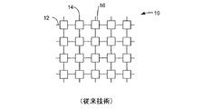
抵抗性ランダムアクセスメモリ(RAM)は、セルの上下の直交する方向に走る導体からなる2つのメッシュ間に挟まれる、離隔して配置されるメモリセルの平坦な行列からなる交点タイプのメモリアレイである。一例は、図1に示される抵抗性RAMアレイ10である。第1の方向に走る行導体12はワード線と呼ばれ、一般に第1の方向に垂直な第2の方向に延在する列導体14はビット線と呼ばれる。メモリセル16は通常、ワード線12と交差するビット線14とに接続されるように、正方形あるいは長方形のアレイに配列される。
【0003】
抵抗性RAMアレイでは、各メモリセルの各抵抗は2つ以上の状態を有し、メモリセル内のデータはセルの抵抗状態の関数である。抵抗性メモリセルは1つあるいは複数の磁性層、ヒューズまたはアンチヒューズ、あるいは素子の公称抵抗の大きさに影響を及ぼすことにより情報を格納または生成する任意の素子を含む場合がある。抵抗性RAMアレイにおいて用いられる他のタイプの抵抗性素子には、リードオンリーメモリの一部としてのポリシリコン抵抗、あるいは書換え可能メモリ素子としての相変化材料が含まれる。
【0004】
1つのタイプの抵抗性ランダムアクセスメモリが磁気ランダムアクセスメモリ(MRAM)であり、各メモリセルが、絶縁層によって分離される複数の磁性層から形成される。1つの磁性層はピン止め層と呼ばれ、対象の範囲内の磁界がかけられても磁気の向きが回転しないように固定される。別の磁性層はセンス層と呼ばれ、磁気の向きが、ピン止め層の状態に一致する状態と、ピン止め層の状態と一致しない状態との間で変化することができる。絶縁性トンネル障壁層は、磁気ピン止め層と磁気センス層との間に挟まれる。この絶縁性トンネル障壁層によって、センス層とピン止め層との間に、量子力学的トンネル現象が生じるようになる。トンネル現象は電子スピン依存性であり、メモリセルの抵抗を生じ、センス層およびピン止め層の磁化の相対的な向きの関数である。センス層の2つの状態の場合の接合抵抗の変化は、メモリセルに格納されるデータを決定する。2001年1月2日にBrug等に付与された下記特許文献1には、そのような磁気メモリセルが開示されている。
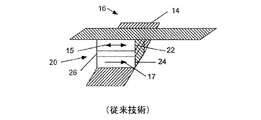
【0005】
図2を参照すると、MRAMメモリセルが示される。メモリユニット16は、3層メモリセル20として示される。各セル20では、セル20の磁気センス層22の向きにしたがって1ビットの情報が格納される。通常、セル20は論理状態「1」および「0」に対応する2つの安定した磁気状態を有する。センス層22上の双方向矢印15は、このバイナリ状態の能力を示す。セル20内のピン止め層24は、薄い絶縁体26によってセンス層から分離される。ピン止め層24は、層24上の一方向の矢印17によって示されるように、固定された磁気の向きを有する。センス層22の磁気状態がピン止め層24の磁化の向きと同じ方向に向けられるとき、セルの磁化は「平行」と呼ばれる。同様に、センス層22の磁気状態がピン止め層24の磁化の向きと反対の方向に向けられるとき、そのセルの磁化は「反平行」と呼ばれる。これらの向きは、それぞれ低抵抗状態と高抵抗状態とに対応する。
【0006】
選択されたメモリセル20の磁気状態は、選択されたメモリセルを横切るワード線12およびビット線14に電流を流すことにより変更されることができる。その電流は、2つの直交する磁界を生成し、それらが組み合わされるとき、選択されたメモリセル20の磁気の向きが平行状態と反平行状態との間で切り替えられることになる。他の選択されないメモリセルは、選択されないメモリセルを横切るワード線あるいはビット線のいずれか一方からの磁界のみを受ける。一つのの磁界は選択されないセルの磁気の向きを変更するほど強くはないので、それらのセルはその磁気の向きを保持する。
【0007】
図3を参照すると、MRAMメモリアレイ30が示される。センス増幅器32が選択されたメモリセル36のビット線34に接続される。電圧Vrが選択されたメモリセル36のワード線38に印加され、センス増幅器32は、セル36のビット線34に電圧を印加する。センス増幅器32は、メモリセル36の状態を反映する増幅された出力39を与える。同じビット線電圧が、全てのビット線34に印加され、選択されない行上の全てのセルを実効的にゼロ電位にバイアスする。この動作は互いからビット線電流を分離し、漏れ電流の大部分を実効的に遮断する。そうでなければ、二次的な経路を通って漏れ電流が流れることになり、選択されたメモリセルの読取り機能に誤りを生じる恐れがある。
【0008】
全てのメモリアレイに関連するいくつかの課題には、構造を簡略化することが必要なこと、メモリ記憶密度を向上させることが望ましいこと、アレイ内の導線を削減することが必要なことである。MRAMメモリアレイは、現時点で知られている最も簡単な記憶セルのうちの1つであるという点で第1の課題に非常に良好に対処する。メモリ記憶密度を向上させるための能力は通常、アレイ内の各セルのサイズを縮小することにより達成されている。導線の削減は、行および列に配列されるセルの数によって制限されている。
【0009】
【特許文献1】
米国特許第6,169,686号
【0010】
【発明が解決しようとする課題】
したがって、本発明の目的は、何よりも先にセルの寸法を縮小することなく、アレイ密度を向上させるための解決手法を提供することである。さらに本発明の別の目的は、2つのセル対で共通の経路を共有することにより、導体経路を削減するための解決手法を提供することである。
【0011】
【課題を解決するための手段】
本発明によれば、複数のメモリアレイプレーンを有するデータ記憶装置が開示される。データ記憶装置は、複数の磁気抵抗交点メモリセルの第1のアレイプレーンと、前記第1のアレイプレーンに平行な、複数の磁気抵抗性交点メモリセルの第2のアレイプレーンと、メモリセルの前記第1のアレイプレーンと前記第2のアレイプレーンとの間で共有される複数の導電性のワード線と、それぞれ前記第1のアレイプレーン内の1つのメモリセルを当該第1のアレイプレーン内の別の少なくとも1つのメモリセルに接続する、複数の第1のビット線と、それぞれ前記第2のアレイプレーン内の1つのメモリセルを当該第2のアレイプレーン内の別の少なくとも1つのメモリセルに接続する、複数の第2のビット線と、前記ワード線にアノード側が接続されるように、選択された前記ワード線に前記第1のアレイプレーンのうちの1つのメモリセルを接続する第1のダイオードと、前記ワード線にアノード側が接続されるように、選択された前記ワード線に前記第2のアレイプレーンのうちの1つのメモリセルを接続する第2のダイオードとを含む複数のダイオードと、を有している。前記ワード線を挟んで、前記第1のダイオードの順方向は、前記第2のダイオードの順方向に対して逆である。本発明は、前記第1のアレイプレーン内のメモリセルから、同じワード線を共有する前記第2のアレイプレーン内のメモリセルまで、前記第1のダイオードと前記第2のダイオードとを介して接続されている。
【0012】
データ記憶装置はさらに、それぞれ各ビット線によってメモリセルの1つあるいは複数のグループに接続され、関連するグループのメモリセル内を流れる電流を読み取るように動作することができる多数の読出し回路を含む。読出し回路はさらにセンス増幅器を含み、センス増幅器には電流モードセンス増幅器が用いられる場合がある。
【0013】
別の実施形態では、複数の磁気抵抗交点メモリセルの第1のアレイプレーンと、前記第1のアレイプレーンに平行な、複数の磁気抵抗性交点メモリセルの第2のアレイプレーンと、メモリセルの前記第1のアレイプレーンと前記第2のアレイプレーンとの間で共有される複数の導電性ワード線と、それぞれ前記第1のアレイプレーン内の1つのメモリセルを当該第1のアレイプレーン内の別の少なくとも1つのメモリセルに接続する、複数の第1のビット線と、それぞれ前記第2のアレイプレーン内の1つのメモリセルを当該第2のアレイプレーン内の別の少なくとも1つのメモリセルに接続する、複数の第2のビット線と、前記ワード線にアノード側が接続されるように、選択された前記ワード線に前記第1のアレイプレーンのうちの1つのメモリセルを接続する第1のダイオードと、前記ワード線にアノード側が接続されるように、選択された前記ワード線に前記第2のアレイプレーンのうちの1つのメモリセルを接続する第2のダイオードとを含む複数のダイオードを有し、前記ワード線を挟んで、前記第1のダイオードの順方向が、前記第2のダイオードの順方向に対して逆である、データ記憶装置におけるデータ読出し方法が開示される。データ読出し方法は、前記第1のアレイプレーンのアレイにバイアスを印加し、前記第1のアレイプレーンのうちの第1メモリセルと前記第2のアレイプレーンのうちの第2メモリセルにより共有されているワード線から、前記第1メモリセルを通して、対応する前記第1のビット線まで電流を流すステップと、前記第1のアレイプレーンのアレイにバイアスを印加している間、第2のアレイプレーンのアレイから前記第2メモリセルを通って電流が流れるのを阻止するステップと、を有する。第1および第2のダイオードについては、ダイオードが1つのメモリセルの干渉を防ぐいずれかのプレーン内の1つのメモリセルを、同じビット線を共有する別のメモリセルと接触するための役割を果す。
【0014】
本発明の他の態様および利点は、一例を用いて本発明の原理を説明する添付の図面とともに、以下に記載される詳細な説明から明らかになるであろう。
【0015】
【発明の実施の形態】
図4は、背合わせダイオードメモリセル構成を有する、共通ワード線プレーンを含むMRAMメモリセルアレイ100を示す。立体斜視図は、従来技術において通常必要とされる導線の数を削減しながらセル密度を向上させるために、多数のメモリセルが如何に配列されるかを示す。メモリアレイ100は、それぞれメモリセル108aおよび108bに対する共通導体としての役割を果たす、複数の行導線102a〜mを含む。単方向性導体110aおよび110bは、それぞれメモリセル108aおよび108bと係合する。単方向性スイッチ110aおよび110bによって、共通導体は、以下に記載される読出し、読取りおよび書込みプロセスにしたがって、他のセルがそのプロセスと干渉することなく、ビット対の一方のビットのみが読み出されるか、読み取られるか、あるいは書き込まれるように動作できるようになる。
【0016】
メモリアレイ100はさらに、第1の列導線104と第2の列導線106とを含む。複数の第1の列導線104a〜nが設けられ、同様に複数の第2の列導線106a〜nが設けられる。第1の列導線104aは、同じ列内に見られる各メモリセル108aの反対側に接続される。同様に、各第2の列導線106aはさらに、同じ列を共有する各メモリセル108bを接続する。単方向性導体110によって、読取り経路、書込み経路および読出し経路が共通行導体102で共有され、一対のメモリセル108aおよび108bが同じ行導体を共有できるようになる。
【0017】
行導体102はワード線として機能し、メモリセルアレイ100の一方にあるプレーン内でX方向に沿って延在する。第1の列導線104および第2の列導線106は、メモリセルアレイ100の別の側にあるプレーン内をY方向に沿って延在するビット線として機能する。この特定の実施形態では、アレイ100の2つの行に対して1つのワード線102が存在し、アレイ100の各列に対して2つのビット線104および106が存在する。各メモリセル108は、対応するワード線102とビット線104あるいは106のいずれかとの第1あるいは第2の交点に配置される。メモリセルアレイは、数千ではないにしても数百個のメモリセルを含むことができ、そして各行内のメモリセルの数と各列内のセルの数とは必ずしも等しい必要はないことに留意されたい。具体的には、行当たり少なくとも2つのメモリセルが存在するが、行当たりの列の対の数は一対一に対応する必要がないことが示されている。
【0018】
メモリセル108は、いずれか特定のタイプの素子には限定されない。上記のような、スピン依存トンネル素子が用いられる場合がある。「1」あるいは「0」を表すために各セルの磁化の向が決められ、メモリセル108にデータが格納される。たとえば、図4を参照すると、「0」の論理値は、センス層の磁化をピン止め層の磁気の向きに平行にしてメモリセル108に格納され、「1」の論理値は、センス層の磁化をピン止め層の磁気の向きに反対方向、すなわち反平行にしてメモリセルに格納される場合がある。さらに、相変化メモリセルとして知られる、相変化材料を利用して製造されるメモリセルが用いられる場合もある。
【0019】
図5は、本発明によるメモリアレイ100の概略的な立体斜視図を示す。メモリアレイ100は、メモリプレーン117a〜zからなる積重層を追加することが可能であることを示す。この例では、メモリプレーン117は垂直方向に積重可能なだけでなく、前後にも積重可能であり、結果として、マルチプレーンメモリアレイ内において導体プレーンメモリ素子が共有された立体格子が形成される。行導線102は、反対向きの単方向性導体110間に挿入され、一連の導体プレーン113が形成される。さらに、第1の列導体104がメモリ素子108の上側部分と係合し、一方、第2の列導体106がメモリ素子108の下側部分を接続する。列導体104および106は導体プレーン115a〜115yを形成する。単方向性素子110は通常、ダイオードのような一方向に電流を流す素子から構成される。
【0020】
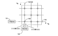
図6は、ワード線102およびビット線104を含む単一プレーン磁気ランダムアクセスメモリ(MRAM)素子610を示す。磁気トンネル接合108が、単一アレイプレーン100内のワード線102とビット線104との交点に配置される。このアレイは、列導体104の代わりに導体106を用いて示すこともでき、その場合には異なるプレーンが表されることになる。磁気トンネル接合108は行および列に配列され、その行はX方向に沿って延在し、その列はY方向に沿って延在する。アレイプレーン100内には、MRAM素子610の図を簡略化するために、比較的少数の磁気トンネル接合108のみが示される。実際には、任意のサイズのアレイを用いてもよい。
【0021】
ワード線102として機能するトレースは、アレイ100の一方にあるプレーン内をX方向に沿って延在する。ワード線102はダイオード110のアノードと接触している。ビット線104として機能するトレースは、アレイ100の隣接する側にあるプレーン内をY方向に沿って延在する。ビット線104は、磁気トンネル接合108のデータ層に接続される。
【0022】
またMRAM素子610は、第1および第2の行復号器120aおよび120b、第1および第2の列復号器122aおよび122b、及び読出し/書込み回路124を含む。読出し/書込み回路124は、センス増幅器、グランド接続子、行電流源、電圧源、及び列電流源を含む。
【0023】
選択された磁気トンネル接合108上での書込み動作中に、第1の行復号器120aは選択されたワード線102の一端を行電流源126に接続し、第2の行復号器120bは選択されたワード線120の反対側の端部をグランドに接続し、第1の列復号器122aは選択されたビット線104/106の一端をグランドに接続し、第2の列復号器122bは選択されたビット線104/106の反対側の端部を列電流源128に接続する。結果として、選択されたワード線102およびビット線104/106を通して書込み電流が流れる。
【0024】
書込み電流は、選択されたビットセルにおいて、選択された磁気トンネル接合108が切り替わるのに十分な合成磁界を生成する。ワード線102およびビット線104/106に沿った他の選択されないメモリセル108は、ワード線102あるいはビット線104/106のいずれかを流れる電流からの磁界のみを受ける。したがって、その磁界は十分な大きさではないので、選択されないメモリセルの状態は変更されないままである。
【0025】
選択された磁気トンネル接合108上での読出し動作中に、第1の行復号器120aは電圧源130を選択されたワード線102に接続し、第1の列復号器122bは選択されたビット線104/106を、センス増幅器118の仮想グランド入力に接続する。
【0026】
結果として、センス電流(IS)が選択された磁気トンネル接合108を通ってセンス増幅器118へ流れる。センス電流(IS)はセンス増幅器によって測定され、それゆえ、磁気トンネル接合108の抵抗および論理状態を決定することができる。
【0027】
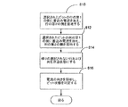
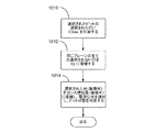
図7は、本発明によるメモリアレイ100上の書込み機能の概略図を示す。選択されたプレーンのメモリのアレイ内に1ビットのデータを書き込む方法は、図8の流れ図に略述されるようなステップを含む。最初に、ステップ810に示されるように、回路がそのビットの一方に書込み電流を加え、選択された1つあるいは複数のビットに対応する選択された行の他の側を接地する。次に、ステップ812に示されるように、回路が一方に書込み電流を加え、選択されたビットまたは複数ビットに対応する選択された列の他の側を接地する。その後、ステップ814によって示されるように、アレイは、全ての残りの選択されない行および列を浮動状態にすることができる。ステップ816では、メモリアレイは選択された列上の電流の方向を解析し、「1」が書き込まれたか、「0」が書き込まれたかを判定する。
【0028】
多数のビットを一度に書き込むことができるが、図6に示されるように、同時に書き込まれるビットは全て同じ行に接続されなければならない。さらに、行および列は、本発明による書込み機能の動作に関して交換可能として用いられる場合がある。
【0029】
導体プレーンの場合の読出し機能が、図9の概略図に示される。さらに、その方法が付随の図10に提示される。こうして、選択されたプレーンメモリのアレイ内の1ビットを読み出すために、ステップ1010に示されるように、システムは、選択されたビットに対応する選択された行に電圧V_biasを印加する(閉じられるように)。次に、ステップ1012に示されるように、アレイは、同じメモリプレーンの全ての選択されない行を、グランド電位あるいは当業者によって通常選択されるある共通の電圧を表す電圧Vgに接続する。その後、ステップ1014に示されるように、アレイは、選択された列(複数可)をセンス増幅器(複数可)に接続し、電流信号を読み出し、ビットの状態を判定する。この方法では、一度にメモリプレーン内の1つの行だけが選択される。さらに、図6の1アレイ当たり、同じ行上の多数のビットが同時に読み出される場合がある。
【0030】
図11は、ひとたび製造された結果の構造の断面図を示す。図12は図11の概略的な等価回路を示す。ビット対1100のこの部分では、2つのビット108aと108bとの間に共通の行導体102が配置される。ワード線導体102の両側にシリコンダイオード1110を製造することにより、接合部が形成される。第1のメモリセル108aは、第1の磁気ピン止め層材料1112を含む。ピン止め層1112上には、誘電体層1114が形成され、磁気データ層1116がその上に形成されるときのためのトンネル接合障壁としての役割を果たす。メモリビット108bは同じ構造を含むが、ワード線導体102に対してメモリビット108aと鏡像をなす。メモリアレイを製造する際に用いられるステップは、MRAMメモリセル製造技術の熟練者に知られている半導体プロセスの周知のステップと一致し、互換性がある。データ層およびピン止め層内の矢印は、これらの層のための磁界の向きを示す。
【0031】
1つの特定の実施形態では、行導体102はプラチナから形成され、プラチナ導体の両側にはシリコン材料が配置され、背合わせのショットキー障壁ダイオードあるいは単方向性導体110が形成される。その後、シリコン層に隣接してトンネル接合が形成され、結果として、ダイオード/MTJメモリセル110が形成される。この構造では、導体の3つの層が2つのメモリ層を構成し、そのプロセスは図6に示されるような多層メモリ素子を形成するために繰り返されることができる。
【0032】
本発明は従来技術より優れたいくつかの利点を有する。1つの利点は、必要とされる行導体プレーンが少なくてすみ、それにより1メモリプレーン当たり1つの行導体を有する従来技術において通常必要とされる余分な処理ステップが排除されることである。従来技術より優れた本発明の別の利点は、メモリプレーン内を多重化するために必要とされるトランジスタスイッチの数を削減することにより、経費が低減されることである。さらに別の利点は、最終的なメモリチップの素子サイズ全体が低減されることである。効率が高くなること、処理ステップのコストを削減できること、および密度を高くできることの全てが、従来技術より優れた本発明の大きな利点である。
【0033】
論理値は上記のように選択されたメモリセルに格納される。電圧が選択されたセルのワード線およびビット線に印加される場合、メモリセルの接合部内を流れる電流が、そのセルの磁化が平行であるか、反平行であるかを判定する。反平行の向きによって、MTJ抵抗が大きくなり、それにより選択されたメモリセルの接合内を流れる電流が小さくなることが好ましい。各メモリセルは、電源がない場合でも磁気の向きを保持することが好ましく、それゆえに「不揮発性」と呼ばれる。
【0034】
行および列導体は、銅、アルミニウムあるいは他の導電性材料のような高導電性の材料から形成されることが好ましい。MRAMメモリセルでは、ピン止め層は反強磁性材料から構成され、センス層は、ニッケル鉄、コバルト鉄あるいはニッケル鉄コバルトのような、磁界によって影響が及ぼされる強磁性材料から構成される。絶縁層は、Al2O3のような任意のタイプの絶縁材料から構成される場合があり、非常に薄く、通常は1〜5ナノメートル未満であり、トンネル電流が生じるようにする。
【0035】
上記の実施形態は本発明の代表的なものであるが、本明細書および添付の請求の範囲を検討することから、あるいは開示される本発明の実施形態を実施することから、他の実施形態が当業者には明らかになるであろう。本明細書およびそこに記載される実施形態は単なる例示とみなされ、本発明は請求の範囲およびその等価物によって規定されることが意図されている。
以下においては、本発明の種々の構成要件の組み合わせからなる例示的な実施態様を示す。
1. 平行なメモリプレーンを有するデータ記憶素子であって、
抵抗性交点メモリセルの第1のアレイプレーンと、
抵抗性交点メモリセルの第2のアレイプレーンと、
メモリセルの前記第1のプレーンと前記第2のプレーンとの間で共有される複数の導電性ワード線と、
それぞれ前記第1のプレーンからの1つのメモリセルを前記第2のプレーン内の別のメモリセルに接続する、複数のビット線と、
第1の導電方向において前記第1のプレーンからの1つのメモリセルを選択されたワード線と選択されたビット線とに接続する単方向性素子、及び第2の導電方向において前記第2のプレーンからの別のメモリセルを前記選択されたワード線と前記選択されたビット線とに接続する別の単方向性素子を含む複数の単方向性素子からなるデータ記憶素子。
2. 単方向性の導電性経路が、前記第1のプレーン内のメモリセルから、同じワード線を共有する前記第2のプレーン内のメモリセルまで形成される、上項1に記載のデータ記憶素子。
3. それぞれ個々のビット線によってメモリセルの1つあるいは複数のグループに接続され、関連するグループのメモリセル内を流れる電流を読み取るように動作することができる多数の読出し回路をさらに含む、上項1に記載のデータ記憶素子。
4. 前記読出し回路はそれぞれセンス増幅器を含む、上項3に記載のデータ記憶素子。
5. ワード線の選択されたグループ内の未選択ワード線は、前記センス増幅器の入力に印加される電圧に概ね等しい電圧に接続される、上項4に記載のデータ記憶素子。
6. 前記未選択ワード線は、前記選択されたビット線と同電位にバイアスをかけられる上項5に記載のデータ記憶素子。
7. 前記ワード線に接続され、前記抵抗性交点メモリセルアレイ内の電圧レベルを設定するように動作することができる等電位発生器を含み、選択された寄生電流が、読出しが行われていない隣接するメモリセルからのセンス電流と干渉するのを概ね防ぐか、あるいは前記選択された寄生電流の方向を逸らす上項1に記載のデータ記憶素子。
8. 前記等電位発生器は、メモリセルの各グループの共通の単方向性素子の入力ノードを設定し、共通のアレイ電圧を表す未選択ワード線からのフィードバックを阻止するように動作することができる、上項7に記載のデータ記憶素子。
9. データ記憶素子を形成するプロセスであって、
複数のワード線を形成し、
複数のビット線を形成し、
抵抗性交点メモリセルの第1のアレイプレーンを形成し、前記メモリセルをそれぞれ個々のビット線と個々のワード線とに接続し、抵抗性交点メモリセルの第2のアレイプレーンを形成し、前記第1のアレイプレーンからの1つのセルと前記第2のアレイプレーンからの1つのセルに共通のビット線およびワード線を共有させ、
前記アレイにバイアスをかけ、前記共通のワード線から、前記第1のアレイからの前記セルを通って、前記共通のビット線まで電流を流し、
前記アレイにバイアスをかけている間に、前記電流が前記第2のアレイから前記セルを通って流れるのを阻止することを含むプロセス。
10. 前記読出しプロセス中に、前記メモリセルを通って前記ワード線から前記ビット線まで単方向性の導電性経路を形成することを含む、上項9に記載のプロセス。
【0036】
【発明の効果】
本発明によれば、セルの寸法を縮小することなく、アレイ密度を向上させるための解決手法を実現することができる。さらに、2つのセルの対で共通の経路を共有することにより、導体経路を削減することもできる。
【図面の簡単な説明】
【図1】本発明による従来技術の抵抗性交点メモリセルを示す概略図である。
【図2】MRAMメモリセルとそれに接続される導体の従来技術の構造を示す概略図である。
【図3】本発明による読取り素子を有する従来技術のメモリアレイ構造を示す概略図である。
【図4】本発明による背合わせダイオードメモリセル構成を有する、共通ワード線プレーンを含むMRAMメモリセルアレイを示す図である。
【図5】図4のアレイに基づくマルチプレーンMRAMメモリセルアレイを示す図である。
【図6】本発明において考慮されるような対応する読出し/書込み回路を有するMRAMメモリセルアレイの概略図である。
【図7】本発明による図4のメモリプレーン上で実行されるような書込みプロセスを示す図である。
【図8】図7の書込みプロセスの流れ図である。
【図9】本発明による図4のメモリプレーン上で実行されるような読出しプロセスを示す図である。
【図10】図9の読出しプロセスの流れ図である。
【図11】本発明にしたがって製造されるようなMRAMメモリセルの断面図である。
【図12】本発明による図11のMRAMメモリセルの断面図の電気的な等価回路図である。
【符号の説明】
10 データ記憶素子
100 メモリアレイ
102 ワード線
104 ビット線
108 メモリセル
110 単方向性素子
117a〜z メモリプレーン[0001]
BACKGROUND OF THE INVENTION
The present invention relates to the field of resistive memory cell arrays. More particularly, the present invention relates to a memory array having memory bit pairs sharing a common conductor to increase array density.
[0002]
[Prior art]
A resistive random access memory (RAM) is an intersection type memory array consisting of a flat matrix of spaced apart memory cells sandwiched between two meshes of conductors that run in orthogonal directions above and below the cell. is there. An example is the
[0003]
In a resistive RAM array, each resistance of each memory cell has more than one state, and the data in the memory cell is a function of the resistance state of the cell. Resistive memory cells may include one or more magnetic layers, fuses or antifuses, or any element that stores or generates information by affecting the magnitude of the nominal resistance of the element. Other types of resistive elements used in resistive RAM arrays include polysilicon resistors as part of read-only memory, or phase change materials as rewritable memory elements.
[0004]
One type of resistive random access memory is a magnetic random access memory (MRAM), where each memory cell is formed from a plurality of magnetic layers separated by insulating layers. One magnetic layer is called a pinned layer, and is fixed so that the direction of magnetism does not rotate even when a magnetic field within a target range is applied. Another magnetic layer is called the sense layer, and the magnetic orientation can change between a state that matches the state of the pinned layer and a state that does not match the state of the pinned layer. The insulating tunnel barrier layer is sandwiched between the magnetic pinning layer and the magnetic sense layer. This insulating tunnel barrier layer causes a quantum mechanical tunnel phenomenon between the sense layer and the pinned layer. The tunneling phenomenon is electron spin dependent and causes the resistance of the memory cell and is a function of the relative orientation of the sense layer and pinned layer magnetization. The change in junction resistance in the two states of the sense layer determines the data stored in the memory cell. Such a magnetic memory cell is disclosed in Japanese Patent Application Laid-Open No. 2004-228688, which was granted to Brug et al. On January 2, 2001.
[0005]
Referring to FIG. 2, an MRAM memory cell is shown.
[0006]
The magnetic state of the
[0007]
Referring to FIG. 3, an
[0008]
Some challenges associated with all memory arrays require that the structure be simplified, that it is desirable to increase memory storage density, and that the wires in the array be reduced. . The MRAM memory array addresses the first problem very well in that it is one of the simplest storage cells known at the present time. The ability to increase memory storage density is typically achieved by reducing the size of each cell in the array. Lead reduction is limited by the number of cells arranged in rows and columns.
[0009]
[Patent Document 1]
US Pat. No. 6,169,686
[0010]
[Problems to be solved by the invention]
Accordingly, it is an object of the present invention to provide a solution for improving array density without reducing cell dimensions before anything else. Yet another object of the present invention is to provide a solution for reducing conductor paths by sharing a common path between two cell pairs.
[0011]
[Means for Solving the Problems]
According to the present invention, plural memory array Data storage with plane apparatus Is disclosed. Data storage device has multiple magnetoresistive intersections The first of the memory cells array Plain, A plurality of magnetoresistive intersections parallel to the first array plane Second of the memory cell array Plane and memory cell Said First array plane And said Second array Plain and of Multiple conductivity shared between of Word line and each Said First array plane A plurality of first bit lines for connecting one memory cell in the first array plane to at least one other memory cell in the first array plane, and one memory cell in the second array plane, respectively. A plurality of second bit lines connected to at least one other memory cell in the second array plane and the first word line selected to be connected to the word line so that the anode side is connected to the first word line A first diode that connects one memory cell of the array plane, and one memory cell of the second array plane that is connected to the selected word line so that an anode side is connected to the word line And a plurality of diodes including a second diode connecting the two. The forward direction of the first diode is opposite to the forward direction of the second diode across the word line. The present invention in front First array The second word sharing the same word line from the memory cells in the plane array To memory cells in the plane, Connected via the first diode and the second diode .
[0012]
Data storage apparatus Further includes a number of read circuits, each connected to one or more groups of memory cells by each bit line, and operable to read the current flowing in the associated group of memory cells. The read circuit further includes a sense amplifier, which may be a current mode sense amplifier.
[0013]
In another embodiment, A first array plane of a plurality of magnetoresistive intersection memory cells; a second array plane of a plurality of magnetoresistive intersection memory cells parallel to the first array plane; and the first array plane of memory cells. And a plurality of conductive word lines shared between the second array plane and one memory cell in the first array plane, respectively, and another at least one memory in the first array plane. A plurality of first bit lines connected to the cells and a plurality of first bit lines each connecting one memory cell in the second array plane to at least one other memory cell in the second array plane; One memory cell of the first array plane is connected to the selected word line so that the anode side is connected to the two bit lines and the word line A plurality of first diodes, and a second diode for connecting one memory cell of the second array plane to the selected word line so that an anode side is connected to the word line. A data reading method in a data storage device is disclosed in which the forward direction of the first diode is opposite to the forward direction of the second diode across the word line. A data read method applies a bias to the array of the first array plane and is shared by the first memory cell of the first array plane and the second memory cell of the second array plane. Flowing a current from a word line through the first memory cell to the corresponding first bit line, and applying a bias to the array of the first array plane, Blocking current from flowing through the second memory cell from the array. For the first and second diodes, diodes Serves to contact one memory cell in any plane that prevents interference of one memory cell with another memory cell sharing the same bit line.
[0014]
Other aspects and advantages of the present invention will become apparent from the following detailed description, taken in conjunction with the accompanying drawings, illustrating by way of example the principles of the invention.
[0015]
DETAILED DESCRIPTION OF THE INVENTION
FIG. 4 shows an MRAM
[0016]
[0017]
The
[0018]
[0019]
FIG. 5 shows a schematic three-dimensional perspective view of the
[0020]
FIG. 6 shows a single plane magnetic random access memory (MRAM)
[0021]
Traces that function as
[0022]
The
[0023]
During a write operation on the selected
[0024]
The write current generates a combined magnetic field that is sufficient for the selected
[0025]
During a read operation on the selected
[0026]
As a result, the sense current (I S ) Flows through the selected
[0027]
FIG. 7 shows a schematic diagram of the write function on the
[0028]
Multiple bits can be written at one time, but all bits written at the same time must be connected to the same row, as shown in FIG. Further, the rows and columns may be used interchangeably with respect to the operation of the write function according to the present invention.
[0029]
The readout function in the case of a conductor plane is shown in the schematic diagram of FIG. Further, the method is presented in accompanying FIG. Thus, to read one bit in the array of selected plane memories, the system applies (as closed) the voltage V_bias to the selected row corresponding to the selected bit, as shown in
[0030]
FIG. 11 shows a cross-sectional view of the resulting structure once manufactured. FIG. 12 shows a schematic equivalent circuit of FIG. In this portion of
[0031]
In one particular embodiment, the
[0032]
The present invention has several advantages over the prior art. One advantage is that fewer row conductor planes are required, thereby eliminating the extra processing steps normally required in the prior art with one row conductor per memory plane. Another advantage of the present invention over the prior art is that it reduces costs by reducing the number of transistor switches required to multiplex within the memory plane. Yet another advantage is that the overall device size of the final memory chip is reduced. Increased efficiency, reduced processing step costs, and increased density are all significant advantages of the present invention over the prior art.
[0033]
The logical value is stored in the memory cell selected as described above. When a voltage is applied to the word line and bit line of the selected cell, the current flowing through the junction of the memory cell determines whether the magnetization of that cell is parallel or anti-parallel. Preferably, the antiparallel orientation increases the MTJ resistance, thereby reducing the current flowing through the junction of the selected memory cell. Each memory cell preferably retains its magnetic orientation even when there is no power supply and is therefore referred to as “non-volatile”.
[0034]
The row and column conductors are preferably formed from a highly conductive material such as copper, aluminum or other conductive material. In an MRAM memory cell, the pinned layer is made of an antiferromagnetic material, and the sense layer is made of a ferromagnetic material that is affected by a magnetic field, such as nickel iron, cobalt iron, or nickel iron cobalt. Insulating layer is made of Al 2 O 3 May be composed of any type of insulating material, such as:
[0035]
While the above embodiments are representative of the present invention, other embodiments may be considered from a consideration of the specification and the appended claims, or from implementing the disclosed embodiments of the invention. Will be apparent to those skilled in the art. It is intended that the specification and embodiments described herein be considered as exemplary only and that the invention be defined by the claims and their equivalents.
In the following, exemplary embodiments consisting of combinations of various constituents of the present invention are shown.
1. A data storage element having parallel memory planes,
A first array plane of resistive intersection memory cells;
A second array plane of resistive intersection memory cells;
A plurality of conductive word lines shared between the first plane and the second plane of memory cells;
A plurality of bit lines each connecting one memory cell from the first plane to another memory cell in the second plane;
A unidirectional element connecting one memory cell from the first plane in the first conductive direction to a selected word line and a selected bit line; and the second plane in a second conductive direction. A data storage element comprising a plurality of unidirectional elements including another unidirectional element connecting another memory cell from a selected word line and the selected bit line.
2. The data storage element according to claim 1, wherein a unidirectional conductive path is formed from a memory cell in the first plane to a memory cell in the second plane sharing the same word line.
3. The above paragraph 1 further includes a number of read circuits connected to one or more groups of memory cells, each by an individual bit line, and operable to read current flowing in the memory cells of the associated group. The data storage element described.
4). 4. The data storage element according to item 3, wherein each of the read circuits includes a sense amplifier.
5. The data storage element of claim 4, wherein unselected word lines in a selected group of word lines are connected to a voltage generally equal to a voltage applied to an input of the sense amplifier.
6). 6. The data storage element according to claim 5, wherein the unselected word line is biased to the same potential as the selected bit line.
7). An adjacent memory connected to the word line and including an equipotential generator operable to set a voltage level in the resistive intersection memory cell array, wherein the selected parasitic current is not read The data storage element of claim 1, wherein the data storage element generally prevents interference with a sense current from the cell or diverts the direction of the selected parasitic current.
8). The equipotential generator is operable to set an input node of a common unidirectional element for each group of memory cells and prevent feedback from unselected word lines representing a common array voltage. 8. The data storage element according to item 7.
9. A process for forming a data storage element comprising:
Forming multiple word lines,
Forming multiple bit lines,
Forming a first array plane of resistive intersection memory cells, connecting the memory cells to individual bit lines and individual word lines, respectively, forming a second array plane of resistive intersection memory cells; Sharing a common bit line and word line for one cell from the first array plane and one cell from the second array plane;
Bias the array to pass current from the common word line through the cells from the first array to the common bit line;
Preventing the current from flowing from the second array through the cell while biasing the array.
10. The process of claim 9, comprising forming a unidirectional conductive path through the memory cell from the word line to the bit line during the read process.
[0036]
【The invention's effect】
According to the present invention, it is possible to realize a solution for improving the array density without reducing the cell dimensions. Further, by sharing a common path between two cell pairs, the conductor path can be reduced.
[Brief description of the drawings]
FIG. 1 is a schematic diagram illustrating a prior art resistive intersection memory cell according to the present invention.
FIG. 2 is a schematic diagram showing a prior art structure of an MRAM memory cell and a conductor connected thereto.
FIG. 3 is a schematic diagram illustrating a prior art memory array structure having a read element according to the present invention.
FIG. 4 is a diagram illustrating an MRAM memory cell array including a common word line plane having a back-to-back diode memory cell configuration according to the present invention.
5 shows a multi-plane MRAM memory cell array based on the array of FIG.
FIG. 6 is a schematic diagram of an MRAM memory cell array with corresponding read / write circuits as contemplated in the present invention.
7 illustrates a write process as performed on the memory plane of FIG. 4 according to the present invention.
8 is a flowchart of the write process of FIG.
9 illustrates a read process as performed on the memory plane of FIG. 4 according to the present invention.
FIG. 10 is a flowchart of the read process of FIG.
FIG. 11 is a cross-sectional view of an MRAM memory cell as manufactured in accordance with the present invention.
12 is an electrical equivalent circuit diagram of a cross-sectional view of the MRAM memory cell of FIG. 11 in accordance with the present invention.
[Explanation of symbols]
10 Data storage elements
100 memory array
102 word lines
104 bit line
108 memory cells
110 Unidirectional element
117a-z Memory plane
Claims (16)
複数の磁気抵抗交点メモリセルの第1のアレイプレーンと、
前記第1のアレイプレーンに平行な、複数の磁気抵抗性交点メモリセルの第2のアレイプレーンと、
メモリセルの前記第1のアレイプレーンと前記第2のアレイプレーンとの間で共有される複数の導電性のワード線と、
それぞれ前記第1のアレイプレーン内の1つのメモリセルを当該第1のアレイプレーン内の別の少なくとも1つのメモリセルに接続する、複数の第1のビット線と、
それぞれ前記第2のアレイプレーン内の1つのメモリセルを当該第2のアレイプレーン内の別の少なくとも1つのメモリセルに接続する、複数の第2のビット線と、
前記ワード線にアノード側が接続されるように、選択された前記ワード線に前記第1のアレイプレーンのうちの1つのメモリセルを接続する第1のダイオードと、前記ワード線にアノード側が接続されるように、選択された前記ワード線に前記第2のアレイプレーンのうちの1つのメモリセルを接続する第2のダイオードとを含む複数のダイオードと、を有しており、
前記ワード線を挟んで、前記第1のダイオードの順方向は、前記第2のダイオードの順方向に対して逆であることを特徴とする、データ記憶装置。A data storage device having a plurality of memory array planes,
A first array plane of a plurality of magnetoresistive intersection memory cells;
A second array plane of a plurality of magnetoresistive intersection memory cells parallel to the first array plane;
A plurality of conductive word lines are shared between the first array plane of memory cells and the second array plane,
Each connecting one memory cell of said first array plane to another of the at least one memory cell of said first array plane, and a plurality of first bit lines,
A plurality of second bit lines each connecting one memory cell in the second array plane to at least one other memory cell in the second array plane;
A first diode that connects one memory cell of the first array plane to the selected word line and an anode side to the word line so that the anode side is connected to the word line. And a plurality of diodes including a second diode that connects one memory cell of the second array plane to the selected word line,
A data storage device , wherein the forward direction of the first diode is opposite to the forward direction of the second diode across the word line .
前記第1のアレイプレーンに平行な、複数の磁気抵抗性交点メモリセルの第2のアレイプレーンと、
メモリセルの前記第1のアレイプレーンと前記第2のアレイプレーンとの間で共有される複数の導電性ワード線と、
それぞれ前記第1のアレイプレーン内の1つのメモリセルを当該第1のアレイプレーン内の別の少なくとも1つのメモリセルに接続する、複数の第1のビット線と、
それぞれ前記第2のアレイプレーン内の1つのメモリセルを当該第2のアレイプレーン内の別の少なくとも1つのメモリセルに接続する、複数の第2のビット線と、
前記ワード線にアノード側が接続されるように、選択された前記ワード線に前記第1のアレイプレーンのうちの1つのメモリセルを接続する第1のダイオードと、前記ワード線にアノード側が接続されるように、選択された前記ワード線に前記第2のアレイプレーンのうちの1つのメモリセルを接続する第2のダイオードとを含む複数のダイオードを有し、
前記ワード線を挟んで、前記第1のダイオードの順方向が、前記第2のダイオードの順方向に対して逆である、データ記憶装置におけるデータ読出し方法であって、
前記第1のアレイプレーンのアレイにバイアスを印加し、前記第1のアレイプレーンのうちの第1メモリセルと前記第2のアレイプレーンのうちの第2メモリセルにより共有されているワード線から、前記第1メモリセルを通して、対応する前記第1のビット線まで電流を流すステップと、
前記第1のアレイプレーンのアレイにバイアスを印加している間、第2のアレイプレーンのアレイから前記第2メモリセルを通って電流が流れるのを阻止するステップと、を有することを特徴とするデータの読出し方法。 A first array plane of a plurality of magnetoresistive intersection memory cells;
A second array plane of a plurality of magnetoresistive intersection memory cells parallel to the first array plane;
A plurality of conductive word lines shared between the first array plane and the second array plane of memory cells;
A plurality of first bit lines each connecting one memory cell in the first array plane to at least one other memory cell in the first array plane;
A plurality of second bit lines each connecting one memory cell in the second array plane to at least one other memory cell in the second array plane;
A first diode that connects one memory cell of the first array plane to the selected word line and an anode side to the word line so that the anode side is connected to the word line. And a plurality of diodes including a second diode connecting one memory cell of the second array plane to the selected word line,
A data reading method in a data storage device, wherein the forward direction of the first diode is opposite to the forward direction of the second diode across the word line ,
Applying a bias to the array of first array planes, from a word line shared by a first memory cell of the first array plane and a second memory cell of the second array plane ; Passing a current through the first memory cell to the corresponding first bit line;
And having between the steps to prevent current from flowing through said second memory cell from the second array of array plane, the the application of the bias to the first array of the array plane How to read data .
Applications Claiming Priority (2)
| Application Number | Priority Date | Filing Date | Title |
|---|---|---|---|
| US10/098903 | 2002-03-14 | ||
| US10/098,903 US6778421B2 (en) | 2002-03-14 | 2002-03-14 | Memory device array having a pair of magnetic bits sharing a common conductor line |
Publications (3)
| Publication Number | Publication Date |
|---|---|
| JP2004031914A JP2004031914A (en) | 2004-01-29 |
| JP2004031914A5 JP2004031914A5 (en) | 2006-05-11 |
| JP4700259B2 true JP4700259B2 (en) | 2011-06-15 |
Family
ID=27765436
Family Applications (1)
| Application Number | Title | Priority Date | Filing Date |
|---|---|---|---|
| JP2003069239A Expired - Fee Related JP4700259B2 (en) | 2002-03-14 | 2003-03-14 | Memory element array having a pair of magnetic bits sharing a common conductor |
Country Status (6)
| Country | Link |
|---|---|
| US (2) | US6778421B2 (en) |
| EP (1) | EP1345232A3 (en) |
| JP (1) | JP4700259B2 (en) |
| KR (1) | KR101010321B1 (en) |
| CN (1) | CN100481551C (en) |
| TW (1) | TW200304142A (en) |
Families Citing this family (105)
| Publication number | Priority date | Publication date | Assignee | Title |
|---|---|---|---|---|
| US6940748B2 (en) * | 2002-05-16 | 2005-09-06 | Micron Technology, Inc. | Stacked 1T-nMTJ MRAM structure |
| WO2003098636A2 (en) * | 2002-05-16 | 2003-11-27 | Micron Technology, Inc. | STACKED 1T-nMEMORY CELL STRUCTURE |
| US6801450B2 (en) * | 2002-05-22 | 2004-10-05 | Hewlett-Packard Development Company, L.P. | Memory cell isolation |
| US6917532B2 (en) * | 2002-06-21 | 2005-07-12 | Hewlett-Packard Development Company, L.P. | Memory storage device with segmented column line array |
| US7081377B2 (en) * | 2002-06-27 | 2006-07-25 | Sandisk 3D Llc | Three-dimensional memory |
| US6882553B2 (en) * | 2002-08-08 | 2005-04-19 | Micron Technology Inc. | Stacked columnar resistive memory structure and its method of formation and operation |
| US6577529B1 (en) * | 2002-09-03 | 2003-06-10 | Hewlett-Packard Development Company, L.P. | Multi-bit magnetic memory device |
| US6778420B2 (en) * | 2002-09-25 | 2004-08-17 | Ovonyx, Inc. | Method of operating programmable resistant element |
| US7618850B2 (en) * | 2002-12-19 | 2009-11-17 | Sandisk 3D Llc | Method of making a diode read/write memory cell in a programmed state |
| US20070164388A1 (en) * | 2002-12-19 | 2007-07-19 | Sandisk 3D Llc | Memory cell comprising a diode fabricated in a low resistivity, programmed state |
| US7660181B2 (en) * | 2002-12-19 | 2010-02-09 | Sandisk 3D Llc | Method of making non-volatile memory cell with embedded antifuse |
| US8008700B2 (en) * | 2002-12-19 | 2011-08-30 | Sandisk 3D Llc | Non-volatile memory cell with embedded antifuse |
| US7800933B2 (en) * | 2005-09-28 | 2010-09-21 | Sandisk 3D Llc | Method for using a memory cell comprising switchable semiconductor memory element with trimmable resistance |
| US7800932B2 (en) | 2005-09-28 | 2010-09-21 | Sandisk 3D Llc | Memory cell comprising switchable semiconductor memory element with trimmable resistance |
| US7505321B2 (en) * | 2002-12-31 | 2009-03-17 | Sandisk 3D Llc | Programmable memory array structure incorporating series-connected transistor strings and methods for fabrication and operation of same |
| WO2004084228A1 (en) | 2003-03-18 | 2004-09-30 | Kabushiki Kaisha Toshiba | Phase change memory device |
| US20050006719A1 (en) * | 2003-06-24 | 2005-01-13 | Erh-Kun Lai | [three-dimensional memory structure and manufacturing method thereof] |
| JP4534441B2 (en) * | 2003-07-25 | 2010-09-01 | Tdk株式会社 | Magnetic memory cell and magnetic memory device using the same |
| EP1626411A1 (en) * | 2004-08-13 | 2006-02-15 | STMicroelectronics S.r.l. | Shared address lines for crosspoint memory |
| KR100657944B1 (en) | 2005-01-12 | 2006-12-14 | 삼성전자주식회사 | Method of operating Phase change Random Access MemoryPRAM |
| KR100688540B1 (en) * | 2005-03-24 | 2007-03-02 | 삼성전자주식회사 | Semiconductor memory device with improved memory cell density |
| KR100604935B1 (en) * | 2005-03-24 | 2006-07-28 | 삼성전자주식회사 | Semiconductor memory device with reduced core size |
| US9390790B2 (en) * | 2005-04-05 | 2016-07-12 | Nantero Inc. | Carbon based nonvolatile cross point memory incorporating carbon based diode select devices and MOSFET select devices for memory and logic applications |
| KR100699848B1 (en) * | 2005-06-21 | 2007-03-27 | 삼성전자주식회사 | Phase change random access memory having improved core structure |
| KR100688553B1 (en) * | 2005-06-22 | 2007-03-02 | 삼성전자주식회사 | Phase Change Random Access Memory device having reduced core layout size |
| CN100424554C (en) * | 2005-09-07 | 2008-10-08 | 爱普生映像元器件有限公司 | Electro-optical device and electronic apparatus |
| US7283389B2 (en) * | 2005-12-09 | 2007-10-16 | Macronix International Co., Ltd. | Gated diode nonvolatile memory cell array |
| US20070132049A1 (en) * | 2005-12-12 | 2007-06-14 | Stipe Barry C | Unipolar resistance random access memory (RRAM) device and vertically stacked architecture |
| KR100695171B1 (en) * | 2006-02-23 | 2007-03-14 | 삼성전자주식회사 | Magnetic memory apparatus using magnetic domain motion |
| US8395199B2 (en) | 2006-03-25 | 2013-03-12 | 4D-S Pty Ltd. | Systems and methods for fabricating self-aligned memory cell |
| US8120949B2 (en) * | 2006-04-27 | 2012-02-21 | Avalanche Technology, Inc. | Low-cost non-volatile flash-RAM memory |
| US7932548B2 (en) | 2006-07-14 | 2011-04-26 | 4D-S Pty Ltd. | Systems and methods for fabricating self-aligned memory cell |
| US7486537B2 (en) * | 2006-07-31 | 2009-02-03 | Sandisk 3D Llc | Method for using a mixed-use memory array with different data states |
| US20080025069A1 (en) * | 2006-07-31 | 2008-01-31 | Scheuerlein Roy E | Mixed-use memory array with different data states |
| US7450414B2 (en) * | 2006-07-31 | 2008-11-11 | Sandisk 3D Llc | Method for using a mixed-use memory array |
| JP4577695B2 (en) * | 2006-11-07 | 2010-11-10 | エルピーダメモリ株式会社 | Semiconductor memory device and manufacturing method of semiconductor memory device |
| KR100837412B1 (en) * | 2006-12-12 | 2008-06-12 | 삼성전자주식회사 | Multi-stack memory device |
| KR100881292B1 (en) | 2007-01-23 | 2009-02-04 | 삼성전자주식회사 | Resistive semiconductor memory device having three dimension stack structure and method for controlling the same |
| US8987702B2 (en) | 2007-05-01 | 2015-03-24 | Micron Technology, Inc. | Selectively conducting devices, diode constructions, constructions, and diode forming methods |
| US8487450B2 (en) * | 2007-05-01 | 2013-07-16 | Micron Technology, Inc. | Semiconductor constructions comprising vertically-stacked memory units that include diodes utilizing at least two different dielectric materials, and electronic systems |
| JP5157268B2 (en) * | 2007-06-13 | 2013-03-06 | 株式会社日立製作所 | Spin accumulation magnetization reversal type memory device and spin RAM |
| US8102694B2 (en) * | 2007-06-25 | 2012-01-24 | Sandisk 3D Llc | Nonvolatile memory device containing carbon or nitrogen doped diode |
| US8072791B2 (en) * | 2007-06-25 | 2011-12-06 | Sandisk 3D Llc | Method of making nonvolatile memory device containing carbon or nitrogen doped diode |
| US7684226B2 (en) * | 2007-06-25 | 2010-03-23 | Sandisk 3D Llc | Method of making high forward current diodes for reverse write 3D cell |
| US7830697B2 (en) * | 2007-06-25 | 2010-11-09 | Sandisk 3D Llc | High forward current diodes for reverse write 3D cell |
| JP4468414B2 (en) * | 2007-06-29 | 2010-05-26 | 株式会社東芝 | Resistance change memory device |
| CN101878529B (en) * | 2007-11-29 | 2012-07-04 | 松下电器产业株式会社 | Nonvolatile storage device and method for manufacturing the same |
| US8198618B2 (en) * | 2007-12-10 | 2012-06-12 | Panasonic Corporation | Nonvolatile memory device and manufacturing method thereof |
| US7768812B2 (en) | 2008-01-15 | 2010-08-03 | Micron Technology, Inc. | Memory cells, memory cell programming methods, memory cell reading methods, memory cell operating methods, and memory devices |
| US8034655B2 (en) | 2008-04-08 | 2011-10-11 | Micron Technology, Inc. | Non-volatile resistive oxide memory cells, non-volatile resistive oxide memory arrays, and methods of forming non-volatile resistive oxide memory cells and memory arrays |
| US7830698B2 (en) * | 2008-04-11 | 2010-11-09 | Sandisk 3D Llc | Multilevel nonvolatile memory device containing a carbon storage material and methods of making and using same |
| US7812335B2 (en) * | 2008-04-11 | 2010-10-12 | Sandisk 3D Llc | Sidewall structured switchable resistor cell |
| US8659852B2 (en) * | 2008-04-21 | 2014-02-25 | Seagate Technology Llc | Write-once magentic junction memory array |
| US8211743B2 (en) | 2008-05-02 | 2012-07-03 | Micron Technology, Inc. | Methods of forming non-volatile memory cells having multi-resistive state material between conductive electrodes |
| US8134194B2 (en) * | 2008-05-22 | 2012-03-13 | Micron Technology, Inc. | Memory cells, memory cell constructions, and memory cell programming methods |
| US8120951B2 (en) | 2008-05-22 | 2012-02-21 | Micron Technology, Inc. | Memory devices, memory device constructions, constructions, memory device forming methods, current conducting devices, and memory cell programming methods |
| US7852663B2 (en) * | 2008-05-23 | 2010-12-14 | Seagate Technology Llc | Nonvolatile programmable logic gates and adders |
| US7855911B2 (en) * | 2008-05-23 | 2010-12-21 | Seagate Technology Llc | Reconfigurable magnetic logic device using spin torque |
| US8134137B2 (en) | 2008-06-18 | 2012-03-13 | Micron Technology, Inc. | Memory device constructions, memory cell forming methods, and semiconductor construction forming methods |
| US9343665B2 (en) | 2008-07-02 | 2016-05-17 | Micron Technology, Inc. | Methods of forming a non-volatile resistive oxide memory cell and methods of forming a non-volatile resistive oxide memory array |
| US8014185B2 (en) * | 2008-07-09 | 2011-09-06 | Sandisk 3D Llc | Multiple series passive element matrix cell for three-dimensional arrays |
| US7881098B2 (en) | 2008-08-26 | 2011-02-01 | Seagate Technology Llc | Memory with separate read and write paths |
| US7985994B2 (en) | 2008-09-29 | 2011-07-26 | Seagate Technology Llc | Flux-closed STRAM with electronically reflective insulative spacer |
| US8169810B2 (en) | 2008-10-08 | 2012-05-01 | Seagate Technology Llc | Magnetic memory with asymmetric energy barrier |
| US8039913B2 (en) * | 2008-10-09 | 2011-10-18 | Seagate Technology Llc | Magnetic stack with laminated layer |
| US8089132B2 (en) | 2008-10-09 | 2012-01-03 | Seagate Technology Llc | Magnetic memory with phonon glass electron crystal material |
| JP5127661B2 (en) * | 2008-10-10 | 2013-01-23 | 株式会社東芝 | Semiconductor memory device |
| US20100102405A1 (en) * | 2008-10-27 | 2010-04-29 | Seagate Technology Llc | St-ram employing a spin filter |
| US8045366B2 (en) | 2008-11-05 | 2011-10-25 | Seagate Technology Llc | STRAM with composite free magnetic element |
| KR101012435B1 (en) * | 2008-11-10 | 2011-02-08 | 주식회사 하이닉스반도체 | Phase change memory device and method for manufacturing the same |
| US8043732B2 (en) | 2008-11-11 | 2011-10-25 | Seagate Technology Llc | Memory cell with radial barrier |
| US7826181B2 (en) * | 2008-11-12 | 2010-11-02 | Seagate Technology Llc | Magnetic memory with porous non-conductive current confinement layer |
| US8289756B2 (en) | 2008-11-25 | 2012-10-16 | Seagate Technology Llc | Non volatile memory including stabilizing structures |
| US7826259B2 (en) * | 2009-01-29 | 2010-11-02 | Seagate Technology Llc | Staggered STRAM cell |
| US8304755B2 (en) * | 2009-02-18 | 2012-11-06 | Macronix International Co., Ltd. | Three-dimensional semiconductor structure |
| US8144506B2 (en) | 2009-06-23 | 2012-03-27 | Micron Technology, Inc. | Cross-point memory devices, electronic systems including cross-point memory devices and methods of accessing a plurality of memory cells in a cross-point memory array |
| US7999338B2 (en) | 2009-07-13 | 2011-08-16 | Seagate Technology Llc | Magnetic stack having reference layers with orthogonal magnetization orientation directions |
| US8411477B2 (en) | 2010-04-22 | 2013-04-02 | Micron Technology, Inc. | Arrays of vertically stacked tiers of non-volatile cross point memory cells, methods of forming arrays of vertically stacked tiers of non-volatile cross point memory cells, and methods of reading a data value stored by an array of vertically stacked tiers of non-volatile cross point memory cells |
| US8427859B2 (en) | 2010-04-22 | 2013-04-23 | Micron Technology, Inc. | Arrays of vertically stacked tiers of non-volatile cross point memory cells, methods of forming arrays of vertically stacked tiers of non-volatile cross point memory cells, and methods of reading a data value stored by an array of vertically stacked tiers of non-volatile cross point memory cells |
| US8289763B2 (en) | 2010-06-07 | 2012-10-16 | Micron Technology, Inc. | Memory arrays |
| CN101894771B (en) * | 2010-06-22 | 2012-02-22 | 中国科学院上海微系统与信息技术研究所 | Manufacturing method of multilayer stacked resistance transit storage |
| US8441836B2 (en) * | 2010-09-17 | 2013-05-14 | Ovonyx, Inc. | Sector array addressing for ECC management |
| US8351242B2 (en) | 2010-09-29 | 2013-01-08 | Micron Technology, Inc. | Electronic devices, memory devices and memory arrays |
| US8759809B2 (en) | 2010-10-21 | 2014-06-24 | Micron Technology, Inc. | Integrated circuitry comprising nonvolatile memory cells having platelike electrode and ion conductive material layer |
| US8796661B2 (en) | 2010-11-01 | 2014-08-05 | Micron Technology, Inc. | Nonvolatile memory cells and methods of forming nonvolatile memory cell |
| US8526213B2 (en) | 2010-11-01 | 2013-09-03 | Micron Technology, Inc. | Memory cells, methods of programming memory cells, and methods of forming memory cells |
| EP2641246B1 (en) * | 2010-11-19 | 2016-02-24 | Hewlett-Packard Development Company, L.P. | Circuit and method for reading a resistive switching device in an array |
| US9454997B2 (en) | 2010-12-02 | 2016-09-27 | Micron Technology, Inc. | Array of nonvolatile memory cells having at least five memory cells per unit cell, having a plurality of the unit cells which individually comprise three elevational regions of programmable material, and/or having a continuous volume having a combination of a plurality of vertically oriented memory cells and a plurality of horizontally oriented memory cells; array of vertically stacked tiers of nonvolatile memory cells |
| US8431458B2 (en) | 2010-12-27 | 2013-04-30 | Micron Technology, Inc. | Methods of forming a nonvolatile memory cell and methods of forming an array of nonvolatile memory cells |
| US8791447B2 (en) | 2011-01-20 | 2014-07-29 | Micron Technology, Inc. | Arrays of nonvolatile memory cells and methods of forming arrays of nonvolatile memory cells |
| US8488365B2 (en) | 2011-02-24 | 2013-07-16 | Micron Technology, Inc. | Memory cells |
| EP2686883B1 (en) | 2011-03-29 | 2015-07-01 | Hewlett-Packard Development Company, L.P. | Dual-plane memory array |
| US8537592B2 (en) | 2011-04-15 | 2013-09-17 | Micron Technology, Inc. | Arrays of nonvolatile memory cells and methods of forming arrays of nonvolatile memory cells |
| CN103514956B (en) * | 2012-06-15 | 2016-04-13 | 晶豪科技股份有限公司 | Semiconductor memery device and method of testing thereof |
| CN103794618A (en) * | 2012-11-02 | 2014-05-14 | 北京大学 | Bipolar resistive memory device |
| US10249684B2 (en) * | 2012-12-17 | 2019-04-02 | Nantero, Inc. | Resistive change elements incorporating carbon based diode select devices |
| US9349450B2 (en) * | 2013-06-10 | 2016-05-24 | Micron Technology, Inc. | Memory devices and memory operational methods including single erase operation of conductive bridge memory cells |
| WO2015065316A1 (en) * | 2013-10-28 | 2015-05-07 | Hewlett-Packard Development Company, L.P. | Geometry dependent voltage biases for asymmetric resistive memories |
| CN105514262A (en) * | 2015-10-30 | 2016-04-20 | 上海磁宇信息科技有限公司 | Crossing matrix array magnetic random memory manufacturing process |
| US9837602B2 (en) * | 2015-12-16 | 2017-12-05 | Western Digital Technologies, Inc. | Spin-orbit torque bit design for improved switching efficiency |
| US9614002B1 (en) * | 2016-01-21 | 2017-04-04 | Samsung Electronics Co., Ltd. | 0T bi-directional memory cell |
| US9858975B1 (en) * | 2016-08-24 | 2018-01-02 | Samsung Electronics Co., Ltd. | Zero transistor transverse current bi-directional bitcell |
| US9806256B1 (en) | 2016-10-21 | 2017-10-31 | Sandisk Technologies Llc | Resistive memory device having sidewall spacer electrode and method of making thereof |
| US10790002B2 (en) | 2018-06-21 | 2020-09-29 | Samsung Electronics Co., Ltd. | Giant spin hall-based compact neuromorphic cell optimized for differential read inference |
| US11437083B2 (en) | 2021-02-05 | 2022-09-06 | International Business Machines Corporation | Two-bit magnetoresistive random-access memory device architecture |
Citations (3)
| Publication number | Priority date | Publication date | Assignee | Title |
|---|---|---|---|---|
| WO2000057423A1 (en) * | 1999-03-19 | 2000-09-28 | Infineon Technologies Ag | Storage cell array and method for the production thereof |
| JP2001519582A (en) * | 1997-10-06 | 2001-10-23 | インフィネオン テクノロジース アクチエンゲゼルシャフト | Memory cell device |
| JP2002025245A (en) * | 2000-06-30 | 2002-01-25 | Nec Corp | Nonvolatile semiconductor storage device and information recording method |
Family Cites Families (22)
| Publication number | Priority date | Publication date | Assignee | Title |
|---|---|---|---|---|
| US4646266A (en) * | 1984-09-28 | 1987-02-24 | Energy Conversion Devices, Inc. | Programmable semiconductor structures and methods for using the same |
| US5497965A (en) * | 1994-05-27 | 1996-03-12 | Mathieu, Jr.; Edward F. | Releasable microphone stand apparatus |
| US5640343A (en) | 1996-03-18 | 1997-06-17 | International Business Machines Corporation | Magnetic memory array using magnetic tunnel junction devices in the memory cells |
| US6169686B1 (en) | 1997-11-20 | 2001-01-02 | Hewlett-Packard Company | Solid-state memory with magnetic storage cells |
| US5991193A (en) | 1997-12-02 | 1999-11-23 | International Business Machines Corporation | Voltage biasing for magnetic ram with magnetic tunnel memory cells |
| US6130835A (en) | 1997-12-02 | 2000-10-10 | International Business Machines Corporation | Voltage biasing for magnetic RAM with magnetic tunnel memory cells |
| US6081446A (en) | 1998-06-03 | 2000-06-27 | Hewlett-Packard Company | Multiple bit magnetic memory cell |
| US6034887A (en) * | 1998-08-05 | 2000-03-07 | International Business Machines Corporation | Non-volatile magnetic memory cell and devices |
| TW440835B (en) * | 1998-09-30 | 2001-06-16 | Siemens Ag | Magnetoresistive memory with raised interference security |
| US6034882A (en) * | 1998-11-16 | 2000-03-07 | Matrix Semiconductor, Inc. | Vertically stacked field programmable nonvolatile memory and method of fabrication |
| US6351406B1 (en) * | 1998-11-16 | 2002-02-26 | Matrix Semiconductor, Inc. | Vertically stacked field programmable nonvolatile memory and method of fabrication |
| US7157314B2 (en) * | 1998-11-16 | 2007-01-02 | Sandisk Corporation | Vertically stacked field programmable nonvolatile memory and method of fabrication |
| US6297987B1 (en) | 1999-09-30 | 2001-10-02 | The United States Of America As Represented By The Secretary Of The Navy | Magnetoresistive spin-injection diode |
| US6473336B2 (en) * | 1999-12-16 | 2002-10-29 | Kabushiki Kaisha Toshiba | Magnetic memory device |
| US6420215B1 (en) * | 2000-04-28 | 2002-07-16 | Matrix Semiconductor, Inc. | Three-dimensional memory array and method of fabrication |
| US6631085B2 (en) * | 2000-04-28 | 2003-10-07 | Matrix Semiconductor, Inc. | Three-dimensional memory array incorporating serial chain diode stack |
| JP3800925B2 (en) * | 2000-05-15 | 2006-07-26 | 日本電気株式会社 | Magnetic random access memory circuit |
| DE10053965A1 (en) * | 2000-10-31 | 2002-06-20 | Infineon Technologies Ag | Method for preventing unwanted programming in an MRAM arrangement |
| US6612534B2 (en) * | 2001-05-22 | 2003-09-02 | James R. Hennessey | Stand assembly having anti-rotation feature |
| US6693821B2 (en) * | 2001-06-28 | 2004-02-17 | Sharp Laboratories Of America, Inc. | Low cross-talk electrically programmable resistance cross point memory |
| US6473337B1 (en) * | 2001-10-24 | 2002-10-29 | Hewlett-Packard Company | Memory device having memory cells with magnetic tunnel junction and tunnel junction in series |
| US6577529B1 (en) * | 2002-09-03 | 2003-06-10 | Hewlett-Packard Development Company, L.P. | Multi-bit magnetic memory device |
-
2002
- 2002-03-14 US US10/098,903 patent/US6778421B2/en not_active Expired - Lifetime
- 2002-11-25 TW TW091134207A patent/TW200304142A/en unknown
-
2003
- 2003-03-06 EP EP03251342A patent/EP1345232A3/en not_active Withdrawn
- 2003-03-13 KR KR1020030015743A patent/KR101010321B1/en active IP Right Grant
- 2003-03-14 CN CNB031199720A patent/CN100481551C/en not_active Expired - Lifetime
- 2003-03-14 JP JP2003069239A patent/JP4700259B2/en not_active Expired - Fee Related
- 2003-10-24 US US10/692,617 patent/US6879508B2/en not_active Expired - Lifetime
Patent Citations (3)
| Publication number | Priority date | Publication date | Assignee | Title |
|---|---|---|---|---|
| JP2001519582A (en) * | 1997-10-06 | 2001-10-23 | インフィネオン テクノロジース アクチエンゲゼルシャフト | Memory cell device |
| WO2000057423A1 (en) * | 1999-03-19 | 2000-09-28 | Infineon Technologies Ag | Storage cell array and method for the production thereof |
| JP2002025245A (en) * | 2000-06-30 | 2002-01-25 | Nec Corp | Nonvolatile semiconductor storage device and information recording method |
Also Published As
| Publication number | Publication date |
|---|---|
| KR101010321B1 (en) | 2011-01-25 |
| CN1445782A (en) | 2003-10-01 |
| US20030174530A1 (en) | 2003-09-18 |
| JP2004031914A (en) | 2004-01-29 |
| KR20030074423A (en) | 2003-09-19 |
| TW200304142A (en) | 2003-09-16 |
| US6778421B2 (en) | 2004-08-17 |
| US6879508B2 (en) | 2005-04-12 |
| US20040090809A1 (en) | 2004-05-13 |
| CN100481551C (en) | 2009-04-22 |
| EP1345232A3 (en) | 2004-07-28 |
| EP1345232A2 (en) | 2003-09-17 |
Similar Documents
| Publication | Publication Date | Title |
|---|---|---|
| JP4700259B2 (en) | Memory element array having a pair of magnetic bits sharing a common conductor | |
| KR100878306B1 (en) | Cross point memory array including shared devices for blocking sneak path currents | |
| US7136300B2 (en) | Magnetic memory device including groups of series-connected memory elements | |
| US7339817B2 (en) | Thermally-assisted switching of magnetic memory elements | |
| US6757189B2 (en) | Magnetic random access memory with memory cells of different resistances connected in series and parallel | |
| US7180770B2 (en) | Series diode thermally assisted MRAM | |
| KR101402205B1 (en) | Hierarchical cross-point array of non-volatile memory | |
| JP2002157874A (en) | Mram arrangement | |
| US20020000597A1 (en) | Nonvolatile semiconductor memory device and method for recording information | |
| JP2007518216A (en) | Separate write and read access architecture for magnetic tunnel junctions | |
| KR100898040B1 (en) | Mram device including offset conductors | |
| US9305607B2 (en) | Logical memory architecture, in particular for MRAM, PCRAM, or RRAM | |
| US20080094874A1 (en) | Multiple-read resistance-variable memory cell structure and method of sensing a resistance thereof | |
| EP1473735A1 (en) | Dual-junction magnetic memory device and read method | |
| US6836429B2 (en) | MRAM having two write conductors | |
| US6781896B2 (en) | MRAM semiconductor memory configuration with redundant cell arrays | |
| CN113451355B (en) | Spin orbit torque based magnetic memory device | |
| KR20050085158A (en) | Magnetic memory architecture with shared current line | |
| JP2002164515A (en) | Mram module structure | |
| JP2004006861A (en) | Magnetic random access memory whose parasitic current is reduced | |
| JP2005094003A (en) | Magnetic memory array of which size and action margin are expanded | |
| JP2005136425A (en) | Memory device |
Legal Events
| Date | Code | Title | Description |
|---|---|---|---|
| A521 | Request for written amendment filed |
Free format text: JAPANESE INTERMEDIATE CODE: A523 Effective date: 20060313 |
|
| A621 | Written request for application examination |
Free format text: JAPANESE INTERMEDIATE CODE: A621 Effective date: 20060313 |
|
| A711 | Notification of change in applicant |
Free format text: JAPANESE INTERMEDIATE CODE: A711 Effective date: 20070706 |
|
| A131 | Notification of reasons for refusal |
Free format text: JAPANESE INTERMEDIATE CODE: A131 Effective date: 20100202 |
|
| A521 | Request for written amendment filed |
Free format text: JAPANESE INTERMEDIATE CODE: A523 Effective date: 20100430 |
|
| TRDD | Decision of grant or rejection written | ||
| A01 | Written decision to grant a patent or to grant a registration (utility model) |
Free format text: JAPANESE INTERMEDIATE CODE: A01 Effective date: 20110208 |
|
| A61 | First payment of annual fees (during grant procedure) |
Free format text: JAPANESE INTERMEDIATE CODE: A61 Effective date: 20110304 |
|
| R150 | Certificate of patent or registration of utility model |
Ref document number: 4700259 Country of ref document: JP Free format text: JAPANESE INTERMEDIATE CODE: R150 |
|
| R250 | Receipt of annual fees |
Free format text: JAPANESE INTERMEDIATE CODE: R250 |
|
| R250 | Receipt of annual fees |
Free format text: JAPANESE INTERMEDIATE CODE: R250 |
|
| R250 | Receipt of annual fees |
Free format text: JAPANESE INTERMEDIATE CODE: R250 |
|
| R250 | Receipt of annual fees |
Free format text: JAPANESE INTERMEDIATE CODE: R250 |
|
| R250 | Receipt of annual fees |
Free format text: JAPANESE INTERMEDIATE CODE: R250 |
|
| R250 | Receipt of annual fees |
Free format text: JAPANESE INTERMEDIATE CODE: R250 |
|
| R250 | Receipt of annual fees |
Free format text: JAPANESE INTERMEDIATE CODE: R250 |
|
| R250 | Receipt of annual fees |
Free format text: JAPANESE INTERMEDIATE CODE: R250 |
|
| R250 | Receipt of annual fees |
Free format text: JAPANESE INTERMEDIATE CODE: R250 |
|
| LAPS | Cancellation because of no payment of annual fees |