JP4699092B2 - Method for forming zinc oxide film - Google Patents
Method for forming zinc oxide film Download PDFInfo
- Publication number
- JP4699092B2 JP4699092B2 JP2005161187A JP2005161187A JP4699092B2 JP 4699092 B2 JP4699092 B2 JP 4699092B2 JP 2005161187 A JP2005161187 A JP 2005161187A JP 2005161187 A JP2005161187 A JP 2005161187A JP 4699092 B2 JP4699092 B2 JP 4699092B2
- Authority
- JP
- Japan
- Prior art keywords
- substrate
- zinc oxide
- oxide film
- raw material
- zinc
- Prior art date
- Legal status (The legal status is an assumption and is not a legal conclusion. Google has not performed a legal analysis and makes no representation as to the accuracy of the status listed.)
- Expired - Fee Related
Links
Images

Classifications
-
- C—CHEMISTRY; METALLURGY
- C23—COATING METALLIC MATERIAL; COATING MATERIAL WITH METALLIC MATERIAL; CHEMICAL SURFACE TREATMENT; DIFFUSION TREATMENT OF METALLIC MATERIAL; COATING BY VACUUM EVAPORATION, BY SPUTTERING, BY ION IMPLANTATION OR BY CHEMICAL VAPOUR DEPOSITION, IN GENERAL; INHIBITING CORROSION OF METALLIC MATERIAL OR INCRUSTATION IN GENERAL
- C23C—COATING METALLIC MATERIAL; COATING MATERIAL WITH METALLIC MATERIAL; SURFACE TREATMENT OF METALLIC MATERIAL BY DIFFUSION INTO THE SURFACE, BY CHEMICAL CONVERSION OR SUBSTITUTION; COATING BY VACUUM EVAPORATION, BY SPUTTERING, BY ION IMPLANTATION OR BY CHEMICAL VAPOUR DEPOSITION, IN GENERAL
- C23C16/00—Chemical coating by decomposition of gaseous compounds, without leaving reaction products of surface material in the coating, i.e. chemical vapour deposition [CVD] processes
- C23C16/44—Chemical coating by decomposition of gaseous compounds, without leaving reaction products of surface material in the coating, i.e. chemical vapour deposition [CVD] processes characterised by the method of coating
- C23C16/46—Chemical coating by decomposition of gaseous compounds, without leaving reaction products of surface material in the coating, i.e. chemical vapour deposition [CVD] processes characterised by the method of coating characterised by the method used for heating the substrate
-
- C—CHEMISTRY; METALLURGY
- C23—COATING METALLIC MATERIAL; COATING MATERIAL WITH METALLIC MATERIAL; CHEMICAL SURFACE TREATMENT; DIFFUSION TREATMENT OF METALLIC MATERIAL; COATING BY VACUUM EVAPORATION, BY SPUTTERING, BY ION IMPLANTATION OR BY CHEMICAL VAPOUR DEPOSITION, IN GENERAL; INHIBITING CORROSION OF METALLIC MATERIAL OR INCRUSTATION IN GENERAL
- C23C—COATING METALLIC MATERIAL; COATING MATERIAL WITH METALLIC MATERIAL; SURFACE TREATMENT OF METALLIC MATERIAL BY DIFFUSION INTO THE SURFACE, BY CHEMICAL CONVERSION OR SUBSTITUTION; COATING BY VACUUM EVAPORATION, BY SPUTTERING, BY ION IMPLANTATION OR BY CHEMICAL VAPOUR DEPOSITION, IN GENERAL
- C23C16/00—Chemical coating by decomposition of gaseous compounds, without leaving reaction products of surface material in the coating, i.e. chemical vapour deposition [CVD] processes
- C23C16/22—Chemical coating by decomposition of gaseous compounds, without leaving reaction products of surface material in the coating, i.e. chemical vapour deposition [CVD] processes characterised by the deposition of inorganic material, other than metallic material
- C23C16/30—Deposition of compounds, mixtures or solid solutions, e.g. borides, carbides, nitrides
- C23C16/40—Oxides
- C23C16/407—Oxides of zinc, germanium, cadmium, indium, tin, thallium or bismuth
-
- C—CHEMISTRY; METALLURGY
- C23—COATING METALLIC MATERIAL; COATING MATERIAL WITH METALLIC MATERIAL; CHEMICAL SURFACE TREATMENT; DIFFUSION TREATMENT OF METALLIC MATERIAL; COATING BY VACUUM EVAPORATION, BY SPUTTERING, BY ION IMPLANTATION OR BY CHEMICAL VAPOUR DEPOSITION, IN GENERAL; INHIBITING CORROSION OF METALLIC MATERIAL OR INCRUSTATION IN GENERAL
- C23C—COATING METALLIC MATERIAL; COATING MATERIAL WITH METALLIC MATERIAL; SURFACE TREATMENT OF METALLIC MATERIAL BY DIFFUSION INTO THE SURFACE, BY CHEMICAL CONVERSION OR SUBSTITUTION; COATING BY VACUUM EVAPORATION, BY SPUTTERING, BY ION IMPLANTATION OR BY CHEMICAL VAPOUR DEPOSITION, IN GENERAL
- C23C16/00—Chemical coating by decomposition of gaseous compounds, without leaving reaction products of surface material in the coating, i.e. chemical vapour deposition [CVD] processes
- C23C16/44—Chemical coating by decomposition of gaseous compounds, without leaving reaction products of surface material in the coating, i.e. chemical vapour deposition [CVD] processes characterised by the method of coating
- C23C16/455—Chemical coating by decomposition of gaseous compounds, without leaving reaction products of surface material in the coating, i.e. chemical vapour deposition [CVD] processes characterised by the method of coating characterised by the method used for introducing gases into reaction chamber or for modifying gas flows in reaction chamber
- C23C16/45523—Pulsed gas flow or change of composition over time
-
- C—CHEMISTRY; METALLURGY
- C23—COATING METALLIC MATERIAL; COATING MATERIAL WITH METALLIC MATERIAL; CHEMICAL SURFACE TREATMENT; DIFFUSION TREATMENT OF METALLIC MATERIAL; COATING BY VACUUM EVAPORATION, BY SPUTTERING, BY ION IMPLANTATION OR BY CHEMICAL VAPOUR DEPOSITION, IN GENERAL; INHIBITING CORROSION OF METALLIC MATERIAL OR INCRUSTATION IN GENERAL
- C23C—COATING METALLIC MATERIAL; COATING MATERIAL WITH METALLIC MATERIAL; SURFACE TREATMENT OF METALLIC MATERIAL BY DIFFUSION INTO THE SURFACE, BY CHEMICAL CONVERSION OR SUBSTITUTION; COATING BY VACUUM EVAPORATION, BY SPUTTERING, BY ION IMPLANTATION OR BY CHEMICAL VAPOUR DEPOSITION, IN GENERAL
- C23C16/00—Chemical coating by decomposition of gaseous compounds, without leaving reaction products of surface material in the coating, i.e. chemical vapour deposition [CVD] processes
- C23C16/44—Chemical coating by decomposition of gaseous compounds, without leaving reaction products of surface material in the coating, i.e. chemical vapour deposition [CVD] processes characterised by the method of coating
- C23C16/52—Controlling or regulating the coating process
Description
本発明は、ジメチル亜鉛またはジエチル亜鉛を有機溶媒に溶解させた原料を用いて、さらに、ジメチル亜鉛またはジエチル亜鉛の気化ガスと、酸化剤ガスを、交互にCVD装置に供給して、CVD法により、安全かつ容易に、各種基板の表面に、酸化亜鉛膜を成膜する方法に関するものである。 The present invention uses a raw material in which dimethyl zinc or diethyl zinc is dissolved in an organic solvent, and further supplies a vaporizing gas of dimethyl zinc or diethyl zinc and an oxidant gas to a CVD apparatus alternately, The present invention relates to a method for depositing a zinc oxide film on the surface of various substrates safely and easily.
従来から、各種基板上に、絶縁膜、透明電極膜、半導体膜等を形成するために酸化亜鉛が使用されている。酸化亜鉛膜は、例えば、プラズマディスプレイパネル、太陽電池等の透明電極膜の構成成分として用いられているほか、窒化ガリウム系発光ダイオードに代わる光エレクトロニクス素子として用いることが提案されている。
酸化亜鉛膜の一般的な成膜方法としては、例えば、アルゴンガス雰囲気下、またはアルゴンガスと酸素ガスの存在下、亜鉛、酸化亜鉛をターゲット材として用い、スパッタリング法により基板上に酸化亜鉛膜を形成させる方法が多く用いられてきた。また、ゾル−ゲル法により酸化亜鉛膜を形成させる方法も実施されてきた。
Conventionally, zinc oxide has been used for forming insulating films, transparent electrode films, semiconductor films, and the like on various substrates. For example, the zinc oxide film is used as a constituent component of a transparent electrode film such as a plasma display panel or a solar cell, and has been proposed to be used as an optoelectronic element in place of a gallium nitride-based light emitting diode.
As a general method for forming a zinc oxide film, for example, zinc or zinc oxide is used as a target material in an argon gas atmosphere or in the presence of argon gas and oxygen gas, and the zinc oxide film is formed on the substrate by sputtering. Many methods of forming have been used. In addition, a method of forming a zinc oxide film by a sol-gel method has been implemented.
さらに、酢酸亜鉛(Zn(CH3COO)2)、亜鉛(II)アセチルアセトネート(Zn(CH3CO)2CH)、ビス(2,2,6,6,-テトラメチル-3,5ヘプタンジオナイト)亜鉛(Zn(DPM)2)等の固体原料を、テトラヒドロフラン等の有機溶媒に溶解させて液体原料とし気化させて、CVD法により基板上に酸化亜鉛膜を形成させる方法が考えられる。
CVD法により基板上に酸化亜鉛膜を形成する場合、前記のような固体原料は気化温度が溶媒と大きく相異し、加熱により溶媒のみが気化して固体原料が析出しやすいので、均一な組成の原料を基板表面に供給するという点で、スパッタリング法による酸化亜鉛膜の形成、ゾル−ゲル法による酸化亜鉛膜の形成よりも技術的に困難である。また、原料としてジメチル亜鉛またはジエチル亜鉛等の液体原料を用いることも考えられるが、特にジメチル亜鉛は空気中で発火、酸素中で爆発する化学的特性を有しており極めて取扱いが難しかった。 When a zinc oxide film is formed on a substrate by a CVD method, the solid material as described above has a vaporization temperature greatly different from that of the solvent, and only the solvent is vaporized by heating, so that the solid material is likely to precipitate, so that a uniform composition is obtained. It is technically more difficult than the formation of a zinc oxide film by a sputtering method and the formation of a zinc oxide film by a sol-gel method in that the raw material is supplied to the substrate surface. Further, it is conceivable to use a liquid raw material such as dimethyl zinc or diethyl zinc as a raw material. In particular, dimethyl zinc has a chemical characteristic that ignites in air and explodes in oxygen, and is extremely difficult to handle.
しかしながら、CVD法によって形成される酸化亜鉛膜は、スパッタリング法、ゾル−ゲル法によって形成される酸化亜鉛膜よりも、高品質、高純度のものが期待できるため、CVD法による酸化亜鉛膜が望まれる。特に光エレクトロニクス素子として用いる場合は、極めて高品質の結晶を有するものが要求される。
従って、本発明が解決しようとする課題は、CVD法を用いて安全に、各種基板の表面に、極めて高品質、高純度の酸化亜鉛膜を成膜する方法を提供することである。
However, since a zinc oxide film formed by a CVD method can be expected to have a higher quality and a higher purity than a zinc oxide film formed by a sputtering method or a sol-gel method, a zinc oxide film formed by a CVD method is desired. It is. In particular, when it is used as an optoelectronic device, one having extremely high quality crystals is required.
Therefore, the problem to be solved by the present invention is to provide a method of depositing an extremely high quality and high purity zinc oxide film on the surface of various substrates safely using the CVD method.
本発明者らは、これらの課題を解決すべく鋭意検討した結果、原料としてジメチル亜鉛またはジエチル亜鉛を用いることにより、酢酸亜鉛、亜鉛(II)アセチルアセトネート、ビス(2,2,6,6,-テトラメチル-3,5ヘプタンジオナイト)亜鉛等の固体原料を用いる場合よりも、高品質、高純度の酸化亜鉛膜を成膜できること、ジメチル亜鉛またはジエチル亜鉛を炭化水素等の有機溶媒に溶解させることにより、CVD法を用いて安全に酸化亜鉛膜を成膜できることを見出し本発明に到達した。 As a result of intensive studies to solve these problems, the present inventors have used zinc acetate, zinc (II) acetylacetonate, bis (2,2,6,6) by using dimethylzinc or diethylzinc as a raw material. , -Tetramethyl-3,5 heptanedionite) Be able to form a high-quality, high-purity zinc oxide film than when using solid materials such as zinc, and use dimethylzinc or diethylzinc as an organic solvent such as hydrocarbon. It has been found that a zinc oxide film can be formed safely by using the CVD method by dissolving it, and the present invention has been achieved.
すなわち本発明は、ジメチル亜鉛またはジエチル亜鉛を有機溶媒に溶解させた原料を、気化させてCVD装置に供給するとともに、酸化剤ガスを含むガスをCVD装置に供給して、基板の表面に酸化亜鉛膜を形成させることを特徴とする成膜方法である。 That is, according to the present invention, a raw material in which dimethyl zinc or diethyl zinc is dissolved in an organic solvent is vaporized and supplied to the CVD apparatus, and a gas containing an oxidant gas is supplied to the CVD apparatus, so that zinc oxide is applied to the surface of the substrate. A film forming method characterized by forming a film.
従来から行なわれてきたスパッタリング法、ゾル−ゲル法による酸化亜鉛膜の成膜方法、あるいは、酢酸亜鉛、亜鉛(II)アセチルアセトネート、ビス(2,2,6,6,-テトラメチル-3,5ヘプタンジオナイト)亜鉛等の固体原料を用いたCVD法による酸化亜鉛膜の成膜方法では困難であった極めて高品質の結晶を有する酸化亜鉛膜を、本発明の酸化亜鉛膜の成膜方法により、安全かつ容易に、各種基板上に形成させることができるようになった。 Conventional methods of forming a zinc oxide film by sputtering or sol-gel method, or zinc acetate, zinc (II) acetylacetonate, bis (2,2,6,6, -tetramethyl-3 , 5 heptanedionite) Zinc oxide film with extremely high quality crystals, which was difficult with the CVD method using a solid material such as zinc, was formed into the zinc oxide film of the present invention. The method enables safe and easy formation on various substrates.
本発明の酸化亜鉛膜の成膜方法は、各種基板上に酸化亜鉛膜を形成させる成膜方法に適用される。特に光エレクトロニクス素子として、シリコン基板、サファイア基板等に成膜する場合は、極めて高品質の結晶が得られる点で効果を発揮することができる。本発明の第1の構成の成膜方法は、ジメチル亜鉛またはジエチル亜鉛を炭化水素等の有機溶媒に溶解してこれらを希釈することにより、安全性を向上させたものである。また、本発明の第2の構成の成膜方法は、第1の構成の成膜方法において、ジメチル亜鉛またはジエチル亜鉛の気化ガスと、酸素等の酸化剤ガスの直接接触を避け、交互にCVD装置に供給することにより、さらに安全性を向上させたものである。 The method for forming a zinc oxide film of the present invention is applied to a film forming method for forming a zinc oxide film on various substrates. In particular, when an optoelectronic element is formed on a silicon substrate, a sapphire substrate or the like, the effect can be exhibited in that an extremely high quality crystal can be obtained. The film-forming method of the 1st structure of this invention improves safety | security by melt | dissolving dimethyl zinc or diethyl zinc in organic solvents, such as a hydrocarbon, and diluting these. Further, the film forming method of the second configuration of the present invention is the same as the film forming method of the first configuration, but avoids direct contact between the vaporized gas of dimethyl zinc or diethyl zinc and an oxidant gas such as oxygen, and alternately performs CVD. By supplying it to the device, the safety is further improved.
本発明の第1の構成の成膜方法において使用される原料は、ジメチル亜鉛またはジエチル亜鉛を、エーテル、ケトン、エステル、アルコール、炭化水素等の有機溶媒に溶解させた溶液である。
前記のエーテルとしては、プロピルエーテル、メチルブチルエーテル、エチルプロピルエーテル、エチルブチルエーテル、酸化トリメチレン、テトラヒドロフラン、テトラヒドロピラン等を、ケトンとしては、アセトン、エチルメチルケトン、iso-プロピルメチルケトン、iso-ブチルメチルケトン等を、エステルとしては、ギ酸エチル、ギ酸プロピル、ギ酸イソブチル、酢酸メチル、酢酸エチル、酢酸プロピル、酢酸ブチル、酢酸イソブチル、プロピオン酸メチル、プロピオン酸プロピル、酪酸メチル、酪酸エチル等を、アルコールとしては、メチルアルコール、エチルアルコール、プロピルアルコール、ブチルアルコール等を、炭化水素としては、ヘキサン、ヘプタン、オクタン、ノナン、デカン、シクロヘキサン、シクロヘプタン、シクロオクタン、シクロノナン、シクロデカン等を例示することができる。
前記の有機溶媒の中では、一般式CnH2n+2で表されるパラフィン系炭化水素または一般式CnH2nで表されるシクロパラフィン系炭化水素(n:5〜12程度)が好ましく、さらに、ヘキサン、ヘプタン、オクタンが特に好ましい。
The raw material used in the film forming method of the first configuration of the present invention is a solution in which dimethyl zinc or diethyl zinc is dissolved in an organic solvent such as ether, ketone, ester, alcohol, or hydrocarbon.
Examples of the ether include propyl ether, methyl butyl ether, ethyl propyl ether, ethyl butyl ether, trimethylene oxide, tetrahydrofuran, and tetrahydropyran. Examples of the ketone include acetone, ethyl methyl ketone, iso-propyl methyl ketone, and iso-butyl methyl ketone. As the ester, ethyl formate, propyl formate, isobutyl formate, methyl acetate, ethyl acetate, propyl acetate, butyl acetate, isobutyl acetate, methyl propionate, propyl propionate, methyl butyrate, ethyl butyrate, etc. , Methyl alcohol, ethyl alcohol, propyl alcohol, butyl alcohol, etc., as hydrocarbons, hexane, heptane, octane, nonane, decane, cyclohexane, cycloheptane, cyclohexane Octane, cyclononane, can be exemplified cyclodecane like.
Among the above organic solvents, paraffinic hydrocarbons represented by the general formula C n H 2n + 2 or cycloparaffinic hydrocarbons represented by the general formula C n H 2n (n: about 5 to 12) are preferable. , Hexane, heptane and octane are particularly preferred.
また、原料に含まれるジメチル亜鉛またはジエチル亜鉛の含有量は、通常は0.1〜5.0mol/L、好ましくは0.5〜2.0mol/Lである。原料に含まれるジメチル亜鉛またはジエチル亜鉛の含有量が0.1mol/L未満の場合は、酸化亜鉛膜の成膜速度が遅くなる不都合を生じ、5.0mol/Lを超える場合は、原料の安全な取扱い、原料の安全な気化供給、酸化亜鉛膜の安全な成膜が難しくなる虞を生じる。 Further, the content of dimethylzinc or diethylzinc contained in the raw material is usually 0.1 to 5.0 mol / L, preferably 0.5 to 2.0 mol / L. When the content of dimethylzinc or diethylzinc contained in the raw material is less than 0.1 mol / L, there is a disadvantage that the film formation rate of the zinc oxide film is slow, and when it exceeds 5.0 mol / L, the safety of the raw material Handling, safe vaporization of raw materials, and safe formation of a zinc oxide film may be difficult.
前記のようにジメチル亜鉛またはジエチル亜鉛を有機溶媒と混合した原料は、通常は容易に均一に調製することが可能であり、室温または室温近辺の温度(0〜40℃)、常圧または常圧近辺の圧力(80〜120kPa)、不活性ガスの雰囲気下で安定である。また、万一、原料が空気または酸素と接触しても、発火または爆発することはない。 As described above, a raw material obtained by mixing dimethylzinc or diethylzinc with an organic solvent can usually be easily and uniformly prepared. Room temperature or a temperature around room temperature (0 to 40 ° C.), normal pressure or normal pressure It is stable in the vicinity of pressure (80 to 120 kPa) and an inert gas atmosphere. In addition, even if the raw material comes into contact with air or oxygen, it does not ignite or explode.
本発明の第2の構成の成膜方法において使用される原料も、ジメチル亜鉛またはジエチル亜鉛を、エーテル、ケトン、エステル、アルコール、炭化水素等の有機溶媒に溶解させた溶液を使用することもできる。第1の構成の成膜方法と同様に、一般式CnH2n+2で表されるパラフィン系炭化水素または一般式CnH2nで表されるシクロパラフィン系炭化水素(n:5〜12程度)が好ましく、さらに、ヘキサン、ヘプタン、オクタンが特に好ましい。また、原料に含まれるジメチル亜鉛またはジエチル亜鉛の含有量も同様である。 Raw materials used in the film forming method of the second configuration of the present invention also, the dimethyl zinc or diethyl zinc, ethers, ketones, esters, alcohols, be used a solution prepared by dissolving in an organic solvent such as a hydrocarbon . Similar to the film forming method of the first configuration, the paraffinic hydrocarbon represented by the general formula C n H 2n + 2 or the cycloparaffinic hydrocarbon represented by the general formula C n H 2n (n: about 5 to 12) And hexane, heptane, and octane are particularly preferable. The same applies to the content of dimethylzinc or diethylzinc contained in the raw material.
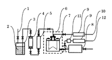
本発明の成膜方法は、第1の構成の成膜方法であっても、第2の構成の成膜方法であっても、例えば図1に示すような気化供給装置及びCVD装置によって行なわれる。
本発明のCVD法による酸化亜鉛膜の成膜において、気化供給装置は、通常は液体マスフローコントローラー等の液体流量制御器5、気化器7、CVD装置8が設置されるほか、必要に応じて脱ガス器4が設けられる。気化器7にはさらに、気体流量制御器9、キャリアガス供給ライン10が接続され、断熱材6が設けられる。また、CVD装置8にはさらに、ガス予熱器11、酸素、オゾン、窒素酸化物、水等の酸化剤ガス供給ライン12が接続される。
The film forming method of the present invention is performed by, for example, a vaporization supply apparatus and a CVD apparatus as shown in FIG. 1 regardless of whether the film forming method has the first structure or the second structure. .
In the formation of a zinc oxide film by the CVD method of the present invention, the vaporization supply device is usually provided with a liquid
酸化亜鉛膜の成膜の際には、例えば、気化器内、CVD装置内を所定の温度、圧力に設定した後、原料容器3から不活性ガスの圧力により、原料2が気化器7に供給されて気化され、さらにCVD装置8に供給される。また、酸化剤ガス供給ライン12から酸素等が供給される。本発明においては、減圧CVD法、常圧CVD法のいずれによってでも行なうことができる。成膜の際は、均一性に優れた原料を、均一に気化し、所望の濃度、流量で供給することができるので、各種基板上に高品質の結晶を有する酸化亜鉛膜が得られる。
When forming the zinc oxide film, for example, after setting the inside of the vaporizer and the CVD apparatus at a predetermined temperature and pressure, the raw material 2 is supplied from the raw material container 3 to the
尚、本発明の成膜方法において使用される気化器7としては、特に制限されることはないが、例えば、図2に示すように、原料供給部14の内部が、フッ素系樹脂、ポリイミド系樹脂等の耐腐食性合成樹脂17で構成される気化器、気化室13に液体原料を噴出して気化させるための噴出管18が、液体原料を噴出する内管とキャリアガスを噴出する外管からなる二重構造の噴出管である気化器、あるいは、CVD原料供給部の側面部に冷却水を流す手段19を有する気化器等を挙げることができる。
The
また、CVD装置としては、第1の構成の成膜方法においては特に制限されることはないが、第2の構成の成膜方法においては、ジメチル亜鉛またはジエチル亜鉛の気化ガスと、酸化剤ガスを含むガスが、直接的に接触しないように、交互に基板表面に供給できる構成である必要がある。
本発明の第2の構成の成膜方法においては、通常は膜厚が5〜500nm成長する毎に、好ましくは膜厚が10〜100nm成長する毎に、ジメチル亜鉛またはジエチル亜鉛の気化ガスと、酸化剤ガスを含むガスの切替えが行なわれる。このようなガスの切替えは、通常は5秒〜10分間隔である。
Further, the CVD apparatus is not particularly limited in the film forming method of the first structure, but in the film forming method of the second structure, a vaporized gas of dimethyl zinc or diethyl zinc and an oxidant gas are used. It is necessary that the gas containing the gas can be alternately supplied to the substrate surface so as not to be in direct contact.
In the film forming method of the second configuration of the present invention, a vaporized gas of dimethylzinc or diethylzinc is usually used every time the film thickness grows from 5 to 500 nm, preferably every 10 to 100 nm. The gas containing the oxidant gas is switched. Such gas switching is usually at intervals of 5 seconds to 10 minutes.
また、第2の構成の成膜方法においては、酸化亜鉛膜の形成を効率よく行なうために、基板の温度を、酸化剤ガスのCVD装置への供給時に、酸化剤ガスの非供給時よりも低く設定することが好ましい。ジメチル亜鉛またはジエチル亜鉛の気化ガスを供給する際の基板の温度は、通常は150〜500℃であり、酸化剤ガスを供給する際の基板の温度は、通常は100〜300℃である。 Further, in the film forming method of the second configuration, in order to efficiently form the zinc oxide film, the temperature of the substrate is set at the time of supplying the oxidizing gas to the CVD apparatus more than when the oxidizing gas is not supplied. It is preferable to set it low. The temperature of the substrate when supplying the vaporized gas of dimethylzinc or diethylzinc is usually 150 to 500 ° C., and the temperature of the substrate when supplying the oxidizing gas is usually 100 to 300 ° C.
次に、本発明を実施例により具体的に説明するが、本発明がこれらにより限定されるものではない。 EXAMPLES Next, although an Example demonstrates this invention concretely, this invention is not limited by these.
(原料の調製)
内径8cm、高さ10cmのステンレス鋼(SUS316)製の容器に、不活性ガス供給ラインからアルゴンを供給して、容器の内部をアルゴン雰囲気にした。次に、この容器に、ジメチル亜鉛及びヘキサンを投入してこれらを混合し、25℃、常圧の状態で撹拌して原料(ジメチル亜鉛の含有量:0.5mol/L)を調製した。
(Preparation of raw materials)
Argon was supplied from an inert gas supply line to a stainless steel (SUS316) container having an inner diameter of 8 cm and a height of 10 cm to make the inside of the container an argon atmosphere. Next, dimethylzinc and hexane were added to the container, mixed, and stirred at 25 ° C. and normal pressure to prepare a raw material (dimethylzinc content: 0.5 mol / L).
(気化器の製作)
内部がフッ素系合成樹脂(PFA)で構成され、気化器外部との接触部がステンレス鋼(SUS316)で構成される原料供給部14を製作した。フッ素系合成樹脂の構成部17は、外径16mm、高さ34.2mmの円柱状であり、その外側のステンレス鋼の厚みは2.0mmである。また、先端が二重構造であり、内管が原料の流路、外管がキャリアガスの流路である噴出管18を設けた。また、原料供給部の側面には、冷却水を流してCVD原料供給部を冷却することができる冷却管19を設けた。
前記の原料供給部14のほか、気化ガス排出口15、ヒーター16を有する図2に示すようなステンレス製(SUS316)の気化器7を製作した。尚、気化室14は、内径が65mm、高さが92.5mmの円柱状で、底部の突起は高さ27.5mmであり、また気化ガス排出口15は底部から15mmの高さに設けた。
(Production of vaporizer)
A raw
In addition to the raw
(気化供給装置の製作)
前記の気化器7、CVD装置8を、脱ガス器4、液体マスフローコントローラー5、キャリアガス供給ライン10、酸化剤ガス供給ライン12、ガス予熱器11、気体流量制御器9等と接続し、断熱材6を設けて、図1に示すような気化供給装置を製作した。尚、酸化剤ガス供給ライン12は、CVD装置の内部で酸化剤ガスが添加されるように設定した。次に、実施例1の原料が充填された原料容器を接続した。
(Production of vaporization supply device)
The
(酸化亜鉛膜の形成)
前記の原料、気化供給装置を使用して、CVD法により、直径20mmのシリコン基板上に、酸化亜鉛膜を以下のようにして成膜した。
気化供給装置内、CVD装置内にアルゴンを供給した後、気化器内を70℃、常圧にするとともに、CVD装置内を40kPa、基板を200℃に保持した。次に、前記の原料を、液体マスフローコントローラーを用いて、0.5g/minの流量で気化器に供給するとともに、キャリアガス供給ラインから70℃に加熱されたアルゴンを、500ml/minの流量で気化器に供給して、原料を気化させCVD装置に供給した。また、30℃の酸素を350ml/minの流量でCVD装置に供給した。
(Formation of zinc oxide film)
A zinc oxide film was formed on a silicon substrate having a diameter of 20 mm by the CVD method using the raw material and the vaporization supply apparatus as follows.
After supplying argon into the vaporization supply apparatus and the CVD apparatus, the vaporizer was set at 70 ° C. and normal pressure, the CVD apparatus was maintained at 40 kPa, and the substrate was maintained at 200 ° C. Next, the raw material is supplied to the vaporizer at a flow rate of 0.5 g / min using a liquid mass flow controller, and argon heated to 70 ° C. from the carrier gas supply line is supplied at a flow rate of 500 ml / min. The raw material was vaporized and supplied to the CVD apparatus. Further, oxygen at 30 ° C. was supplied to the CVD apparatus at a flow rate of 350 ml / min.
(酸化亜鉛膜の評価)
このようにして得られた酸化亜鉛膜を、原子間力顕微鏡により分析した結果、膜厚は0.1μmであり、高純度で均一な酸化亜鉛膜が得られていることが確認された。
(Evaluation of zinc oxide film)
As a result of analyzing the zinc oxide film thus obtained with an atomic force microscope, it was confirmed that the film thickness was 0.1 μm, and a highly pure and uniform zinc oxide film was obtained.
(酸化亜鉛膜の形成)
ジメチル亜鉛を原料として用い、実施例1と同様の気化供給装置を使用して、CVD法により、直径20mmのシリコン基板上に、酸化亜鉛膜を以下のようにして成膜した。
気化供給装置内、CVD装置内にアルゴンを供給した後、気化器内を50℃、常圧にするとともに、CVD装置内を40kPa、基板を200℃に保持した。次に、前記の原料を、液体マスフローコントローラーを用いて、0.01g/minの流量で気化器に供給するとともに、キャリアガス供給ラインから50℃に加熱されたアルゴンを、100ml/minの流量で気化器に供給して、原料を気化させCVD装置に1分間供給した。その後、原料の供給を中断するとともに、基板の温度を120℃に下げ、30℃の酸素を200ml/minの流量でCVD装置に1分間供給した。続いて、酸素の供給を中断するとともに、再度基板の温度を200℃に上げ、原料をCVD装置に1分間供給した。以上の操作を10回繰返して酸化亜鉛膜の成膜を終了した。
(Formation of zinc oxide film)
A zinc oxide film was formed as follows on a silicon substrate having a diameter of 20 mm by a CVD method using dimethyl zinc as a raw material and using the same vaporization supply apparatus as in Example 1.
After supplying argon into the vaporization supply apparatus and the CVD apparatus, the vaporizer was set at 50 ° C. and normal pressure, the CVD apparatus was maintained at 40 kPa, and the substrate was maintained at 200 ° C. Next, the raw material is supplied to the vaporizer at a flow rate of 0.01 g / min using a liquid mass flow controller, and argon heated to 50 ° C. from the carrier gas supply line is supplied at a flow rate of 100 ml / min. The material was supplied to the vaporizer to vaporize the raw material and supplied to the CVD apparatus for 1 minute. Thereafter, the supply of the raw materials was interrupted, the temperature of the substrate was lowered to 120 ° C., and oxygen at 30 ° C. was supplied to the CVD apparatus at a flow rate of 200 ml / min for 1 minute. Subsequently, the supply of oxygen was interrupted, the temperature of the substrate was raised again to 200 ° C., and the raw material was supplied to the CVD apparatus for 1 minute. The above operation was repeated 10 times to complete the formation of the zinc oxide film.
(酸化亜鉛膜の評価)
このようにして得られた酸化亜鉛膜を、原子間力顕微鏡により分析した結果、膜厚は0.15μmであり、高純度で均一な酸化亜鉛膜が得られていることが確認された。
(Evaluation of zinc oxide film)
The zinc oxide film thus obtained was analyzed by an atomic force microscope. As a result, the film thickness was 0.15 μm, and it was confirmed that a highly pure and uniform zinc oxide film was obtained.
(酸化亜鉛膜の形成)
実施例1の原料を用い、実施例1と同様の気化供給装置を使用して、CVD法により、直径20mmのサファイア基板上に、酸化亜鉛膜を以下のようにして成膜した。
気化供給装置内、CVD装置内にアルゴンを供給した後、気化器内を70℃、常圧にするとともに、CVD装置内を40kPa、基板を200℃に保持した。次に、実施例1の原料を、液体マスフローコントローラーを用いて、0.5g/minの流量で気化器に供給するとともに、キャリアガス供給ラインから70℃に加熱されたアルゴンを、500ml/minの流量で気化器に供給して、原料を気化させCVD装置に1分間供給した。その後、原料の供給を中断するとともに、基板の温度を120℃に下げ、30℃の酸素を350ml/minの流量でCVD装置に1分間供給した。続いて、酸素の供給を中断するとともに、再度基板の温度を200℃に上げ、原料をCVD装置に1分間供給した。以上の操作を10回繰返して酸化亜鉛膜の成膜を終了した。
(Formation of zinc oxide film)
A zinc oxide film was formed as follows on a sapphire substrate having a diameter of 20 mm by a CVD method using the same vaporization supply apparatus as in Example 1 using the raw material of Example 1.
After supplying argon into the vaporization supply apparatus and the CVD apparatus, the vaporizer was set at 70 ° C. and normal pressure, the CVD apparatus was maintained at 40 kPa, and the substrate was maintained at 200 ° C. Next, the raw material of Example 1 was supplied to the vaporizer at a flow rate of 0.5 g / min using a liquid mass flow controller, and argon heated to 70 ° C. from the carrier gas supply line was supplied at 500 ml / min. The raw material was vaporized by supplying it to the vaporizer at a flow rate and supplied to the CVD apparatus for 1 minute. Thereafter, the supply of the raw materials was interrupted, the temperature of the substrate was lowered to 120 ° C., and oxygen at 30 ° C. was supplied to the CVD apparatus at a flow rate of 350 ml / min for 1 minute. Subsequently, the supply of oxygen was interrupted, the temperature of the substrate was raised again to 200 ° C., and the raw material was supplied to the CVD apparatus for 1 minute. The above operation was repeated 10 times to complete the formation of the zinc oxide film.
(酸化亜鉛膜の評価)
このようにして得られた酸化亜鉛膜を、原子間力顕微鏡により分析した結果、膜厚は0.18μmであり、高純度で均一な酸化亜鉛膜が得られていることが確認された。
(Evaluation of zinc oxide film)
As a result of analyzing the thus obtained zinc oxide film with an atomic force microscope, it was confirmed that the film thickness was 0.18 μm, and a highly pure and uniform zinc oxide film was obtained.
1 不活性ガス供給ライン
2 原料
3 原料容器
4 脱ガス器
5 液体流量制御器
6 断熱材
7 気化器
8 CVD装置
9 気体流量制御器
10 キャリアガス供給ライン
11 ガス予熱器
12 酸化剤ガス供給ライン
13 気化室
14 原料供給部
15 気化ガス排出口
16 ヒーター
17 合成樹脂構成部
18 二重構造の噴出管
19 冷却管
DESCRIPTION OF
Claims (7)
Priority Applications (7)
| Application Number | Priority Date | Filing Date | Title |
|---|---|---|---|
| JP2005161187A JP4699092B2 (en) | 2005-06-01 | 2005-06-01 | Method for forming zinc oxide film |
| US11/434,072 US20060275948A1 (en) | 2005-06-01 | 2006-05-16 | Process for forming zinc oxide film |
| EP06010939A EP1728893B1 (en) | 2005-06-01 | 2006-05-26 | Process for forming zinc oxide film |
| DE602006021256T DE602006021256D1 (en) | 2005-06-01 | 2006-05-26 | |
| KR1020060048332A KR20060125500A (en) | 2005-06-01 | 2006-05-29 | Process for forming zinc oxide film |
| CNA2006100806988A CN1873051A (en) | 2005-06-01 | 2006-05-29 | Process for forming zinc oxide film |
| TW095118928A TWI332531B (en) | 2005-06-01 | 2006-05-29 | Process for forming zinc oxide film |
Applications Claiming Priority (1)
| Application Number | Priority Date | Filing Date | Title |
|---|---|---|---|
| JP2005161187A JP4699092B2 (en) | 2005-06-01 | 2005-06-01 | Method for forming zinc oxide film |
Publications (2)
| Publication Number | Publication Date |
|---|---|
| JP2006336062A JP2006336062A (en) | 2006-12-14 |
| JP4699092B2 true JP4699092B2 (en) | 2011-06-08 |
Family
ID=36928153
Family Applications (1)
| Application Number | Title | Priority Date | Filing Date |
|---|---|---|---|
| JP2005161187A Expired - Fee Related JP4699092B2 (en) | 2005-06-01 | 2005-06-01 | Method for forming zinc oxide film |
Country Status (7)
| Country | Link |
|---|---|
| US (1) | US20060275948A1 (en) |
| EP (1) | EP1728893B1 (en) |
| JP (1) | JP4699092B2 (en) |
| KR (1) | KR20060125500A (en) |
| CN (1) | CN1873051A (en) |
| DE (1) | DE602006021256D1 (en) |
| TW (1) | TWI332531B (en) |
Families Citing this family (20)
| Publication number | Priority date | Publication date | Assignee | Title |
|---|---|---|---|---|
| GB0518383D0 (en) * | 2005-09-09 | 2005-10-19 | Pilkington Plc | Deposition process |
| WO2008007770A1 (en) * | 2006-07-14 | 2008-01-17 | Dai Nippon Printing Co., Ltd. | Transparent conducting layer coated film and its use |
| US7491575B2 (en) * | 2006-08-02 | 2009-02-17 | Xerox Corporation | Fabricating zinc oxide semiconductor using hydrolysis |
| JP4616359B2 (en) * | 2007-01-09 | 2011-01-19 | 韓國電子通信研究院 | Method for forming ZnO semiconductor film for electronic device and thin film transistor including the semiconductor film |
| KR100966081B1 (en) * | 2008-01-03 | 2010-06-25 | 아주대학교산학협력단 | Method of forming ZnO thin-film and Method of forming thin-film transistor using the same |
| JP5200551B2 (en) * | 2008-01-18 | 2013-06-05 | 東京エレクトロン株式会社 | Vaporized raw material supply apparatus, film forming apparatus, and vaporized raw material supply method |
| WO2010035312A1 (en) | 2008-09-24 | 2010-04-01 | 東芝三菱電機産業システム株式会社 | METHOD FOR PRODUCTION OF ZINC OXIDE (ZnO) FILM OR MAGNESIUM ZINC OXIDE (ZnMgO) FILM, AND APPARATUS FOR PRODUCTION OF ZINC OXIDE FILM OR MAGNESIUM ZINC OXIDE FILM |
| JP5674186B2 (en) * | 2010-02-16 | 2015-02-25 | 国立大学法人 宮崎大学 | Zinc oxide thin film production method, and antistatic thin film, ultraviolet cut thin film, transparent electrode thin film produced by this method |
| TWI465401B (en) * | 2009-04-21 | 2014-12-21 | Tosoh Finechem Corp | "dope or undoped zinc oxide thin film manufacturing method and a method for producing the zinc oxide thin film using the same |
| JP5515144B2 (en) * | 2009-05-12 | 2014-06-11 | 東ソー・ファインケム株式会社 | Composition for forming doped zinc oxide thin film and method for producing doped zinc oxide thin film |
| US9096441B2 (en) | 2009-04-21 | 2015-08-04 | Tosoh Finechem Corporation | Composition for manufacturing doped or undoped zinc oxide thin film and method for manufacturing zinc oxide thin film using same |
| WO2010131621A1 (en) * | 2009-05-12 | 2010-11-18 | 国立大学法人 宮崎大学 | Composition for production of doped zinc oxide thin film, process for production of zinc oxide thin film, antistatic thin film, ultraviolet ray blocking thin film, and transparent electrode thin film |
| US20120225320A1 (en) * | 2009-10-15 | 2012-09-06 | Arkema Inc. | DEPOSITION OF DOPED ZnO FILMS ON POLYMER SUBSTRATES BY UV-ASSISTED CHEMICAL VAPOR DEPOSITION |
| DE102012203212A1 (en) * | 2012-03-01 | 2013-09-05 | Osram Opto Semiconductors Gmbh | Coating system useful for producing layer on substrate using growth process, preferably for performing atomic layer deposition, comprises supply container, in which liquid starting material for layer is provided, and evaporator unit |
| EP2825687B1 (en) * | 2012-03-16 | 2020-08-19 | Pilkington Group Limited | Chemical vapor deposition process for depositing zinc oxide coatings |
| KR20140046617A (en) * | 2012-10-09 | 2014-04-21 | 삼성코닝정밀소재 주식회사 | Zinc oxide precursor and method of depositing zinc oxide-based thin film using the same |
| KR101466842B1 (en) * | 2012-11-28 | 2014-11-28 | 코닝정밀소재 주식회사 | Method of fabricating zinc oxide based thin film for transparent electrode |
| KR20150019623A (en) * | 2013-08-14 | 2015-02-25 | 코닝정밀소재 주식회사 | Method of depositing zinc oxide based thin film |
| JP6564994B2 (en) * | 2015-08-26 | 2019-08-28 | 株式会社アルバック | Antibacterial member forming method and antibacterial member |
| EP3715499A1 (en) * | 2019-03-29 | 2020-09-30 | Picosun Oy | Substrate coating |
Citations (3)
| Publication number | Priority date | Publication date | Assignee | Title |
|---|---|---|---|---|
| JPS62284078A (en) * | 1987-05-22 | 1987-12-09 | Oki Electric Ind Co Ltd | Chemical vapor growth method |
| JPH04280975A (en) * | 1991-03-11 | 1992-10-06 | Makoto Konagai | Production of zno transparent conductive film |
| JP2006124834A (en) * | 2004-10-29 | 2006-05-18 | Sharp Corp | ZnO SEED LAYER BY ALD FOR DEPOSITING ZnO NANOSTRUCTURE ON SILICON SUBSTRATE |
Family Cites Families (8)
| Publication number | Priority date | Publication date | Assignee | Title |
|---|---|---|---|---|
| JPH0682625B2 (en) * | 1985-06-04 | 1994-10-19 | シーメンス ソーラー インダストリーズ,エル.ピー. | Deposition method of zinc oxide film |
| US5126921A (en) * | 1990-07-06 | 1992-06-30 | Akira Fujishima | Electronic component and a method for manufacturing the same |
| AU650782B2 (en) * | 1991-09-24 | 1994-06-30 | Canon Kabushiki Kaisha | Solar cell |
| US6258170B1 (en) * | 1997-09-11 | 2001-07-10 | Applied Materials, Inc. | Vaporization and deposition apparatus |
| JP3394488B2 (en) | 2000-01-24 | 2003-04-07 | 星和電機株式会社 | Gallium nitride based semiconductor light emitting device and method of manufacturing the same |
| US7368014B2 (en) * | 2001-08-09 | 2008-05-06 | Micron Technology, Inc. | Variable temperature deposition methods |
| KR20030025354A (en) | 2001-09-20 | 2003-03-29 | 한국과학기술연구원 | Fabrication method of blue light emitting ZnO thin film phosphor |
| JP2004323941A (en) | 2003-04-25 | 2004-11-18 | Central Glass Co Ltd | Method of depositing zinc oxide film |
-
2005
- 2005-06-01 JP JP2005161187A patent/JP4699092B2/en not_active Expired - Fee Related
-
2006
- 2006-05-16 US US11/434,072 patent/US20060275948A1/en not_active Abandoned
- 2006-05-26 DE DE602006021256T patent/DE602006021256D1/de active Active
- 2006-05-26 EP EP06010939A patent/EP1728893B1/en not_active Expired - Fee Related
- 2006-05-29 TW TW095118928A patent/TWI332531B/en not_active IP Right Cessation
- 2006-05-29 CN CNA2006100806988A patent/CN1873051A/en active Pending
- 2006-05-29 KR KR1020060048332A patent/KR20060125500A/en not_active Application Discontinuation
Patent Citations (3)
| Publication number | Priority date | Publication date | Assignee | Title |
|---|---|---|---|---|
| JPS62284078A (en) * | 1987-05-22 | 1987-12-09 | Oki Electric Ind Co Ltd | Chemical vapor growth method |
| JPH04280975A (en) * | 1991-03-11 | 1992-10-06 | Makoto Konagai | Production of zno transparent conductive film |
| JP2006124834A (en) * | 2004-10-29 | 2006-05-18 | Sharp Corp | ZnO SEED LAYER BY ALD FOR DEPOSITING ZnO NANOSTRUCTURE ON SILICON SUBSTRATE |
Also Published As
| Publication number | Publication date |
|---|---|
| US20060275948A1 (en) | 2006-12-07 |
| TW200704818A (en) | 2007-02-01 |
| EP1728893B1 (en) | 2011-04-13 |
| DE602006021256D1 (en) | 2011-05-26 |
| CN1873051A (en) | 2006-12-06 |
| EP1728893A2 (en) | 2006-12-06 |
| TWI332531B (en) | 2010-11-01 |
| JP2006336062A (en) | 2006-12-14 |
| KR20060125500A (en) | 2006-12-06 |
| EP1728893A3 (en) | 2007-09-05 |
Similar Documents
| Publication | Publication Date | Title |
|---|---|---|
| JP4699092B2 (en) | Method for forming zinc oxide film | |
| US20030092262A1 (en) | Solvated ruthenium precursors for direct liquid injection of ruthenium and ruthenium oxide | |
| FR2880036A1 (en) | Deposition of silver or silver alloy nanoparticles on substrate comprises use of organometallic precursors and deposition carried out in presence of reactive oxidant gas | |
| US3701682A (en) | Thin film deposition system | |
| CN104755485A (en) | Aluminum compound, thin film-forming raw material, and method for producing thin film | |
| ES2360199T3 (en) | SUITABLE REDUCED ORGANOMETAL COMPLEXES OF REDACTED REACTIVITY FOR USE IN THE CHEMICAL DEPOSITION IN VAPOR PHASE OF METAL OXIDE FILMS. | |
| JP3896594B2 (en) | Vaporizer for CVD, solution vaporization type CVD apparatus, and vaporization method for CVD | |
| JP4508702B2 (en) | Deposition method | |
| JP6213173B2 (en) | Method for producing titanium oxide film and titanium oxide film | |
| JP2009536144A (en) | Method for depositing a zinc oxide coating on a substrate | |
| US5381755A (en) | Method of synthesizing high quality, doped diamond and diamonds and devices obtained therefrom | |
| JP2007239083A (en) | Method for forming film of metal oxide on surface of substrate, and nozzle of air-open-type cvd apparatus used in the method | |
| JP2007246343A (en) | Crystal production apparatus | |
| KR20050041888A (en) | Material for forming insulation film and film-forming method with the use of the material | |
| WO2020191837A1 (en) | Spray pyrolysis preparation method for gradient self-doping multi-element metal oxide semiconductor film | |
| US20110175207A1 (en) | Method for producing metal oxide layers | |
| JP4688458B2 (en) | Insulating film forming material and film forming method using the same | |
| JP2000000444A (en) | Alcohol vapor stop-off film in gas phase | |
| JP4107923B2 (en) | Method for producing yttrium-containing composite oxide thin film | |
| JP2006303534A (en) | Vaporizer for cvd, solution vaporizing cvd apparatus and vaporization method for cvd | |
| US20120071001A1 (en) | Vaporizing and feed apparatus and vaporizing and feed method | |
| JP4419526B2 (en) | Evaluation method of vaporizer performance | |
| CA2355692C (en) | Method for forming a metal alloy coating such as mcraly | |
| JP2568224B2 (en) | Gas-phase chemical reaction material supply method | |
| RU2397572C1 (en) | Method of obtaining film coatings of tin oxide on substrates |
Legal Events
| Date | Code | Title | Description |
|---|---|---|---|
| A621 | Written request for application examination |
Free format text: JAPANESE INTERMEDIATE CODE: A621 Effective date: 20071217 |
|
| A977 | Report on retrieval |
Free format text: JAPANESE INTERMEDIATE CODE: A971007 Effective date: 20100412 |
|
| A131 | Notification of reasons for refusal |
Free format text: JAPANESE INTERMEDIATE CODE: A131 Effective date: 20101220 |
|
| A521 | Request for written amendment filed |
Free format text: JAPANESE INTERMEDIATE CODE: A523 Effective date: 20110204 |
|
| A01 | Written decision to grant a patent or to grant a registration (utility model) |
Free format text: JAPANESE INTERMEDIATE CODE: A01 Effective date: 20110228 |
|
| A61 | First payment of annual fees (during grant procedure) |
Free format text: JAPANESE INTERMEDIATE CODE: A61 Effective date: 20110302 |
|
| LAPS | Cancellation because of no payment of annual fees |