JP4690938B2 - High frequency element module - Google Patents
High frequency element module Download PDFInfo
- Publication number
- JP4690938B2 JP4690938B2 JP2006136290A JP2006136290A JP4690938B2 JP 4690938 B2 JP4690938 B2 JP 4690938B2 JP 2006136290 A JP2006136290 A JP 2006136290A JP 2006136290 A JP2006136290 A JP 2006136290A JP 4690938 B2 JP4690938 B2 JP 4690938B2
- Authority
- JP
- Japan
- Prior art keywords
- frequency element
- substrate
- potting material
- frequency
- polyimide
- Prior art date
- Legal status (The legal status is an assumption and is not a legal conclusion. Google has not performed a legal analysis and makes no representation as to the accuracy of the status listed.)
- Expired - Fee Related
Links
Images


Classifications
-
- H—ELECTRICITY
- H01—ELECTRIC ELEMENTS
- H01L—SEMICONDUCTOR DEVICES NOT COVERED BY CLASS H10
- H01L23/00—Details of semiconductor or other solid state devices
- H01L23/28—Encapsulations, e.g. encapsulating layers, coatings, e.g. for protection
- H01L23/31—Encapsulations, e.g. encapsulating layers, coatings, e.g. for protection characterised by the arrangement or shape
- H01L23/3107—Encapsulations, e.g. encapsulating layers, coatings, e.g. for protection characterised by the arrangement or shape the device being completely enclosed
-
- H—ELECTRICITY
- H01—ELECTRIC ELEMENTS
- H01L—SEMICONDUCTOR DEVICES NOT COVERED BY CLASS H10
- H01L23/00—Details of semiconductor or other solid state devices
-
- H—ELECTRICITY
- H01—ELECTRIC ELEMENTS
- H01L—SEMICONDUCTOR DEVICES NOT COVERED BY CLASS H10
- H01L23/00—Details of semiconductor or other solid state devices
- H01L23/28—Encapsulations, e.g. encapsulating layers, coatings, e.g. for protection
-
- H—ELECTRICITY
- H01—ELECTRIC ELEMENTS
- H01L—SEMICONDUCTOR DEVICES NOT COVERED BY CLASS H10
- H01L23/00—Details of semiconductor or other solid state devices
- H01L23/28—Encapsulations, e.g. encapsulating layers, coatings, e.g. for protection
- H01L23/29—Encapsulations, e.g. encapsulating layers, coatings, e.g. for protection characterised by the material, e.g. carbon
-
- H—ELECTRICITY
- H01—ELECTRIC ELEMENTS
- H01L—SEMICONDUCTOR DEVICES NOT COVERED BY CLASS H10
- H01L23/00—Details of semiconductor or other solid state devices
- H01L23/552—Protection against radiation, e.g. light or electromagnetic waves
-
- H—ELECTRICITY
- H01—ELECTRIC ELEMENTS
- H01L—SEMICONDUCTOR DEVICES NOT COVERED BY CLASS H10
- H01L23/00—Details of semiconductor or other solid state devices
- H01L23/58—Structural electrical arrangements for semiconductor devices not otherwise provided for, e.g. in combination with batteries
- H01L23/64—Impedance arrangements
- H01L23/66—High-frequency adaptations
-
- H—ELECTRICITY
- H05—ELECTRIC TECHNIQUES NOT OTHERWISE PROVIDED FOR
- H05K—PRINTED CIRCUITS; CASINGS OR CONSTRUCTIONAL DETAILS OF ELECTRIC APPARATUS; MANUFACTURE OF ASSEMBLAGES OF ELECTRICAL COMPONENTS
- H05K9/00—Screening of apparatus or components against electric or magnetic fields
-
- H—ELECTRICITY
- H01—ELECTRIC ELEMENTS
- H01L—SEMICONDUCTOR DEVICES NOT COVERED BY CLASS H10
- H01L2224/00—Indexing scheme for arrangements for connecting or disconnecting semiconductor or solid-state bodies and methods related thereto as covered by H01L24/00
- H01L2224/01—Means for bonding being attached to, or being formed on, the surface to be connected, e.g. chip-to-package, die-attach, "first-level" interconnects; Manufacturing methods related thereto
- H01L2224/42—Wire connectors; Manufacturing methods related thereto
- H01L2224/44—Structure, shape, material or disposition of the wire connectors prior to the connecting process
- H01L2224/45—Structure, shape, material or disposition of the wire connectors prior to the connecting process of an individual wire connector
- H01L2224/45001—Core members of the connector
- H01L2224/45099—Material
- H01L2224/451—Material with a principal constituent of the material being a metal or a metalloid, e.g. boron (B), silicon (Si), germanium (Ge), arsenic (As), antimony (Sb), tellurium (Te) and polonium (Po), and alloys thereof
- H01L2224/45138—Material with a principal constituent of the material being a metal or a metalloid, e.g. boron (B), silicon (Si), germanium (Ge), arsenic (As), antimony (Sb), tellurium (Te) and polonium (Po), and alloys thereof the principal constituent melting at a temperature of greater than or equal to 950°C and less than 1550°C
- H01L2224/45144—Gold (Au) as principal constituent
-
- H—ELECTRICITY
- H01—ELECTRIC ELEMENTS
- H01L—SEMICONDUCTOR DEVICES NOT COVERED BY CLASS H10
- H01L2224/00—Indexing scheme for arrangements for connecting or disconnecting semiconductor or solid-state bodies and methods related thereto as covered by H01L24/00
- H01L2224/01—Means for bonding being attached to, or being formed on, the surface to be connected, e.g. chip-to-package, die-attach, "first-level" interconnects; Manufacturing methods related thereto
- H01L2224/42—Wire connectors; Manufacturing methods related thereto
- H01L2224/47—Structure, shape, material or disposition of the wire connectors after the connecting process
- H01L2224/48—Structure, shape, material or disposition of the wire connectors after the connecting process of an individual wire connector
- H01L2224/4805—Shape
- H01L2224/4809—Loop shape
- H01L2224/48091—Arched
-
- H—ELECTRICITY
- H01—ELECTRIC ELEMENTS
- H01L—SEMICONDUCTOR DEVICES NOT COVERED BY CLASS H10
- H01L2224/00—Indexing scheme for arrangements for connecting or disconnecting semiconductor or solid-state bodies and methods related thereto as covered by H01L24/00
- H01L2224/01—Means for bonding being attached to, or being formed on, the surface to be connected, e.g. chip-to-package, die-attach, "first-level" interconnects; Manufacturing methods related thereto
- H01L2224/42—Wire connectors; Manufacturing methods related thereto
- H01L2224/47—Structure, shape, material or disposition of the wire connectors after the connecting process
- H01L2224/48—Structure, shape, material or disposition of the wire connectors after the connecting process of an individual wire connector
- H01L2224/481—Disposition
- H01L2224/48151—Connecting between a semiconductor or solid-state body and an item not being a semiconductor or solid-state body, e.g. chip-to-substrate, chip-to-passive
- H01L2224/48221—Connecting between a semiconductor or solid-state body and an item not being a semiconductor or solid-state body, e.g. chip-to-substrate, chip-to-passive the body and the item being stacked
- H01L2224/48225—Connecting between a semiconductor or solid-state body and an item not being a semiconductor or solid-state body, e.g. chip-to-substrate, chip-to-passive the body and the item being stacked the item being non-metallic, e.g. insulating substrate with or without metallisation
- H01L2224/48227—Connecting between a semiconductor or solid-state body and an item not being a semiconductor or solid-state body, e.g. chip-to-substrate, chip-to-passive the body and the item being stacked the item being non-metallic, e.g. insulating substrate with or without metallisation connecting the wire to a bond pad of the item
-
- H—ELECTRICITY
- H01—ELECTRIC ELEMENTS
- H01L—SEMICONDUCTOR DEVICES NOT COVERED BY CLASS H10
- H01L24/00—Arrangements for connecting or disconnecting semiconductor or solid-state bodies; Methods or apparatus related thereto
- H01L24/01—Means for bonding being attached to, or being formed on, the surface to be connected, e.g. chip-to-package, die-attach, "first-level" interconnects; Manufacturing methods related thereto
- H01L24/42—Wire connectors; Manufacturing methods related thereto
- H01L24/44—Structure, shape, material or disposition of the wire connectors prior to the connecting process
- H01L24/45—Structure, shape, material or disposition of the wire connectors prior to the connecting process of an individual wire connector
-
- H—ELECTRICITY
- H01—ELECTRIC ELEMENTS
- H01L—SEMICONDUCTOR DEVICES NOT COVERED BY CLASS H10
- H01L24/00—Arrangements for connecting or disconnecting semiconductor or solid-state bodies; Methods or apparatus related thereto
- H01L24/01—Means for bonding being attached to, or being formed on, the surface to be connected, e.g. chip-to-package, die-attach, "first-level" interconnects; Manufacturing methods related thereto
- H01L24/42—Wire connectors; Manufacturing methods related thereto
- H01L24/47—Structure, shape, material or disposition of the wire connectors after the connecting process
- H01L24/48—Structure, shape, material or disposition of the wire connectors after the connecting process of an individual wire connector
-
- H—ELECTRICITY
- H01—ELECTRIC ELEMENTS
- H01L—SEMICONDUCTOR DEVICES NOT COVERED BY CLASS H10
- H01L2924/00—Indexing scheme for arrangements or methods for connecting or disconnecting semiconductor or solid-state bodies as covered by H01L24/00
- H01L2924/0001—Technical content checked by a classifier
- H01L2924/00014—Technical content checked by a classifier the subject-matter covered by the group, the symbol of which is combined with the symbol of this group, being disclosed without further technical details
-
- H—ELECTRICITY
- H01—ELECTRIC ELEMENTS
- H01L—SEMICONDUCTOR DEVICES NOT COVERED BY CLASS H10
- H01L2924/00—Indexing scheme for arrangements or methods for connecting or disconnecting semiconductor or solid-state bodies as covered by H01L24/00
- H01L2924/01—Chemical elements
- H01L2924/01079—Gold [Au]
-
- H—ELECTRICITY
- H01—ELECTRIC ELEMENTS
- H01L—SEMICONDUCTOR DEVICES NOT COVERED BY CLASS H10
- H01L2924/00—Indexing scheme for arrangements or methods for connecting or disconnecting semiconductor or solid-state bodies as covered by H01L24/00
- H01L2924/10—Details of semiconductor or other solid state devices to be connected
- H01L2924/11—Device type
- H01L2924/13—Discrete devices, e.g. 3 terminal devices
- H01L2924/1304—Transistor
- H01L2924/1306—Field-effect transistor [FET]
-
- H—ELECTRICITY
- H01—ELECTRIC ELEMENTS
- H01L—SEMICONDUCTOR DEVICES NOT COVERED BY CLASS H10
- H01L2924/00—Indexing scheme for arrangements or methods for connecting or disconnecting semiconductor or solid-state bodies as covered by H01L24/00
- H01L2924/10—Details of semiconductor or other solid state devices to be connected
- H01L2924/11—Device type
- H01L2924/14—Integrated circuits
- H01L2924/141—Analog devices
- H01L2924/1423—Monolithic Microwave Integrated Circuit [MMIC]
-
- H—ELECTRICITY
- H01—ELECTRIC ELEMENTS
- H01L—SEMICONDUCTOR DEVICES NOT COVERED BY CLASS H10
- H01L2924/00—Indexing scheme for arrangements or methods for connecting or disconnecting semiconductor or solid-state bodies as covered by H01L24/00
- H01L2924/15—Details of package parts other than the semiconductor or other solid state devices to be connected
- H01L2924/151—Die mounting substrate
- H01L2924/1515—Shape
- H01L2924/15153—Shape the die mounting substrate comprising a recess for hosting the device
-
- H—ELECTRICITY
- H01—ELECTRIC ELEMENTS
- H01L—SEMICONDUCTOR DEVICES NOT COVERED BY CLASS H10
- H01L2924/00—Indexing scheme for arrangements or methods for connecting or disconnecting semiconductor or solid-state bodies as covered by H01L24/00
- H01L2924/15—Details of package parts other than the semiconductor or other solid state devices to be connected
- H01L2924/151—Die mounting substrate
- H01L2924/1517—Multilayer substrate
-
- H—ELECTRICITY
- H01—ELECTRIC ELEMENTS
- H01L—SEMICONDUCTOR DEVICES NOT COVERED BY CLASS H10
- H01L2924/00—Indexing scheme for arrangements or methods for connecting or disconnecting semiconductor or solid-state bodies as covered by H01L24/00
- H01L2924/30—Technical effects
- H01L2924/301—Electrical effects
- H01L2924/3025—Electromagnetic shielding
Description
本発明は、マイクロ波素子などの高周波素子を埋め込んだ高周波素子モジュールに係り、特にその構造に関する。 The present invention relates to a high-frequency element module in which a high-frequency element such as a microwave element is embedded, and more particularly to its structure.
最近の情報化社会の進展に伴い伝送容量の増大の要求はますます強まっており、より伝送容量の大きいシステムや高度な変調方式が求められるようになってきた。これに伴って高い利得を有ししかも低価格のデバイスが求められている。 With the recent development of the information society, the demand for an increase in transmission capacity has been increasing, and a system with a larger transmission capacity and an advanced modulation method have been demanded. Accordingly, there is a demand for a device having a high gain and a low price.
このような要求に対して、セラミックの単板に金属プレートを備え素子を固着した簡易型パッケージにポリイミドを塗布して表面を保護し、その上にワイヤや素子を保護するためのポッティング材を塗布したモジュールが知られている(例えば、特許文献1参照)。 In response to such demands, polyimide is applied to a simple package that has a metal plate on a ceramic single plate and the elements are fixed to protect the surface, and a potting material for protecting the wires and elements is applied thereon. A known module is known (for example, see Patent Document 1).
しかし、ポッティング材は絶縁性を有するが、高性能の素子や高利得の素子では電磁界が放射され、外部に悪影響を及ぼしたり、逆に周囲の電磁界や自己が発するマイクロ波の出力の回りこみによって、著しく性能を劣化させるので、用途が限定される場合がある。
本発明は上記のような従来の高周波素子モジュールの問題点にかんがみてなされたもので、電磁波の外部への影響及び外部から影響が少なくしたがって電気的性能がよく、構造が簡単でしかも廉価な高周波素子モジュールを提供することを目的とする。 The present invention has been made in view of the problems of the conventional high-frequency element module as described above, and is less affected by the outside of the electromagnetic wave and less affected by the outside. Therefore, the electrical performance is good, the structure is simple, and the high-frequency is inexpensive. An object is to provide an element module.
本発明の請求項1によれば、表面に電極が設けられ裏面に接地基板が設けられた絶縁基板と、この絶縁基板に設けられ、この素子の端子が前記電極と接続された高周波素子と、この高周波素子に塗布されたポリイミドと、このポリイミドの塗布された前記高周波素子を封止するポッティング材と、このポッティング材の上に設けられ、前記接地基板と接続された金属層と、この金属層を覆うように設けられた絶縁層と、この絶縁層の上に設けられ、前記電極と接続される配線パターンと、この配線パターンの上に設けられた保護層と、を有することを特徴とする高周波素子モジュールを提供する。
According to
本発明によれば、電磁波の外部への影響及び外部から影響が少なくしたがって電気的性能がよく、構造が簡単でしかも廉価な高周波素子モジュールが得られる。 According to the present invention, it is possible to obtain a high-frequency element module that has less influence on the outside of the electromagnetic wave and less influence on the outside, and thus has good electrical performance, a simple structure, and an inexpensive price.
以下、本発明の実施形態について図面を用いて説明する。 Hereinafter, embodiments of the present invention will be described with reference to the drawings.
<第1の実施形態>
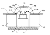
図1は本発明第1の実施形態の高周波素子モジュールの構造を示す断面図であり、図2は、この高周波素子モジュールの上面図である。図1は、図2のA1−A2における断面を表す。
<First Embodiment>
FIG. 1 is a cross-sectional view showing the structure of a high frequency device module according to a first embodiment of the present invention, and FIG. 2 is a top view of the high frequency device module. FIG. 1 shows a cross section taken along line A1-A2 of FIG.
所定の孔部11を有し、セラミックで構成され、表面に配線が設けられた絶縁基板12と、この絶縁基板12の表面に配線された電極13a,13bと、孔部11の裏面を含んで設けられた接地基板13と、この接地基板13上の孔部11内に設けられた台部14と、この台部14の上に固定された高周波素子15と、この高周波素子15の素子端子16a,16bと上記絶縁基板13上の電極13a,13bとを接続する、例えば金で構成されたワイヤ17a,17bと、これらのワイヤ17a,17bや上記高周波素子15の上にかぶせられ封止されるポッティング材18と、このポッティング材18の上に設けられた金属膜19とから成っている。高周波素子15は例えば電界効果トランジスタ(FET)であり、その周囲には、この素子の表面を保護し密着性をよくするために例えばポリイミド20が塗布される。
Insulating
次にこの実施形態の高周波素子モジュールの製造方法について述べる。ポッティング材18を設けるまでは従来と同じ方法でよい。次に図3に示すように、ポッティング材18の上部の必要な部分のみを空けたマスクパターン31を設けてこのマスクパターンにより金属材料、例えばアルミニウムを蒸着させることにより金属膜19を設ける。金属膜19の厚さは、1〜5ミクロン程度とすることが好ましい。
Next, a method for manufacturing the high frequency device module of this embodiment will be described. Until the
また、金属膜19は、図2に示すような大きさ、形状とする。すなわち、図1に示す断面とは直交するする方向の絶縁基板12上において、図2に示されるように接地端子22a,22bが設けられており、ポッティング材18上の金属膜19は、これらの接地端子22a,22bに接続されるような形状とする。接地端子22a,22bは上記接地基板13と接続されている。
The
一方、絶縁基板12の孔部11に電極13a,13bも含めてポッティング材18により覆われているが、この上の金属膜19は上記電極13a,13bに接触しないように設けられる。金属膜19をこのような大きさ、形状とすることにより、金属膜19と接地端子22a,22bが接続され、電磁遮蔽されることになる。
On the other hand, the
金属膜としてアルミニウムを用いれば遮蔽効果も高く、廉価な高周波素子モジュールが得られる。 If aluminum is used as the metal film, the shielding effect is high and an inexpensive high-frequency element module can be obtained.
この実施形態によれば、高周波素子15をほぼ完全に電磁シールでき、外部の影響を少なくすることができる。しかもアイソレーションが向上するので高利得の高周波素子を取り扱うことができ、廉価な高周波素子モジュールが得られる。
According to this embodiment, the high-
<第2の実施形態>
ところで、上記の高周波素子として用いられるモノリシックマイクロ波集積回路(MMIC;Monolithic Microwave Integrated circuits)素子などでは、小型化の要求からモジュールの端子位置を変更することが頻繁に行われるようになっている。このような場合、ボンディングワイヤを変更することも考えられるが、MMIC素子など高利得のデバイスでは、上記高周波素子の上をワイヤがまたぐ形になると、デバイスで発生した電磁界の誘導を拾って発振するなどの不具合を生ずる場合がある。次に述べる第2の実施形態は、このような場合に適する高周波素子モジュールである。
<Second Embodiment>
By the way, in a monolithic microwave integrated circuit (MMIC) element used as the high-frequency element, the terminal position of the module is frequently changed due to a demand for miniaturization. In such a case, it is possible to change the bonding wire. However, in a high gain device such as an MMIC element, when the wire crosses over the high frequency element, it picks up the induction of the electromagnetic field generated by the device and oscillates. May cause problems such as A second embodiment described below is a high-frequency element module suitable for such a case.
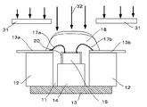
図4は、この第2の実施形態の高周波素子モジュールの構造を示す断面図である。番号41〜50は図1に示す番号11〜20に対応する。例えばセラミックで構成された絶縁基板42の孔部41に台部41が設けられこの上に、例えばMMIC素子である高周波素子45がマウントされ、裏面は接地基板43が設けられている。絶縁基板42の表面には、電極43a,43cや電極43b,43dが設けられており、金で構成されるワイヤ47a,47bなどがこれらの電極に接続される。高周波素子45の周囲には、ポリイミド50がコーティングされる。高周波素子45やワイヤはポッティング材48により封止される。このポッティング材48の上には、上記第1の実施形態と同じように、金属膜49、例えば蒸着によりアルミニウムが1〜5ミクロンの厚さで設けられる。
FIG. 4 is a cross-sectional view showing the structure of the high-frequency element module according to the second embodiment.
この実施形態では、この金属膜49の上に絶縁層として有機系のポリイミド53が塗布され、更にその上に、図5に示すように、例えば上記電極43bと電極43cを接続するための配線パターン54が設けられる。図4は一点鎖線B1,B2間の断面図である。
In this embodiment, an
図4に示すように、その上にはこの配線パターン54を保護するための保護層として、例えば有機系のポリイミド55が塗布される。
As shown in FIG. 4, for example, an
本発明のこの実施形態によれば、素子の端子となる電極間を接続しても発振などを生ぜず、安定し、しかも廉価な高周波素子モジュールが得られる利点がある。 According to this embodiment of the present invention, there is an advantage that a stable and inexpensive high-frequency element module can be obtained without causing oscillation or the like even if the electrodes serving as the terminal of the element are connected.
上記実施形態では、高周波素子として、FET及びMMIC素子を用いる場合について述べたが、本発明はこれらに限られず、一般的にはマイクロ波など高周波に用いられる素子を有するモジュールに適用可能である。 In the above-described embodiment, the case where an FET and an MMIC element are used as high-frequency elements has been described. However, the present invention is not limited to these, and is generally applicable to modules having elements used for high-frequency waves such as microwaves.
また、上記実施形態では、絶縁基板に設けた孔部に高周波素子を設けてポッティング材で封止した構造の高周波素子モジュールについて説明した。しかし本発明はこのようなモジュールに限られず、絶縁基板の上に高周波素子を設けてポッティング材で覆う構造の高周波素子モジュールにも適用可能である。 Moreover, in the said embodiment, the high frequency element module of the structure which provided the high frequency element in the hole provided in the insulated substrate, and was sealed with the potting material was demonstrated. However, the present invention is not limited to such a module, but can be applied to a high-frequency element module having a structure in which a high-frequency element is provided on an insulating substrate and covered with a potting material.
上記実施形態の説明では、ポッティング材の上に金属膜が設けられた場合について述べたが、本発明は金属膜だけでなく、一般的には金属層が設けられればよい。 In the description of the above embodiment, the case where the metal film is provided on the potting material has been described. However, in the present invention, not only the metal film but generally a metal layer may be provided.
また上記実施形態では、絶縁基板の裏面に接地基板が設けられ、この接地基板に接続された接地端子が絶縁基板の表面に設けられている場合について説明した。しかし本発明はこのような構造のモジュールに限られず、上記ポッティング材の上に形成される金属層は接地端子に接続されていればよい。 In the above-described embodiment, the case where the ground substrate is provided on the back surface of the insulating substrate and the ground terminal connected to the ground substrate is provided on the surface of the insulating substrate has been described. However, the present invention is not limited to the module having such a structure, and the metal layer formed on the potting material may be connected to the ground terminal.
本発明は上記実施形態に限定されるものではなく、本発明の技術思想の範囲内で種々変形して実施可能である。 The present invention is not limited to the above-described embodiment, and various modifications can be made within the scope of the technical idea of the present invention.
11,41・・・孔部、
12,42・・・絶縁基板、
13,43・・・接地基板、
13a,13b,43a,43b,43c,43d・・・・電極、
14,44・・・台部、
15,45・・・高周波素子、
16a,16b,4a,46b・・・素子端子、
17a,17b,47a,47b・・・ワイヤ、
18,48・・・ポッティング材、
19,49・・・金属膜、
20,50,53,55・・・ポリイミド、
22a,22b,52a,52b・・・接地端子、
31・・・マスクパターン。
11, 41 ... holes,
12, 42 ... insulating substrate,
13, 43 ... grounding substrate,
13a, 13b, 43a, 43b, 43c, 43d... Electrodes,
14, 44 ... pedestal,
15, 45 ... high frequency element,
16a, 16b, 4a, 46b ... element terminals,
17a, 17b, 47a, 47b ... wire,
18, 48 ... potting material,
19, 49 ... metal film,
20, 50, 53, 55 ... polyimide,
22a, 22b, 52a, 52b ... ground terminal,
31 ... Mask pattern.
Claims (4)
この絶縁基板に設けられ、この素子の端子が前記電極と接続された高周波素子と、
この高周波素子に塗布されたポリイミドと、
このポリイミドの塗布された前記高周波素子を封止するポッティング材と、
このポッティング材の上に設けられ、前記接地基板と接続された金属層と、
この金属層を覆うように設けられた絶縁層と、
この絶縁層の上に設けられ、前記電極と接続される配線パターンと、
この配線パターンの上に設けられた保護層と、
を有することを特徴とする高周波素子モジュール。 An insulating substrate having an electrode on the front surface and a grounding substrate on the back surface;
A high-frequency element provided on the insulating substrate and having a terminal of the element connected to the electrode;
Polyimide applied to the high-frequency element;
A potting material for sealing the high-frequency element to which the polyimide is applied;
A metal layer provided on the potting material and connected to the ground substrate;
An insulating layer provided to cover the metal layer;
A wiring pattern provided on the insulating layer and connected to the electrodes;
A protective layer provided on the wiring pattern;
A high frequency element module comprising:
この絶縁基板の裏面で少なくとも前記孔部を覆う接地基板と、
前記孔部内に設けられ、この素子の端子が前記電極に接続された高周波素子と、
この高周波素子に塗布されたポリイミドと、
このポリイミドの塗布された前記高周波素子を封止するポッティング材と、
このポッティング材の上に設けられ、前記接地基板と接続された金属層と、
この金属層を覆うように設けられた絶縁層と、
この絶縁層の上に設けられ、前記電極と接続される配線パターンと、
この配線パターンの上に設けられた保護層と、
を有することを特徴とする高周波素子モジュール。 An insulating substrate having a hole and an electrode provided on the surface;
A grounding substrate covering at least the hole with the back surface of the insulating substrate;
A high-frequency element provided in the hole and having a terminal of the element connected to the electrode;
Polyimide applied to the high-frequency element;
A potting material for sealing the high-frequency element to which the polyimide is applied;
A metal layer provided on the potting material and connected to the ground substrate;
An insulating layer provided to cover the metal layer;
A wiring pattern provided on the insulating layer and connected to the electrodes;
A protective layer provided on the wiring pattern;
A high frequency element module comprising:
Priority Applications (7)
| Application Number | Priority Date | Filing Date | Title |
|---|---|---|---|
| JP2006136290A JP4690938B2 (en) | 2006-05-16 | 2006-05-16 | High frequency element module |
| TW096113658A TW200802743A (en) | 2006-05-16 | 2007-04-18 | High frequency device module and method for manufacturing the same |
| DE112007000081T DE112007000081T5 (en) | 2006-05-16 | 2007-05-11 | High frequency device module and manufacturing method thereof |
| CN2007800015433A CN101361180B (en) | 2006-05-16 | 2007-05-11 | High frequency device module |
| PCT/JP2007/000509 WO2007132560A1 (en) | 2006-05-16 | 2007-05-11 | High frequency device module and method for manufacturing the same |
| KR1020087013830A KR100987089B1 (en) | 2006-05-16 | 2007-05-11 | High frequency device module and method for manufacturing the same |
| US12/112,656 US7635918B2 (en) | 2006-05-16 | 2008-04-30 | High frequency device module and manufacturing method thereof |
Applications Claiming Priority (1)
| Application Number | Priority Date | Filing Date | Title |
|---|---|---|---|
| JP2006136290A JP4690938B2 (en) | 2006-05-16 | 2006-05-16 | High frequency element module |
Publications (2)
| Publication Number | Publication Date |
|---|---|
| JP2007311396A JP2007311396A (en) | 2007-11-29 |
| JP4690938B2 true JP4690938B2 (en) | 2011-06-01 |
Family
ID=38693661
Family Applications (1)
| Application Number | Title | Priority Date | Filing Date |
|---|---|---|---|
| JP2006136290A Expired - Fee Related JP4690938B2 (en) | 2006-05-16 | 2006-05-16 | High frequency element module |
Country Status (7)
| Country | Link |
|---|---|
| US (1) | US7635918B2 (en) |
| JP (1) | JP4690938B2 (en) |
| KR (1) | KR100987089B1 (en) |
| CN (1) | CN101361180B (en) |
| DE (1) | DE112007000081T5 (en) |
| TW (1) | TW200802743A (en) |
| WO (1) | WO2007132560A1 (en) |
Families Citing this family (13)
| Publication number | Priority date | Publication date | Assignee | Title |
|---|---|---|---|---|
| US8959762B2 (en) | 2005-08-08 | 2015-02-24 | Rf Micro Devices, Inc. | Method of manufacturing an electronic module |
| US8053872B1 (en) | 2007-06-25 | 2011-11-08 | Rf Micro Devices, Inc. | Integrated shield for a no-lead semiconductor device package |
| US20090000815A1 (en) | 2007-06-27 | 2009-01-01 | Rf Micro Devices, Inc. | Conformal shielding employing segment buildup |
| US8062930B1 (en) | 2005-08-08 | 2011-11-22 | Rf Micro Devices, Inc. | Sub-module conformal electromagnetic interference shield |
| US7956429B1 (en) | 2007-08-02 | 2011-06-07 | Rf Micro Devices, Inc. | Insulator layer based MEMS devices |
| US9137934B2 (en) | 2010-08-18 | 2015-09-15 | Rf Micro Devices, Inc. | Compartmentalized shielding of selected components |
| US8835226B2 (en) | 2011-02-25 | 2014-09-16 | Rf Micro Devices, Inc. | Connection using conductive vias |
| US9627230B2 (en) | 2011-02-28 | 2017-04-18 | Qorvo Us, Inc. | Methods of forming a microshield on standard QFN package |
| US9807890B2 (en) | 2013-05-31 | 2017-10-31 | Qorvo Us, Inc. | Electronic modules having grounded electromagnetic shields |
| US11127689B2 (en) | 2018-06-01 | 2021-09-21 | Qorvo Us, Inc. | Segmented shielding using wirebonds |
| US11219144B2 (en) | 2018-06-28 | 2022-01-04 | Qorvo Us, Inc. | Electromagnetic shields for sub-modules |
| US11114363B2 (en) | 2018-12-20 | 2021-09-07 | Qorvo Us, Inc. | Electronic package arrangements and related methods |
| US11515282B2 (en) | 2019-05-21 | 2022-11-29 | Qorvo Us, Inc. | Electromagnetic shields with bonding wires for sub-modules |
Citations (2)
| Publication number | Priority date | Publication date | Assignee | Title |
|---|---|---|---|---|
| JP2003179181A (en) * | 2001-12-11 | 2003-06-27 | Ngk Spark Plug Co Ltd | Resin wiring board |
| JP2005340656A (en) * | 2004-05-28 | 2005-12-08 | Matsushita Electric Ind Co Ltd | High-frequency integrated circuit device, and method for manufacturing the same |
Family Cites Families (7)
| Publication number | Priority date | Publication date | Assignee | Title |
|---|---|---|---|---|
| FR2524202B1 (en) * | 1982-03-23 | 1985-11-08 | Thomson Csf | PRE-ADAPTED MODULE FOR MICROWAVE, AND METHOD FOR MAKING THE POLARIZATION CONNECTION OF THE DIODE |
| JP2987950B2 (en) * | 1991-01-25 | 1999-12-06 | 日立化成工業株式会社 | Polyimide resin paste and IC using the same |
| JP2001035956A (en) * | 1999-07-19 | 2001-02-09 | Sanyo Electric Co Ltd | Semiconductor device |
| JP3500335B2 (en) * | 1999-09-17 | 2004-02-23 | 株式会社東芝 | High frequency circuit device |
| JP2001345419A (en) | 2000-05-31 | 2001-12-14 | Hitachi Ltd | Integrated high-frequency radio circuit module |
| JP2003298004A (en) | 2002-04-04 | 2003-10-17 | Fujitsu Ltd | High-frequency module of inter-device interference radio wave shielding type, and electronic device |
| JP2005109306A (en) * | 2003-10-01 | 2005-04-21 | Matsushita Electric Ind Co Ltd | Electronic component package and its manufacturing method |
-
2006
- 2006-05-16 JP JP2006136290A patent/JP4690938B2/en not_active Expired - Fee Related
-
2007
- 2007-04-18 TW TW096113658A patent/TW200802743A/en not_active IP Right Cessation
- 2007-05-11 WO PCT/JP2007/000509 patent/WO2007132560A1/en active Application Filing
- 2007-05-11 KR KR1020087013830A patent/KR100987089B1/en not_active IP Right Cessation
- 2007-05-11 CN CN2007800015433A patent/CN101361180B/en not_active Expired - Fee Related
- 2007-05-11 DE DE112007000081T patent/DE112007000081T5/en not_active Withdrawn
-
2008
- 2008-04-30 US US12/112,656 patent/US7635918B2/en not_active Expired - Fee Related
Patent Citations (2)
| Publication number | Priority date | Publication date | Assignee | Title |
|---|---|---|---|---|
| JP2003179181A (en) * | 2001-12-11 | 2003-06-27 | Ngk Spark Plug Co Ltd | Resin wiring board |
| JP2005340656A (en) * | 2004-05-28 | 2005-12-08 | Matsushita Electric Ind Co Ltd | High-frequency integrated circuit device, and method for manufacturing the same |
Also Published As
| Publication number | Publication date |
|---|---|
| CN101361180A (en) | 2009-02-04 |
| TWI336510B (en) | 2011-01-21 |
| JP2007311396A (en) | 2007-11-29 |
| US7635918B2 (en) | 2009-12-22 |
| WO2007132560A1 (en) | 2007-11-22 |
| TW200802743A (en) | 2008-01-01 |
| US20080203561A1 (en) | 2008-08-28 |
| KR100987089B1 (en) | 2010-10-11 |
| DE112007000081T5 (en) | 2009-04-23 |
| KR20080088590A (en) | 2008-10-02 |
| CN101361180B (en) | 2012-11-28 |
Similar Documents
| Publication | Publication Date | Title |
|---|---|---|
| JP4690938B2 (en) | High frequency element module | |
| JP4725582B2 (en) | High frequency module | |
| KR950024311A (en) | Electronic package with thermally conductive support member to which thin circuit board and semiconductor device are bonded | |
| KR20050001368A (en) | Stacked-type semiconductor device | |
| US10861757B2 (en) | Electronic component with shield plate and shield plate of electronic component | |
| KR19990029973A (en) | Single sided package including integrated circuit semiconductor chip and induction coil and method of manufacturing same | |
| JP6790902B2 (en) | Electronic device | |
| JP2008078205A (en) | Substrate assembly and method for manufacturing the same, electronic component assembly and method for manufacturing the same, and electronic apparatus | |
| WO2020071493A1 (en) | Module | |
| KR100771262B1 (en) | Multi-chip module for use in high-power applications | |
| KR100192631B1 (en) | Wire bonding structure for semiconductor devices | |
| CN111081696A (en) | Semiconductor package and method of manufacturing the same | |
| WO2020196131A1 (en) | Electronic component module | |
| JP2006344652A (en) | Semiconductor device and method of mounting semiconductor component | |
| CN211238248U (en) | Semiconductor package | |
| JP3535317B2 (en) | Semiconductor device | |
| US20230395478A1 (en) | Chip scale qfn plastic packaging system for high frequency integrated circuits | |
| JPH0636592Y2 (en) | Hybrid integrated circuit device | |
| JP2001094031A (en) | Radio wave frequency tag and method for manufacturing it | |
| JP2001119186A (en) | Shielding material and shielding structure for electronic component | |
| JPH05326814A (en) | Lead frame for mounting electronic circuit device | |
| JPH08316656A (en) | Package for electronic component | |
| JP2994167B2 (en) | Semiconductor device | |
| JPH01246857A (en) | Semiconductor device | |
| JP2005317565A (en) | Semiconductor package |
Legal Events
| Date | Code | Title | Description |
|---|---|---|---|
| A621 | Written request for application examination |
Free format text: JAPANESE INTERMEDIATE CODE: A621 Effective date: 20080204 |
|
| A131 | Notification of reasons for refusal |
Free format text: JAPANESE INTERMEDIATE CODE: A131 Effective date: 20101130 |
|
| A521 | Written amendment |
Free format text: JAPANESE INTERMEDIATE CODE: A523 Effective date: 20101229 |
|
| TRDD | Decision of grant or rejection written | ||
| A01 | Written decision to grant a patent or to grant a registration (utility model) |
Free format text: JAPANESE INTERMEDIATE CODE: A01 Effective date: 20110125 |
|
| A01 | Written decision to grant a patent or to grant a registration (utility model) |
Free format text: JAPANESE INTERMEDIATE CODE: A01 |
|
| A61 | First payment of annual fees (during grant procedure) |
Free format text: JAPANESE INTERMEDIATE CODE: A61 Effective date: 20110218 |
|
| FPAY | Renewal fee payment (event date is renewal date of database) |
Free format text: PAYMENT UNTIL: 20140225 Year of fee payment: 3 |
|
| LAPS | Cancellation because of no payment of annual fees |