JP4683947B2 - Vertically separated acoustic filter and resonator - Google Patents
Vertically separated acoustic filter and resonator Download PDFInfo
- Publication number
- JP4683947B2 JP4683947B2 JP2005035841A JP2005035841A JP4683947B2 JP 4683947 B2 JP4683947 B2 JP 4683947B2 JP 2005035841 A JP2005035841 A JP 2005035841A JP 2005035841 A JP2005035841 A JP 2005035841A JP 4683947 B2 JP4683947 B2 JP 4683947B2
- Authority
- JP
- Japan
- Prior art keywords
- resonator
- acoustic resonator
- acoustic
- resonators
- standoff
- Prior art date
- Legal status (The legal status is an assumption and is not a legal conclusion. Google has not performed a legal analysis and makes no representation as to the accuracy of the status listed.)
- Expired - Fee Related
Links
Images


Classifications
-
- H—ELECTRICITY
- H03—ELECTRONIC CIRCUITRY
- H03H—IMPEDANCE NETWORKS, e.g. RESONANT CIRCUITS; RESONATORS
- H03H9/00—Networks comprising electromechanical or electro-acoustic devices; Electromechanical resonators
- H03H9/46—Filters
- H03H9/54—Filters comprising resonators of piezo-electric or electrostrictive material
- H03H9/58—Multiple crystal filters
- H03H9/582—Multiple crystal filters implemented with thin-film techniques
- H03H9/586—Means for mounting to a substrate, i.e. means constituting the material interface confining the waves to a volume
- H03H9/587—Air-gaps
-
- H—ELECTRICITY
- H03—ELECTRONIC CIRCUITRY
- H03H—IMPEDANCE NETWORKS, e.g. RESONANT CIRCUITS; RESONATORS
- H03H9/00—Networks comprising electromechanical or electro-acoustic devices; Electromechanical resonators
- H03H9/46—Filters
- H03H9/54—Filters comprising resonators of piezo-electric or electrostrictive material
- H03H9/58—Multiple crystal filters
- H03H9/60—Electric coupling means therefor
- H03H9/605—Electric coupling means therefor consisting of a ladder configuration
-
- Y—GENERAL TAGGING OF NEW TECHNOLOGICAL DEVELOPMENTS; GENERAL TAGGING OF CROSS-SECTIONAL TECHNOLOGIES SPANNING OVER SEVERAL SECTIONS OF THE IPC; TECHNICAL SUBJECTS COVERED BY FORMER USPC CROSS-REFERENCE ART COLLECTIONS [XRACs] AND DIGESTS
- Y10—TECHNICAL SUBJECTS COVERED BY FORMER USPC
- Y10T—TECHNICAL SUBJECTS COVERED BY FORMER US CLASSIFICATION
- Y10T29/00—Metal working
- Y10T29/42—Piezoelectric device making
-
- Y—GENERAL TAGGING OF NEW TECHNOLOGICAL DEVELOPMENTS; GENERAL TAGGING OF CROSS-SECTIONAL TECHNOLOGIES SPANNING OVER SEVERAL SECTIONS OF THE IPC; TECHNICAL SUBJECTS COVERED BY FORMER USPC CROSS-REFERENCE ART COLLECTIONS [XRACs] AND DIGESTS
- Y10—TECHNICAL SUBJECTS COVERED BY FORMER USPC
- Y10T—TECHNICAL SUBJECTS COVERED BY FORMER US CLASSIFICATION
- Y10T29/00—Metal working
- Y10T29/49—Method of mechanical manufacture
- Y10T29/49002—Electrical device making
- Y10T29/49005—Acoustic transducer
-
- Y—GENERAL TAGGING OF NEW TECHNOLOGICAL DEVELOPMENTS; GENERAL TAGGING OF CROSS-SECTIONAL TECHNOLOGIES SPANNING OVER SEVERAL SECTIONS OF THE IPC; TECHNICAL SUBJECTS COVERED BY FORMER USPC CROSS-REFERENCE ART COLLECTIONS [XRACs] AND DIGESTS
- Y10—TECHNICAL SUBJECTS COVERED BY FORMER USPC
- Y10T—TECHNICAL SUBJECTS COVERED BY FORMER US CLASSIFICATION
- Y10T29/00—Metal working
- Y10T29/49—Method of mechanical manufacture
- Y10T29/49002—Electrical device making
- Y10T29/49117—Conductor or circuit manufacturing
- Y10T29/49124—On flat or curved insulated base, e.g., printed circuit, etc.
- Y10T29/49155—Manufacturing circuit on or in base
Description
本発明は、音響共鳴器に関するものであり、とりわけ、電子回路のフィルタとして用いることが可能な共鳴器に関するものである。 The present invention relates to an acoustic resonator, and more particularly to a resonator that can be used as a filter of an electronic circuit.
電子装置のコスト低減及びサイズ縮小の必要によって、フィルタ素子のさらなる小型化が絶えず要求されることになっている。携帯電話及び小型ラジオのような家庭用電化製品は、それに含まれるコンポーネントのサイズ及びコストの両方に対して厳しい制限を課す。こうした装置の多くは、正確な周波数に同調しなければならないフィルタを利用している。従って、安価で、コンパクトなフィルタ装置が得られるように、絶え間のない努力がなされてきた。 Due to the need for cost reduction and size reduction of electronic devices, further miniaturization of filter elements is constantly required. Home appliances such as cell phones and small radios place severe restrictions on both the size and cost of the components they contain. Many of these devices utilize filters that must be tuned to the correct frequency. Accordingly, constant efforts have been made to obtain an inexpensive and compact filter device.
これらの要求を満たす可能性のあるフィルタ・クラスの1つが、薄膜バルク音響共鳴器(FBAR)から製作される。これらの装置は、薄膜の圧電(PZ)材料における縦波バルク音波を利用する。単純な構成の1つでは、PZ材料層が、2つの金属電極間に挟まれている。 One class of filters that may meet these requirements is fabricated from thin film bulk acoustic resonators (FBARs). These devices utilize longitudinal bulk acoustic waves in thin film piezoelectric (PZ) materials. In one simple configuration, a PZ material layer is sandwiched between two metal electrodes.
サンドイッチ構造は、支持構造によって空中に吊るすのが望ましい。金属電極間に電界が印加されると、PZ材料によって、電気エネルギの一部が、機械的波動の形態をなす機械的エネルギに変換される。機械的波動は、電界と同じ方向に伝搬し、電極/空気界面で反射される。 The sandwich structure is preferably suspended in the air by a support structure. When an electric field is applied between the metal electrodes, the PZ material converts some of the electrical energy into mechanical energy in the form of mechanical waves. Mechanical waves propagate in the same direction as the electric field and are reflected at the electrode / air interface.
この装置は、共振周波数において、電子共鳴器のように見える。2つ以上の共鳴器(共振周波数の異なる)を互いに電気的に接続すると、これが全体としてフィルタの働きをする。共振周波数は、その材料内における機械的波動が所与の位相速度を有している場合に、装置内を伝搬する機械的波動の半波長が装置の全厚に等しくなるような周波数である。機械的波動の速度は、光の速度より4桁小さいので、結果生じる共鳴器はかなりコンパクトになる可能性がある。 This device looks like an electron resonator at the resonant frequency. When two or more resonators (having different resonance frequencies) are electrically connected to each other, this acts as a filter as a whole. The resonant frequency is such that when the mechanical wave in the material has a given phase velocity, the half wavelength of the mechanical wave propagating in the device is equal to the total thickness of the device. Since the speed of the mechanical wave is four orders of magnitude less than the speed of light, the resulting resonator can be quite compact.
マイクロ波周波数に用いる小型フィルタを設計し、製作する場合、ダイ上に製作された複数の相互接続された共鳴器(例えば、FBAR)を設けることが必要になることが多い。図1は、フィルタ回路の一部10を示す概略図である。便宜上、本明細書では、例示の部分は、「フィルタ回路」10と呼ばれる。フィルタ回路10には、複数の相互接続された共鳴器が含まれている。図1を参照すると、例示の共鳴器の一部は、直列に接続されていて、直列共鳴器12、14、及び、16と呼ばれ、例示の他の共鳴器は、並列に接続されていて、並列共鳴器22、24、26、及び、28と呼ばれる。フィルタ回路10は、接続点11、13、15、17、19、及び、21を介して外部回路(不図示)に接続している。
When designing and fabricating small filters for use at microwave frequencies, it is often necessary to provide a plurality of interconnected resonators (eg, FBARs) fabricated on a die. FIG. 1 is a schematic diagram showing a
図2には、一般に、ダイ20上に設けられる、図1のフィルタ回路10の共鳴器に関するトポロジを例示したダイ20の平面図が示されている。図1及び図2において、対応する共鳴器は、同じ参照番号で例示されている。図1の接続点は、図2の接続パッドとして例示され、対応する接続点及び接続パッドは、同じ参照番号で例示されている。
FIG. 2 shows a plan view of a
例示のように、ダイ20は、共鳴器を設けるためのダイ領域(X軸範囲23及びY軸範囲25として例示された第1の寸法範囲及び第2の寸法範囲によって形成される)を必要とする。ダイ領域は、たとえば、携帯電話のような無線通信装置等の多くの電子装置において乏しく、高価な資源である。
As illustrated, the die 20 requires a die region (formed by a first dimension range and a second dimension range illustrated as an
本発明の目的は、より小さいダイ上にフィルタ回路10を設けることができるようにして、より小さく、より低コストの装置を製造可能にすることにある。
It is an object of the present invention to be able to provide a
この必要は、本発明によって満たされる。本発明の第1の実施態様では、装置に、基板上の第1の音響共鳴器と、第1の音響共鳴器と第2の音響共鳴器との間で結合する音響エネルギがほとんどまたは全くないように、第1の音響共鳴器の上方へ垂直方向に離隔された第2の音響共鳴器が含まれている。音響共鳴器は、垂直方向に離隔されているので、必要とするダイ・スペースが減少し、その結果、より小さく、面積効率が高く、コスト有効性の高い装置が実現する。 This need is met by the present invention. In a first embodiment of the present invention, the apparatus has little or no acoustic energy coupled between the first acoustic resonator on the substrate and the first and second acoustic resonators. Thus, a second acoustic resonator is included that is vertically spaced above the first acoustic resonator. Since the acoustic resonators are vertically spaced, the required die space is reduced, resulting in a smaller, more area efficient, and cost effective device.
本発明の第2の実施態様では、装置に、基板上に製作された複数の共鳴器が含まれており、この場合、第1の音響共鳴器が基板上に製作され、第2の音響共鳴器が、第1の音響共鳴器の上方へ垂直方向に離隔され、音響的に分離されている。 In a second embodiment of the invention, the apparatus includes a plurality of resonators fabricated on a substrate, wherein the first acoustic resonator is fabricated on the substrate and the second acoustic resonance. Are spaced apart vertically above the first acoustic resonator and are acoustically separated.
本発明の第3の実施態様では、装置の制作方法が開示される。まず、基板上に第1の共鳴器が製作される。次に、第1の共鳴器のまわりに、犠牲層が製作される。スタンドオフが製作される。次に、スタンドオフ上方において、犠牲層に第2の共鳴器が製作される。最後に、全ての犠牲層が除去される。 In a third embodiment of the present invention, an apparatus production method is disclosed. First, a first resonator is manufactured on a substrate. Next, a sacrificial layer is fabricated around the first resonator. A standoff is produced. Next, a second resonator is fabricated in the sacrificial layer above the standoff. Finally, all the sacrificial layer is removed.
本発明の他の態様及び利点については、例証のため、本発明の原理を例示した、添付の図面に関連してなされる、以下の詳細な説明から明らかになるであろう。 Other aspects and advantages of the present invention will become apparent from the following detailed description, taken in conjunction with the accompanying drawings, illustrating by way of example the principles of the invention.
次に、本発明については、本発明のさまざまな実施態様を例示した図1〜図8に関連して説明することにする。図面において、構造または部分のサイズの一部には、例示のため、他の構造または部分のサイズに対して誇張されているものもあるが、従って、これらは、本発明の概略構造を例示するために示されている。さらに、本発明のさまざまな態様が、他の構造、部分、または、その両方に対して「上方」または「の右」に位置する構造または部分に関連して説明される。当該技術者には明らかなように、「上方」または「の右」といった相対的な用語またはフレーズは、本明細書では、図に例示のように、ある構造または部分の別の構造または部分に対する関係を表わすために用いられている。もちろん、こうした相対的用語は、図に描かれた配向だけではなく、装置のさまざまな配向を包含することを意図したものである。例えば、図の装置に対して反転、回転、または、その両方を施すと、他の構造または部分の「上方」または「右」と記述した構造または部分が、今や、他の構造または部分の「下方」または「左」に位置することになる。 The present invention will now be described in conjunction with FIGS. 1-8 illustrating various embodiments of the present invention. In the drawings, some of the sizes of structures or portions may be exaggerated for purposes of illustration relative to other structures or portions, and thus these illustrate the general structure of the invention. Shown for. Furthermore, various aspects of the invention are described in connection with structures or portions that are located “above” or “right of” relative to other structures, portions, or both. As will be apparent to those skilled in the art, relative terms or phrases such as “above” or “right of” are used herein to refer to another structure or portion of one structure or portion, as illustrated in the figures. Used to express relationships. Of course, these relative terms are intended to encompass the various orientations of the device, not just the orientation depicted in the figures. For example, if the illustrated apparatus is flipped, rotated, or both, the structure or portion described as “above” or “right” of the other structure or portion is now replaced with “ It will be located “down” or “left”.
例示のため図に示されるように、本発明の実施態様は、基板上の第1の音響共鳴器と、第1の音響共鳴器の上方へ垂直方向に離隔された第2の音響共鳴器を備える装置をもって典型的な例とする。共鳴器は、もう一方の上方へ垂直方向に離隔されるので、共鳴器を設けるのに必要な領域全体が縮小され、従って、ダイ・サイズ及び製造コストの節減が実現される。 As shown in the drawings for purposes of illustration, embodiments of the present invention include a first acoustic resonator on a substrate and a second acoustic resonator vertically spaced above the first acoustic resonator. A typical example is a device provided. Since the resonator is vertically spaced above the other, the entire area required to provide the resonator is reduced, thus realizing die size and manufacturing cost savings.
図3は、本発明の実施態様の1つに従って共鳴器のトポロジを強調するために描き直された、図1のフィルタ回路10の概略図である。描き直されたフィルタ回路は、参照番号10aを用いて表示されている。図3の回路10aには、図1のフィルタ回路10と同じコンポーネント共鳴器及び接続点が含まれている。さらに、図3のフィルタ回路10aの働きは、図1のフィルタ回路10の働きと同じである。このため、下記を除いては、図1及び図3の対応するコンポーネントには同じ参照番号が用いられている、すなわち、図3において、本発明の例示の実施態様に従って、垂直方向に離隔する技法をより明確に例示するため、図1の直列共鳴器12、14、及び、16が、図3では直列共鳴器12a、14a、及び、16aと表示されている。
FIG. 3 is a schematic diagram of the
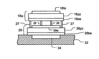
図4は、本発明の実施態様の1つに従って図3のフィルタ回路10aを設けるダイ30の平面図である。図3及び図4の場合、対応する共鳴器は、同じ参照番号で例示されている。図3の接続点は、図4では接続パッドとして例示されており、対応する接続点及び接続パッドは同じ参照番号で例示されている。図5は、ラインA−Aに沿って切断された図4のダイの一部の切り取り側面図である。ギガヘルツ周波数範囲の電子信号を濾波するフィルタ回路の場合、ダイ30の共鳴器は、それぞれ、およそ数百ミクロン以下ほどの側方サイズと、数ミクロン以下ほどの厚さを備えることが可能である。
4 is a plan view of a
図4及び図5を参照すると、ダイ30には、基板32上に製作された並列共鳴器22、24、26、及び、28が含まれている。本発明の例示の実施態様の場合、直列共鳴器12a、14a、及び、16aは、それぞれ、並列共鳴器22、24、及び、26の上方へ製作される。例えば、並列共鳴器26(第1の音響共鳴器26)は、基板32上に製作される。基板32には、第1の共鳴器26の下にキャビティ34を含むことが可能である。第2の共鳴器、この場合、直列共鳴器16aは、前記第1の共鳴器26の上方へ垂直方向に離隔されている。例示の実施態様の場合、第1の共鳴器26及び第2の共鳴器16aは、薄膜バルク音響共鳴器(FBAR)である。基板は、例えば、シリコン基板とすることが可能である。
With reference to FIGS. 4 and 5, the die 30 includes
第1の共鳴器26には、圧電層26pzを挟む下部電極26beと上部電極26teが含まれている。同様に、第2の共鳴器16aには、圧電層16pzを挟む下部電極16beと上部電極16teが含まれている。第1及び第2の共鳴器26及び16aの両方の電極は、単なる一例にすぎないが、モリブデンのような導電材料から造られている。第1及び第2の共鳴器26及び16aの両方の圧電層は、単なる一例にすぎないが、窒化アルミニウムのような圧電材料から造られている。
The
第2の共鳴器16aは、スタンドオフ(支持部材)27によって支持され、主として空気によって第1の共鳴器26から離隔され、分離されている。第1の共鳴器26と第2の共鳴器16aとの間隔は、実施例に応じて大幅に変動し、例えば、0.1ミクロン〜20ミクロンといった範囲にわたる可能性がある。実施態様によっては、セパレ−タ29によって、第1の共鳴器26と第2の共鳴器16aとの間隔を保つことが可能なものもある。図5には、2つのセパレータ29が例示されているが、セパレータ29は、垂直方向に離隔した共鳴器26及び16aが互いに接触するのを防ぐために利用されている。セパレータ29は、第1の共鳴器26の上部電極26te上に製作された短いピラーまたはスタブとすることも可能である。セパレータ29は、スタンドオフ27と同様のプロセス及び材料を用いて製作される。例示の実施態様の場合、セパレータ29の上部断面積(上部断面は図示されていない)は、第1の電極26の上部電極26teの面積(図4に部分的に例示されている)と比較して極めて小さく、例えば、上部電極26teの面積の1パーセント未満としてもよい。
The
音響共鳴器26及び16aは、垂直方向に離隔され、音響的に分離されているので、第1の音響共鳴器26と第2の音響共鳴器16aとの間で結合する音響エネルギは、ほとんどまたは全くない。
Since the
スタンドオフ27は、実施例に応じて、1ミクロンの何分のいくつかから数十ミクロンまで、あるいは、数百ミクロンにさえ及ぶ範囲のオーダで測定される高さを備えている。スタンドオフの側方長さは、0.5ミクロン〜100ミクロンの範囲とすることが可能であり、1平方ミクロン〜1平方ミリメートルにわたる断面積をなす。両共鳴器間のセパレーションは、完全であってもよく、あるいは必ずしもそうでなくてもよい。例えば、2つの共鳴器の間にスタンドオフを製作して、共鳴器を離隔することができるが、離隔した共鳴器間でスタンドオフ自体によって僅かに接続される可能性もある。
The
スタンドオフ27は、第2の共鳴器16aの下方のどこにでも製作することが可能である。例示の実施態様の場合、スタンドオフ27は、第1の共鳴器26上に製作され、第2の共鳴器16aの下部電極16beに接続されている。すなわち、例示の実施態様の場合、スタンドオフ27は、第1の共鳴器26の圧電層26pz上に製作されている。実際には、スタンドオフ27は、ダイ30の他の部分に製作することも可能である。例えば、スタンドオフ27は、基板32または第1の共鳴器26の上部電極26te上に製作することが可能である。スタンドオフ27は、例えば、タングステンのような、共鳴器製作プロセスとの統合に適した、任意の十分に合成の高い材料を用いて製作することも可能である。
The
図4のダイ30は、共鳴器を設ける領域(X軸範囲33とY軸範囲35として例示された第1と第2の寸法範囲によって形成される)を必要とする。ダイ30の共鳴器の一部は、他の共鳴器の上方へ垂直方向に離隔されている。このため、ダイ30にその共鳴器の全てを設けるのに必要な領域は、図1のダイ20に比べて少なくて済む。
The die 30 of FIG. 4 requires an area (formed by the first and second dimension ranges exemplified as the
図6は、その製作プロセス中における、ラインA−Aに沿って切断された図5のダイ30の一部に関する切り取り側面図である。その垂直方向に離隔された共鳴器を含むダイ30を製作するため、第1の共鳴器26は基板32上に製作されている。例示の実施態様の場合、第1の共鳴器26は、キャビティ34の上方に製作されている。製作プロセスのこの段階で、キャビティ34に、例えば、燐酸シリケート・ガラス(PSG)のような何らかの犠牲材料が充填される。キャビティ34のためのものとして、PSGは犠牲材料として用いられる材料と同じにすることが可能である。次に、第1の共鳴器26のまわりに、犠牲層36が製作される。第1の共鳴器26の製作後、スタンドオフ27も製作される。犠牲層36は、例えば、スラリを用いて研磨することにより、平坦化される。
6 is a cutaway side view of a portion of the
次に、第2の共鳴器16aが、スタンドオフ27の上方かつ犠牲層36の上方に製作される。最後に、犠牲層36を除去すると、スタンドオフ27によって支持され、第1の共鳴器26の上方に吊るされた第2の共鳴器16が残ることになる。PSG犠牲層の除去には、フッ化水素酸を用いることが可能である。
Next, a
図7は、本発明のもう1つの実施態様に従って共鳴器のトポロジを強調するように描き直された図1のフィルタ回路10の概略図である。この描き直されたフィルタ回路は、参照番号10bを用いて表示されている。図7のフィルタ回路10bには、図1のフィルタ回路10と同じコンポーネント共鳴器及び接続点が含まれている。さらに、図7のフィルタ回路10bの働きは、図1のフィルタ回路10の働きと同じである。このため、下記を除いては、図1及び図7の対応するコンポーネントには同じ参照番号が用いられている、すなわち、図7において、本発明の例示の実施態様に従って、垂直方向に離隔する技法をより明確に例示するため、図1の共鳴器12、14、16、24、及び、28が、図7では共鳴器12b、14b、16b、24b、及び、28bと表示されている。
FIG. 7 is a schematic diagram of the
図8は、本発明のさらなる態様を例示した、本発明の他の実施態様に従って図7のフィルタ回路10bを設けるダイ40の一部の切り取り側面図である。図7及び図8において、対応する共鳴器は、同じ参照番号で例示されている。
FIG. 8 is a cutaway side view of a portion of a die 40 that provides the
図7及び図8を参照すると、例示の実施態様において、ダイ40には、基板42上に製作された並列共鳴器22及び26が含まれている。直列共鳴器12b、14b、及び、16bが、並列共鳴器22及び26の上方へ垂直方向に離隔して製作されている。さらに、並列共鳴器24b及び28bが、直列共鳴器12b、14b、及び、16bの上方へ垂直方向に離隔して製作されている。前述のように、基板42には、共鳴器22及び26の下にキャビティ44を含むことが可能である。第2の共鳴器16bは、第1の共鳴器26の上方へ垂直方向に離隔されている。例示の実施態様の場合、第1及び第2の共鳴器26及び16bは、薄膜音響共鳴器(FBAR)である。この場合、第3の共鳴器28bが、第2の共鳴器16bの上方に製作されている。共鳴器の垂直方向へのさらなる離隔配置のため、図8のダイ40が必要とするスペースは、図4のダイ30よりもさらに少なくてすむ。
With reference to FIGS. 7 and 8, in the exemplary embodiment, die 40 includes
図8には、本発明のさらなる態様が例示されている。図8の場合、垂直方向に離隔された共鳴器を支持するためのスタンドオフは、数字41に続いて英字「a」から始まる英字が後続する参照番号(41a、41b、…)を用いて表示されている。全てのスタンドオフに対して、このように参照番号が付されているわけではない。例示の実施態様の場合、スタンドオフの1つ、すなわち、スタンドオフ41aは、基板42上に製作されているが、スタンドオフ41bのような他のスタンドオフは、下方の共鳴器の上部電極上に製作されている。実際のところ、スタンドオフ41bは、第1の共鳴器26の上部電極26teと第2の共鳴器16bの下部電極16beの間に位置し、第1の共鳴器26の上部電極26teを第2の共鳴器16bの下部電極16beに機械的に接続している。
FIG. 8 illustrates a further aspect of the present invention. In the case of FIG. 8, standoffs for supporting vertically spaced resonators are indicated using reference numbers (41a, 41b,...) Followed by a letter 41 followed by a letter starting with the letter “a”. Has been. Not all standoffs are thus given reference numbers. In the illustrated embodiment, one of the standoffs, ie,
スタンドオフ41bが、例えば、タングステンのような導電性材料で造られている場合や、電極と同じ材料であるモリブデンで造られている場合、第1の共鳴器26の上部電極26te及び第2の共鳴器16bの下部電極16beは、電気的に接続される。あるいはまた、スタンドオフ41bが電気絶縁材料で造られている場合、第1の共鳴器26の上部電極26te及び第2の共鳴器16bの下部電極16beは、電気的に互いに分離されて、互いに異なる電位を有する可能性がある。この場合、第1の共鳴器26の上部電極26teと第2の共鳴器16bの下部電極16beの間には、容量性電位差が生じる。電気的分離に関して、スタンドオフ41bは、タングステンまたはモリブデのような導電性材料、あるいは、窒化珪素またはポリシリコンのような絶縁または半絶縁材料で製作することが可能である。
When the
以上から明らかなように、本発明は、新規であって、現在の技術に対して優位性をもたらすものである。上記では、本発明の特定の実施態様について説明され、例示されているが、本発明は、こうして解説され、例示された部分の特定の形態または構成に制限されるべきものではない。例えば、異なる構成、サイズ、または、材料を利用することが可能であるが、それでも、本発明の範囲内に含まれる。本発明は、付属の請求項によって制限される。 As is apparent from the above, the present invention is novel and provides an advantage over current technology. Although specific embodiments of the present invention have been described and illustrated above, the present invention should not be limited to the specific forms or configurations of the parts so described and illustrated. For example, different configurations, sizes, or materials can be utilized, but still fall within the scope of the present invention. The invention is limited by the appended claims.
なお、本発明は例として次の態様を含む。( )内の数字は添付図面の参照符号に対応する。
[1] 基板上の第1の音響共鳴器と、
前記第1の音響共鳴器の上方にある第2の音響共鳴器が含まれている装置であって、
前記第2の音響共鳴器が、前記第1の音響共鳴器から垂直方向に離隔されていて、前記第1の音響共鳴器と前記第2の音響共鳴器との間で、音響エネルギがほとんどまたは全く結合されることのないようになっていることを特徴とする装置。
[2] 前記第1の音響共鳴器及び前記第2の音響共鳴器が薄膜バルク音響共鳴器(FBAR)であることを特徴とする、上記[1]に記載の装置。
[3] 前記第2の音響共鳴器がスタンドオフによって支持されていることを特徴とする、上記[1]に記載の装置。
[4] さらに、前記第1の音響共鳴器と前記第2の音響共鳴器の間に少なくとも1つのセパレータを備えることを特徴とする、上記[1]に記載の装置。
[5] 前記第1の音響共鳴器が、圧電層を挟む下部電極と上部電極を備え、
前記第2の音響共鳴器が、圧電層を挟む下部電極と上部電極を備えることを特徴とする、
上記[1]に記載の装置。
[6] さらに、前記第2の音響共鳴器の下部電極に接続され、前記第1音響共鳴器上に製作されるスタンドオフを備えることを特徴とする、上記[2]に記載の装置。
[7] さらに、前記第1の音響共鳴器の上部電極と前記第2の音響共鳴器の下部電極との間にスタンドオフを備えることを特徴とする、上記[5]に記載の装置。
[8] さらに、前記第1の音響共鳴器の上部電極及び前記第2の音響共鳴器の下部電極が前記スタンドオフによって電気的に接続されていることを特徴とする、上記[7]に記載の装置。
[9] 前記第1の音響共鳴器の上部電極と前記第2の音響共鳴器の下部電極が、互いに異なる電位にあり、そのため、前記第1の音響共鳴器の上部電極と前記第2の音響共鳴器の下部電極との間に容量性電位差が生じることを特徴とする、上記[7]に記載の装置。
[10] さらに、前記第1の音響共鳴器を前記第2の音響共鳴器から離隔するスタンドオフを備えることを特徴とする、上記[1]に記載の装置。
[11] 前記スタンドオフがタングステンからなることを特徴とする、上記[10]に記載の装置。
[12] 少なくとも1つのスタンドオフによって、前記第1の音響共鳴器と前記第2の音響共鳴器が電気的に接続されることを特徴とする、上記[10]に記載の装置。
[13] 前記第1の音響共鳴器が、前記第2の音響共鳴器から空気によって隔絶されていることを特徴とする、上記[1]に記載の装置。
[14] 前記第1の音響共鳴器と前記第2の音響共鳴器との間隔が、0.1ミクロン〜20ミクロンの範囲内であることを特徴とする、上記[1]に記載の装置。
[15] さらに、前記第2の音響共鳴器の上方へ垂直方向に離隔された第3の音響共鳴器を備えることを特徴とする、上記[1]に記載の装置。
[16]
基板上に製作された複数の共鳴器を具備する装置であって、
第1の音響共鳴器と、前記第1の音響共鳴器の上方で垂直方向に離隔された第2の音響共鳴器が含まれることと、
前記第2の音響共鳴器が、前記第1の音響共鳴器から音響的に分離されていることと
を特徴とする装置。
[17] 前記第2の音響共鳴器がスタンドオフによって支持されていることを特徴とする、上記[16]に記載の装置。
[18] 前記第1の音響共鳴器及び前記第2の音響共鳴器が薄膜バルク音響共鳴器(FBAR)であることを特徴とする、上記[16]に記載の装置。
[19] 前記第1の音響共鳴器が、圧電層を挟む下部電極と上部電極を備え、
前記第2の音響共鳴器が、圧電層を挟む下部電極と上部電極を備えることを特徴とする、上記[16]に記載の装置。
[20] さらに、前記第2の音響共鳴器の下部電極に接続され、前記第1の音響共鳴器の上部電極上に製作されるスタンドオフを備えることを特徴とする、上記[19]に記載の装置。
[21] さらに、前記第1の音響共鳴器の上部電極と前記第2の音響共鳴器の下部電極との間にスタンドオフを備えることを特徴とする、上記[19]に記載の装置。
[22] さらに、前記第1の音響共鳴器を前記第2の音響共鳴器から離隔するスタンドオフを備えることを特徴とする、上記[19]に記載の装置。
[23]
前記スタンドオフがタングステンからなることを特徴とする、上記[22]に記載の装置。
[24] 装置の製作方法であって、
基板上に第1の共鳴器を製作することと、
前記第1の共鳴器のまわりに犠牲層を製作することと、
スタンドオフを製作することと、
前記スタンドオフ上方において、前記犠牲層上に第2の共鳴器を製作することと、
前記犠牲層を除去することと
を有することを特徴とする方法。
[25] さらに、前記第2の共鳴器を製作する前に、前記犠牲層を平坦化することを有することを特徴とする、上記[24]に記載の方法。
In addition, this invention contains the following aspect as an example. Numbers in parentheses correspond to reference numerals in the attached drawings.
[1] a first acoustic resonator on the substrate;
A device comprising a second acoustic resonator above the first acoustic resonator, comprising:
The second acoustic resonator is vertically spaced from the first acoustic resonator, and little or no acoustic energy exists between the first acoustic resonator and the second acoustic resonator. A device characterized in that it is not coupled at all.
[2] The apparatus according to [1], wherein the first acoustic resonator and the second acoustic resonator are thin film bulk acoustic resonators (FBARs).
[3] The apparatus according to [1], wherein the second acoustic resonator is supported by a standoff.
[4] The apparatus according to [1], further comprising at least one separator between the first acoustic resonator and the second acoustic resonator.
[5] The first acoustic resonator includes a lower electrode and an upper electrode sandwiching the piezoelectric layer,
The second acoustic resonator includes a lower electrode and an upper electrode that sandwich a piezoelectric layer,
The device according to [1] above.
[6] The apparatus according to [2], further comprising a standoff connected to the lower electrode of the second acoustic resonator and manufactured on the first acoustic resonator.
[7] The apparatus according to [5], further comprising a standoff between the upper electrode of the first acoustic resonator and the lower electrode of the second acoustic resonator.
[8] The above [7], wherein the upper electrode of the first acoustic resonator and the lower electrode of the second acoustic resonator are electrically connected by the standoff. Equipment.
[9] The upper electrode of the first acoustic resonator and the lower electrode of the second acoustic resonator are at different potentials, and therefore the upper electrode of the first acoustic resonator and the second acoustic resonator The device according to [7] above, wherein a capacitive potential difference is generated between the resonator and a lower electrode of the resonator.
[10] The apparatus according to [1], further comprising a standoff that separates the first acoustic resonator from the second acoustic resonator.
[11] The apparatus according to [10], wherein the standoff is made of tungsten.
[12] The apparatus according to [10], wherein the first acoustic resonator and the second acoustic resonator are electrically connected by at least one standoff.
[13] The apparatus according to [1], wherein the first acoustic resonator is isolated from the second acoustic resonator by air.
[14] The apparatus according to [1], wherein an interval between the first acoustic resonator and the second acoustic resonator is in a range of 0.1 to 20 microns.
[15] The apparatus according to [1], further comprising a third acoustic resonator vertically spaced above the second acoustic resonator.
[16]
An apparatus comprising a plurality of resonators fabricated on a substrate,
Including a first acoustic resonator and a second acoustic resonator vertically spaced above the first acoustic resonator;
The apparatus wherein the second acoustic resonator is acoustically separated from the first acoustic resonator.
[17] The apparatus according to [16] above, wherein the second acoustic resonator is supported by a standoff.
[18] The apparatus according to [16], wherein the first acoustic resonator and the second acoustic resonator are thin film bulk acoustic resonators (FBARs).
[19] The first acoustic resonator includes a lower electrode and an upper electrode sandwiching the piezoelectric layer,
The apparatus according to [16] above, wherein the second acoustic resonator includes a lower electrode and an upper electrode that sandwich a piezoelectric layer.
[20] The above [19], further comprising a standoff connected to the lower electrode of the second acoustic resonator and manufactured on the upper electrode of the first acoustic resonator. Equipment.
[21] The device according to [19], further comprising a standoff between the upper electrode of the first acoustic resonator and the lower electrode of the second acoustic resonator.
[22] The apparatus according to [19], further comprising a standoff that separates the first acoustic resonator from the second acoustic resonator.
[23]
The apparatus according to [22] above, wherein the standoff is made of tungsten.
[24] A method of manufacturing a device,
Producing a first resonator on a substrate;
Fabricating a sacrificial layer around the first resonator;
Making standoffs,
Producing a second resonator on the sacrificial layer above the standoff;
Removing the sacrificial layer.
[25] The method according to [24] above, further comprising planarizing the sacrificial layer before fabricating the second resonator.
10 フィルタ回路
11、13、15、17、19、21 接続点(接続パッド)
12、14、16 直列共鳴器
20 ダイ
22、26、24、28 並列共鳴器
27 スタンドオフ
29 セパレータ
32 基板
10
12, 14, 16
Claims (3)
前記第1の音響共鳴器の上方にある第2の音響共鳴器と
を備えており、前記第2の音響共鳴器が、前記第1の音響共鳴器から垂直方向に離隔されていて、前記第1の音響共鳴器と前記第2の音響共鳴器との間で、音響エネルギがほとんどまたは全く結合されることのないようになっており、
前記第1の音響共鳴器を前記第2の音響共鳴器から離隔するスタンドオフを備えており、該スタンドオフはタングステンを含んでおり、
前記第1の音響共鳴器と前記第2の音響共鳴器との間隔が0.1ミクロンから20ミクロンの範囲内にある、装置。 A first acoustic resonator on the substrate;
A second acoustic resonator above the first acoustic resonator, wherein the second acoustic resonator is vertically spaced from the first acoustic resonator, and Little or no acoustic energy is coupled between one acoustic resonator and the second acoustic resonator;
A standoff that separates the first acoustic resonator from the second acoustic resonator, the standoff comprising tungsten;
The apparatus wherein the distance between the first acoustic resonator and the second acoustic resonator is in the range of 0.1 microns to 20 microns.
前記複数の共鳴器は、第1の音響共鳴器と、該第1の音響共鳴器から垂直方向に離隔されている第2の音響共鳴器とを含んでおり、
前記第2の音響共鳴器は、前記第1の音響共鳴器とは音響的に分離されており、
前記第1の音響共鳴器が下部電極と上部電極とを備えており、該下部電極と該上部電極との間には圧電層が設けられており、
前記第2の音響共鳴器が下部電極と上部電極とを備えており、該下部電極と該上部電極との間には圧電層が設けられており、
前記第1の音響共鳴器の上部電極にはスタンドオフが設けられており、前記第1の音響共鳴器の上部電極と前記第2の音響共鳴器の下部電極とが前記スタンドオフにより電気的に接続しており、
前記第1の音響共鳴器と前記第2の音響共鳴器との間隔が0.1ミクロンから20ミクロンの範囲内にある、装置。 A plurality of resonators provided on a substrate;
The plurality of resonators include a first acoustic resonator and a second acoustic resonator that is vertically spaced from the first acoustic resonator;
The second acoustic resonator is acoustically separated from the first acoustic resonator;
The first acoustic resonator includes a lower electrode and an upper electrode, and a piezoelectric layer is provided between the lower electrode and the upper electrode,
The second acoustic resonator includes a lower electrode and an upper electrode, and a piezoelectric layer is provided between the lower electrode and the upper electrode,
The upper electrode of the first acoustic resonator is provided with a standoff, and the upper electrode of the first acoustic resonator and the lower electrode of the second acoustic resonator are electrically connected by the standoff. Connected
The apparatus wherein the distance between the first acoustic resonator and the second acoustic resonator is in the range of 0.1 microns to 20 microns.
前記複数の共鳴器は、第1の音響共鳴器と、該第1の音響共鳴器から垂直方向に離隔されている第2の音響共鳴器とを含んでおり、
前記第2の音響共鳴器は、前記第1の音響共鳴器とは音響的に分離されており、
前記第1の音響共鳴器が下部電極と上部電極とを備えており、該下部電極と該上部電極との間には圧電層が設けられており、
前記第2の音響共鳴器が下部電極と上部電極とを備えており、該下部電極と該上部電極との間には圧電層が設けられており、
前記第1の音響共鳴器と前記第2の音響共鳴器とを離隔するスタンドオフが設けられており、該スタンドオフはタングステンを含んでおり、
前記第1の音響共鳴器と前記第2の音響共鳴器との間隔が0.1ミクロンから20ミクロンの範囲内にある、装置。 A plurality of resonators provided on a substrate;
The plurality of resonators include a first acoustic resonator and a second acoustic resonator that is vertically spaced from the first acoustic resonator;
The second acoustic resonator is acoustically separated from the first acoustic resonator;
The first acoustic resonator includes a lower electrode and an upper electrode, and a piezoelectric layer is provided between the lower electrode and the upper electrode,
The second acoustic resonator includes a lower electrode and an upper electrode, and a piezoelectric layer is provided between the lower electrode and the upper electrode,
A standoff is provided to separate the first acoustic resonator and the second acoustic resonator, the standoff comprising tungsten;
The apparatus wherein the distance between the first acoustic resonator and the second acoustic resonator is in the range of 0.1 microns to 20 microns.
Applications Claiming Priority (1)
| Application Number | Priority Date | Filing Date | Title |
|---|---|---|---|
| US10/785,525 US7038559B2 (en) | 2004-02-23 | 2004-02-23 | Vertically separated acoustic filters and resonators |
Publications (3)
| Publication Number | Publication Date |
|---|---|
| JP2005244966A JP2005244966A (en) | 2005-09-08 |
| JP2005244966A5 JP2005244966A5 (en) | 2007-07-12 |
| JP4683947B2 true JP4683947B2 (en) | 2011-05-18 |
Family
ID=34274940
Family Applications (1)
| Application Number | Title | Priority Date | Filing Date |
|---|---|---|---|
| JP2005035841A Expired - Fee Related JP4683947B2 (en) | 2004-02-23 | 2005-02-14 | Vertically separated acoustic filter and resonator |
Country Status (3)
| Country | Link |
|---|---|
| US (5) | US7038559B2 (en) |
| JP (1) | JP4683947B2 (en) |
| GB (1) | GB2411302B (en) |
Families Citing this family (34)
| Publication number | Priority date | Publication date | Assignee | Title |
|---|---|---|---|---|
| US7627552B2 (en) | 2003-03-27 | 2009-12-01 | Microsoft Corporation | System and method for filtering and organizing items based on common elements |
| KR100485702B1 (en) * | 2003-05-29 | 2005-04-28 | 삼성전자주식회사 | Film bulk acoustic resonator having support structure and method thereof |
| US7038559B2 (en) * | 2004-02-23 | 2006-05-02 | Ruby Richard C | Vertically separated acoustic filters and resonators |
| JP2006060385A (en) * | 2004-08-18 | 2006-03-02 | Matsushita Electric Ind Co Ltd | Resonator and filter using the same |
| US7248131B2 (en) * | 2005-03-14 | 2007-07-24 | Avago Technologies Wireless Ip (Singapore) Pte. Ltd. | Monolithic vertical integration of an acoustic resonator and electronic circuitry |
| US7665028B2 (en) | 2005-07-13 | 2010-02-16 | Microsoft Corporation | Rich drag drop user interface |
| US7623007B2 (en) * | 2005-10-19 | 2009-11-24 | Panasonic Corporation | Device including piezoelectric thin film and a support having a vertical cross-section with a curvature |
| US20070093229A1 (en) * | 2005-10-20 | 2007-04-26 | Takehiko Yamakawa | Complex RF device and method for manufacturing the same |
| US7561009B2 (en) * | 2005-11-30 | 2009-07-14 | Avago Technologies General Ip (Singapore) Pte. Ltd. | Film bulk acoustic resonator (FBAR) devices with temperature compensation |
| JP2008172711A (en) | 2007-01-15 | 2008-07-24 | Hitachi Media Electoronics Co Ltd | Thin film bulk acoustic wave resonator, filter, and high frequency module using it |
| JP5226409B2 (en) * | 2008-07-17 | 2013-07-03 | 太陽誘電株式会社 | RESONANT DEVICE, COMMUNICATION MODULE, COMMUNICATION DEVICE, AND RESONANT DEVICE MANUFACTURING METHOD |
| US9520856B2 (en) | 2009-06-24 | 2016-12-13 | Avago Technologies General Ip (Singapore) Pte. Ltd. | Acoustic resonator structure having an electrode with a cantilevered portion |
| WO2011153246A2 (en) | 2010-06-01 | 2011-12-08 | Martek Biosciences Corporation | Extraction of lipid from cells and products therefrom |
| US9425764B2 (en) | 2012-10-25 | 2016-08-23 | Avago Technologies General Ip (Singapore) Pte. Ltd. | Accoustic resonator having composite electrodes with integrated lateral features |
| US9203374B2 (en) | 2011-02-28 | 2015-12-01 | Avago Technologies General Ip (Singapore) Pte. Ltd. | Film bulk acoustic resonator comprising a bridge |
| US9099983B2 (en) | 2011-02-28 | 2015-08-04 | Avago Technologies General Ip (Singapore) Pte. Ltd. | Bulk acoustic wave resonator device comprising a bridge in an acoustic reflector |
| US9444426B2 (en) | 2012-10-25 | 2016-09-13 | Avago Technologies General Ip (Singapore) Pte. Ltd. | Accoustic resonator having integrated lateral feature and temperature compensation feature |
| US8922302B2 (en) | 2011-08-24 | 2014-12-30 | Avago Technologies General Ip (Singapore) Pte. Ltd. | Acoustic resonator formed on a pedestal |
| US9667218B2 (en) | 2012-01-30 | 2017-05-30 | Avago Technologies General Ip (Singapore) Pte. Ltd. | Temperature controlled acoustic resonator comprising feedback circuit |
| US9608592B2 (en) | 2014-01-21 | 2017-03-28 | Avago Technologies General Ip (Singapore) Pte. Ltd. | Film bulk acoustic wave resonator (FBAR) having stress-relief |
| US9667220B2 (en) | 2012-01-30 | 2017-05-30 | Avago Technologies General Ip (Singapore) Pte. Ltd. | Temperature controlled acoustic resonator comprising heater and sense resistors |
| US9154103B2 (en) | 2012-01-30 | 2015-10-06 | Avago Technologies General Ip (Singapore) Pte. Ltd. | Temperature controlled acoustic resonator |
| DE102013102206B4 (en) | 2013-03-06 | 2016-04-07 | Epcos Ag | Device with stacked functional structures and method of manufacture |
| US10342772B2 (en) | 2013-12-20 | 2019-07-09 | Dsm Ip Assets B.V. | Processes for obtaining microbial oil from microbial cells |
| EP3082792A4 (en) | 2013-12-20 | 2017-08-16 | DSM IP Assets B.V. | Processes for obtaining microbial oil from microbial cells |
| TWI646188B (en) | 2013-12-20 | 2019-01-01 | 荷蘭商Dsm智慧財產有限公司 | Method for obtaining microbial oil from microbial cells (4) |
| CN106061475B (en) | 2013-12-20 | 2022-03-25 | 帝斯曼知识产权资产管理有限公司 | Method for obtaining microbial oil from microbial cells |
| JP6454299B2 (en) * | 2016-05-13 | 2019-01-16 | 太陽誘電株式会社 | Elastic wave device |
| US11616488B2 (en) * | 2016-09-30 | 2023-03-28 | Intel Corporation | FBAR devices having multiple epitaxial layers stacked on a same substrate |
| US10804880B2 (en) * | 2018-12-03 | 2020-10-13 | X-Celeprint Limited | Device structures with acoustic wave transducers and connection posts |
| US11274035B2 (en) | 2019-04-24 | 2022-03-15 | X-Celeprint Limited | Overhanging device structures and related methods of manufacture |
| US20210002128A1 (en) | 2018-12-03 | 2021-01-07 | X-Celeprint Limited | Enclosed cavity structures |
| US20230155570A1 (en) * | 2020-04-20 | 2023-05-18 | Suzhou Huntersun Electronics Co., Ltd. | Bulk acoustic wave resonator and fabrication method therefor |
| CN112187212B (en) * | 2020-09-18 | 2021-12-07 | 杭州星阖科技有限公司 | Acoustic resonator assembly and filter |
Citations (8)
| Publication number | Priority date | Publication date | Assignee | Title |
|---|---|---|---|---|
| US5185589A (en) * | 1991-05-17 | 1993-02-09 | Westinghouse Electric Corp. | Microwave film bulk acoustic resonator and manifolded filter bank |
| JPH09270669A (en) * | 1996-04-01 | 1997-10-14 | Murata Mfg Co Ltd | Ladder form filter |
| JPH11346140A (en) * | 1998-04-08 | 1999-12-14 | Nokia Mobile Phones Ltd | Monolithic filter using thin film bulk elastic wave device and minimum passive element for controlling shape and width of passband response |
| WO2002039537A1 (en) * | 2000-11-13 | 2002-05-16 | Mems Solution Inc. | Thin film resonator and method for manufacturing the same |
| JP2003017964A (en) * | 2001-07-04 | 2003-01-17 | Hitachi Ltd | Manufacturing method for acoustic wave element |
| US6635519B2 (en) * | 2002-01-10 | 2003-10-21 | Agere Systems, Inc. | Structurally supported thin film resonator and method of fabrication |
| JP2004357306A (en) * | 2003-05-29 | 2004-12-16 | Samsung Electronics Co Ltd | Thin-film bulk acoustic resonator with support, and manufacturing method therefor |
| US7038559B2 (en) * | 2004-02-23 | 2006-05-02 | Ruby Richard C | Vertically separated acoustic filters and resonators |
Family Cites Families (20)
| Publication number | Priority date | Publication date | Assignee | Title |
|---|---|---|---|---|
| US3422371A (en) * | 1967-07-24 | 1969-01-14 | Sanders Associates Inc | Thin film piezoelectric oscillator |
| US4058745A (en) * | 1976-07-06 | 1977-11-15 | Hughes Aircraft Company | Controlled gap surface acoustic wave device |
| US5587620A (en) | 1993-12-21 | 1996-12-24 | Hewlett-Packard Company | Tunable thin film acoustic resonators and method for making the same |
| US5864261A (en) * | 1994-05-23 | 1999-01-26 | Iowa State University Research Foundation | Multiple layer acoustical structures for thin-film resonator based circuits and systems |
| US6060818A (en) | 1998-06-02 | 2000-05-09 | Hewlett-Packard Company | SBAR structures and method of fabrication of SBAR.FBAR film processing techniques for the manufacturing of SBAR/BAR filters |
| US6228675B1 (en) | 1999-07-23 | 2001-05-08 | Agilent Technologies, Inc. | Microcap wafer-level package with vias |
| US6265246B1 (en) | 1999-07-23 | 2001-07-24 | Agilent Technologies, Inc. | Microcap wafer-level package |
| JP4420538B2 (en) | 1999-07-23 | 2010-02-24 | アバゴ・テクノロジーズ・ワイヤレス・アイピー(シンガポール)プライベート・リミテッド | Wafer package manufacturing method |
| US6466107B2 (en) * | 1999-12-14 | 2002-10-15 | Murata Manufacturing Co., Ltd. | Ladder filter comprising stacked piezoelectric resonators |
| US7296329B1 (en) | 2000-02-04 | 2007-11-20 | Agere Systems Inc. | Method of isolation for acoustic resonator device |
| US6384697B1 (en) | 2000-05-08 | 2002-05-07 | Agilent Technologies, Inc. | Cavity spanning bottom electrode of a substrate-mounted bulk wave acoustic resonator |
| US6486751B1 (en) | 2000-09-26 | 2002-11-26 | Agere Systems Inc. | Increased bandwidth thin film resonator having a columnar structure |
| WO2002058233A1 (en) * | 2001-01-18 | 2002-07-25 | Infineon Technologies Ag | Filter devices and method for fabricating filter devices |
| TW488044B (en) * | 2001-02-09 | 2002-05-21 | Asia Pacific Microsystems Inc | Bulk acoustic filter and its package |
| US6720844B1 (en) * | 2001-11-16 | 2004-04-13 | Tfr Technologies, Inc. | Coupled resonator bulk acoustic wave filter |
| US6670866B2 (en) * | 2002-01-09 | 2003-12-30 | Nokia Corporation | Bulk acoustic wave resonator with two piezoelectric layers as balun in filters and duplexers |
| US6811312B2 (en) | 2002-02-08 | 2004-11-02 | Schick Technologies, Inc. | Dental x-ray positioning using adhesives |
| DE10256937B4 (en) * | 2002-12-05 | 2018-02-01 | Snaptrack, Inc. | With bulk acoustic waves working device with unbalanced / balanced wiring |
| KR100486627B1 (en) * | 2003-02-21 | 2005-05-03 | 엘지전자 주식회사 | Semiconductor package |
| US7400217B2 (en) * | 2003-10-30 | 2008-07-15 | Avago Technologies Wireless Ip Pte Ltd | Decoupled stacked bulk acoustic resonator band-pass filter with controllable pass bandwith |
-
2004
- 2004-02-23 US US10/785,525 patent/US7038559B2/en not_active Expired - Fee Related
-
2005
- 2005-01-21 GB GB0501315A patent/GB2411302B/en not_active Expired - Fee Related
- 2005-02-14 JP JP2005035841A patent/JP4683947B2/en not_active Expired - Fee Related
- 2005-08-11 US US11/203,003 patent/US7563475B2/en not_active Expired - Fee Related
-
2006
- 2006-03-09 US US11/373,355 patent/US7312675B2/en not_active Expired - Fee Related
- 2006-03-09 US US11/373,451 patent/US7841055B2/en not_active Expired - Fee Related
-
2010
- 2010-11-09 US US12/942,375 patent/US20110047783A1/en not_active Abandoned
Patent Citations (9)
| Publication number | Priority date | Publication date | Assignee | Title |
|---|---|---|---|---|
| US5185589A (en) * | 1991-05-17 | 1993-02-09 | Westinghouse Electric Corp. | Microwave film bulk acoustic resonator and manifolded filter bank |
| JPH09270669A (en) * | 1996-04-01 | 1997-10-14 | Murata Mfg Co Ltd | Ladder form filter |
| JPH11346140A (en) * | 1998-04-08 | 1999-12-14 | Nokia Mobile Phones Ltd | Monolithic filter using thin film bulk elastic wave device and minimum passive element for controlling shape and width of passband response |
| WO2002039537A1 (en) * | 2000-11-13 | 2002-05-16 | Mems Solution Inc. | Thin film resonator and method for manufacturing the same |
| JP2004514313A (en) * | 2000-11-13 | 2004-05-13 | メムズ ソリューション インコーポレイテッド | Thin film resonator and manufacturing method thereof |
| JP2003017964A (en) * | 2001-07-04 | 2003-01-17 | Hitachi Ltd | Manufacturing method for acoustic wave element |
| US6635519B2 (en) * | 2002-01-10 | 2003-10-21 | Agere Systems, Inc. | Structurally supported thin film resonator and method of fabrication |
| JP2004357306A (en) * | 2003-05-29 | 2004-12-16 | Samsung Electronics Co Ltd | Thin-film bulk acoustic resonator with support, and manufacturing method therefor |
| US7038559B2 (en) * | 2004-02-23 | 2006-05-02 | Ruby Richard C | Vertically separated acoustic filters and resonators |
Also Published As
| Publication number | Publication date |
|---|---|
| US20050184830A1 (en) | 2005-08-25 |
| US7841055B2 (en) | 2010-11-30 |
| US7038559B2 (en) | 2006-05-02 |
| GB0501315D0 (en) | 2005-03-02 |
| US20060152305A1 (en) | 2006-07-13 |
| US20110047783A1 (en) | 2011-03-03 |
| GB2411302B (en) | 2007-04-18 |
| US7563475B2 (en) | 2009-07-21 |
| US20060016070A1 (en) | 2006-01-26 |
| JP2005244966A (en) | 2005-09-08 |
| US7312675B2 (en) | 2007-12-25 |
| US20060158284A1 (en) | 2006-07-20 |
| GB2411302A (en) | 2005-08-24 |
Similar Documents
| Publication | Publication Date | Title |
|---|---|---|
| JP4683947B2 (en) | Vertically separated acoustic filter and resonator | |
| EP1482638B1 (en) | Film bulk acoustic resonator having supports and manufacturing method therefor | |
| JP4189637B2 (en) | FILTER, COMPOSITE FILTER, FILTER MOUNTING BODY WITH THE SAME, INTEGRATED CIRCUIT CHIP, ELECTRONIC DEVICE, AND METHOD FOR CHANGE THE FREQUENCY CHARACTERISTICS OF THE SAME | |
| US7023065B2 (en) | Capacitive resonators and methods of fabrication | |
| CN103684336B (en) | Resonator device with electrode comprising embedded type temperature compensation layer | |
| US8482357B2 (en) | Transverse acoustic wave resonator, oscillator having the resonator and method for making the resonator | |
| KR20160086552A (en) | Acoustic resonator and manufacturing method thereof | |
| CN101931380A (en) | The acoustic resonator structure that comprises bridge portion | |
| JP2005533400A (en) | Micro-bridge structure with reduced central mass for very high frequency MEM resonators | |
| CN111146328A (en) | Single crystal piezoelectric structure and electronic device having the same | |
| CN111313859B (en) | Bulk acoustic wave resonator, method of manufacturing the same, filter, and electronic apparatus | |
| JP2008079294A (en) | Thin film bulk elastic wave resonator and method for manufacturing same | |
| CN113824419A (en) | Method for forming piezoelectric film and method for forming bulk acoustic wave resonator | |
| US6563400B2 (en) | Piezoelectric resonator utilizing bending vibrations and ladder-type filter including the same | |
| EP1568655B1 (en) | Micromachine and method of producing the same | |
| KR20010040089A (en) | Piezoelectric resonator | |
| JP4254445B2 (en) | Microelectromechanical system resonator and driving method thereof | |
| JP4389518B2 (en) | Micro-electromechanical system resonator and method for adjusting the same | |
| KR100518828B1 (en) | MEMS structure for metal interconnection and fabrication method thereof | |
| US20240137004A1 (en) | Acoustic resonator lid for thermal transport | |
| JP4155209B2 (en) | Microelectromechanical system resonator, manufacturing method thereof, and frequency filter | |
| CN117915250A (en) | Acoustic resonator cover for heat transfer | |
| US8760234B2 (en) | MEMS vibrator and oscillator | |
| CN116073782A (en) | Hybrid filter | |
| CN116526997A (en) | Film bulk acoustic resonator and manufacturing method thereof |
Legal Events
| Date | Code | Title | Description |
|---|---|---|---|
| A711 | Notification of change in applicant |
Free format text: JAPANESE INTERMEDIATE CODE: A711 Effective date: 20070328 |
|
| RD03 | Notification of appointment of power of attorney |
Free format text: JAPANESE INTERMEDIATE CODE: A7423 Effective date: 20070409 |
|
| A521 | Request for written amendment filed |
Free format text: JAPANESE INTERMEDIATE CODE: A523 Effective date: 20070525 |
|
| A621 | Written request for application examination |
Free format text: JAPANESE INTERMEDIATE CODE: A621 Effective date: 20070525 |
|
| RD03 | Notification of appointment of power of attorney |
Free format text: JAPANESE INTERMEDIATE CODE: A7423 Effective date: 20071206 |
|
| RD04 | Notification of resignation of power of attorney |
Free format text: JAPANESE INTERMEDIATE CODE: A7424 Effective date: 20071220 |
|
| A977 | Report on retrieval |
Free format text: JAPANESE INTERMEDIATE CODE: A971007 Effective date: 20100430 |
|
| A131 | Notification of reasons for refusal |
Free format text: JAPANESE INTERMEDIATE CODE: A131 Effective date: 20100514 |
|
| A521 | Request for written amendment filed |
Free format text: JAPANESE INTERMEDIATE CODE: A523 Effective date: 20100727 |
|
| A131 | Notification of reasons for refusal |
Free format text: JAPANESE INTERMEDIATE CODE: A131 Effective date: 20100922 |
|
| A521 | Request for written amendment filed |
Free format text: JAPANESE INTERMEDIATE CODE: A523 Effective date: 20101206 |
|
| TRDD | Decision of grant or rejection written | ||
| A01 | Written decision to grant a patent or to grant a registration (utility model) |
Free format text: JAPANESE INTERMEDIATE CODE: A01 Effective date: 20110204 |
|
| A01 | Written decision to grant a patent or to grant a registration (utility model) |
Free format text: JAPANESE INTERMEDIATE CODE: A01 |
|
| A61 | First payment of annual fees (during grant procedure) |
Free format text: JAPANESE INTERMEDIATE CODE: A61 Effective date: 20110208 |
|
| FPAY | Renewal fee payment (event date is renewal date of database) |
Free format text: PAYMENT UNTIL: 20140218 Year of fee payment: 3 |
|
| R150 | Certificate of patent or registration of utility model |
Free format text: JAPANESE INTERMEDIATE CODE: R150 |
|
| FPAY | Renewal fee payment (event date is renewal date of database) |
Free format text: PAYMENT UNTIL: 20140218 Year of fee payment: 3 |
|
| RD02 | Notification of acceptance of power of attorney |
Free format text: JAPANESE INTERMEDIATE CODE: R3D02 |
|
| FPAY | Renewal fee payment (event date is renewal date of database) |
Free format text: PAYMENT UNTIL: 20140218 Year of fee payment: 3 |
|
| RD02 | Notification of acceptance of power of attorney |
Free format text: JAPANESE INTERMEDIATE CODE: R3D02 |
|
| S111 | Request for change of ownership or part of ownership |
Free format text: JAPANESE INTERMEDIATE CODE: R313111 |
|
| R360 | Written notification for declining of transfer of rights |
Free format text: JAPANESE INTERMEDIATE CODE: R360 |
|
| R370 | Written measure of declining of transfer procedure |
Free format text: JAPANESE INTERMEDIATE CODE: R370 |
|
| LAPS | Cancellation because of no payment of annual fees |