JP4155209B2 - Microelectromechanical system resonator, manufacturing method thereof, and frequency filter - Google Patents
Microelectromechanical system resonator, manufacturing method thereof, and frequency filter Download PDFInfo
- Publication number
- JP4155209B2 JP4155209B2 JP2004049133A JP2004049133A JP4155209B2 JP 4155209 B2 JP4155209 B2 JP 4155209B2 JP 2004049133 A JP2004049133 A JP 2004049133A JP 2004049133 A JP2004049133 A JP 2004049133A JP 4155209 B2 JP4155209 B2 JP 4155209B2
- Authority
- JP
- Japan
- Prior art keywords
- electrode
- input
- output
- vibrator
- input electrode
- Prior art date
- Legal status (The legal status is an assumption and is not a legal conclusion. Google has not performed a legal analysis and makes no representation as to the accuracy of the status listed.)
- Expired - Fee Related
Links
Images


Description
本発明は、平衡入力により平衡出力が容易なマイクロ電気機械システムの共振器およびその製造方法および周波数フィルタに関するものである。 The present invention relates to a resonator of a microelectromechanical system that easily achieves a balanced output by a balanced input, a manufacturing method thereof, and a frequency filter.
情報通信技術の発展に伴って、近年ネットワークを利用するデバイスの数は飛躍的に増加しており、使い勝手の面からも、無線ネットワーク技術に対する需要が高まっている。 With the development of information communication technology, the number of devices that use a network has increased dramatically in recent years, and the demand for wireless network technology is increasing from the viewpoint of usability.
無線通信で用いられるRF(ラジオ周波)フロントエンドモジュールには、半導体チップのほかに、RFフィルタ、IF(中間周波)フィルタ用に表面弾性波(SAW)フィルタや誘電体フィルタなど、比較的サイズの大きな部品が存在しており、これらの存在がRFフロントエンドの小型化と低コスト化を阻んできた。これらのフィルタ機能を半導体チップの中に取り込むことが現在求められている。 RF (radio frequency) front-end modules used in wireless communications include relatively small sizes such as surface acoustic wave (SAW) filters and dielectric filters for RF filters and IF (intermediate frequency) filters in addition to semiconductor chips. There are large parts, and these existences have prevented the RF front end from being reduced in size and cost. It is currently required to incorporate these filter functions into a semiconductor chip.
半導体プロセス技術を用いて形成された微小振動子は、デバイスの占有面積が小さいこと、高いQ値を実現できること、他の半導体デバイスとの集積が可能であること等の特徴により、無線通信デバイスの中でもIFフィルタ、RFフィルタとしての利用がミシガン大学を始めとする研究機関から提案されている(例えば、非特許文献1参照)。 A micro vibrator formed by using a semiconductor process technology has features such as a small area occupied by the device, a high Q value, and the ability to integrate with other semiconductor devices. Among them, the use as an IF filter and an RF filter has been proposed by research institutions such as the University of Michigan (see, for example, Non-Patent Document 1).
しかし、これまでに提案され、検証された微小振動子の共振周波数は最高でも200MHzを超えず、従来の表面弾性波(SAW)あるいは薄膜弾性波(FBAR)によるGHz(ギガヘルツ)領域のフィルタに対して、微小振動子の特性である高いQ値をGHz帯周波数領域で提供することは困難となっている。 However, the resonance frequency of the micro-vibrator that has been proposed and verified so far does not exceed 200 MHz at the maximum. Thus, it is difficult to provide a high Q value, which is a characteristic of the micro vibrator, in the GHz band frequency region.
現在のところ、一般に高い周波数領域では出力信号としての共振ピークが小さくなる傾向があり、良好なフィルタ特性を得るためには、共振ピークのSN比を向上する必要がある。ミシガン大学の文献(Disk型の例)(例えば、非特許文献1参照)によれば、出力信号のノイズ成分は、入出力電極間に構成される寄生容量を直接透過する信号によっており、この信号を小さくするために、直流(DC)を印加した振動電極を入出力電極間に配置することで、ノイズ成分の低減が図れるとされている。 At present, the resonance peak as an output signal generally tends to be small in a high frequency region, and it is necessary to improve the SN ratio of the resonance peak in order to obtain good filter characteristics. According to the University of Michigan literature (Example of Disk type) (see, for example, Non-Patent Document 1), the noise component of the output signal depends on a signal that directly passes through the parasitic capacitance formed between the input and output electrodes. In order to reduce the noise, a vibration component to which direct current (DC) is applied is arranged between the input and output electrodes, thereby reducing noise components.
一方でDisk型の振動子で、十分な出力信号を得るには、30Vを超えるDC電圧が必要であるために、実用的な構造としては両持ち梁を用いたビーム型の構造が望ましい。上記のノイズ成分の低減方法をビーム型の構造に対して適用した場合、一例として図9に示すような電極配置となる。 On the other hand, in order to obtain a sufficient output signal with a disk-type vibrator, a DC voltage exceeding 30 V is required. Therefore, a beam-type structure using a doubly supported beam is desirable as a practical structure. When the above noise component reduction method is applied to a beam-type structure, an electrode arrangement as shown in FIG. 9 is taken as an example.
図9に示すように、シリコン基板上に酸化シリコン膜および窒化シリコン膜の積層膜を形成した基板310上に、離間した状態で入力電極311と出力電極312とが平行に配設され、その上空に微小な空間321を介して上記入力電極311および上記出力電極312を横切るようにビーム型振動子313が配設されているものである。また、図面に示した曲線はビーム型振動子313の振動曲線を示す。
As shown in FIG. 9, an
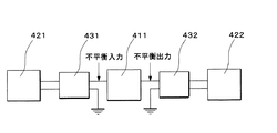
このような共振器では、振動子313は2次モードの振動となり、不平衡入力で不平衡出力となる。このような共振器を平衡入力の周波数フィルタに用いた場合、図10に示すように、前段デバイス(例えば集積回路)421からの出力信号(平衡入力)を、周波数フィルタ411にとって不平衡入力とするためのバラン素子431と、周波数フィルタ411の出力段に周波数フィルタ411からの不平衡出力を平衡出力とするためのバラン素子432を接続する必要がある。これによって、周波数フィルタ411に接続されている後段デバイス(例えば集積回路)422に平衡入力信号が入力できるようになる。
In such a resonator, the
解決しようとする問題点は、従来のマイクロ電気機械システムの共振器は、不平衡入力し、不平衡出力するデバイスである点である。現在の通信機器では、集積回路内は平衡信号が主流となっており、従来のMEMS共振器を使うためには、例えばIFフィルタなどへの応用のためには、不平衡平衡変換器(Balun)が必要である点である。これはコストの増加と、サイズの増加を意味し、MEMS共振器の採用を困難にしていた。 The problem to be solved is that the resonator of the conventional microelectromechanical system is a device that inputs an unbalance and outputs an unbalance. In current communication equipment, a balanced signal is mainly used in an integrated circuit. In order to use a conventional MEMS resonator, for example, an application to an IF filter, an unbalanced balanced converter (Barun) is used. Is a necessary point. This means an increase in cost and an increase in size, making it difficult to employ a MEMS resonator.
本発明のマイクロ電気機械システムの共振器は、信号を入力する入力電極と、信号を出力する出力電極と、前記入力電極および前記出力電極に対して空間を介して対向する振動子とを備えたマイクロ電気機械システムの共振器において、前記入力電極に平衡で信号が入力され、前記出力電極は平衡で信号が出力され、前記入力電極は第1入力電極と第2入力電極とからなり、前記出力電極は第1出力電極と第2出力電極とからなり、前記第1入力電極と前記第1出力電極とはそれぞれの位置における前記振動子の振幅の位相が同位相となるように配置され、第2入力電極と第2出力電極とはそれぞれの位置における前記振動子の振幅の位相が同位相の位置でかつ前記第1入力電極の位置における前記振動子の振幅の位相とは180度異なる位相となるように配置されていることを最も主要な特徴とする。 A resonator of a micro electro mechanical system of the present invention includes an input electrode for inputting a signal, an output electrode for outputting a signal, and a vibrator facing the input electrode and the output electrode through a space. In the resonator of the micro electro mechanical system, a signal is input to the input electrode in a balanced manner, the output electrode is output in a balanced manner , the input electrode includes a first input electrode and a second input electrode, and the output The electrode includes a first output electrode and a second output electrode, and the first input electrode and the first output electrode are arranged such that the phase of the amplitude of the vibrator at each position is the same, The two input electrodes and the second output electrode have a position where the amplitude of the vibrator at the respective positions is in the same phase and are 180 degrees different from the amplitude of the vibrator at the position of the first input electrode. The most important features that they are being arranged such that.
本発明のマイクロ電気機械システムの共振器の製造方法は、信号を入力する入力電極と、信号を出力する出力電極と、前記入力電極および前記出力電極に対して空間を介して対向する振動子とを備えたマイクロ電気機械システムの共振器の製造方法において、前記入力電極と前記出力電極とは同時に形成され、前記入力電極には第1入力電極と第2入力電極とを形成し、前記出力電極には第1出力電極と第2出力電極とを形成し、前記第1入力電極と前記第1出力電極とはそれぞれの位置における前記振動子の振幅の位相が同位相となるように配置され、第2入力電極と第2出力電極とはそれぞれの位置における前記振動子の振幅の位相が同位相となるようにかつ前記第1入力電極の位置における前記振動子の振幅の位相とは180度異なる位相となるように配置されることを最も主要な特徴とする。 A method of manufacturing a resonator of a micro electro mechanical system of the present invention includes an input electrode for inputting a signal, an output electrode for outputting a signal, and a vibrator facing the input electrode and the output electrode through a space. The input electrode and the output electrode are formed at the same time, and the input electrode is formed with a first input electrode and a second input electrode, and the output electrode Forming a first output electrode and a second output electrode, wherein the first input electrode and the first output electrode are arranged so that the phase of the amplitude of the vibrator at each position is the same phase, The second input electrode and the second output electrode are 180 degrees different from each other so that the phase of the amplitude of the vibrator at the respective positions is the same and the phase of the amplitude of the vibrator at the position of the first input electrode. The most important being arranged such that the phases.
本発明の周波数フィルタは、信号を入力する入力電極と、信号を出力する出力電極と、前記入力電極および前記出力電極に対して空間を介して対向する振動子とを備えたマイクロ電気機械システムの共振器を備えた周波数フィルタにおいて、前記入力電極に平衡で信号が入力され、前記出力電極は平衡で信号が出力され、前記入力電極は第1入力電極と第2入力電極とからなり、前記出力電極は第1出力電極と第2出力電極とからなり、前記第1入力電極と前記第1出力電極とはそれぞれの位置における前記振動子の振幅の位相が同位相となるように配置され、第2入力電極と第2出力電極とはそれぞれの位置における前記振動子の振幅の位相が同位相の位置でかつ前記第1入力電極の位置における前記振動子の振幅の位相とは180度異なる位相となるように配置されていることを最も主要な特徴とする。 The frequency filter of the present invention is a micro electro mechanical system including an input electrode for inputting a signal, an output electrode for outputting a signal, and a vibrator facing the input electrode and the output electrode through a space. In a frequency filter including a resonator, a signal is input to the input electrode in a balanced manner, the output electrode is output in a balanced manner , the input electrode includes a first input electrode and a second input electrode, and the output The electrode includes a first output electrode and a second output electrode, and the first input electrode and the first output electrode are arranged such that the phase of the amplitude of the vibrator at each position is the same, The two input electrodes and the second output electrode are in the same phase of the amplitude of the vibrator at the respective positions, and are 180 degrees different from the amplitude of the vibrator at the position of the first input electrode. The most important features that you have been arranged so that phase.
本発明のマイクロ電気機械システムの共振器(以下MEMS共振器と記す)は、平衡で入力する入力電極と平衡で出力する出力電極とを備えていることから、平衡入力、平衡出力が可能になる。このため、本発明のMEMS共振器を用いている周波数フィルタ、特にRFフィルタやIFフィルタにおいては、従来のビーム式共振器を用いたRFフィルタやIFフィルタで必要であったバラン素子が必要なくなり、回路の単純化、小型化、低コスト化が可能となるという利点がある。 Since the resonator of the micro electro mechanical system of the present invention (hereinafter referred to as a MEMS resonator) includes an input electrode that is input in a balanced manner and an output electrode that is output in a balanced manner, balanced input and balanced output are possible. . For this reason, in the frequency filter using the MEMS resonator of the present invention, in particular, the RF filter and the IF filter, the balun element required in the RF filter and IF filter using the conventional beam type resonator is not necessary, There is an advantage that the circuit can be simplified, reduced in size, and reduced in cost.
また、本発明のMEMSの共振器の製造方法では、入力電極と出力電極とは同時に形成され、入力電極には第1入力電極と第2入力電極とを形成し、出力電極には第1出力電極と第2出力電極とを形成し、第1入力電極と第1出力電極とはそれぞれの位置における振動子の振幅の位相が同位相となるように配置され、第2入力電極と第2出力電極とはそれぞれの位置における振動子の振幅の位相が同位相となるようにかつ第1入力電極の位置における振動子の振幅の位相とは180度異なる位相となるように配置されることから、MEMSの共振器は各入力電極に対して平衡入力したものは、各出力電極により平衡出力が可能となるものとなる。 In the MEMS resonator manufacturing method of the present invention, the input electrode and the output electrode are formed at the same time, the first input electrode and the second input electrode are formed on the input electrode, and the first output is formed on the output electrode. An electrode and a second output electrode are formed, and the first input electrode and the first output electrode are arranged so that the phase of the amplitude of the vibrator at each position is the same, and the second input electrode and the second output electrode Since the electrodes are arranged such that the phase of the amplitude of the vibrator at each position is the same phase and the phase of the amplitude of the vibrator at the position of the first input electrode is 180 degrees different from the phase, A MEMS resonator that is balancedly input to each input electrode can be balanced by each output electrode.
平衡入力を平衡出力で出力するという目的を、平衡入力信号を入力する入力電極と平衡出力信号を出力する出力電極とを同位相の位置に配置することで、バラン素子を用いずに実現した。 The purpose of outputting a balanced input as a balanced output was realized without using a balun element by arranging an input electrode for inputting a balanced input signal and an output electrode for outputting a balanced output signal at the same phase position.
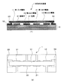
本発明のMEMS共振器1に係る実施例1を、図1(1)の概略構成断面図および図1(2)の平面レイアウト図によって説明する。
A first embodiment of the
図1に示すように、表面に絶縁膜52が形成された基板10上には、平衡で信号を入力する第1入力電極11と第2入力電極12および平衡で信号を出力する第1出力電極21と第2出力電極22が、第1入力電極11、第2出力電極22、第1出力電極21、第2入力電極12の順に並行に、かつ上記第1入力電極11と第1出力電極21のそれぞれの位置における後述する振動子31の振幅の位相が同位相となるように、また上記第2入力電極12と第2出力電極22のそれぞれの位置における振動子31の振幅の位相が同位相となるとともに上記第1入力電極11の位置における振動子31の位相とは180度異なる位相となるような位置に配置されている。
As shown in FIG. 1, a
また、上記第1入力電極11、第2出力電極22、第1出力電極21および第2入力電極12を挟むように振動子の電極33、34が形成されている。上記第1入力電極11、第2出力電極22、第1出力電極21および第2入力電極12上には、空間41を介して対向するように、かつ電極33、34に接続するように振動子31が形成されている。上記第1入力電極11、第2出力電極22、第1出力電極21および第2入力電極12と、振動子13との間の空間41は、例えば0.1μm程度に形成されている。
Further,
このように構成されたMEMS共振器1は、図2に示すような振動曲線を描いて振動子31は3次モードで振動する。この結果、MEMS共振器1は、入力in1から第1入力電極11に平衡で信号を入力し、その入力信号は第1出力電極21から出力out1へ信号を平衡で出力する。同様に、入力in2から第2入力電極12に平衡で信号を入力し、その入力信号は第2出力電極22から出力out2へ信号を平衡で出力する。このように、平衡で入力された信号は平衡で出力される。
The
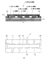
次に、本発明のMEMS共振器2に係る実施例2を、図3(1)の概略構成断面図および図3(2)の平面レイアウト図によって説明する。
Next, a second embodiment of the
図3に示すように、表面に絶縁膜(図示せず)が形成された基板10上には、平衡で信号を入力する第1入力電極11と第2入力電極12および平衡で信号を出力する第1出力電極21と第2出力電極22が、第1入力電極11、第2入力電極12、第1出力電極21、第2出力電極22の順に並行に、かつ上記第1入力電極11と第1出力電極21のそれぞれの位置における後述する振動子31の振幅の位相が同位相となるように、また上記第2入力電極12と第2出力電極22のそれぞれの位置における振動子31の振幅の位相が同位相となるとともに上記第1入力電極11の位置における振動子31の位相とは180度異なる位相となるような位置に配置されている。
As shown in FIG. 3, on a
また、上記第1入力電極11、第2入力電極12、第1出力電極21および第2出力電極22を挟むように振動子の電極33、34が形成されている。上記第1入力電極11、第2入力電極12、第1出力電極21および第2出力電極22上には、空間41を介して対向するように、かつ電極33、34に接続するように振動子31が形成されている。上記第1入力電極11、第2出力電極22、第1出力電極21および第2入力電極12と、振動子13との間の空間41は、例えば0.1μm程度に形成されている。
Further,
このように構成されたMEMS共振器2は、図4に示すような振動曲線を描いて振動子31は3次モードで振動する。この結果、MEMS共振器1は、入力in1から第1入力電極11に平衡で信号を入力し、その入力信号は第1出力電極21から出力out1へ信号を平衡で出力する。同様に、入力in2から第2入力電極12に平衡で信号を入力し、その入力信号は第2出力電極22から出力out2へ信号を平衡で出力する。このように、平衡で入力された信号は平衡で出力される。
The
上記実施例1および実施例2では4次モードのMEMS共振器を説明したが、本発明のMEMS共振器は、2n次モード(nは2以上の自然数)の振動を得るものとすることもできる。例えば、6次モードの振動を得るMEMS共振器の一例を、図5の概略構成断面図によって説明する。 In the first embodiment and the second embodiment, the fourth-order mode MEMS resonator has been described. However, the MEMS resonator of the present invention can obtain a vibration of a 2n-order mode (n is a natural number of 2 or more). . For example, an example of a MEMS resonator that obtains sixth-order mode vibration will be described with reference to the schematic cross-sectional view of FIG.
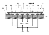
図5に示すように、表面に絶縁膜(図示せず)が形成された基板10上には、平衡で信号を入力する第1入力電極11と第2入力電極12と第3入力電極13と第4入力電極14、および平衡で信号を出力する第1出力電極21と第2出力電極22が、第1入力電極11、第2入力電極12、第1出力電極21、第2出力電極22、第3入力電極13、第4入力電極14の順に並行に、かつ上記第1入力電極11と第1出力電極21と第3入力電極13のそれぞれの位置における後述する振動子31の振幅の位相が同位相となるような位置に、また上記第2入力電極12と第2出力電極22と第4入力電極14のそれぞれの位置における振動子31の振幅の位相が同位相となるとともに上記第1入力電極11の位置における振動子31の位相とは180度異なる位相となるような位置に配置されている。
As shown in FIG. 5, a
また、上記第1入力電極11、第2入力電極12、第3入力電極13、第4入力電極14、第1出力電極21および第2出力電極22を挟むように振動子の電極33、34が形成されている。上記第1入力電極11、第2入力電極12、第3入力電極13、第4入力電極14、第1出力電極21および第2出力電極22上には、空間41を介して対向するように、かつ電極33、34に接続するように振動子31が形成されている。上記第1入力電極11、第1入力電極11、第1出力電極21、第2出力電極22、第3入力電極13および第4入力電極14と、振動子13との間の空間41は、例えば0.1μm程度に形成されている。
Further, the
このように構成されたMEMS共振器3は、図5に示すような振動曲線を描いて振動子31は6次モードで振動する。この結果、MEMS共振器1は、入力in1から第1入力電極11および第3入力電極13に平衡で信号を入力し、その入力信号は第1出力電極21から出力out1へ信号を平衡で出力する。同様に、入力in2から第2入力電極12および第4入力電極14に平衡で信号を入力し、その入力信号は第2出力電極22から出力out2へ信号を平衡で出力する。このように、平衡で入力された信号は平衡で出力される。
The
2n(nは2以上の自然数とする。)次の振動モードとなる本発明のMEMS共振器における各入力電極(第1入力電極、第2入力電極、第3入力電極、…)および各出力電極(第1出力電極、第2出力電極、第3出力電極、…)の配置位置は、下記のようになる。 2n (n is a natural number equal to or greater than 2) Each input electrode (first input electrode, second input electrode, third input electrode,...) And each output electrode in the MEMS resonator of the present invention in the next vibration mode. The arrangement positions of (first output electrode, second output electrode, third output electrode,...) Are as follows.
第1入力電極は2n個内の奇数番目に配置され、第1入力電極に入力された信号を出力する第1出力電極は2n個内の上記第1入力電極が配置された以外の奇数番目に配置される。また、第2入力電極は2n個内の偶数番目に配置され、第2入力電極に入力された信号を出力する第2出力電極は2n個内の上記第2入力電極が配置された以外の偶数番目に配置される。そして6次モード以上の場合には、さらに第3入力電極以降(第3入力電極、第4入力電極、…)の入力電極は上記第1入力電極と同一位相の場合には2n個内の空いている奇数番目に配置し、上記第2入力電極と同一位相の場合には2n個内の空いている偶数番目に配置し、第3出力電極以降(第3出力電極、第4出力電極、…)の出力電極は上記第1出力電極と同一位相の場合には2n個内の空いている奇数番目に配置し、上記第2出力電極と同一位相の場合には2n個内の空いている偶数番目に配置すればよい。 The first input electrodes are arranged in odd numbers in 2n, and the first output electrodes that output signals input to the first input electrodes are arranged in odd numbers other than the 2n first input electrodes are arranged. Be placed. In addition, the second input electrodes are arranged evenly in 2n, and the second output electrode that outputs a signal input to the second input electrode is an even number other than that in which the 2n second input electrodes are arranged. Placed in th. In the case of the 6th mode or higher, the input electrodes after the third input electrode (third input electrode, fourth input electrode,...) Are vacant in 2n when the same phase as the first input electrode. If the phase is the same as that of the second input electrode, it is arranged at an even number of 2n vacant and the third output electrode (third output electrode, fourth output electrode,... ) Are arranged in odd numbers within 2n when the phase is the same as that of the first output electrode, and even numbers within 2n when the phase is the same as that of the second output electrode. Just place it in the second.
上記説明したように、本発明のMEMS共振器は、入力電極に平衡で信号を入力し、その信号が出力電極から平衡で出力されるように、各入力電極、各出力電極が配置されるものであれば、2n次(nは2以上の自然数)のMEMS共振器とすることができる。このように高次モードのMEMS共振器では、振動子の長さが長くなるので、振動子の加工精度を高めることができる。なお、高次モードのMEMS共振器とするには、振動子やその支持部の耐久性を考慮して入力電極および出力電極の数を決定する必要がある。 As described above, the MEMS resonator of the present invention is configured such that each input electrode and each output electrode are arranged so that a signal is input to the input electrode in a balanced manner and the signal is output from the output electrode in a balanced manner. If so, a MEMS resonator of the 2nth order (n is a natural number of 2 or more) can be obtained. Thus, in the high-order mode MEMS resonator, the length of the vibrator becomes long, so that the processing accuracy of the vibrator can be increased. In order to obtain a high-order mode MEMS resonator, it is necessary to determine the number of input electrodes and output electrodes in consideration of the durability of the vibrator and its support.
次に、本発明のMEMS共振器1に係る製造方法の一例を、図6および図7の製造工程断面図によって説明する。
Next, an example of the manufacturing method according to the
図6(1)に示すように、半導体基板51に絶縁膜52を形成する。半導体基板51には、例えばシリコン基板を用い、絶縁膜52には、例えば窒化シリコン(SiN)膜を用いる。この窒化シリコン膜は、例えば1μmの厚さに形成する。なお、窒化シリコン膜の代わりに酸化シリコン膜と窒化シリコン膜との積層膜を用いてもよい。このように基板10は、一例としてシリコン基板51上に絶縁膜52が形成されたものからなる。さらに、絶縁膜52上に電極形成膜53を形成する。この電極形成膜53は、例えばポリシリコン膜で形成され、例えば0.5μmの厚さに形成される。
As shown in FIG. 6A, an insulating
次いで、図6(2)に示すように、レジスト塗布、リソグラフィー技術により入力電極形状および出力電極形状に上記電極形成膜53を加工するためのレジストマスクを形成した後、このレジストマスクを用いたエッチング加工により、上記電極形成膜53〔前記図6(1)参照〕で第1入力電極11と第2出力電極22と第1出力電極21と第2入力電極12とを形成する。同時に、上記電極形成膜53〔前記図6(1)参照〕で振動子の電極33、34も形成する。このとき、上記第1入力電極11と第1出力電極21とはそれぞれの位置における後に形成される振動子の振幅の位相が同位相となる位置に配置されるとともに、上記第2入力電極12と第2出力電極22とはそれぞれの位置における後に形成する振動子の振幅の位相が同位相となる位置でかつ上記第1入力電極11が形成される位置における後に形成する振動子の振幅の位相とは180度異なる位相となる位置に配置される。例えば、第1入力電極11、第2出力電極22、第1出力電極21、第2入力電極12の順に形成される。また、上記振動子の電極33、34は、第1入力電極11、第2出力電極22、第1出力電極21および第2入力電極12の電極群を、間隔を置いて挟むように形成される。上記第1、第2入力電極11,12、第1、第2出力電極21,22の配置は、入力信号が各入力電極に平衡入力され、出力信号が各出力電極より平衡出力される位置であればよい。
Next, as shown in FIG. 6B, a resist mask for processing the
次いで、図6(3)に示すように、上記第1入力電極11、第2出力電極22、第1出力電極21、第2入力電極12および振動子の電極34を被覆する様にかつ上記第1、第2入力電極11、12および第1、第2出力電極21、22よりも厚く犠牲層54を形成する。この犠牲層54は、例えば酸化シリコン膜で形成され、その厚さは例えば0.5μmとする。この犠牲層54は、上記絶縁膜52、各電極に対して選択的にエッチングされる材料であればよい。
Next, as shown in FIG. 6 (3), the
次いで、図6(4)に示すように、化学的機械研磨を用いて、上記犠牲層54の表面を平坦化する。このとき、上記第1、第2入力電極11、12上および第1、第2出力電極21、22上に、犠牲層54が薄く残るようにする。この残す厚さは、その後に形成される振動子と上記第1、第2入力電極11、12および第1、第2出力電極21、22との間隔を決定することになるので、その間隔分だけ残す。例えば、第1、第2入力電極11、12上および第1、第2出力電極21、22に犠牲層54が0.1μmの厚さだけ残るようにする。同様に、電極33、34上にも犠牲層54が残される。
Next, as shown in FIG. 6 (4), the surface of the
次いで、図7(5)に示すように、通常のレジスト塗布、リソグラフィー技術によるエッチングマスクの形成およびそのエッチングマスクを用いたエッチングにより、犠牲層54の一部をエッチング加工して上記電極33、34の一部を露出させる開口部55、56を形成する。
Next, as shown in FIG. 7 (5), a part of the
次いで、図7(6)に示すように、犠牲膜54が形成されている側の全面に振動子形成膜57を形成する。この振動子形成膜57は、例えばポリシリコン膜で形成し、例えば0.5μmの厚さに形成する。
Next, as shown in FIG. 7 (6), a
次いで、図7(7)に示すように、通常のレジスト塗布、リソグラフィー技術によるエッチングマスクの形成およびそのエッチングマスクを用いたエッチング加工により、振動子形成膜57をエッチング加工してビーム状の振動子31を形成する。この振動子31は、上記開口部55、56を通して電極33、34に接続されている。
Next, as shown in FIG. 7 (7), the vibrator-forming
次いで、図7(8)に示すように、ウエットエッチングによって、犠牲層54〔前記図7(7)参照〕をエッチング除去する。ここでは、犠牲層54を酸化シリコンで形成しているので、フッ酸を用いた。この結果、第1入力電極11、第2出力電極22、第1出力電極21、第2入力電極12の各両側、および第1入力電極11、第2出力電極22、第1出力電極21、第2入力電極12と振動子31との各間に空間41が形成される。この空間41は、第1入力電極11、第2出力電極22、第1出力電極21および第2入力電極12と振動子14との間の距離が0.1μm程度となっている。このようにして、MEMS共振器1が形成される。
Next, as shown in FIG. 7 (8), the sacrificial layer 54 [see FIG. 7 (7)] is removed by wet etching. Here, since the
上記製造方法において成膜される各膜の成膜方法は、CVD法、スパッタリング法、蒸着法等を採用することができる。また、上記した各膜厚は適宜設計されるものである。また、上記絶縁膜52の最表面を酸化シリコンで形成し、各電極をポリシリコンで形成した場合には、上記犠牲膜54は窒化シリコンで形成することができる。この場合の犠牲膜54のウエットエッチングは熱リン酸を用いればよい。
A CVD method, a sputtering method, a vapor deposition method, or the like can be adopted as a method for forming each film formed in the manufacturing method. Moreover, each above-mentioned film thickness is designed suitably. In the case where the outermost surface of the insulating
上記製造方法によれば、平衡入力を平衡出力することができる4次モードのMEMS共振器1を得ることができる。
According to the manufacturing method, it is possible to obtain the fourth-order
次に、本発明のMEMS共振器2に係る製造方法は、前記図6および図7の製造工程断面図によって説明した本発明のMEMS共振器1に係る製造方法において、第1入力電極11はそのまま第1入力電極とし、第2出力電極22の位置に第2入力電極を形成し、第1出力電極21はそのまま第1出力電極とし、第2入力電極12の位置に第2出力電極を形成すればよい。その他の工程は、実施例3で説明した製造工程と同様である。
Next, the manufacturing method according to the
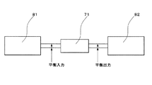
次に、本発明のMEMS共振器1もしくはMEMS共振器2を周波数フィルタに用いた実施例を、図8のブロック図によって説明する。
Next, an embodiment in which the
上記説明したように、本発明のMEMS共振器1は平衡入力が平衡出力となって出力されるため、この共振器1を周波数フィルタに用いた場合、不平衡出力を平衡出力とするバラン素子を用いる必要がない。すなわち、図8に示すように、本発明のMEMS共振器1を用いた周波数フィルタ71によって、前段デバイス(例えば集積回路)81からの出力信号(平衡入力)は平衡出力として出力される。そのため、周波数フィルタ71に直接、後段デバイス(例えば集積回路)82を接続することができる。
As described above, since the
上記MEMS共振器2、3も上記MEMS共振器1と同様に、前記図8によって説明した周波数フィルタに用いることができる。
Similarly to the
上記各実施例では、第1入力電極11、第2入力電極12、第1出力電極21、第2出力電極22、電極34等の各電極はポリシリコン以外に金属を用いることができる。この金属としては、例えばアルミニウム、金、銅、タングステン等の半導体装置に金属配線として用いる材料を用いることができる。
In each of the above embodiments, the
本発明のマイクロ電気機械システムの共振器およびその製造方法は、周波数フィルタ(RFフィルタ、IFフィルタ等)、発振器等の用途に適用できる。 The micro electro mechanical system resonator and the manufacturing method thereof according to the present invention can be applied to applications such as frequency filters (RF filters, IF filters, etc.), oscillators, and the like.
1…MEMS共振器、11…第1入力電極、12…第2入力電極、21…第1出力電極、22…第2出力電極、31…振動子、41…空間
DESCRIPTION OF
Claims (6)
信号を出力する出力電極と、
前記入力電極および前記出力電極に対して空間を介して対向する振動子と
を備えたマイクロ電気機械システムの共振器において、
前記入力電極に平衡で信号が入力され、
前記出力電極は平衡で信号が出力され、
前記入力電極は第1入力電極と第2入力電極とからなり、
前記出力電極は第1出力電極と第2出力電極とからなり、
前記第1入力電極と前記第1出力電極とはそれぞれの位置における前記振動子の振幅の位相が同位相となるように配置され、
第2入力電極と第2出力電極とはそれぞれの位置における前記振動子の振幅の位相が同位相の位置でかつ前記第1入力電極の位置における前記振動子の振幅の位相とは180度異なる位相となるように配置されている
ことを特徴とするマイクロ電気機械システムの共振器。 An input electrode for inputting a signal;
An output electrode for outputting a signal;
A vibrator facing the input electrode and the output electrode through a space;
In a resonator of a microelectromechanical system with
A signal is input to the input electrode in equilibrium,
The output electrode outputs a signal at equilibrium,
The input electrode comprises a first input electrode and a second input electrode,
The output electrode comprises a first output electrode and a second output electrode,
The first input electrode and the first output electrode are arranged such that the phase of the amplitude of the vibrator at each position is the same phase,
The second input electrode and the second output electrode have a phase of the amplitude of the vibrator at the same position and a phase that is 180 degrees different from the phase of the amplitude of the vibrator at the position of the first input electrode. It is arrange | positioned so that it may become. The resonator of the micro electro mechanical system characterized by the above-mentioned.
ことを特徴とする請求項1記載のマイクロ電気機械システムの共振器。 The first input electrode, the second output electrode, the first output electrode, the resonator of the microelectromechanical system according to claim 1, characterized in that it is arranged in order of the second input electrode.
ことを特徴とする請求項1記載のマイクロ電気機械システムの共振器。 The first input electrode, the second input electrode, the first output electrode, the resonator of the microelectromechanical system according to claim 1, characterized in that it is arranged in order of the second output electrode.
前記出力電極は複数個の出力電極からなり、
前記各入力電極のうちの第1入力電極と前記各出力電極のうちの第1出力電極とはそれぞれの位置における前記振動子の振幅の位相が同位相となるように配置され、
前記各入力電極のうちの第2入力電極と前記各出力電極のうちの第2出力電極とはそれぞれの位置における前記振動子の振幅の位相が同位相となるようにかつ前記第1入力電極の位置における前記振動子の振幅の位相とは180度異なる位相となるように配置され、
前記入力電極のうち残りの入力電極は前記第1入力電極もしくは前記第2入力電極の位置における前記振動子の振幅の位相と同位相となるように配置され、
前記出力電極のうち残りの出力電極は前記第1出力電極もしくは前記第2出力電極の位置における前記振動子の振幅の位相と同位相となるように配置される
ことを特徴とする請求項1記載のマイクロ電気機械システムの共振器。 The input electrode comprises a plurality of input electrodes,
The output electrode comprises a plurality of output electrodes,
The first input electrode of each of the input electrodes and the first output electrode of each of the output electrodes are arranged such that the phase of the amplitude of the vibrator at each position is the same phase,
The second input electrode of the input electrodes and the second output electrode of the output electrodes have the same phase of the amplitude of the vibrator at the respective positions, and Arranged so as to be 180 degrees different from the phase of the amplitude of the vibrator at the position,
Of the input electrodes, the remaining input electrodes are arranged to be in phase with the phase of the amplitude of the vibrator at the position of the first input electrode or the second input electrode,
Claim 1, wherein the remaining output electrode of the output electrode is characterized by being arranged such that the amplitude of the oscillator phase and same phase at the position of the first output electrode or said second output electrode Resonator of micro electro mechanical system.
信号を出力する出力電極と、
前記入力電極および前記出力電極に対して空間を介して対向する振動子と
を備えたマイクロ電気機械システムの共振器の製造方法において、
前記入力電極と前記出力電極とは同時に形成され、
前記入力電極には第1入力電極と第2入力電極とを形成し、
前記出力電極には第1出力電極と第2出力電極とを形成し、
前記第1入力電極と前記第1出力電極とはそれぞれの位置における前記振動子の振幅の位相が同位相となるように配置され、
第2入力電極と第2出力電極とはそれぞれの位置における前記振動子の振幅の位相が同位相となるようにかつ前記第1入力電極の位置における前記振動子の振幅の位相とは180度異なる位相となるように配置される
ことを特徴とするマイクロ電気機械システムの共振器の製造方法。 An input electrode for inputting a signal;
An output electrode for outputting a signal;
In a method of manufacturing a resonator of a microelectromechanical system comprising a vibrator facing the input electrode and the output electrode via a space,
The input electrode and the output electrode are formed simultaneously,
Forming a first input electrode and a second input electrode on the input electrode;
Forming a first output electrode and a second output electrode on the output electrode;
The first input electrode and the first output electrode are arranged such that the phase of the amplitude of the vibrator at each position is the same phase,
The second input electrode and the second output electrode are 180 degrees different from each other so that the phase of the amplitude of the vibrator at the respective positions is the same and the phase of the amplitude of the vibrator at the position of the first input electrode. A method for manufacturing a resonator of a microelectromechanical system, wherein the resonator is arranged so as to be in phase.
信号を出力する出力電極と、
前記入力電極および前記出力電極に対して空間を介して対向する振動子と
を備えたマイクロ電気機械システムの共振器を備えた周波数フィルタにおいて、
前記入力電極に平衡で信号が入力され、前記出力電極は平衡で信号が出力され、
前記入力電極は第1入力電極と第2入力電極とからなり、
前記出力電極は第1出力電極と第2出力電極とからなり、
前記第1入力電極と前記第1出力電極とはそれぞれの位置における前記振動子の振幅の位相が同位相となるように配置され、
第2入力電極と第2出力電極とはそれぞれの位置における前記振動子の振幅の位相が同位相の位置でかつ前記第1入力電極の位置における前記振動子の振幅の位相とは180度異なる位相となるように配置されている
ことを特徴とする周波数フィルタ。 An input electrode for inputting a signal;
An output electrode for outputting a signal;
A vibrator facing the input electrode and the output electrode through a space;
In a frequency filter with a resonator of a microelectromechanical system with
A signal is input to the input electrode at equilibrium, and a signal is output at the output electrode to balance,
The input electrode comprises a first input electrode and a second input electrode,
The output electrode comprises a first output electrode and a second output electrode,
The first input electrode and the first output electrode are arranged such that the phase of the amplitude of the vibrator at each position is the same phase,
The second input electrode and the second output electrode have a phase of the amplitude of the vibrator at the same position and a phase that is 180 degrees different from the phase of the amplitude of the vibrator at the position of the first input electrode. A frequency filter characterized by being arranged so that
Priority Applications (6)
| Application Number | Priority Date | Filing Date | Title |
|---|---|---|---|
| JP2004049133A JP4155209B2 (en) | 2004-02-25 | 2004-02-25 | Microelectromechanical system resonator, manufacturing method thereof, and frequency filter |
| EP04773394A EP1667323A1 (en) | 2003-09-19 | 2004-09-17 | Micro electric machine system resonator, drive method thereof, manufacturing method thereof, and frequency filter |
| PCT/JP2004/014010 WO2005029700A1 (en) | 2003-09-19 | 2004-09-17 | Micro electric machine system resonator, drive method thereof, manufacturing method thereof, and frequency filter |
| KR1020067005369A KR20060065720A (en) | 2003-09-19 | 2004-09-17 | Micro electric machine system resonator, drive method thereof, manufacturing method thereof, and frequency filter |
| TW093128108A TWI291450B (en) | 2003-09-19 | 2004-09-17 | Resonator for micro-electro-mechanical system, (MEMS), its driving method and frequency filter |
| US10/571,723 US20070010227A1 (en) | 2003-09-19 | 2004-09-17 | Micro electric machine system resonator, drive method thereof, manufacturing method thereof, and frequency filter |
Applications Claiming Priority (1)
| Application Number | Priority Date | Filing Date | Title |
|---|---|---|---|
| JP2004049133A JP4155209B2 (en) | 2004-02-25 | 2004-02-25 | Microelectromechanical system resonator, manufacturing method thereof, and frequency filter |
Publications (2)
| Publication Number | Publication Date |
|---|---|
| JP2005244406A JP2005244406A (en) | 2005-09-08 |
| JP4155209B2 true JP4155209B2 (en) | 2008-09-24 |
Family
ID=35025701
Family Applications (1)
| Application Number | Title | Priority Date | Filing Date |
|---|---|---|---|
| JP2004049133A Expired - Fee Related JP4155209B2 (en) | 2003-09-19 | 2004-02-25 | Microelectromechanical system resonator, manufacturing method thereof, and frequency filter |
Country Status (1)
| Country | Link |
|---|---|
| JP (1) | JP4155209B2 (en) |
Families Citing this family (2)
| Publication number | Priority date | Publication date | Assignee | Title |
|---|---|---|---|---|
| JP4736735B2 (en) * | 2005-11-15 | 2011-07-27 | ソニー株式会社 | Capacitance type resonance element, method for manufacturing capacitance type resonance element, and communication apparatus |
| JP2007150736A (en) * | 2005-11-28 | 2007-06-14 | Sony Corp | Micro electromechanical device |
-
2004
- 2004-02-25 JP JP2004049133A patent/JP4155209B2/en not_active Expired - Fee Related
Also Published As
| Publication number | Publication date |
|---|---|
| JP2005244406A (en) | 2005-09-08 |
Similar Documents
| Publication | Publication Date | Title |
|---|---|---|
| US7755454B2 (en) | Micro-electromechanical device | |
| US7498901B2 (en) | Filter device and transmitter-receiver utilizing beam-structured micro-resonators | |
| US7312674B2 (en) | Resonator system with a plurality of individual mechanically coupled resonators and method of making same | |
| JP4908156B2 (en) | Thin film piezoelectric vibrator, thin film piezoelectric bulk wave resonator and high frequency filter using the same | |
| TWI291450B (en) | Resonator for micro-electro-mechanical system, (MEMS), its driving method and frequency filter | |
| TWI309107B (en) | Micro-resonator, frequency filter and communication apparatus | |
| WO2007000929A1 (en) | Piezoelectric resonator, piezoelectric filter, resonator and communication device using the same | |
| US7489212B2 (en) | Microresonator, band-pass filter, semiconductor device, and communication apparatus | |
| JP2007013447A5 (en) | ||
| JP3982182B2 (en) | Surface acoustic wave device and manufacturing method thereof | |
| JP4341288B2 (en) | MEMS resonator, method of manufacturing the same, and filter | |
| JP4155209B2 (en) | Microelectromechanical system resonator, manufacturing method thereof, and frequency filter | |
| JP2005142852A (en) | Mems resonator | |
| JP2005167546A (en) | Electromechanical filter | |
| JP4254445B2 (en) | Microelectromechanical system resonator and driving method thereof | |
| JP2009088685A (en) | Electromechanical element, and semiconductor device | |
| JP2008177933A (en) | Electromechanical element, and signal processing device, communication equipment | |
| JP4040475B2 (en) | Micromechanical filter and portable information terminal | |
| Zuo et al. | Novel electrode configurations in dual-layer stacked and switchable ALN contour-mode resonators for low impedance filter termination and reduced insertion loss | |
| JP4389518B2 (en) | Micro-electromechanical system resonator and method for adjusting the same | |
| JP2005072757A (en) | Resonator of micro electromechanical system and drive method thereof | |
| KR100393774B1 (en) | Manufacturing method for bandpass filter using thin film bulk acoustic resonator | |
| JP2007142532A (en) | Static capacitance resonator, manufacturing method of the static capacitance resonator, and communication apparatus | |
| JP2005311568A (en) | Filter device and transceiver | |
| JP2005192146A (en) | Mems resonator and its manufacturing method |
Legal Events
| Date | Code | Title | Description |
|---|---|---|---|
| A131 | Notification of reasons for refusal |
Free format text: JAPANESE INTERMEDIATE CODE: A131 Effective date: 20071120 |
|
| A521 | Written amendment |
Free format text: JAPANESE INTERMEDIATE CODE: A523 Effective date: 20080111 |
|
| TRDD | Decision of grant or rejection written | ||
| A01 | Written decision to grant a patent or to grant a registration (utility model) |
Free format text: JAPANESE INTERMEDIATE CODE: A01 Effective date: 20080617 |
|
| A01 | Written decision to grant a patent or to grant a registration (utility model) |
Free format text: JAPANESE INTERMEDIATE CODE: A01 |
|
| A61 | First payment of annual fees (during grant procedure) |
Free format text: JAPANESE INTERMEDIATE CODE: A61 Effective date: 20080630 |
|
| FPAY | Renewal fee payment (event date is renewal date of database) |
Free format text: PAYMENT UNTIL: 20110718 Year of fee payment: 3 |
|
| FPAY | Renewal fee payment (event date is renewal date of database) |
Free format text: PAYMENT UNTIL: 20110718 Year of fee payment: 3 |
|
| LAPS | Cancellation because of no payment of annual fees |