EP1568655B1 - Micromachine and method of producing the same - Google Patents
Micromachine and method of producing the same Download PDFInfo
- Publication number
- EP1568655B1 EP1568655B1 EP03774185A EP03774185A EP1568655B1 EP 1568655 B1 EP1568655 B1 EP 1568655B1 EP 03774185 A EP03774185 A EP 03774185A EP 03774185 A EP03774185 A EP 03774185A EP 1568655 B1 EP1568655 B1 EP 1568655B1
- Authority
- EP
- European Patent Office
- Prior art keywords
- opening
- micromachine
- electrode
- insulating film
- interlayer insulating
- Prior art date
- Legal status (The legal status is an assumption and is not a legal conclusion. Google has not performed a legal analysis and makes no representation as to the accuracy of the status listed.)
- Expired - Lifetime
Links
Images


Classifications
-
- B—PERFORMING OPERATIONS; TRANSPORTING
- B81—MICROSTRUCTURAL TECHNOLOGY
- B81B—MICROSTRUCTURAL DEVICES OR SYSTEMS, e.g. MICROMECHANICAL DEVICES
- B81B3/00—Devices comprising flexible or deformable elements, e.g. comprising elastic tongues or membranes
-
- H—ELECTRICITY
- H03—ELECTRONIC CIRCUITRY
- H03H—IMPEDANCE NETWORKS, e.g. RESONANT CIRCUITS; RESONATORS
- H03H3/00—Apparatus or processes specially adapted for the manufacture of impedance networks, resonating circuits, resonators
- H03H3/007—Apparatus or processes specially adapted for the manufacture of impedance networks, resonating circuits, resonators for the manufacture of electromechanical resonators or networks
- H03H3/0072—Apparatus or processes specially adapted for the manufacture of impedance networks, resonating circuits, resonators for the manufacture of electromechanical resonators or networks of microelectro-mechanical resonators or networks
-
- B—PERFORMING OPERATIONS; TRANSPORTING
- B81—MICROSTRUCTURAL TECHNOLOGY
- B81C—PROCESSES OR APPARATUS SPECIALLY ADAPTED FOR THE MANUFACTURE OR TREATMENT OF MICROSTRUCTURAL DEVICES OR SYSTEMS
- B81C1/00—Manufacture or treatment of devices or systems in or on a substrate
-
- H—ELECTRICITY
- H03—ELECTRONIC CIRCUITRY
- H03H—IMPEDANCE NETWORKS, e.g. RESONANT CIRCUITS; RESONATORS
- H03H9/00—Networks comprising electromechanical or electro-acoustic elements; Electromechanical resonators
- H03H9/24—Constructional features of resonators of material which is not piezoelectric, electrostrictive, or magnetostrictive
- H03H9/2405—Constructional features of resonators of material which is not piezoelectric, electrostrictive, or magnetostrictive of microelectro-mechanical resonators
-
- H—ELECTRICITY
- H03—ELECTRONIC CIRCUITRY
- H03H—IMPEDANCE NETWORKS, e.g. RESONANT CIRCUITS; RESONATORS
- H03H9/00—Networks comprising electromechanical or electro-acoustic elements; Electromechanical resonators
- H03H9/02—Details
- H03H9/02244—Details of microelectro-mechanical resonators
- H03H2009/02488—Vibration modes
- H03H2009/02511—Vertical, i.e. perpendicular to the substrate plane
Definitions
- the present invention relates to a micromachine and a method for production thereof. More particularly, the present invention relates to a micromachine and a method for production thereof, the micromachine including the resonator electrode which traverses above the output electrode with a space interposed between them.
- micromachine technologies to form on a substrate (such as silicon substrate and glass substrate) microstructures and their control components (such as electrodes and semiconductor integrated circuits).
- Non-Patent Document 1 C.T.-C. Nguyen, "Micromechanical Components for Miniaturized Low-power Communications” (Invited Plenary Proceedings), 1999 IEEE MTT-S International Microwave Symposium RF MEMS Workshop, June, 18, 1999, pp. 48-77 .)
- a microresonator as a high-frequency filter for wireless communications.
- Fig. 14 shows such a microresonator 100, which is comprised of a substrate 101, an output electrode 102a, and a resonator electrode 103, with a space A interposed.
- the resonator electrode 103 has its one end connected to the input electrode 102b which is made of the same conductive layer as the output electrode 102a.
- the beam (vibrating part) 103a of the resonator electrode 103 (which is placed above the output electrode 102a, with a space A interposed) vibrates at a natural frequency.
- This vibration changes the capacity of the capacitor constructed of the space A between the output electrode 102a and the beam (vibrating part) 103a. This change is output through the output electrode 102a.
- the high-frequency filter relying on the microresonator 100 mentioned above realizes a higher Q-value than those relying on SAW (surface acoustic wave) or FBAR (film bulk acoustic resonator).
- a substrate 101 coated with an insulating film is prepared.
- On this substrate 101 are formed from polysilicon an output electrode 102a, an input electrode 102b, and a supporting electrode 102c.
- the first one 102a is held between the second and third ones 102b and 102c.
- the substrate 101 and the electrodes 102a to 102c are entirely covered with a sacrificial layer 105 of silicon oxide.
- contact holes 105b and 105c reaching the input electrode 102b and the supporting electrode 102c are made in the sacrificial layer 105. Then, a polysilicon layer 106 is formed on the sacrificial layer 105 and in the contact holes 105b and 105c.
- the polysilicon layer 106 undergoes pattern etching, so that a beltlike resonator electrode 103 passing above the output electrode 102a is formed.
- Pattern etching is performed in such a way that the contact holes 105b and 105c are kept covered completely for protection of the input electrode 102b and the supporting electrode 102c from etching.
- the sacrificial layer 105 is selectively removed to form a space A between the output electrode 102a and the resonator electrode 103.
- the microresonator 100 as shown in Fig. 14 .
- the microresonator 100 constructed as mentioned above has a natural frequency which depends on its beam length L (the length of the beam 103a) as shown in Fig. 16 . It is noted from Fig. 16 that the theoretical natural frequency according to the equation (1) below is proportional to 1/L 2 . This implies that it is necessary to reduce the beam length L in order to achieve a high natural frequency.
- f R 0.162 ⁇ h L 2 ⁇ EK ⁇
- h film thickness
- E Young's modulus
- K magnetic coupling ratio
- ⁇ film density
- the disadvantage of the above-mentioned microresonator 100 is that the beam length L cannot be made smaller than the width of the output electrode 102a because the space A and the resonator electrode 103 are formed over the output electrode 102a.
- the beam length L is to be reduced to increase the natural frequency, it is necessary to reduce the width of the output electrode 102a. This results in a decrease in capacity between the output electrode 102a and the resonator electrode 103, which in turn decreases output. This is the reason why it is impossible to increase the natural frequency by reducing the beam length L.
- JP-A-2231808 discloses an electrode structure of a crystal resonator.
- a recessed part is formed to one side of a crystal plate by dry etching or wet etching and an electrode is formed to the entire face of the recessed part forming face by vapour deposition and an electrode pattern similar to that of a conventional electrode is formed to the other flat face by photolithography.
- the electrode is formed to the entire flat face by vapour-deposition to prevent an open electrode at a step of the recessed part.
- WO 01/61848 A1 discloses a micromechanical tunable capacitor with high quality factor.
- a first conducting layer forms a first capacitor electrode and/or the electrodes to create an electrostatic force on the movable micromechanical structure.
- the above-mentioned object of the present invention is achieved by a micromachine which has an output electrode formed on a substrate and an interlayer insulating film formed on a substrate which has an opening whose bottom is the output electrode.
- a beltlike resonator electrode is so formed on the interlayer insulating film as to traverse above the space in the opening.
- the first micromachine according to the present invention is characterized in that the resonator electrode is concave to the opening along the side wall of the opening.
- the resonator electrode traversing the opening functions as the beam (or the vibrating part) of the resonator electrode. Therefore, the length of the vibrating part (or the beam length) is determined by the size of the opening irrespective of the width of the output electrode. Therefore, the resonator electrode may have the vibrating part which is shorter than the width of the output electrode.
- the lower surface of this resonator electrode is supported by the upper surface of the interlayer insulating film and the side of the vibrating part is supported by the side wall of the opening. Therefore, the resonator electrode is firmly supported by the interlayer insulating film, and this causes only the vibrating part to contribute to vibration.
- the vibrating part is made shorter as much as the thickness of the resonator electrode arranged along the side wall of the opening and consequently the substantial length of the vibrating part is shorter than the aperture size of the opening.
- the present invention is directed also to the method for producing the micromachine constructed as mentioned above.
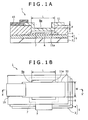
- Fig. 1A is a sectional view showing the structure of the micromachine according to the first embodiment
- Fig. 1B is a plan view showing the structure of the micromachine according to the first embodiment.
- the cross section in Fig. 1A is taken along the line X-X' in Fig.
- the micromachine 1 shown in these figures is formed on a substrate 5, which consists of a semiconductor substrate 3 and an insulating film 4 covering its surface. On the substrate 5 is formed a pattern of an output electrode 7. The output electrode 7 has a lead projecting from the micromachine 1 along the substrate 5.
- interlayer insulating film 9 which covers the output electrode 7.
- This interlayer insulating film 9 should preferably be formed flat in such a way as to embed the output electrode 7, although this is not limitative. It may cover the output electrode 7 with its surface configuration conforming to the placement of the output electrode 7.
- the interlayer insulating film 9 has an opening 9a reaching the output electrode 7. This opening 9a is positioned only above the output electrode 7 without protruding from the output electrode 7.
- the length L of the opening 9a is one of the factors that determine the frequency of the micromachine 1. Therefore, the opening 9a should have the length L which corresponds to the frequency required of the high-frequency filter constructed of the micromachine 1.
- the interlayer insulating film 9 On the interlayer insulating film 9 is a beltlike resonator electrode 11 which traverses the upper part of the space A in the opening 9a. That part of the resonator electrode 11 which coincides with the space A (or the opening 9a) functions as the vibrating part (beam) 11a.
- the length L of the opening 9a is the beam length L of the vibrating part (beam) 11a of the micromachine 1.
- the resonator electrode 11 is formed such that the vibrating part 11a is concave along the side wall of the opening 9a.
- the concave part of the resonator electrode 11 (or the center of the vibrating part 11a) is a certain distance (d) below from the upper surface of the interlayer insulating film 9.
- the value of d may be 0.2 ⁇ m, for instance.
- the lead 15 On the interlayer insulating film 9 is a lead 15 connected to the resonator electrode 11.
- the lead 15 may be formed from the same layer as the resonator electrode 11.
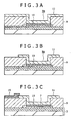
- the above-mentioned micromachine according to the first embodiment is produced by the method which is described below with reference to Figs. 2A to 2D and Figs. 3A to 3C (which are sectional views).
- a substrate 5 is prepared, which consists of a semiconductor substrate 3 (of single-crystal silicon) and an insulating film 4 covering it, as shown in Fig. 2A .
- the insulating film 4 should preferably be coated with a top layer made of a material which is resistant to etching to be performed subsequently on the sacrificial layer (e.g., silicon oxide). Therefore, the insulating film 4 is formed from a silicon oxide film 4a and a silicon nitride film 4b which are laminated on top of the other.
- the silicon oxide film 4a relieves stress between the upper layer and the semiconductor substrate 3.
- the silicon nitride film 4b is resistant to etching. These two films may be formed by low-pressure CVD, for instance.
- an output electrode 7 is formed on the substrate 5 by patterning a first conductive layer, as shown in Fig. 2B .
- the first conductive layer from which the output electrode 7 is formed should be a silicon layer of polysilicon containing phosphorus (P), for instance.
- the patterning of the first electrode layer and other parts (mentioned later) should be performed through a resist pattern (as a mask) formed by lithography.
- the substrate 5 and the output electrode 7 are covered with an interlayer insulating film 9, as shown in Fig. 2C .
- the interlayer insulating film 9 should be thick enough to completely cover the output electrode 7.
- the surface of the interlayer insulating film 9 should preferably be planarized subsequently.
- the interlayer insulating film 9 should be made of a material resistant to etching to be performed subsequently on the sacrificial layer. In the case where the sacrificial layer is formed from silicon oxide, the interlayer insulating film 9 should be formed from silicon nitride.
- the interlayer insulating film 9 does not need to have a flat surface that covers the output electrode 7. It may have a surface conforming to the shape of the output electrode 7.
- the interlayer insulating film 9 of silicon nitride may be formed by low-pressure CVD, for instance.
- An opening 9a (reaching the output electrode 7) is made in the interlayer insulating film 9.
- This opening 9a should have a shape which is within the configuration of the output electrode 7.
- the output electrode 7 constitutes the bottom of the opening 9a.
- the sacrificial layer 10 should be made of silicon oxide or the like, which can be selectively removed by subsequent etching, with no effect on the interlayer insulating film 9 and the output electrode 7.
- the sacrificial layer 10 of silicon oxide is formed by oxidizing the exposed surface of the output electrode 7 of polysilicon, with the interlayer insulating film 9 of silicon nitride masked.
- the sacrificial layer 10 should be formed in such a way that the surface of the sacrificial layer 10 is sufficiently lower than the surface of the interlayer insulating film 9 or the opening 9a remains concave even after the sacrificial layer 10 has been formed.
- a second conductive layer 12 is formed on the interlayer insulating film 9 in such a way that it covers the inside wall of the opening 9a whose bottom has been covered with the sacrificial layer 10, as shown in Fig. 3A .
- the second conductive layer 12 should be made of a material resistant to etching to be performed subsequently on the sacrificial layer 10. Consequently, it should be formed from polysilicon in the case where the sacrificial layer 10 is made of silicon oxide.
- the second conductive layer 12 should have a thickness which is established such that the surface which is concave to the opening 9a is lower than the surface of the interlayer insulating film 9.
- the second conductive layer 12 is patterned, so that the resonator electrode 11 is formed above the sacrificial layer 10 and the interlayer insulating film 9, as shown in Fig. 3B .
- the resonator electrode 11 should be formed in a beltlike pattern which traverses the sacrificial layer 10 and allows the opening 9a and the sacrificial layer 10 (formed in the opening 9a) to be partly exposed.
- the opening 9a may be exposed at both sides of the resonator electrode 11, as shown in Fig. 1B .
- the opening 9a and the sacrificial layer 10 may be exposed at one side in the W (width) direction (perpendicular to the beam length L) of the resonator electrode 11.
- the lead 15 connecting to the resonator electrode 11 is formed on the interlayer insulating film 9, as shown in Fig. 3C .
- This step may be carried out in the following manner. First, a seed layer of gold (Au) (not shown) is formed on the entire surface of the substrate 5. Next, a resist pattern (not shown) is formed which covers the seed layer excluding that part where the lead is to be formed. The lead 15 is formed by plating on the seed layer within the opening part of the resist pattern. The resist pattern is removed, and etching is performed on the entire surface to remove the seed layer. Incidentally, this step is not necessary in the case where the lead 15 and the resonator electrode 11 are formed from the same layer.
- the sacrificial layer 10 of silicon oxide (under the resonator electrode 11) is removed by selective wet etching with buffered hydrofluoric acid which leaves intact the lead 15, the resonator electrode 11, the interlayer insulting film 9, and the output electrode 7.
- the above-mentioned micromachine 1 has the resonator electrode 11 which traverses above the space A in the opening 9a formed in the interlayer insulting film 9.
- the beam 11a (vibrating part) of the resonator electrode 11 which traverses above the opening 9a) vibrates.
- the length of the vibrating part (or beam) 11a is determined by the size of the opening 9a.
- the advantage of the micromachine 1 according to the first embodiment, which is constructed as shown in Figs. 1A and 1B , is that the beam length L of the resonator electrode 11 can be reduced to the achievable minimum size of the opening 9a regardless of the line width of the output electrode 7. This advantage, however, is not gained by the related-art micromachine in which the space A and the resonator electrode 103 are arranged over the output electrode 102a, as explained above with reference to Fig. 14 .
- the resulting micromachine may be adaptable to higher frequencies owing to its much reduced beam length L.
- the micromachine 1 according to the first embodiment differs from the related-art micromachine shown in Fig. 14 in the capacity that occurs between the resonator electrode 11 and the output electrode 7.
- the former has a larger capacity for the same beam length L because of the large opposing area of the resonator electrode 11 and the output electrode 7. This implies that it maintains a high output even when the beam length L is reduced for high frequencies.
- the micromachine 1 is constructed as follows. Both ends of the resonator electrode 11 (or the anchors supporting the vibrating part 11a) are entirely fixed to the interlayer insulating film 9 and the sides of the vibrating part 11a are supported by the side wall of the opening 9a. This implies that the resonator electrode 11 is firmly supported by the interlayer insulting film 9 and only the vibrating part 11a efficiently contributes to vibration. As the result, a voltage of specific frequency applied to the micromachine 1 causes vibration to take place only in the beam (vibrating part) 11a of the resonator electrode 11. Consequently, the natural frequency is close to the theoretical value meeting the equation (1) given above (the value inversely proportional to the square of the length L of the vibrating part). This makes the micromachine 1 adaptive easily to high frequencies.
- micromachine 1 Another advantage of the micromachine 1 is that the vibrating part 11a of the resonator electrode 11 is shorter by its thickness placed along the side wall of the opening 9a. This implies that the length of the vibrating part which actually vibrates is shorter than the width of the opening 9a. This makes the micromachine 1 adaptive easily to high frequencies.
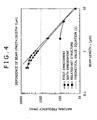
- Fig. 4 shows the result of simulation to predict how the natural frequency varies depending of the beam length L in the micromachine. It is to be noted that in the case of the micromachine according to the first embodiment, the dependence of natural frequency of the beam length is close to the theoretical value meeting the equation (1) given above. This result indicates that the micromachine 1 can be made to easily suit high frequencies by miniaturization.
- the anchor part supporting the beam (vibrating part) 103a has a projecting part B which is not in close contact with the underlying layer, and this projecting part B affects the vibration of the beam (vibrating part) 103a.
- the natural frequency decreases from the theoretical value meeting the equation (1) given above as the beam length L is reduced. This implies that the micromachine cannot be made to suit high frequencies by reducing the beam length L.
- micromachine 1 constructed according to the first embodiment can be used as a high-frequency filter with a high Q value.
- the advantage of planarizing the surface of the interlayer insulating film 9 (in which the output electrode 7 is embedded) is that the parasitic capacity (that part of capacity which does not contribute to vibration) which occurs between the resonator electrode 11 and the output electrode 7 is minimized, with the interlayer insulating film 9 interposed between them. Therefore, the micromachine 1 as a high-frequency filter can have an improved frequency selectivity (transmission property).
- the first embodiment has been explained above on the assumption that the width W of the resonator electrode 11 is the same, as shown in Fig. 1B .
- the resonator electrode 11 may be modified such that its both ends on the interlayer insulating film 9 are wider than its central part. This structure ensures the supporting of the beam (vibrating part) 11a.
- Fig. 5A is a sectional view showing the structure of the micromachine according to a second embodiment
- Fig. 5B is a plan view showing the structure of the micromachine according to the second embodiment.
- the cross section in Fig. 5A is taken along the line X-X' in Fig. 5B .
- the micromachine 20 according to the second embodiment is similar to the micromachine according to the first embodiment (which has been mentioned above with reference to Figs. 1A and 1B ) except for the structure of the resonator electrode 11'.
- the resonator electrode 11' of the micromachine 20 shown in Figs. 5A and 5B which is formed in the opening 9a has a width W large enough to cover the space A in the opening 9a made in the interlayer insulating film 9. It also has an opening 11b which reaches the space A. That part of the resonator electrode 11' which is above the space A and conforms to the opening 9a functions as the vibrating part 11a' as in the case of the micromachine according to the first embodiment.
- the resonator electrode 11' may have only one opening 11b (as shown) or two or more openings.
- the ratio of the area of the opening 11b to the area of the opening 9a and the arrangement and number of the opening 11b should be properly adjusted so that the micromachine 20 according to the second embodiment, which is used as a high-frequency filter, gives a desired output for a specific frequency range.
- the vibrating part 11a' of the resonator electrode 11' should be concave toward the opening 9a along the side wall of the opening 9a and the upper surface of the concave part (or the central part of the vibrating part 11a') should be lower than the top surface of the interlayer insulating film 9, with the difference being an arbitrary value indicated by d.
- the micromachine 20 which has the resonator electrode 11' constructed as mentioned above may be produced in a way similar to that of the first embodiment.
- the resonator electrode is formed which covers the opening 9a and has an opening which reaches the sacrificial layer 10 in the opening 9a, and the sacrificial layer 10 is selectively removed by etching through this opening.
- the micromachine according to the second embodiment which is constructed as mentioned above with reference to Figs. 5A and 5B , is characterized in that there is a space A in the opening 9a and the resonator electrode 11' is placed above it, and the resonator electrode 11' has an opening 11b communicating with the space A. Therefore, upon application of a voltage of specific frequency, the resonator electrode 11' (closing the opening 9a) vibrates, functioning as the vibrating part 11a'.
- the beam length L of the vibrating part 11a' is determined by the size of the opening 9a.
- the beam length L can be established according to the size of the opening 9a regardless of the width of the output electrode 7.
- the micromachine can be made adaptive to high frequencies by reducing the beam length L, while keeping the desired level of output.
- the resonator electrode 11' closes the opening 9a such that the beam (vibrating part) 11a' is firmly held by the interlayer insulating film 9 over the entire periphery. Moreover, both ends of the resonator electrode 11' (or the anchor parts supporting the beam (vibrating part) 11a') are fixed to the interlayer insulating film 9 over their entire surface and the side of the vibrating part 11a' is supported by the side wall of the opening 9a.
- This structure supports the resonator electrode 11' more firmly and hence adaptive to higher frequencies than the structure of the micromachine according to the first embodiment.
- Fig. 6 is a sectional view showing the structure of the micromachine according to a third embodiment.
- the micromachine 30 according to the third embodiment is similar to the micromachine according to the first embodiment (which has been mentioned above with reference to Figs. 1A and 1B ) except for the structure of the interlayer insulating film 31.
- the interlayer insulating film 31 which is so formed on the substrate 5 as to partly cover the output electrode 7, is composed of a first layer 32 and a second layer 33.
- the first layer 32 should have a sufficient thickness to embed the output electrode 7.
- the first layer 32 should preferably have a smooth surface, but this is not limitative. It may have an irregular shape conforming to the arrangement of the output electrode. It has an opening 32a reaching the output electrode 7. It is desirable that the opening 32a should not protrude from the output electrode 7 but be confined within the area of the output electrode 7, although this is not limitative.
- the second layer 33 is much thinner than the first layer 32. It is formed on the first layer 32 in such a way that it tightly covers the inner wall of the opening 32a of the first layer 32.
- the second layer 33 should be thick enough to protect the first layer 32, and its thickness should be equal to or slightly larger than the height of the space A placed under the resonator electrode 11.
- the second layer 32 has an opening 33a reaching the output electrode 7.
- the opening 33a is formed inside the opening 32a of the first layer 32. It is arranged above the output electrode 7, without projecting from the output electrode 7, and it is formed such that the first layer 32 is not exposed.
- the output electrode 7 is covered with the second layer 33 with a specific width (length).
- the resonator electrode 11 (which is formed on the interlayer insulating film 31 composed of the first layer 32 and the second layer 33) is concave toward the opening 32a along the side wall of the opening 32a in the first layer 32. In addition, the resonator electrode 11 traverses the space A in the opening 33a of the second layer 33. That part of the resonator electrode 11 which is above the space A (or which coincides with the opening 33a) functions as the vibrating part (beam) 11a.
- the resonator electrode 11 may be concave toward the opening 33a (or the space A) along the side wall of the opening 33a of the second layer 33.
- the resonator electrode 11 may be concave stepwise toward the output electrode 7, and the side of the vibrating part 11a is supported stepwise.
- the vibrating part 11a should preferably be formed such that the surface of its central part is lower by an arbitrary value (d) than the surface of the interlayer insulating film 31 (the second layer 33).
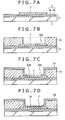
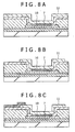
- the above-mentioned micromachine according to the third embodiment is produced by the method which is described below with reference to Figs. 7A to 7D and Figs. 8A to 8C (which are sectional views).
- a substrate 5 is prepared by coating a semiconductor substrate 3 with an insulating film 4 as shown in Fig. 7A .
- the output electrode 7. The steps up to this stage are the same as those explained above with reference to Figs. 2A and 2B .
- the first layer 32 of silicon oxide is formed which covers the output electrode 7 and the substrate 5, as shown in Fig. 7B .
- the first layer 32 should be thick enough to completely cover the output electrode 7, and it should be subsequently planarized.
- the opening 32a which reaches the output electrode 7.
- the second layer 33 which is sufficiently thinner than the first layer 32, is formed in such a way as to cover the inside wall of the opening 32a of the first layer 32, as shown in Fig. 7C .
- the second layer 33 should be formed from an insulating material which is resistant to etching to be performed subsequently on the sacrificial layer.
- the material for the second layer 33 may be silicon nitride if silicon oxide is used for the sacrificial layer.
- the opening 33a which reaches the output electrode 7.
- This opening 33a should be made such that it does not protrude from the output electrode 7; thus the output electrode 7 forms the bottom of the opening 33a.
- the sacrificial layer 10 is formed which covers the surface of the output electrode 7 which is exposed at the bottom of the opening 33a, as shown in Fig. 7D .
- the material for the sacrificial layer 10 is silicon oxide, for example, which can be selectively removed from the second layer 33 and the output electrode 7.
- the sacrificial layer 10 should be formed in the same way as explained in the first embodiment with reference to Fig. 2D . It is important that the sacrificial layer 10 should be formed such that its surface is barely or slightly lower than the surface of the second layer 33.
- Figs. 8A to 8C are carried out in the same way as the steps explained in the first embodiment with reference to Figs. 3A to 3C , provided that the removal of the sacrificial layer 10 is accomplished by selective etching for the lead 15, the resonator electrode 11, the second layer 33, and the output electrode 7.
- the foregoing steps yield the micromachine 30 as shown in Fig. 6 , which has the space A (which is left after removal of the sacrificial layer) under the resonator electrode 11 and which has the output electrode 7 (at the bottom of the opening 33a) which is exposed to the space A.
- the micromachine 30 also has the beltlike resonator electrode 11 which traverses the opening 33a above the space A in the opening 33a.
- the above-mentioned micromachine 30 according to the third embodiment has the resonator electrode 11 which traverses above the space A in the opening 33a, and the side of the beam (vibrating part) 11a of the resonator electrode 11 is supported by the side walls of the openings 32a and 33a. Therefore, it has a high Q value as in the case of the micromachine according to the first embodiment. It will find use as a high-frequency filter for higher frequency bands.
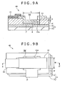
- Fig. 9A is a sectional view showing the structure of the micromachine according to a fourth embodiment
- Fig. 9B is a plan view showing the structure of the micromachine according to the fourth embodiment.
- the cross section in Fig. 9A is taken along the line X-X' in Fig. 9B .
- the micromachine 40 according to the fourth embodiment is similar to the micromachine according to the first embodiment (which has been mentioned above with reference to Figs. 1A and 1B ) except for the output electrode 7' which is formed in a groove.
- the micromachine 40 shown in Figs. 9A and 9B has the output electrode 7' which is formed in the opening 9a' of the interlayer insulating film 9', such that the upper surface of the output electrode 7' is entirely exposed from the interlayer insulating film 9'. Therefore, the opening 9a' in the interlayer insulating film 9' is formed such that the lead extending from the output electrode 7' is also exposed.
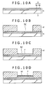
- micromachine according to the fourth embodiment is produced by the method which is described below with reference to Figs. 10A to 10D and Fig. 11 (which are sectional views).
- the substrate 5 is prepared by coating a semiconductor substrate 3 with an insulating film 4 in the same way as in the first embodiment which has been mentioned above with reference to Fig. 2A .
- the interlayer insulating film 9' is formed on the substrate 5, and then the opening 9a' (reaching the substrate 5 or the insulating film 4) is formed in the interlayer insulating film 9.
- the output electrode 7' is formed in the opening 9a'.
- a first conductive layer of polysilicon is formed on the interlayer insulating film 9' so as to fill the opening 9a', and then the first conductive layer on the interlayer insulating film 9' is removed by CMP process.
- the first conductive layer in the opening 9a' undergoes etch-back, so that the output electrode 7' of the first conductive layer is made sufficiently thinner than the interlayer insulating film 9'.
- the sacrificial layer 10 is selectively formed on the exposed surface of the output electrode 7' in the same way as in the first embodiment which has been mentioned above with reference to Fig. 2D .
- the ensuing steps are the same as those in the first embodiment which have been mentioned above with reference to Figs. 3A and 3C .
- the micromachine 40 which has been mentioned above with reference to Figs. 9A and 9B .
- the above-mentioned micromachine 40 according to the fourth embodiment has the resonator electrode 11 which traverses above the space A in the opening 9a', and the side of the beam (vibrating part) 11a of the resonator electrode 11 is supported by the side walls of the opening 9a'. Therefore, it has a high Q value as in the case of the micromachine according to the first embodiment. It will find use as a high-frequency filter for higher frequency bands.
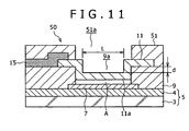
- Fig. 11 is a sectional view showing the structure of the micromachine according to a fifth embodiment.
- the micromachine 50 according to the fifth embodiment is similar to the micromachine according to the first embodiment (which has been mentioned above with reference to Figs. 1A and 1B ) except for the insulating film 51 which is additionally formed on the interlayer insulating film 9 in such a way as to cover the resonator electrode 11.
- the micromachine 50 has the resonator electrode 11 which is supported on the interlayer insulating film 9. In other words, both ends of the vibrating part 11a of the resonator electrode 11 are held between the interlayer insulating film 9 and the insulating film 51 placed thereon. The lead 15 is also held between the interlayer insulating film 9 and the insulating film 51.
- the interlayer insulating film 9 has an opening which is designated as a first opening 9a.
- the insulating film 51 placed on the interlayer insulating film 9 has an opening which is designated as a second opening 51a.
- the first opening 9a coincides approximately with the second opening 5a (in terms of shape and position).
- the second opening 51a should be large enough to permit the vibration of the vibrating part 11a.
- micromachine according to the fifth embodiment is produced by the method which is described below with reference to Figs. 12A and 12B (which are sectional views).
- the resonator electrode 11 and the lead 15 are formed on the interlayer insulating film 9 in the same way as in the first embodiment which has been explained above with reference to Figs. 2A to 2D and Figs. 3A to 3C .
- the insulating film 51 is formed on the interlayer insulating film 9 in such a way that it covers the resonator electrode 11 and the lead 15.
- the material for the insulating film 51 should be an insulating material, such as silicon nitride, which is resistant to etching to be performed subsequently on the sacrificial layer 10.
- the second opening 51a is formed in the insulating film 51.
- the second opening 51a overlaps with the first opening 9a in the interlayer insulating film 9.
- the sacrificial layer 10 of silicon oxide under the resonator electrode 11 is removed by selective wet etching with buffered hydrofluoric acid on the resonator electrode 11, the interlayer insulating film 9, the output electrode 7, and the insulating film 51.
- the selective etching forms the space A, prepared by removing the sacrificial layer, under the resonator electrode 11 and causes the output electrode 7 to be exposed at the bottom of the first opening 9a, as shown in Fig. 11 .
- the micromachine 50 which has the beltlike resonator electrode 11 which rests on the interlayer insulating film 9 and traverses the space A in the first opening 9a.
- the micromachine 50 according to the fifth embodiment which is constructed as mentioned above, has the resonator electrode 11 which closes the space A in the opening 9a in such a way that the side of the beam (vibrating part) 11a of the resonator electrode 11 is supported by the side wall of the opening 9a. Moreover, both ends of the vibrating part 11a of the resonator electrode 11 are held between the interlayer insulating film 9 and the insulating film 51 formed thereon.
- This structure supports the resonator electrode 11 more firmly than that in the first embodiment. Therefore, the micromachine according to the firth embodiment has a high Q value more certainly than in the case of the micromachine according to the first embodiment. It will find use as a high-frequency filter for higher frequency bands.
- Fig. 13 is a sectional view showing the structure of the micromachine according to a sixth embodiment.
- the micromachine 60 according to the sixth embodiment is a modification of the micromachine according to the fifth embodiment which has been mentioned above with reference to Fig. 11 .
- the micromachine 60 according to the sixth embodiment is similar to the micromachine according to the fifth embodiment except for the structure of the resonator electrode 61.
- the micromachine 60 is characterized in that the resonator electrode 61 does not have any part which is concave toward the output electrode 7 and its shape including its vibrating part 61a is flat and that the vibrating part 61a of the resonator electrode 61 has its both ends held between the interlayer insulating film 9 and the insulating film 51 thereon and the lead 15 is also held between the interlayer insulating film 9 and the insulating film 51.
- the micromachine 60 which has the resonator electrode 61 constructed as mentioned above may be produced in a way similar to that of the first embodiment.
- the sacrificial layer 10 which has been explained with reference to Fig. 2D
- the sacrificial layer 10 is formed as high as the opening 9a, and the subsequent steps are carried out in the same way as in the fifth embodiment.
- the micromachine 60 according to the sixth embodiment which is constructed as mentioned above with reference to Fig. 13 , has the resonator electrode 61 which traverses above the space A in the opening 9a. Therefore, as in the case of the first embodiment, when the resonator electrode 11 is caused to vibrate by application of a voltage of specific frequency, the vibrating part 61 traversing above the opening 9a vibrates and this part functions as the vibrating part 61a of the resonator electrode 61. It follows, therefore, that the length (beam length L) of the vibrating part 61a is determined by the size of the opening 9a.
- the micromachine 60 is adaptive to higher frequencies by reduction of the beam length L while maintaining the desired level of output.
- the micromachine 60 according to the sixth embodiment is constructed in the same way as in that according to the fifth embodiment. That is, both ends of the resonator electrode 61 (or the anchor parts supporting the vibrating part 61a) are held between the interlayer insulating film 9 and the insulating film 51 thereon. This means that the resonator electrode 61 is firmly supported by the interlayer insulating film 9 and the insulating film 51. Thus, only the vibrating part is made to contribute to vibration. As the result, when the resonator electrode 61 is caused to vibrate by application of a voltage of specific frequency, only the beam (vibrating part) 61a vibrates. Therefore, the natural frequency becomes closer to the theoretical value (inversely proportional to the square of the length L of the vibrating part) which meets the equation (1) given above. This easily makes the micromachine adaptive to high frequencies by miniaturization.
- Fig. 4 shows the result of simulation to predict how the natural frequency varies depending of the beam length L in the micromachine 60 according to the sixth embodiment. It is to be noted that in the case of the micromachine 60 according to the sixth embodiment, the dependence of natural frequency of the beam length is close to the theoretical value meeting the equation (1) given above. This result indicates that the micromachine 60 can be made to easily suit high frequencies by miniaturization.
- the resonator electrode 61 may have wide ends which ensure the supporting of the beam (vibrating part) 61a, so that the natural frequency increases further.
- the third to six embodiments may be combined with the second embodiment, so that the opening is closed by the resonator electrode. This enhances the effects of the third to sixth embodiments and increases the natural frequency by firmly supporting the resonator electrode.
- the present invention pertaining to the micromachine and its production method offers the advantage that the beam length or the length of the vibrating part of the resonator electrode can be made shorter than the width of the output electrode and yet the capacity between the output electrode and the resonator electrode can be made large relative to the length of the vibrating part, and the resonator electrode can be firmly supported by the interlayer insulating film.
- This permits the reduction of the beam length and causes the natural frequency to approach the theoretical value. Therefore, the resulting micromachine has a high Q value and is adaptive to high frequency bands.
Landscapes
- Engineering & Computer Science (AREA)
- Physics & Mathematics (AREA)
- Acoustics & Sound (AREA)
- Manufacturing & Machinery (AREA)
- Microelectronics & Electronic Packaging (AREA)
- Computer Hardware Design (AREA)
- Micromachines (AREA)
- Piezo-Electric Or Mechanical Vibrators, Or Delay Or Filter Circuits (AREA)
Description
- The present invention relates to a micromachine and a method for production thereof. More particularly, the present invention relates to a micromachine and a method for production thereof, the micromachine including the resonator electrode which traverses above the output electrode with a space interposed between them.
- With recent advance in the technology of microfabrication on a substrate, much attention is now focused on the micromachine technologies to form on a substrate (such as silicon substrate and glass substrate) microstructures and their control components (such as electrodes and semiconductor integrated circuits).
- One of such technologies is disclosed in Non-Patent
Document 1. (C.T.-C. Nguyen, "Micromechanical Components for Miniaturized Low-power Communications" (Invited Plenary Proceedings), 1999 IEEE MTT-S International Microwave Symposium RF MEMS Workshop, June, 18, 1999, pp. 48-77.) - The author of this literature proposes using a microresonator as a high-frequency filter for wireless communications.
Fig. 14 shows such amicroresonator 100, which is comprised of asubstrate 101, anoutput electrode 102a, and aresonator electrode 103, with a space A interposed. Theresonator electrode 103 has its one end connected to theinput electrode 102b which is made of the same conductive layer as theoutput electrode 102a. When a voltage with a specific frequency is applied to theinput electrode 102b, the beam (vibrating part) 103a of the resonator electrode 103 (which is placed above theoutput electrode 102a, with a space A interposed) vibrates at a natural frequency. This vibration changes the capacity of the capacitor constructed of the space A between theoutput electrode 102a and the beam (vibrating part) 103a. This change is output through theoutput electrode 102a. The high-frequency filter relying on themicroresonator 100 mentioned above realizes a higher Q-value than those relying on SAW (surface acoustic wave) or FBAR (film bulk acoustic resonator). - The microresonator mentioned above is produced in the following manner. First, referring to
Fig. 15A , asubstrate 101 coated with an insulating film is prepared. On thissubstrate 101 are formed from polysilicon anoutput electrode 102a, aninput electrode 102b, and a supportingelectrode 102c. Thefirst one 102a is held between the second andthird ones substrate 101 and theelectrodes 102a to 102c are entirely covered with asacrificial layer 105 of silicon oxide. - Second, referring to
Fig. 15B ,contact holes input electrode 102b and the supportingelectrode 102c are made in thesacrificial layer 105. Then, apolysilicon layer 106 is formed on thesacrificial layer 105 and in thecontact holes - Third, referring to
Fig. 15C , thepolysilicon layer 106 undergoes pattern etching, so that abeltlike resonator electrode 103 passing above theoutput electrode 102a is formed. Pattern etching is performed in such a way that thecontact holes input electrode 102b and the supportingelectrode 102c from etching. - Finally, the
sacrificial layer 105 is selectively removed to form a space A between theoutput electrode 102a and theresonator electrode 103. Thus, there is obtained themicroresonator 100 as shown inFig. 14 . - The
microresonator 100 constructed as mentioned above has a natural frequency which depends on its beam length L (the length of thebeam 103a) as shown inFig. 16 . It is noted fromFig. 16 that the theoretical natural frequency according to the equation (1) below is proportional to 1/L2. This implies that it is necessary to reduce the beam length L in order to achieve a high natural frequency.
where,
h: film thickness
E: Young's modulus
K: magnetic coupling ratio
ρ: film density - The disadvantage of the above-mentioned
microresonator 100 is that the beam length L cannot be made smaller than the width of theoutput electrode 102a because the space A and theresonator electrode 103 are formed over theoutput electrode 102a. - If the beam length L is to be reduced to increase the natural frequency, it is necessary to reduce the width of the
output electrode 102a. This results in a decrease in capacity between theoutput electrode 102a and theresonator electrode 103, which in turn decreases output. This is the reason why it is impossible to increase the natural frequency by reducing the beam length L. -
JP-A-2231808 -
WO 01/61848 A1 - It is an object of the present invention to provide a micromachine and a method for production thereof, the micromachine having a resonator electrode that makes it possible to increase the natural frequency by reducing the beam length.
- The above-mentioned object of the present invention is achieved by a micromachine which has an output electrode formed on a substrate and an interlayer insulating film formed on a substrate which has an opening whose bottom is the output electrode. A beltlike resonator electrode is so formed on the interlayer insulating film as to traverse above the space in the opening. The first micromachine according to the present invention is characterized in that the resonator electrode is concave to the opening along the side wall of the opening.
- In the first micromachine constructed as mentioned above, the resonator electrode traversing the opening functions as the beam (or the vibrating part) of the resonator electrode. Therefore, the length of the vibrating part (or the beam length) is determined by the size of the opening irrespective of the width of the output electrode. Therefore, the resonator electrode may have the vibrating part which is shorter than the width of the output electrode. In addition, the lower surface of this resonator electrode is supported by the upper surface of the interlayer insulating film and the side of the vibrating part is supported by the side wall of the opening. Therefore, the resonator electrode is firmly supported by the interlayer insulating film, and this causes only the vibrating part to contribute to vibration. Moreover, the vibrating part is made shorter as much as the thickness of the resonator electrode arranged along the side wall of the opening and consequently the substantial length of the vibrating part is shorter than the aperture size of the opening.
- The present invention is directed also to the method for producing the micromachine constructed as mentioned above.
- Only
Figures 1 to 12 show embodiments of the present invention. -
Figs. 1A and 1B are a sectional view and a plan view, respectively, of the micromachine according to a first embodiment of the present invention. -
Figs. 2A to 2D are sectional views showing the production method (part one) according to the first embodiment of the present invention. -
Figs. 3A to 3C are sectional views showing the production method (part two) according to the first embodiment of the present invention. -
Fig. 4 is a graph showing the result of simulation to predict how the beam length (L) affects the natural frequency. -
Figs. 5A and 5B are a sectional view and a plan view, respectively, of the micromachine according to a second embodiment of the present invention. -
Fig. 6 is a sectional view of the micromachine according to a third embodiment of the present invention. -
Figs. 7A to 7D are sectional views showing the production method (part one) according to the third embodiment of the present invention. -
Figs. 8A to 8C are sectional views showing the production method (part two) according to the third embodiment of the present invention. -
Figs. 9A and 9B are a sectional view and a plan view, respectively, of the micromachine according to a fourth embodiment of the present invention. -
Figs. 10A to 10D are sectional views showing the production method according to the fourth embodiment of the present invention. -
Fig. 11 is a sectional view of the micromachine according to a fifth embodiment of the present invention. -
Figs. 12A and 12B are sectional views showing the production method according to the fifth embodiment of the present invention. -
Fig. 13 is a sectional view of the micromachine according to a sixth embodiment of the present invention. -
Fig. 14 is a diagram showing the structure of a related-art micromachine (microresonator). -
Figs. 15A to 15C are sectional views showing the related-art production method. -
Fig. 16 is a graph illustrating the problems with the related-art micromachine. - In what follows, the embodiments of the present invention will be described in more detail with reference to the accompanying drawings. Each embodiment deals with the structure and production method of the micromachine as a microresonator suitable for use as a high-frequency filter.
-
Fig. 1A is a sectional view showing the structure of the micromachine according to the first embodiment, andFig. 1B is a plan view showing the structure of the micromachine according to the first embodiment. The cross section inFig. 1A is taken along the line X-X' in Fig. - The
micromachine 1 shown in these figures is formed on asubstrate 5, which consists of asemiconductor substrate 3 and an insulatingfilm 4 covering its surface. On thesubstrate 5 is formed a pattern of anoutput electrode 7. Theoutput electrode 7 has a lead projecting from themicromachine 1 along thesubstrate 5. - On the
substrate 5 is an interlayerinsulating film 9 which covers theoutput electrode 7. Thisinterlayer insulating film 9 should preferably be formed flat in such a way as to embed theoutput electrode 7, although this is not limitative. It may cover theoutput electrode 7 with its surface configuration conforming to the placement of theoutput electrode 7. - The
interlayer insulating film 9 has anopening 9a reaching theoutput electrode 7. Thisopening 9a is positioned only above theoutput electrode 7 without protruding from theoutput electrode 7. The length L of theopening 9a is one of the factors that determine the frequency of themicromachine 1. Therefore, theopening 9a should have the length L which corresponds to the frequency required of the high-frequency filter constructed of themicromachine 1. - On the
interlayer insulating film 9 is abeltlike resonator electrode 11 which traverses the upper part of the space A in theopening 9a. That part of theresonator electrode 11 which coincides with the space A (or theopening 9a) functions as the vibrating part (beam) 11a. In other words, the length L of theopening 9a is the beam length L of the vibrating part (beam) 11a of themicromachine 1. Theresonator electrode 11 is formed such that the vibratingpart 11a is concave along the side wall of theopening 9a. The concave part of the resonator electrode 11 (or the center of the vibratingpart 11a) is a certain distance (d) below from the upper surface of theinterlayer insulating film 9. The value of d may be 0.2 µm, for instance. - On the
interlayer insulating film 9 is a lead 15 connected to theresonator electrode 11. Incidentally, thelead 15 may be formed from the same layer as theresonator electrode 11. - The above-mentioned micromachine according to the first embodiment is produced by the method which is described below with reference to
Figs. 2A to 2D andFigs. 3A to 3C (which are sectional views). - First, a
substrate 5 is prepared, which consists of a semiconductor substrate 3 (of single-crystal silicon) and an insulatingfilm 4 covering it, as shown inFig. 2A . The insulatingfilm 4 should preferably be coated with a top layer made of a material which is resistant to etching to be performed subsequently on the sacrificial layer (e.g., silicon oxide). Therefore, the insulatingfilm 4 is formed from asilicon oxide film 4a and asilicon nitride film 4b which are laminated on top of the other. Thesilicon oxide film 4a relieves stress between the upper layer and thesemiconductor substrate 3. Thesilicon nitride film 4b is resistant to etching. These two films may be formed by low-pressure CVD, for instance. - Next, an
output electrode 7 is formed on thesubstrate 5 by patterning a first conductive layer, as shown inFig. 2B . The first conductive layer from which theoutput electrode 7 is formed should be a silicon layer of polysilicon containing phosphorus (P), for instance. The patterning of the first electrode layer and other parts (mentioned later) should be performed through a resist pattern (as a mask) formed by lithography. - The
substrate 5 and theoutput electrode 7 are covered with aninterlayer insulating film 9, as shown inFig. 2C . Theinterlayer insulating film 9 should be thick enough to completely cover theoutput electrode 7. The surface of theinterlayer insulating film 9 should preferably be planarized subsequently. Theinterlayer insulating film 9 should be made of a material resistant to etching to be performed subsequently on the sacrificial layer. In the case where the sacrificial layer is formed from silicon oxide, theinterlayer insulating film 9 should be formed from silicon nitride. Incidentally, theinterlayer insulating film 9 does not need to have a flat surface that covers theoutput electrode 7. It may have a surface conforming to the shape of theoutput electrode 7. Theinterlayer insulating film 9 of silicon nitride may be formed by low-pressure CVD, for instance. - An
opening 9a (reaching the output electrode 7) is made in theinterlayer insulating film 9. Thisopening 9a should have a shape which is within the configuration of theoutput electrode 7. Thus, theoutput electrode 7 constitutes the bottom of theopening 9a. - That part of the
output electrode 7 which is exposed at the bottom of theopening 9a is covered with thesacrificial layer 10, as shown inFig. 2D . Thesacrificial layer 10 should be made of silicon oxide or the like, which can be selectively removed by subsequent etching, with no effect on theinterlayer insulating film 9 and theoutput electrode 7. In practice, thesacrificial layer 10 of silicon oxide is formed by oxidizing the exposed surface of theoutput electrode 7 of polysilicon, with theinterlayer insulating film 9 of silicon nitride masked. It is important that thesacrificial layer 10 should be formed in such a way that the surface of thesacrificial layer 10 is sufficiently lower than the surface of theinterlayer insulating film 9 or theopening 9a remains concave even after thesacrificial layer 10 has been formed. - A second
conductive layer 12 is formed on theinterlayer insulating film 9 in such a way that it covers the inside wall of theopening 9a whose bottom has been covered with thesacrificial layer 10, as shown inFig. 3A . The secondconductive layer 12 should be made of a material resistant to etching to be performed subsequently on thesacrificial layer 10. Consequently, it should be formed from polysilicon in the case where thesacrificial layer 10 is made of silicon oxide. The secondconductive layer 12 should have a thickness which is established such that the surface which is concave to theopening 9a is lower than the surface of theinterlayer insulating film 9. - The second
conductive layer 12 is patterned, so that theresonator electrode 11 is formed above thesacrificial layer 10 and theinterlayer insulating film 9, as shown inFig. 3B . Theresonator electrode 11 should be formed in a beltlike pattern which traverses thesacrificial layer 10 and allows theopening 9a and the sacrificial layer 10 (formed in theopening 9a) to be partly exposed. Theopening 9a may be exposed at both sides of theresonator electrode 11, as shown inFig. 1B . Alternatively, theopening 9a and thesacrificial layer 10 may be exposed at one side in the W (width) direction (perpendicular to the beam length L) of theresonator electrode 11. - The
lead 15 connecting to theresonator electrode 11 is formed on theinterlayer insulating film 9, as shown inFig. 3C . This step may be carried out in the following manner. First, a seed layer of gold (Au) (not shown) is formed on the entire surface of thesubstrate 5. Next, a resist pattern (not shown) is formed which covers the seed layer excluding that part where the lead is to be formed. Thelead 15 is formed by plating on the seed layer within the opening part of the resist pattern. The resist pattern is removed, and etching is performed on the entire surface to remove the seed layer. Incidentally, this step is not necessary in the case where thelead 15 and theresonator electrode 11 are formed from the same layer. - The
sacrificial layer 10 of silicon oxide (under the resonator electrode 11) is removed by selective wet etching with buffered hydrofluoric acid which leaves intact thelead 15, theresonator electrode 11, the interlayerinsulting film 9, and theoutput electrode 7. - The foregoing steps form the space A under the
resonator electrode 11 and cause theoutput electrode 7 to be exposed at the bottom of theopening 9a, as shown inFigs. 1A and 1B . In this way there is obtained themicromachine 1 which has thebeltlike resonator electrode 11 traversing above theinterlayer insulating film 9 and the space A in theopening 9a. - The above-mentioned
micromachine 1 according to the first embodiment has theresonator electrode 11 which traverses above the space A in theopening 9a formed in the interlayerinsulting film 9. Upon application of a voltage of specific frequency, thebeam 11a (vibrating part) of the resonator electrode 11 (which traverses above theopening 9a) vibrates. Thus, the length of the vibrating part (or beam) 11a (beam length L) is determined by the size of theopening 9a. - The advantage of the
micromachine 1 according to the first embodiment, which is constructed as shown inFigs. 1A and 1B , is that the beam length L of theresonator electrode 11 can be reduced to the achievable minimum size of theopening 9a regardless of the line width of theoutput electrode 7. This advantage, however, is not gained by the related-art micromachine in which the space A and theresonator electrode 103 are arranged over theoutput electrode 102a, as explained above with reference toFig. 14 . The resulting micromachine may be adaptable to higher frequencies owing to its much reduced beam length L. - The
micromachine 1 according to the first embodiment differs from the related-art micromachine shown inFig. 14 in the capacity that occurs between theresonator electrode 11 and theoutput electrode 7. The former has a larger capacity for the same beam length L because of the large opposing area of theresonator electrode 11 and theoutput electrode 7. This implies that it maintains a high output even when the beam length L is reduced for high frequencies. - The
micromachine 1 according to the first embodiment is constructed as follows. Both ends of the resonator electrode 11 (or the anchors supporting the vibratingpart 11a) are entirely fixed to theinterlayer insulating film 9 and the sides of the vibratingpart 11a are supported by the side wall of theopening 9a. This implies that theresonator electrode 11 is firmly supported by the interlayerinsulting film 9 and only the vibratingpart 11a efficiently contributes to vibration. As the result, a voltage of specific frequency applied to themicromachine 1 causes vibration to take place only in the beam (vibrating part) 11a of theresonator electrode 11. Consequently, the natural frequency is close to the theoretical value meeting the equation (1) given above (the value inversely proportional to the square of the length L of the vibrating part). This makes themicromachine 1 adaptive easily to high frequencies. - Another advantage of the
micromachine 1 is that the vibratingpart 11a of theresonator electrode 11 is shorter by its thickness placed along the side wall of theopening 9a. This implies that the length of the vibrating part which actually vibrates is shorter than the width of theopening 9a. This makes themicromachine 1 adaptive easily to high frequencies. -
Fig. 4 shows the result of simulation to predict how the natural frequency varies depending of the beam length L in the micromachine. It is to be noted that in the case of the micromachine according to the first embodiment, the dependence of natural frequency of the beam length is close to the theoretical value meeting the equation (1) given above. This result indicates that themicromachine 1 can be made to easily suit high frequencies by miniaturization. - The foregoing does not apply to the related-art micromachine shown in
Fig. 14 because of its structure restricted by its manufacturing process. That is, the anchor part supporting the beam (vibrating part) 103a has a projecting part B which is not in close contact with the underlying layer, and this projecting part B affects the vibration of the beam (vibrating part) 103a. This is evident from the fact that the natural frequency decreases from the theoretical value meeting the equation (1) given above as the beam length L is reduced. This implies that the micromachine cannot be made to suit high frequencies by reducing the beam length L. - It is concluded from the foregoing that the
micromachine 1 constructed according to the first embodiment can be used as a high-frequency filter with a high Q value. - The advantage of planarizing the surface of the interlayer insulating film 9 (in which the
output electrode 7 is embedded) is that the parasitic capacity (that part of capacity which does not contribute to vibration) which occurs between theresonator electrode 11 and theoutput electrode 7 is minimized, with theinterlayer insulating film 9 interposed between them. Therefore, themicromachine 1 as a high-frequency filter can have an improved frequency selectivity (transmission property). - Incidentally, the first embodiment has been explained above on the assumption that the width W of the
resonator electrode 11 is the same, as shown inFig. 1B . However, theresonator electrode 11 may be modified such that its both ends on theinterlayer insulating film 9 are wider than its central part. This structure ensures the supporting of the beam (vibrating part) 11a. -
Fig. 5A is a sectional view showing the structure of the micromachine according to a second embodiment, andFig. 5B is a plan view showing the structure of the micromachine according to the second embodiment. The cross section inFig. 5A is taken along the line X-X' inFig. 5B . - The
micromachine 20 according to the second embodiment is similar to the micromachine according to the first embodiment (which has been mentioned above with reference toFigs. 1A and 1B ) except for the structure of the resonator electrode 11'. - The resonator electrode 11' of the
micromachine 20 shown inFigs. 5A and 5B , which is formed in theopening 9a has a width W large enough to cover the space A in theopening 9a made in theinterlayer insulating film 9. It also has anopening 11b which reaches the space A. That part of the resonator electrode 11' which is above the space A and conforms to theopening 9a functions as the vibratingpart 11a' as in the case of the micromachine according to the first embodiment. - The resonator electrode 11' may have only one
opening 11b (as shown) or two or more openings. The ratio of the area of theopening 11b to the area of theopening 9a and the arrangement and number of theopening 11b should be properly adjusted so that themicromachine 20 according to the second embodiment, which is used as a high-frequency filter, gives a desired output for a specific frequency range. - In the same way as in the first embodiment, the vibrating
part 11a' of the resonator electrode 11' should be concave toward theopening 9a along the side wall of theopening 9a and the upper surface of the concave part (or the central part of the vibratingpart 11a') should be lower than the top surface of theinterlayer insulating film 9, with the difference being an arbitrary value indicated by d. - The
micromachine 20 which has the resonator electrode 11' constructed as mentioned above may be produced in a way similar to that of the first embodiment. In the step of forming the resonator electrode shown inFig. 3B , the resonator electrode is formed which covers theopening 9a and has an opening which reaches thesacrificial layer 10 in theopening 9a, and thesacrificial layer 10 is selectively removed by etching through this opening. - The micromachine according to the second embodiment, which is constructed as mentioned above with reference to
Figs. 5A and 5B , is characterized in that there is a space A in theopening 9a and the resonator electrode 11' is placed above it, and the resonator electrode 11' has anopening 11b communicating with the space A. Therefore, upon application of a voltage of specific frequency, the resonator electrode 11' (closing theopening 9a) vibrates, functioning as the vibratingpart 11a'. The beam length L of the vibratingpart 11a' is determined by the size of theopening 9a. As in the case of the micromachine according to the first embodiment, the beam length L can be established according to the size of theopening 9a regardless of the width of theoutput electrode 7. Thus, the micromachine can be made adaptive to high frequencies by reducing the beam length L, while keeping the desired level of output. - Another feature of the
micromachine 20 according to the second embodiment is that the resonator electrode 11' closes theopening 9a such that the beam (vibrating part) 11a' is firmly held by theinterlayer insulating film 9 over the entire periphery. Moreover, both ends of the resonator electrode 11' (or the anchor parts supporting the beam (vibrating part) 11a') are fixed to theinterlayer insulating film 9 over their entire surface and the side of the vibratingpart 11a' is supported by the side wall of theopening 9a. This structure supports the resonator electrode 11' more firmly and hence adaptive to higher frequencies than the structure of the micromachine according to the first embodiment. -
Fig. 6 is a sectional view showing the structure of the micromachine according to a third embodiment. Themicromachine 30 according to the third embodiment is similar to the micromachine according to the first embodiment (which has been mentioned above with reference toFigs. 1A and 1B ) except for the structure of theinterlayer insulating film 31. - In the
micromachine 30, theinterlayer insulating film 31, which is so formed on thesubstrate 5 as to partly cover theoutput electrode 7, is composed of afirst layer 32 and asecond layer 33. - The
first layer 32 should have a sufficient thickness to embed theoutput electrode 7. Thefirst layer 32 should preferably have a smooth surface, but this is not limitative. It may have an irregular shape conforming to the arrangement of the output electrode. It has anopening 32a reaching theoutput electrode 7. It is desirable that theopening 32a should not protrude from theoutput electrode 7 but be confined within the area of theoutput electrode 7, although this is not limitative. - The
second layer 33 is much thinner than thefirst layer 32. It is formed on thefirst layer 32 in such a way that it tightly covers the inner wall of theopening 32a of thefirst layer 32. Thesecond layer 33 should be thick enough to protect thefirst layer 32, and its thickness should be equal to or slightly larger than the height of the space A placed under theresonator electrode 11. Thesecond layer 32 has anopening 33a reaching theoutput electrode 7. Theopening 33a is formed inside theopening 32a of thefirst layer 32. It is arranged above theoutput electrode 7, without projecting from theoutput electrode 7, and it is formed such that thefirst layer 32 is not exposed. Theoutput electrode 7 is covered with thesecond layer 33 with a specific width (length). - The resonator electrode 11 (which is formed on the
interlayer insulating film 31 composed of thefirst layer 32 and the second layer 33) is concave toward theopening 32a along the side wall of theopening 32a in thefirst layer 32. In addition, theresonator electrode 11 traverses the space A in theopening 33a of thesecond layer 33. That part of theresonator electrode 11 which is above the space A (or which coincides with theopening 33a) functions as the vibrating part (beam) 11a. - The
resonator electrode 11 may be concave toward theopening 33a (or the space A) along the side wall of theopening 33a of thesecond layer 33. In this case, theresonator electrode 11 may be concave stepwise toward theoutput electrode 7, and the side of the vibratingpart 11a is supported stepwise. Incidentally, as in the first embodiment, the vibratingpart 11a should preferably be formed such that the surface of its central part is lower by an arbitrary value (d) than the surface of the interlayer insulating film 31 (the second layer 33). - The above-mentioned micromachine according to the third embodiment is produced by the method which is described below with reference to
Figs. 7A to 7D andFigs. 8A to 8C (which are sectional views). - First, a
substrate 5 is prepared by coating asemiconductor substrate 3 with an insulatingfilm 4 as shown inFig. 7A . On thesubstrate 5 is formed theoutput electrode 7. The steps up to this stage are the same as those explained above with reference toFigs. 2A and 2B . - Next, the
first layer 32 of silicon oxide is formed which covers theoutput electrode 7 and thesubstrate 5, as shown inFig. 7B . Thefirst layer 32 should be thick enough to completely cover theoutput electrode 7, and it should be subsequently planarized. In thefirst layer 32 is made theopening 32a which reaches theoutput electrode 7. - The
second layer 33, which is sufficiently thinner than thefirst layer 32, is formed in such a way as to cover the inside wall of theopening 32a of thefirst layer 32, as shown inFig. 7C . Thesecond layer 33 should be formed from an insulating material which is resistant to etching to be performed subsequently on the sacrificial layer. The material for thesecond layer 33 may be silicon nitride if silicon oxide is used for the sacrificial layer. - In the
second layer 33 is formed theopening 33a which reaches theoutput electrode 7. Thisopening 33a should be made such that it does not protrude from theoutput electrode 7; thus theoutput electrode 7 forms the bottom of theopening 33a. - Then, the
sacrificial layer 10 is formed which covers the surface of theoutput electrode 7 which is exposed at the bottom of theopening 33a, as shown inFig. 7D . The material for thesacrificial layer 10 is silicon oxide, for example, which can be selectively removed from thesecond layer 33 and theoutput electrode 7. Thesacrificial layer 10 should be formed in the same way as explained in the first embodiment with reference toFig. 2D . It is important that thesacrificial layer 10 should be formed such that its surface is barely or slightly lower than the surface of thesecond layer 33. - The subsequent steps shown in
Figs. 8A to 8C are carried out in the same way as the steps explained in the first embodiment with reference toFigs. 3A to 3C , provided that the removal of thesacrificial layer 10 is accomplished by selective etching for thelead 15, theresonator electrode 11, thesecond layer 33, and theoutput electrode 7. - The foregoing steps yield the
micromachine 30 as shown inFig. 6 , which has the space A (which is left after removal of the sacrificial layer) under theresonator electrode 11 and which has the output electrode 7 (at the bottom of theopening 33a) which is exposed to the space A. Themicromachine 30 also has thebeltlike resonator electrode 11 which traverses theopening 33a above the space A in theopening 33a. - The above-mentioned
micromachine 30 according to the third embodiment has theresonator electrode 11 which traverses above the space A in theopening 33a, and the side of the beam (vibrating part) 11a of theresonator electrode 11 is supported by the side walls of theopenings -
Fig. 9A is a sectional view showing the structure of the micromachine according to a fourth embodiment, andFig. 9B is a plan view showing the structure of the micromachine according to the fourth embodiment. The cross section inFig. 9A is taken along the line X-X' inFig. 9B . - The
micromachine 40 according to the fourth embodiment is similar to the micromachine according to the first embodiment (which has been mentioned above with reference toFigs. 1A and 1B ) except for the output electrode 7' which is formed in a groove. - The
micromachine 40 shown inFigs. 9A and 9B has the output electrode 7' which is formed in theopening 9a' of the interlayer insulating film 9', such that the upper surface of the output electrode 7' is entirely exposed from the interlayer insulating film 9'. Therefore, theopening 9a' in the interlayer insulating film 9' is formed such that the lead extending from the output electrode 7' is also exposed. - The above-mentioned micromachine according to the fourth embodiment is produced by the method which is described below with reference to
Figs. 10A to 10D andFig. 11 (which are sectional views). - In the first step shown in
Fig. 10A , thesubstrate 5 is prepared by coating asemiconductor substrate 3 with an insulatingfilm 4 in the same way as in the first embodiment which has been mentioned above with reference toFig. 2A . - In the next step shown in
Fig. 10B , the interlayer insulating film 9' is formed on thesubstrate 5, and then theopening 9a' (reaching thesubstrate 5 or the insulating film 4) is formed in theinterlayer insulating film 9. - In the subsequent step shown in
Fig. 10C , the output electrode 7' is formed in theopening 9a'. In practice, a first conductive layer of polysilicon is formed on the interlayer insulating film 9' so as to fill theopening 9a', and then the first conductive layer on the interlayer insulating film 9' is removed by CMP process. The first conductive layer in theopening 9a' undergoes etch-back, so that the output electrode 7' of the first conductive layer is made sufficiently thinner than the interlayer insulating film 9'. - In the next step shown in
Fig. 10D , thesacrificial layer 10 is selectively formed on the exposed surface of the output electrode 7' in the same way as in the first embodiment which has been mentioned above with reference toFig. 2D . The ensuing steps are the same as those in the first embodiment which have been mentioned above with reference toFigs. 3A and 3C . In this way there is obtained themicromachine 40 which has been mentioned above with reference toFigs. 9A and 9B . - The above-mentioned
micromachine 40 according to the fourth embodiment has theresonator electrode 11 which traverses above the space A in theopening 9a', and the side of the beam (vibrating part) 11a of theresonator electrode 11 is supported by the side walls of theopening 9a'. Therefore, it has a high Q value as in the case of the micromachine according to the first embodiment. It will find use as a high-frequency filter for higher frequency bands. -
Fig. 11 is a sectional view showing the structure of the micromachine according to a fifth embodiment. Themicromachine 50 according to the fifth embodiment is similar to the micromachine according to the first embodiment (which has been mentioned above with reference toFigs. 1A and 1B ) except for the insulatingfilm 51 which is additionally formed on theinterlayer insulating film 9 in such a way as to cover theresonator electrode 11. - The
micromachine 50 has theresonator electrode 11 which is supported on theinterlayer insulating film 9. In other words, both ends of the vibratingpart 11a of theresonator electrode 11 are held between the interlayer insulatingfilm 9 and the insulatingfilm 51 placed thereon. Thelead 15 is also held between the interlayer insulatingfilm 9 and the insulatingfilm 51. - The
interlayer insulating film 9 has an opening which is designated as afirst opening 9a. The insulatingfilm 51 placed on theinterlayer insulating film 9 has an opening which is designated as asecond opening 51a. Thefirst opening 9a coincides approximately with the second opening 5a (in terms of shape and position). Thesecond opening 51a should be large enough to permit the vibration of the vibratingpart 11a. - The above-mentioned micromachine according to the fifth embodiment is produced by the method which is described below with reference to
Figs. 12A and 12B (which are sectional views). - First, the
resonator electrode 11 and thelead 15 are formed on theinterlayer insulating film 9 in the same way as in the first embodiment which has been explained above with reference toFigs. 2A to 2D andFigs. 3A to 3C . - In the next step shown in
Fig. 12A , the insulatingfilm 51 is formed on theinterlayer insulating film 9 in such a way that it covers theresonator electrode 11 and thelead 15. The material for the insulatingfilm 51 should be an insulating material, such as silicon nitride, which is resistant to etching to be performed subsequently on thesacrificial layer 10. - In the next step shown in
Fig. 12B , thesecond opening 51a is formed in the insulatingfilm 51. (Thesecond opening 51a overlaps with thefirst opening 9a in theinterlayer insulating film 9.) Thesacrificial layer 10 of silicon oxide under theresonator electrode 11 is removed by selective wet etching with buffered hydrofluoric acid on theresonator electrode 11, theinterlayer insulating film 9, theoutput electrode 7, and the insulatingfilm 51. - The selective etching forms the space A, prepared by removing the sacrificial layer, under the
resonator electrode 11 and causes theoutput electrode 7 to be exposed at the bottom of thefirst opening 9a, as shown inFig. 11 . Thus there is obtained themicromachine 50 which has thebeltlike resonator electrode 11 which rests on theinterlayer insulating film 9 and traverses the space A in thefirst opening 9a. - The
micromachine 50 according to the fifth embodiment, which is constructed as mentioned above, has theresonator electrode 11 which closes the space A in theopening 9a in such a way that the side of the beam (vibrating part) 11a of theresonator electrode 11 is supported by the side wall of theopening 9a. Moreover, both ends of the vibratingpart 11a of theresonator electrode 11 are held between the interlayer insulatingfilm 9 and the insulatingfilm 51 formed thereon. This structure supports theresonator electrode 11 more firmly than that in the first embodiment. Therefore, the micromachine according to the firth embodiment has a high Q value more certainly than in the case of the micromachine according to the first embodiment. It will find use as a high-frequency filter for higher frequency bands. -
Fig. 13 is a sectional view showing the structure of the micromachine according to a sixth embodiment. Themicromachine 60 according to the sixth embodiment is a modification of the micromachine according to the fifth embodiment which has been mentioned above with reference toFig. 11 . Themicromachine 60 according to the sixth embodiment is similar to the micromachine according to the fifth embodiment except for the structure of theresonator electrode 61. - The
micromachine 60 is characterized in that theresonator electrode 61 does not have any part which is concave toward theoutput electrode 7 and its shape including its vibratingpart 61a is flat and that the vibratingpart 61a of theresonator electrode 61 has its both ends held between the interlayer insulatingfilm 9 and the insulatingfilm 51 thereon and thelead 15 is also held between the interlayer insulatingfilm 9 and the insulatingfilm 51. - The
micromachine 60 which has theresonator electrode 61 constructed as mentioned above may be produced in a way similar to that of the first embodiment. In the step of forming the sacrificial layer 10 (which has been explained with reference toFig. 2D ), thesacrificial layer 10 is formed as high as theopening 9a, and the subsequent steps are carried out in the same way as in the fifth embodiment. - The
micromachine 60 according to the sixth embodiment, which is constructed as mentioned above with reference toFig. 13 , has theresonator electrode 61 which traverses above the space A in theopening 9a. Therefore, as in the case of the first embodiment, when theresonator electrode 11 is caused to vibrate by application of a voltage of specific frequency, the vibratingpart 61 traversing above theopening 9a vibrates and this part functions as the vibratingpart 61a of theresonator electrode 61. It follows, therefore, that the length (beam length L) of the vibratingpart 61a is determined by the size of theopening 9a. - Consequently, as explained above for the first embodiment, the
micromachine 60 is adaptive to higher frequencies by reduction of the beam length L while maintaining the desired level of output. - The
micromachine 60 according to the sixth embodiment is constructed in the same way as in that according to the fifth embodiment. That is, both ends of the resonator electrode 61 (or the anchor parts supporting the vibratingpart 61a) are held between the interlayer insulatingfilm 9 and the insulatingfilm 51 thereon. This means that theresonator electrode 61 is firmly supported by theinterlayer insulating film 9 and the insulatingfilm 51. Thus, only the vibrating part is made to contribute to vibration. As the result, when theresonator electrode 61 is caused to vibrate by application of a voltage of specific frequency, only the beam (vibrating part) 61a vibrates. Therefore, the natural frequency becomes closer to the theoretical value (inversely proportional to the square of the length L of the vibrating part) which meets the equation (1) given above. This easily makes the micromachine adaptive to high frequencies by miniaturization. - Here,
Fig. 4 shows the result of simulation to predict how the natural frequency varies depending of the beam length L in themicromachine 60 according to the sixth embodiment. It is to be noted that in the case of themicromachine 60 according to the sixth embodiment, the dependence of natural frequency of the beam length is close to the theoretical value meeting the equation (1) given above. This result indicates that themicromachine 60 can be made to easily suit high frequencies by miniaturization. - Incidentally, in the sixth embodiment, the
resonator electrode 61 may have wide ends which ensure the supporting of the beam (vibrating part) 61a, so that the natural frequency increases further. - In addition, the third to six embodiments may be combined with the second embodiment, so that the opening is closed by the resonator electrode. This enhances the effects of the third to sixth embodiments and increases the natural frequency by firmly supporting the resonator electrode.
- As mentioned above, the present invention pertaining to the micromachine and its production method offers the advantage that the beam length or the length of the vibrating part of the resonator electrode can be made shorter than the width of the output electrode and yet the capacity between the output electrode and the resonator electrode can be made large relative to the length of the vibrating part, and the resonator electrode can be firmly supported by the interlayer insulating film. This permits the reduction of the beam length and causes the natural frequency to approach the theoretical value. Therefore, the resulting micromachine has a high Q value and is adaptive to high frequency bands.
Claims (6)
- A micromachine comprising:an output electrode (7) which is patterned on a substrate (5);an interlayer insulating film (9) which covers said substrate and includes an opening (9a) whose bottom is said output electrode; anda beltlike resonator electrode (11) so formed on said interlayer insulating film (9) as to traverse above the space in said opening,wherein said resonator electrode (11) is concave toward said opening along the side wall of said opening.
- The micromachine as defined in Claim 1, wherein the resonator electrode (11) is formed in such a way that the surface of the part concave toward the opening (9a) is lower than the surface of the interlayer insulating film (9).
- The micromachine as defined in Claim 1, wherein both ends of the resonator electrode (11), which are at both sides of the opening, are held between the interlayer insulating film (9) and an insulating film formed on the interlayer insulating film.
- The micromachine as defined in Claim 1, wherein the resonator electrode (11) is so arranged as to close the opening (9a) and includes a hole communicating with the space in the opening.
- The micromachine as defined in Claim 1, wherein the output electrode (7) is embedded in the interlayer insulating film (9).
- A method for producing a micromachine comprising:a first step of patterning an output electrode (7) on a substrate (5) and forming on said substrate an interlayer insulating film (9) including an opening (9a) whose bottom is said output electrode;a second step of forming at the bottom of said opening (9a) a sacrificial layer (10) whose surface is lower than the surface of said interlayer insulating film (9) so as to cover the surface of the output electrode (7) at the bottom of the opening (9a) by the sacrificial layer;a third step of patterning a beltlike resonator electrode (11) on said sacrificial layer (10) and said interlayer insulating layer (9) in such a way that the beltlike resonator electrode is concave toward said opening (9a) along the inner wall of said opening, said beltlike resonator electrode (11) traversing above said sacrificial layer while allowing a part thereof to be exposed; anda fourth step of selectively removing said sacrificial layer (10) in said opening, thereby forming a space between said output electrode and said resonator electrode.
Applications Claiming Priority (3)
| Application Number | Priority Date | Filing Date | Title |
|---|---|---|---|
| JP2002350639 | 2002-12-03 | ||
| JP2002350639A JP4007172B2 (en) | 2002-12-03 | 2002-12-03 | Micromachine and manufacturing method thereof |
| PCT/JP2003/014976 WO2004050545A1 (en) | 2002-12-03 | 2003-11-25 | Micromachine and method of producing the same |
Publications (3)
| Publication Number | Publication Date |
|---|---|
| EP1568655A1 EP1568655A1 (en) | 2005-08-31 |
| EP1568655A4 EP1568655A4 (en) | 2006-12-06 |
| EP1568655B1 true EP1568655B1 (en) | 2008-07-09 |
Family
ID=32463111
Family Applications (1)
| Application Number | Title | Priority Date | Filing Date |
|---|---|---|---|
| EP03774185A Expired - Lifetime EP1568655B1 (en) | 2002-12-03 | 2003-11-25 | Micromachine and method of producing the same |
Country Status (8)
| Country | Link |
|---|---|
| US (1) | US7212081B2 (en) |
| EP (1) | EP1568655B1 (en) |
| JP (1) | JP4007172B2 (en) |
| KR (1) | KR20050084058A (en) |
| CN (1) | CN100402411C (en) |
| DE (1) | DE60322097D1 (en) |
| TW (1) | TWI233422B (en) |
| WO (1) | WO2004050545A1 (en) |
Families Citing this family (9)
| Publication number | Priority date | Publication date | Assignee | Title |
|---|---|---|---|---|
| EP1585219A1 (en) * | 2004-04-06 | 2005-10-12 | Seiko Epson Corporation | A micro-flap type nano/micro mechanical device and fabrication method thereof |
| FR2875947B1 (en) * | 2004-09-30 | 2007-09-07 | Tracit Technologies | NOVEL STRUCTURE FOR MICROELECTRONICS AND MICROSYSTEMS AND METHOD OF MAKING SAME |
| FR2890490A1 (en) * | 2005-09-05 | 2007-03-09 | St Microelectronics Sa | ACOUSTIC RESONATOR SUPPORT AND CORRESPONDING INTEGRATED CIRCUIT |
| EP1777816A1 (en) * | 2005-10-18 | 2007-04-25 | Seiko Epson Corporation | MEMS resonator and method of enhancing an output signal current from a MEMS resonator |
| EP1976015B1 (en) * | 2007-03-26 | 2014-09-10 | Semiconductor Energy Laboratory Co., Ltd. | Switching element, method for manufacturing the same, and display device including switching element |
| CN101212076B (en) * | 2007-12-21 | 2011-04-06 | 北京信息工程学院 | Micro mechanical adjustable microwave band-pass filter |
| JP5735099B2 (en) * | 2011-04-01 | 2015-06-17 | ルネサスエレクトロニクス株式会社 | Semiconductor device, method of manufacturing the same, and mobile phone |
| JP5908422B2 (en) * | 2013-03-19 | 2016-04-26 | 株式会社東芝 | MEMS device and manufacturing method thereof |
| CN111052602B (en) * | 2017-09-13 | 2023-09-29 | 株式会社村田制作所 | Crystal vibration element and method for manufacturing same |
Family Cites Families (11)
| Publication number | Priority date | Publication date | Assignee | Title |
|---|---|---|---|---|
| JP3185982B2 (en) | 1989-03-03 | 2001-07-11 | 東洋通信機株式会社 | Electrode structure of piezoelectric vibrator |
| JP3343901B2 (en) * | 1996-10-09 | 2002-11-11 | 横河電機株式会社 | Vibration transducer and manufacturing method thereof |
| JPH10154820A (en) * | 1996-11-25 | 1998-06-09 | Murata Mfg Co Ltd | Manufacture of vibrating element |
| JPH11340777A (en) * | 1998-05-25 | 1999-12-10 | Matsushita Electric Ind Co Ltd | Piezoelectric vibration element |
| JP2000111347A (en) * | 1998-09-30 | 2000-04-18 | Aisin Seiki Co Ltd | Resonant micromachine |
| US6441539B1 (en) * | 1999-11-11 | 2002-08-27 | Murata Manufacturing Co., Ltd. | Piezoelectric resonator |
| FI20000339A7 (en) * | 2000-02-16 | 2001-08-17 | Nokia Corp | Micromechanical adjustable capacitor and integrated adjustable resonator |
| US6635506B2 (en) | 2001-11-07 | 2003-10-21 | International Business Machines Corporation | Method of fabricating micro-electromechanical switches on CMOS compatible substrates |
| US20030141946A1 (en) | 2002-01-31 | 2003-07-31 | Ruby Richard C. | Film bulk acoustic resonator (FBAR) and the method of making the same |
| JP4075503B2 (en) * | 2002-07-30 | 2008-04-16 | ソニー株式会社 | Micromachine and manufacturing method thereof |
| JP4007115B2 (en) * | 2002-08-09 | 2007-11-14 | ソニー株式会社 | Micromachine and manufacturing method thereof |
-
2002
- 2002-12-03 JP JP2002350639A patent/JP4007172B2/en not_active Expired - Fee Related
-
2003
- 2003-11-25 DE DE60322097T patent/DE60322097D1/en not_active Expired - Fee Related
- 2003-11-25 CN CNB2003801051157A patent/CN100402411C/en not_active Expired - Fee Related
- 2003-11-25 US US10/537,132 patent/US7212081B2/en not_active Expired - Fee Related
- 2003-11-25 WO PCT/JP2003/014976 patent/WO2004050545A1/en not_active Ceased
- 2003-11-25 KR KR1020057009790A patent/KR20050084058A/en not_active Ceased
- 2003-11-25 EP EP03774185A patent/EP1568655B1/en not_active Expired - Lifetime
- 2003-11-26 TW TW092133186A patent/TWI233422B/en not_active IP Right Cessation
Also Published As
| Publication number | Publication date |
|---|---|
| JP4007172B2 (en) | 2007-11-14 |
| US7212081B2 (en) | 2007-05-01 |
| US20060049895A1 (en) | 2006-03-09 |
| EP1568655A4 (en) | 2006-12-06 |
| CN100402411C (en) | 2008-07-16 |
| TWI233422B (en) | 2005-06-01 |
| TW200505786A (en) | 2005-02-16 |
| JP2004181567A (en) | 2004-07-02 |
| DE60322097D1 (en) | 2008-08-21 |
| KR20050084058A (en) | 2005-08-26 |
| EP1568655A1 (en) | 2005-08-31 |
| CN1720193A (en) | 2006-01-11 |
| WO2004050545A1 (en) | 2004-06-17 |
Similar Documents
| Publication | Publication Date | Title |
|---|---|---|
| US7358580B2 (en) | Sacrificial layer technique to make gaps in MEMS applications | |
| US7592739B2 (en) | Tunable bulk acoustic wave MEMS micro-resonator | |
| US7834524B2 (en) | Micro-electromechanical devices having variable capacitors therein that compensate for temperature-induced frequency drift in acoustic resonators | |
| US20040065940A1 (en) | Capacitive resonators and methods of fabrication | |
| US20030062961A1 (en) | Center-mass-reduced microbridge structures for ultra-high frequency MEM resonator | |
| US20070240294A1 (en) | MEMS piezoelectric longitudinal mode resonator | |
| WO2004013893A2 (en) | Piezo electric on seminconductor on- insulator resonator | |
| KR20160086552A (en) | Acoustic resonator and manufacturing method thereof | |
| JP2022507325A (en) | Bulk acoustic wave resonator and its manufacturing method, filter, radio frequency communication system | |
| CA2330019C (en) | Method of isolation for acoustic resonator devices | |
| EP1568655B1 (en) | Micromachine and method of producing the same | |
| EP1471636B1 (en) | Film bulk acoustic resonator having an air gap and a method for manufacturing the same | |
| EP1311455A2 (en) | Method for making micromechanical structures having at least one lateral, small gap therebetween and micromechanical device produced thereby | |
| US7402877B2 (en) | Micromachine and method of manufacturing the micromachine | |
| JP4007115B2 (en) | Micromachine and manufacturing method thereof | |
| JP4389518B2 (en) | Micro-electromechanical system resonator and method for adjusting the same | |
| CN119382653A (en) | Metal layer between the electrode and the piezoelectric layer to control coupling | |
| KR20030073843A (en) | Film bulk acoustic resonator filter and manufacturing method for the same |
Legal Events
| Date | Code | Title | Description |
|---|---|---|---|
| PUAI | Public reference made under article 153(3) epc to a published international application that has entered the european phase |
Free format text: ORIGINAL CODE: 0009012 |
|
| 17P | Request for examination filed |
Effective date: 20050601 |
|
| AK | Designated contracting states |
Kind code of ref document: A1 Designated state(s): AT BE BG CH CY CZ DE DK EE ES FI FR GB GR HU IE IT LI LU MC NL PT RO SE SI SK TR |
|
| RBV | Designated contracting states (corrected) |
Designated state(s): DE FR |
|
| A4 | Supplementary search report drawn up and despatched |
Effective date: 20061107 |
|
| RIC1 | Information provided on ipc code assigned before grant |
Ipc: H03H 3/007 20060101ALI20061031BHEP Ipc: B81B 3/00 20060101AFI20040623BHEP |
|
| 17Q | First examination report despatched |
Effective date: 20070307 |
|
| GRAP | Despatch of communication of intention to grant a patent |
Free format text: ORIGINAL CODE: EPIDOSNIGR1 |
|
| GRAS | Grant fee paid |
Free format text: ORIGINAL CODE: EPIDOSNIGR3 |
|
| GRAA | (expected) grant |
Free format text: ORIGINAL CODE: 0009210 |
|
| AK | Designated contracting states |
Kind code of ref document: B1 Designated state(s): DE FR |
|
| REF | Corresponds to: |
Ref document number: 60322097 Country of ref document: DE Date of ref document: 20080821 Kind code of ref document: P |
|
| PGFP | Annual fee paid to national office [announced via postgrant information from national office to epo] |
Ref country code: DE Payment date: 20081120 Year of fee payment: 6 |
|
| PGFP | Annual fee paid to national office [announced via postgrant information from national office to epo] |
Ref country code: FR Payment date: 20081112 Year of fee payment: 6 |
|
| PLBE | No opposition filed within time limit |
Free format text: ORIGINAL CODE: 0009261 |
|
| STAA | Information on the status of an ep patent application or granted ep patent |
Free format text: STATUS: NO OPPOSITION FILED WITHIN TIME LIMIT |
|
| 26N | No opposition filed |
Effective date: 20090414 |
|
| REG | Reference to a national code |
Ref country code: FR Ref legal event code: ST Effective date: 20100730 |
|
| PG25 | Lapsed in a contracting state [announced via postgrant information from national office to epo] |
Ref country code: FR Free format text: LAPSE BECAUSE OF NON-PAYMENT OF DUE FEES Effective date: 20091130 |
|
| PG25 | Lapsed in a contracting state [announced via postgrant information from national office to epo] |
Ref country code: DE Free format text: LAPSE BECAUSE OF NON-PAYMENT OF DUE FEES Effective date: 20100601 |