JP4674524B2 - Manufacturing method of organic EL light emitting display - Google Patents
Manufacturing method of organic EL light emitting display Download PDFInfo
- Publication number
- JP4674524B2 JP4674524B2 JP2005299157A JP2005299157A JP4674524B2 JP 4674524 B2 JP4674524 B2 JP 4674524B2 JP 2005299157 A JP2005299157 A JP 2005299157A JP 2005299157 A JP2005299157 A JP 2005299157A JP 4674524 B2 JP4674524 B2 JP 4674524B2
- Authority
- JP
- Japan
- Prior art keywords
- layer
- organic
- color conversion
- forming
- color filter
- Prior art date
- Legal status (The legal status is an assumption and is not a legal conclusion. Google has not performed a legal analysis and makes no representation as to the accuracy of the status listed.)
- Active
Links
Images


Description
本発明は、高精細かつ高視認性の多色表示可能な有機EL発光ディスプレイの製造方法に関する。詳細には、色変換層およびその上に形成されるガスバリア層が乾燥雰囲気で積層される方法に関する。本発明の方法によって製造される有機EL発光ディスプレイは、パーソナルコンピューター、ワードプロセッサー・テレビ、ファクシミリ、オーディオ、ビデオ、カーナビゲーション、電気卓上計算機、電話機、携帯端末機、ならびに産業用の計器類等の表示用デバイスとして有用である。 The present invention relates to a method of manufacturing an organic EL light emitting display capable of multi-color display with high definition and high visibility. Specifically, the present invention relates to a method in which a color conversion layer and a gas barrier layer formed thereon are laminated in a dry atmosphere. The organic EL light emitting display manufactured by the method of the present invention is used for display of personal computers, word processors and televisions, facsimiles, audio, video, car navigation, electric desk calculators, telephones, portable terminals, industrial instruments, and the like. Useful as a device.
有機EL発光素子を用いたフルカラーディスプレイの作製方式としては、電界をかけることにより赤・青・緑にそれぞれ発光する素子を配列する「3色発光方式」、および、白色の発光をカラーフィルターでカットし、赤・青・緑を表現する「カラーフィルター方式」、さらに、近紫外光、青色光、青緑色光または白色光を吸収し、波長分布変換を行って可視光域の光を発光する蛍光色素をフィルタに用いる「色変換方式」が提案されている。 The full-color display manufacturing method using organic EL light-emitting elements includes a “three-color light-emitting method” in which elements that emit light in red, blue, and green by applying an electric field, and white light emission is cut with a color filter. "Color filter system" that expresses red, blue, and green, and further absorbs near-ultraviolet light, blue light, blue-green light, or white light, and converts the wavelength distribution to emit light in the visible light range. A “color conversion method” using a dye as a filter has been proposed.
中でも、色変換方式は高い色再現性・効率を実現でき、また、3色発光方式と異なり、有機EL発光素子は単色でよいことから大画面化の難易度が低いことが言われており、次世代ディスプレイの候補として有望視されている。色変換方式の有機EL発光ディスプレイの構造の一例を図3に示した。図3の構成では、透明基板31の上に、3種のカラーフィルタ層32(R,G,B)、3種の色変換層33(R,G,B)、平坦化層34およびガスバリア層35が形成された色変換フィルターが形成されている。さらに、色変換フィルター上に、透明電極41、有機EL層42および反射電極43からなる有機EL素子が形成されて、有機EL発光ディスプレイを構成している。
Among them, the color conversion method can achieve high color reproducibility and efficiency, and unlike the three-color light emission method, the organic EL light emitting element may be a single color, so it is said that the difficulty of making a large screen is low, Promising candidate for next-generation display. An example of the structure of a color conversion type organic EL light emitting display is shown in FIG. In the configuration of FIG. 3, three types of color filter layers 32 (R, G, B), three types of color conversion layers 33 (R, G, B), a
色変換方式に用いられる色変換層33は、一般に、1種または複数種の蛍光色素(染料、顔料、および染料を樹脂中に別途分散させた顔料化粒子を含む)を樹脂中に分散させた構造を有し、該蛍光色素および樹脂の分散液を塗布・乾燥させるウェットプロセスによって形成されてきている。しかしながら、このようなウェットプロセスで形成される色変換層33は、有機EL発光ディスプレイを構成する他の層に比較して極めて厚く、数μm〜十数μmの膜厚を有することが一般的である。さらに、複数種の色変換層33を用いる際には、それぞれの色変換層33の厚さが異なって段差を形成する可能性があり、この段差を補償するために平坦化層34を設けることが必要になる場合がある。
The color conversion layer 33 used in the color conversion method generally has one or more fluorescent dyes (including dyes, pigments, and pigmented particles in which the dye is separately dispersed in the resin) dispersed in the resin. It has a structure and has been formed by a wet process in which a dispersion of the fluorescent dye and resin is applied and dried. However, the color conversion layer 33 formed by such a wet process is generally much thicker than other layers constituting the organic EL light emitting display, and generally has a film thickness of several μm to several tens of μm. is there. Further, when a plurality of types of color conversion layers 33 are used, there is a possibility that the thicknesses of the respective color conversion layers 33 are different to form steps, and a
さらに、ウェットプロセスによって形成される色変換層33は、その構成材料の熱安定性の観点から200℃以上の高温処理が困難であり、また樹脂を含む厚膜の層であるために、内部に取り込まれた水分を完全に除去して乾燥させることが困難である。そのような色変換層33を用いた場合、色変換層33中に有機EL発光ディスプレイの製造工程中および/または駆動中に色変換層33中に残存する水分が有機EL層42へと移動し、ダークエリアともいわれる非発光欠陥を発生するおそれがある。 Furthermore, the color conversion layer 33 formed by the wet process is difficult to be processed at a high temperature of 200 ° C. or higher from the viewpoint of the thermal stability of its constituent materials, and is a thick film layer containing a resin. It is difficult to completely remove the incorporated moisture and dry it. When such a color conversion layer 33 is used, moisture remaining in the color conversion layer 33 during the manufacturing process and / or driving of the organic EL light emitting display moves to the organic EL layer 42 in the color conversion layer 33. There is a risk of generating non-luminous defects, also called dark areas.
上記の問題点に関して、カラーフィルター層および色変換層をドライプロセスで形成することが検討されてきている(特許文献1〜3参照)。 With respect to the above problems, it has been studied to form a color filter layer and a color conversion layer by a dry process (see Patent Documents 1 to 3).
しかしながら、カラーフィルター層材料としては、フラットパネルディスプレイ用として種々のものが市販されており、その多くは、ウェットプロセスによってパターニングを行うための材料である。実際、材料の入手性および費用、ならびに微細パターン形成の容易性を考慮すると、これら市販の材料を使用してカラーフィルター層を形成することが有利である。一方で、色変換層については、ドライプロセスを用いることによって薄くできる可能性が提案されている。したがって、ウェットプロセスで形成されるカラーフィルター層とドライプロセスで形成される色変換層を用い、有機EL素子への水分の拡散を防止して、長期にわたってダークエリアが発生することがない有機ELディスプレイの製造方法を提供することが本発明の目的である。 However, various color filter layer materials are commercially available for flat panel displays, many of which are materials for patterning by a wet process. In fact, considering the availability and cost of materials and the ease of forming fine patterns, it is advantageous to use these commercially available materials to form the color filter layer. On the other hand, the possibility that the color conversion layer can be thinned by using a dry process has been proposed. Therefore, an organic EL display that uses a color filter layer formed by a wet process and a color conversion layer formed by a dry process, prevents diffusion of moisture to the organic EL element, and does not generate dark areas over a long period of time. It is an object of the present invention to provide a manufacturing method.
本発明の有機EL発光ディスプレイの製造方法は、a)透明基板上に1種または複数種のカラーフィルター層をウェットプロセスによって形成する工程と、b)該透明基板を加熱乾燥する工程と、c)前記カラーフィルター層の上に色変換層を形成する工程と、d)該色変換層の上にバリア層を形成する工程と、e)該バリア層の上に有機EL素子を形成する工程とを含み、b)加熱乾燥工程からd)バリア層形成工程までを乾燥雰囲気下で実施することを特徴とする。あるいはまた、b)加熱乾燥工程からe)有機EL素子形成工程までを乾燥雰囲気下で実施してもよい。ここで、有機EL素子を形成する工程は、透明電極を形成する工程と、有機EL層を形成する工程と、反射電極を形成する工程とをこの順に含んでもよい。本発明における乾燥雰囲気は、1ppm以下の水分濃度を有する雰囲気であることが望ましい。また、前記バリア層を形成する工程を、プラズマCVD法を用いて実施することが好ましい。 The organic EL light emitting display manufacturing method of the present invention includes a) a step of forming one or more color filter layers on a transparent substrate by a wet process, b) a step of heating and drying the transparent substrate, and c). A step of forming a color conversion layer on the color filter layer, d) a step of forming a barrier layer on the color conversion layer, and e) a step of forming an organic EL element on the barrier layer. And b) performing from the heat drying step to d) the barrier layer forming step in a dry atmosphere. Or you may implement from b) a heat drying process to e) organic electroluminescent element formation process in dry atmosphere. Here, the step of forming the organic EL element may include a step of forming the transparent electrode, a step of forming the organic EL layer, and a step of forming the reflective electrode in this order. The dry atmosphere in the present invention is desirably an atmosphere having a moisture concentration of 1 ppm or less. The step of forming the barrier layer is preferably performed using a plasma CVD method.
以上の構成を採ることによって、市販の材料を用いるウェットプロセスによってカラーフィルター層を形成することによって高精細なパターン形成を可能とし、ドライプロセスによって所望の色変換特性を有する薄い色変換層を形成することができ、かつ、該カラーフィルター層から有機EL素子への水分の拡散を防止して、長期にわたってダークエリアが発生することがない安定した有機EL発光ディスプレイを提供することが可能となる。 By adopting the above configuration, a high-definition pattern can be formed by forming a color filter layer by a wet process using a commercially available material, and a thin color conversion layer having desired color conversion characteristics is formed by a dry process. In addition, it is possible to provide a stable organic EL light-emitting display that prevents diffusion of moisture from the color filter layer to the organic EL element and does not generate a dark area over a long period of time.
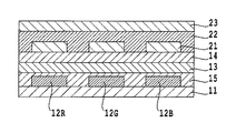
本発明の有機EL発光ディスプレイの1つの構成例を図1に示す。図1は、透明基板11の上に、3種のカラーフィルタ層12(R,G,B)、色変換層13、バリア層14および有機EL素子が形成された色変換方式の有機EL発光ディスプレイを示す。ここで、有機EL素子は、透明電極21、有機EL層22および反射電極23から構成されている。また、3種のカラーフィルタ層12(R,G,B)はウェットプロセスで形成され、一方、色変換層13はドライプロセスで形成される。
One structural example of the organic EL light emitting display of the present invention is shown in FIG. FIG. 1 shows a color conversion type organic EL light emitting display in which three kinds of color filter layers 12 (R, G, B), a
本発明の有機EL発光ディスプレイの別の構成例を図2に示す。図2の構成は、カラーフィルター層12を覆うオーバーコート層15が設けられている点を除いて、図1の構成と同様である。以下に、本発明の有機EL発光ディスプレイを構成する層のそれぞれについて詳細を述べる。
FIG. 2 shows another configuration example of the organic EL light emitting display of the present invention. The configuration of FIG. 2 is the same as the configuration of FIG. 1 except that an
透明基板11は可視光透過率に優れ、また、有機EL発光ディスプレイの形成プロセスにおいて、有機EL発光ディスプレイの性能低下を引き起こさないものであれば良い。好ましい透明基板は、ガラス基板、およびポリオレフィン、アクリル樹脂(ポリメチルメタクリレートを含む)、ポリエステル樹脂(ポリエチレンテレフタレートを含む)、ポリカーボネート樹脂、またはポリイミド樹脂などの樹脂で形成された剛直性の樹脂基板を含む。あるいはまた、ポリオレフィン、アクリル樹脂(ポリメチルメタクリレートを含む)、ポリエステル樹脂(ポリエチレンテレフタレートを含む)、ポリカーボネート樹脂、またはポリイミド樹脂などから形成される可撓性フィルムを、基板として用いてもよい。ガラス、ならびにポリエチレンテレフタレート、ポリメチルメタクリレート等の樹脂を含む。ホウケイ酸ガラスまたは青板ガラス等が特に好ましいものである。
The
本発明におけるカラーフィルター層12は、入射光を分光して、所望される波長域の光のみを透過させる層である。図1の構成では赤色カラーフィルター層12R、緑色カラーフィルター層12Gおよび青色カラーフィルター層12Bの3種のカラーフィルター層を用いているが、必要に応じて1種、2種、または4種以上のカラーフィルター層を用いてもよい。カラーフィルター層12は、所望の吸収を有する染料または顔料を高分子のマトリクス樹脂中に分散させたものであり、市販のフラットパネルディスプレイ用材料などの当該技術において知られている任意の材料、たとえば液晶用カラーフィルター材料(富士フィルムエレクトロニクスマテリアルズ(株)製カラーモザイクなど)を用いて形成することができる。本発明におけるカラーフィルター層12は、所望される波長域の光を高い色純度で得るために、0.5〜5μm、好ましくは1〜3μm、より好ましくは1〜1.5μmの膜厚を有する。
The color filter layer 12 in the present invention is a layer that splits incident light and transmits only light in a desired wavelength region. In the configuration of FIG. 1, three types of color filter layers, a red
図1および図2には例示していないが、各カラーフィルター層12の間隙に、光を透過させないブラックマトリクスを形成してもよい。ブラックマトリクスは、カラーフィルター層12と同様に、市販のフラットパネルディスプレイ用材料などの当該技術において知られている任意の材料を用いて形成することができる。ブラックマトリクスは、有機EL発光ディスプレイのコントラスト比を向上させることに有効である。ここで、ブラックマトリクスの一部とカラーフィルター層12の一部とを重畳(オーバーラップ)させて、有機EL素子からの光が必ずカラーフィルター層12を通過して出射するようにしてもよい。 Although not illustrated in FIGS. 1 and 2, a black matrix that does not transmit light may be formed in the gaps between the color filter layers 12. Similarly to the color filter layer 12, the black matrix can be formed using any material known in the art such as a commercially available flat panel display material. The black matrix is effective in improving the contrast ratio of the organic EL light emitting display. Here, a part of the black matrix and a part of the color filter layer 12 may be superposed (overlapped) so that the light from the organic EL element always passes through the color filter layer 12 and is emitted.
また、図2に示すように、カラーフィルター層12(および、存在する場合にはブラックマトリクス)を覆うオーバーコート層15を設けてもよい。オーバーコート層15は、カラーフィルター層12によってもたらされる段差を補償するための層である。本発明のカラーフィルター層12は、ウェットプロセスで形成される従来型の色変換層よりも著しく薄いので、それによってもたらされる段差もまた小さい。したがって、カラーフィルター層12の段差はより容易に補償することが可能である。また、有機EL素子からの光がオーバーコート層15を通って外部へと放射することから、オーバーコート層15の材料は優れた光透過性を有すること(波長400〜800nmの光に対して好ましくは50%以上、より好ましくは85%以上の透過率を有すること)が望ましい。オーバーコート層15を形成するための材料としては、熱可塑性樹脂(アクリル樹脂(メタクリル樹脂を含む))、ポリエステル樹脂(ポリエチレンテレフタレートなど)、ポリアミド樹脂、ポリイミド樹脂、ポリエーテルイミド樹脂、ポリアセタール樹脂、ポリエーテルサルホン、ポリビニルアルコールおよびその誘導体(ポリビニルブチラールなど)、ポリフェニレンエーテル、ノルボルネン系樹脂、イソブチレン無水マレイン酸共重合樹脂、環状オレフィン系樹脂)、非感光性の熱硬化型樹脂(アルキッド樹脂、芳香族スルホンアミド樹脂、ユリア樹脂、メラミン樹脂、ベンゾグアナミン樹脂)、または光硬化型樹脂を用いることができる。
Further, as shown in FIG. 2, an
オーバーコート層15は、カラーフィルター層12とオーバーラップしていない領域において0.5〜3μm、より好ましくは1〜2μmの膜厚を有して、複数種のカラーフィルター層12によってもたらされる段差を補償し、平坦な上平面を提供することができる。
The
色変換層13は、入射光(有機EL素子からの発光)の一部を吸収して異なる波長の光を放射し、入射光の非吸収分と変換光とを含む異なる波長分布を有する光を得るための層である。好ましくは、色変換層13は、有機EL素子からの青色〜青緑色光を、白色光に変換する。本発明における白色光とは、可視領域(400〜700nm)の波長成分を均一に含む光のみならず、該波長成分を均一には含んでいないが肉眼で白色に見える光をも含む。色変換色素は、入射光を吸収して、異なる波長域の光を放射する色素であり、好ましくは光源が発する青色〜青緑色の光を吸収して、所望の波長域の光(たとえば、緑色または赤色)を放射する色素である。色変換色素としては、DCM−1(I)、DCM−2(II)、DCJTB(III)、4,4−ジフルオロ−1,3,5,7−テトラフェニル−4−ボラ−3a,4a−ジアザ−s−インダセン(IV)、ナイルレッド(V)などの赤色発光材料用の色素;赤色光を放射するローダミン系色素、シアニン系色素、ピリジン系色素、オキサジン系色素など:緑色光を放射するクマリン系色素、ナフタルイミド系色素など、当該技術で知られている任意のものを用いることができる。
The

本発明の色変換層13は、色変換色素に加えて、ホスト材料をさらに含んでもよい。色変換色素をホスト材料中に分散させることによって、濃度消光による色変換効率の低下を抑制することができる。加えて、ホスト材料として、発光層からの発光を吸収して色変換色素にエネルギーを移動させることが可能な材料を用いることによって、色変換の効率を向上させることもできる。ホスト材料として蒸着可能な低分子材料を用いて、色変換色素とホスト材料とを共蒸着させることが望ましい。本発明において用いることができるホスト材料としては、たとえば、トリス(8−ヒドロキシキノリナト)アルミニウム(Alq3)またはトリス(4−メチル−8−ヒドロキシキノリナト)アルミニウム(Almq3)のようなアルミニウム錯体、4,4’−ビス(2,2−ジフェニルビニル)ビフェニル(DPVBi)、2,5−ビス−(5−tert−ブチル−2−ベンゾオキサゾリル)チオフェンなどの材料を挙げることができる。
The
色変換層13は、100nm〜2μm、好ましくは150nm〜500nmの範囲内の膜厚を有して、ディスプレイ全面にわたって形成される。したがって、本発明の色変換層13は、色変換色素/マトリクス樹脂の組成物の塗布・乾燥によって形成される従来型の色変換層とは異なり、透明電極21および反射電極23の断線または短絡などの故障を引き起こすような段差を形成することはない。したがって、色変換層13の上に平坦化のための層を設ける必要性が排除される。
The
また、色変換色素/マトリクス樹脂の組成物の塗布・乾燥によって形成される従来型の色変換層においては、その層中に有機EL素子の劣化を引き起こす水分を包含する恐れがある。しかしながら、本発明の色変換層はドライプロセスである蒸着法を用いて形成されるのでそのような水分を包含する恐れがなく、したがって有機EL素子の劣化の原因となることもない。 Further, in a conventional color conversion layer formed by applying and drying a composition of a color conversion dye / matrix resin, there is a possibility that the layer contains moisture that causes deterioration of the organic EL element. However, since the color conversion layer of the present invention is formed by using a vapor deposition method which is a dry process, there is no fear of including such moisture, and therefore it does not cause deterioration of the organic EL element.
任意選択的に、色変換層13の直下に、SiO2、SiNなどのケイ素化合物、あるいはAl2O3のようなアルミニウム化合物を用いて下地層(不図示)を形成してもよい。下地層は、色変換層13の密着性を向上させるために有効な層であり、水分、酸素および低分子成分に対するバリア性を付与する目的においても有効である。形成される場合、下地層は、50nm〜2μm、より好ましくは100nm〜200nmの範囲内の膜厚を有することが望ましい。
Optionally, a base layer (not shown) may be formed immediately below the
バリア層14は、その上に形成される有機EL素子の透明電極21の形成プロセスから色変換層13を保護するための層である。したがって、バリア層14は、水分に対するバリア性を有する材料で形成される。さらに、バリア層14は、有機EL層22の発光を色変換層13側に効率よく透過させるために、その発光波長域において透明であること(400〜800nmの範囲で50%以上の高い透過率を有すること)が望ましい。バリア層14として好適な材料は、SiN、AlNなどを含む。バリア層14は、100nm〜2μm、より好ましくは200nm〜1μmの範囲内の膜厚を有して、色変換層13上の全面にわたって形成される。
The
本発明に使用することができる有機EL発光素子は、透明電極21、有機EL層22、および反射電極23がこの順に積層した構造を有する。有機EL層22は、少なくとも有機発光層を含み、必要に応じて正孔注入層、正孔輸送層、電子輸送層および/または電子注入層を介在させた構造を有している。あるいはまた、正孔の注入および輸送の両方の機能を有する正孔注入輸送層、電子の注入および輸送の両方の機能を有する電子注入輸送層を用いてもよい。具体的には、有機EL素子は下記のような層構造からなるものが採用される。
(1)陽極/有機発光層/陰極
(2)陽極/正孔注入層/有機発光層/陰極
(3)陽極/有機発光層/電子注入層/陰極
(4)陽極/正孔注入層/有機発光層/電子注入層/陰極
(5)陽極/正孔輸送層/有機発光層/電子注入層/陰極
(6)陽極/正孔注入層/正孔輸送層/有機発光層/電子注入層/陰極
(7)陽極/正孔注入層/正孔輸送層/有機発光層/電子輸送層/電子注入層/陰極
上記の層構成において、陽極および陰極は、それぞれ透明電極21または反射電極23のいずれかである。当該技術において、陽極を透明にすることが容易であることが知られており、本発明においても透明電極21を陽極として、および反射電極23を陰極として用いることが望ましい。透明電極21は、有機EL層22の発する光の波長域において透明であることが望ましい。
The organic EL light-emitting element that can be used in the present invention has a structure in which a
(1) Anode / organic light emitting layer / cathode (2) Anode / hole injection layer / organic light emitting layer / cathode (3) Anode / organic light emitting layer / electron injection layer / cathode (4) Anode / hole injection layer / organic Light emitting layer / electron injection layer / cathode (5) Anode / hole transport layer / organic light emitting layer / electron injection layer / cathode (6) Anode / hole injection layer / hole transport layer / organic light emitting layer / electron injection layer / Cathode (7) Anode / hole injection layer / hole transport layer / organic light emitting layer / electron transport layer / electron injection layer / cathode In the above layer configuration, the anode and the cathode are either
有機EL層22を構成する各層の材料としては、公知のものが使用される。例えば、有機発光層として青色から青緑色の発光を得るためには、例えばベンゾチアゾール系、ベンゾイミダゾール系、ベンゾオキサゾール系などの蛍光増白剤、金属キレート化オキソニウム化合物、スチリルベンゼン系化合物、芳香族ジメチリディン系化合物などが好ましく使用される。
As the material of each layer constituting the
透明電極21は、波長400〜800nmの光に対して好ましくは50%以上、より好ましくは85%以上の透過率を有することが好ましい。透明電極21は、ITO(In−Sn酸化物)、Sn酸化物、In酸化物、IZO(In−Zn酸化物)、Zn酸化物、Zn−Al酸化物、Zn−Ga酸化物、またはこれらの酸化物に対してF、Sbなどのドーパントを添加した導電性透明金属酸化物を用いて形成することができる。透明電極21を陰極として用いる場合、有機EL層22との界面にバッファ層を設けて、電子注入効率を向上させることが望ましい。バッファ層の材料としては、Li、Na、K、またはCsなどのアルカリ金属、Ba、Srなどのアルカリ土類金属またはそれらを含む合金、希土類金属、あるいはそれら金属のフッ化物などを用いることができるが、それらに限定されるものではない。バッファ層の膜厚は、駆動電圧および透明性等を考慮して適宜選択することができるが、通常の場合には10nm以下であることが好ましい。
The
反射電極23は、高反射率の金属、アモルファス合金、微結晶性合金を用いて形成されることが好ましい。高反射率の金属は、Al、Ag、Mo、W、Ni、Crなどを含む。高反射率のアモルファス合金は、NiP、NiB、CrPおよびCrBなどを含む。高反射率の微結晶性合金は、NiAlなどを含む。反射電極23を、陰極として用いてもよいし、陽極として用いてもよい。反射電極23を陰極として用いる場合には、反射電極23と有機EL層22との界面に、前述のバッファ層を設けて有機EL層22に対する電子注入の効率を向上させてもよい。あるいはまた、反射電極23を陰極として用いる場合、前述の高反射率金属、アモルファス合金または微結晶性合金に対して、仕事関数が小さい材料であるリチウム、ナトリウム、カリウム等のアルカリ金属、カルシウム、マグネシウム、ストロンチウムなどのアルカリ土類金属を添加して合金化し、電子注入効率を向上させることができる。反射電極23を陽極として用いる場合には、反射電極23と有機EL層22との界面に、前述の導電性透明金属酸化物の層を設けて有機EL層22に対する正孔注入の効率を向上させてもよい。
The
図1および図2の構成において、有機EL素子中に複数の独立した発光部を形成するために、透明電極21および反射電極23のそれぞれは平行なストライプ状の複数の部分から形成され、透明電極21を形成するストライプと反射電極23を形成するストライプとが互いに交差(好ましくは直交)するように形成されている。したがって、有機EL発光素子はマトリクス駆動を行うことができ、すなわち、透明電極21の特定のストライプと、反射電極23の特定のストライプに電圧が印加された時に、それらのストライプが交差する部分において有機EL層22が発光する。あるいはまた、一方の電極(たとえば、透明電極21)をストライプパターンを持たない一様な平面電極とし、および他方の電極(たとえば、反射電極23)を各発光部に対応するような複数の部分電極にパターニングしてもよい。その場合には、各発光部に対応する複数のスイッチング素子を設けて各発光部に対応する前記の部分電極に1対1で接続して、いわゆるアクティブマトリクス駆動を行うことが可能になる。
1 and 2, in order to form a plurality of independent light emitting portions in the organic EL element, each of the
次いで、本発明の有機EL発光ディスプレイの製造方法について述べる。最初に透明基板11の上に、液体状材料(溶液または分散液)の塗布、光パターニング、現像液による不要部分の除去を含むウェットプロセスによるフォトリソグラフィー法を用いて、カラーフィルター層12を形成する。必要な精細度を簡便に得る方法として、ウェットプロセスの適用が好ましい。複数種のカラーフィルター層12を用いる場合には、所望の回数にわたってウェットプロセスを繰り返すことができる。
Next, a method for manufacturing the organic EL light emitting display of the present invention will be described. First, the color filter layer 12 is formed on the
任意選択的にカラーフィルター層12の間隙にブラックマトリクスを設ける場合には、ブラックマトリクスを先に形成してもよいし、カラーフィルター層12を先に形成してもよい。ブラックマトリクスは、カラーフィルター層12と同様のウェットプロセスを用いて形成することができる。 When the black matrix is optionally provided in the gap between the color filter layers 12, the black matrix may be formed first, or the color filter layer 12 may be formed first. The black matrix can be formed using a wet process similar to that of the color filter layer 12.
さらに任意選択的に、カラーフィルター層12を覆うオーバーコート層15を設ける場合には、一般的に、前述の材料の溶液または分散液を、スピンコート、ロールコート、ナイフコートなどの塗布法によって付着させ、次いで乾燥させることによって、オーバーコート層15を形成する。
Further optionally, when an
カラーフィルター層12、ならびにブラックマトリクスおよびオーバーコート層15(存在する場合)の形成終了後に、その積層物を高温加熱して、カラーフィルター層12、ブラックマトリクス、オーバーコート層15中に残存する水分を十分に除去する。この工程は、積層物を乾燥雰囲気(水分濃度1ppm以下)に配置し、引き続いて15〜60分間にわたって、200〜250℃に加熱することによって実施される。本工程は、大気圧下で行ってもよいし、減圧下(好ましくは0.13〜13.3kPa(1〜100mmHg)程度の圧力)で行ってもよい。加熱終了後、乾燥雰囲気を維持したままで積層物を次の成膜を行う装置へと移送する。このときに、必要に応じて、積層物を冷却してもよい。
After the formation of the color filter layer 12 and the black matrix and overcoat layer 15 (if present), the laminate is heated to a high temperature to remove moisture remaining in the color filter layer 12, black matrix, and
色変換層13の直下に下地層を形成する場合には、積層物を適切な成膜装置へと移送する。繰り返しになるが、この段階の移送は乾燥雰囲気下で実施される。そして、蒸着法(抵抗加熱方式、電子ビーム加熱方式を含む)、スパッタ法(高周波スパッタ、マグネトロンスパッタを含む)、またはCVD法などを用いて、積層物上に下地層を積層する。積層終了後、乾燥雰囲気を維持したまま、積層物を色変換層成膜用の蒸着装置へと移送する。移送は、減圧を破ることなしに行ってもよいし、一旦減圧を解除してもよいが、乾燥雰囲気を維持して行うべきである。
When forming a base layer directly under the
次いで、1種または複数種の色変換色素、および任意選択的に共蒸着材料を蒸着して、色変換層13を形成する。本発明においては、抵抗加熱蒸着を行ってもよいし、電子ビーム加熱蒸着を行ってもよい。また、複数種の蒸着源を用いる場合には、それらを予め混合した混合物を加熱してもよく、それぞれの蒸着源を別個に加熱して蒸着膜の組成を制御できるようにしてもよい。色変換層13の形成終了後、積層物をCVD装置へと移送する。移送は、減圧を破ることなしに行ってもよいし、一旦減圧を解除してもよいが、乾燥雰囲気を維持して行うべきである。
Next, one or a plurality of color conversion dyes and optionally a co-evaporation material are vapor-deposited to form the
次に、バリア層14を形成する。本発明においては、ピンホールのない緻密な膜を低温かつ高い成膜速度で形成する手段としてCVD法を用いてバリア層14を形成することが好ましい。プラズマCVD法を用いることがより好ましい。なぜなら、熱CVD法では、反応温度として1000℃近い高温が必要であり、カラーフィルター層12または色変換層13中の有機物が焼尽してしまうため、適用が難しいからである。一方、プラズマCVD法においては、プラズマ中で原料ガスの電離・反応を行うために高温を必要としない。さらに、プラズマの発生手段としては、高周波電力(容量結合型または誘導結合型のいずれであってもよい)、ECR、ヘリコン波などの当該技術で知られている任意の手段を用いてもよい。また、高周波電力として、HF領域の工業用周波数(13.56MHz)の電力に加えて、MF、UHFまたはVHF領域の周波数の電力を用いることも可能である。異なる周波数を有する2つ以上の高周波電力を使用してもよい。
Next, the
本工程における原料ガスとしては、SiH4、SiH2Cl2、SiCl4、Si(OC2H5)4などのSi源、AlCl3、Al(O−i−C3H7)3、有機アルミニウム化合物(トリメチルアルミニウム、トリエチルアルミニウム、トリブチルアルミニウムなど)などのAl源、および/またはNH3などのN源を用いることができる。これらの原料ガスに加えて、CVD装置中にH2、N2あるいは不活性ガス(He、Arなど)を希釈ガスとして導入してもよい。 As source gases in this step, Si sources such as SiH 4 , SiH 2 Cl 2 , SiCl 4 , Si (OC 2 H 5 ) 4 , AlCl 3 , Al (OiC 3 H 7 ) 3 , organic aluminum compound (trimethylaluminum, triethylaluminum, tri-butyl aluminum, etc.) can be used Al source, and / or N sources such as NH 3 and the like. In addition to these source gases, H 2 , N 2 or an inert gas (He, Ar, etc.) may be introduced as a dilution gas into the CVD apparatus.
たとえば、バリア層14としてSiN膜を形成する場合、原料ガスとしてSiH4とNH3を用い、SiH4:NH3の分圧の比を1:10〜5:10とし、全圧力を50〜150Paとすることができる。そのような条件を用いることによって、ピンホールが少なく、かつ内部応力が小さい良質のSiN膜を得ることができる。
For example, when a SiN film is formed as the
本発明においては、カラーフィルター層12などの加熱乾燥工程から、バリア層14の形成工程に至るまでの間、積層物を湿潤環境(大気など)に曝さないことが重要である。このことによって、加熱乾燥したカラーフィルター層12などへの水分の再吸着を防止することが可能となる。また、この間の工程においてドライプロセスによって有機物から形成される色変換層13は、ほぼ無水の状態であり、水分を非常に吸着しやすい状態にある。したがって、色変換層13への水分の吸着を防止する点からも、乾燥雰囲気の維持は重要である。そのようにバリア層14以下の層を完全に無水にすることによって、ピンホールのない緻密なバリア層14を成膜することが可能となる。
In the present invention, it is important that the laminate is not exposed to a moist environment (such as the atmosphere) from the heat drying step of the color filter layer 12 and the like to the step of forming the
次いで、有機EL素子の作製を行う。最初に、蒸着法、スパッタ法または化学気相堆積(CVD)法を用いて導電性透明金属酸化物を堆積することによって、透明電極21を形成する。好ましくは、透明電極21はスパッタ法を用いて形成される。ここで、前述のように複数の部分電極からなる透明電極21が必要になる場合、全面にわたって導電性透明金属酸化物膜を均一に積層し、その後にパターニングを行ってもよい。パターニングは、フォトリソグラフ法を含むウェットプロセスであってもよい。
Next, an organic EL element is manufactured. First, the
ここで、後述する反射電極23が複数のストライプ形状の部分電極から形成される場合、透明電極21の上に、反射電極分離隔壁を設けてもよい。反射電極分離隔壁は、逆テーパー形状の断面を有する複数のストライプ形状の部分から構成される。この逆テーパー形状は、フォトレジストを用い、ベークおよび露光の条件を制御することによって実現することができる。
Here, when a
以上のように、透明電極21のパターニング、または反射電極分離隔壁の形成の際に、バリア層14は湿潤環境にさらされる可能性がある。しかしながら、本発明においては、完全な状態のバリア層14が得られるので、バリア層14の下にある色変換層13が湿潤環境にさらされる可能性はない。したがって、色変換層13の部分剥離および色変換効率の低下を防止することができる。
As described above, when patterning the
次に、透明電極21を覆うように有機EL層22を積層する。有機EL層22を構成する各層を、蒸着法を用いて形成することが望ましい。
Next, the
最後に、有機EL層22の上に、蒸着法を用いて反射電極23を積層する。複数の部分電極(たとえば、複数のストライプ形状の部分電極)からなる反射電極23を形成する場合には、前述のように設けられた反射電極分離隔壁を用いて複数のストライプ形状の部分電極への分離を行ってもよい。あるいはまた、蒸着時に所望の形状を与えるマスクを用いて、複数の部分電極からなる反射電極23を形成してもよい。
Finally, the
以上に述べた有機EL素子の作製においては、透明電極21のパターニングおよび反射電極分離隔壁の形成(使用する場合)の際にウェットプロセスを用いており、その時点で積層物は湿潤雰囲気にさらされる。しかしながら、有機EL素子の作製を、乾燥雰囲気を破ることなしに実施することもできる。この場合には、複数の部分電極からなる透明電極21の積層を、所望の形状を与えるマスクを用いて実施する。ここで、スパッタ法を用いて透明電極21を積層する場合には、ターゲット−被堆積基板間の距離の増大、コリメータ板の挿入などのような成膜粒子の飛翔方向を揃える手段を併用することが望ましい。その後に、反射電極分離隔壁を作製することなしに、有機EL層22を蒸着法により形成する。最後に、所望の形状を与えるマスクを用いる蒸着法にて、複数の部分電極からなる反射電極23を形成して、有機EL発光ディスプレイを得る。
In the production of the organic EL element described above, a wet process is used for patterning the
この方法を採用した場合、色変換層13に加えて、バリア層14の一部(透明電極21に覆われない部分)および透明電極21も湿潤環境にさらすことなしに、有機EL発光ディスプレイを製造することが可能となり、ダークエリアの発生がない安定な有機EL発光ディスプレイを与えることができる。
When this method is adopted, an organic EL light-emitting display is manufactured without exposing part of the barrier layer 14 (the portion not covered by the transparent electrode 21) and the
[実施例1]
厚さ0.7mmのガラス基板11を純水中で超音波洗浄し、乾燥させた後に、さらにUVオゾン洗浄した。洗浄済ガラス基板に対して、スピンコート法を用いてカラーモザイクCK−7800(富士フィルムエレクトロニクスマテリアルズ(株)製)を塗布し、フォトリソグラフ法を用いてパターニングを行い、幅0.09mm×長さ0.3mmを有する複数の開口部が、幅方向ピッチ0.11mmおよび幅方向ピッチ0.33mmで配列されている膜厚1μmのブラックマトリクスを形成した。
[Example 1]
The
引き続いて、赤色、緑色および青色の各カラーフィルター層を、それぞれ、カラーモザイクCR−7001、CG−7001、およびCB−7001を用いて形成した。それぞれのカラーフィルター層材料を塗布した後に、フォトリソグラフ法を用いてパターニングして幅0.10mm、膜厚1μm(ガラス基板11上)の複数のストライプ状部分がピッチ0.33mmで配列されている赤色カラーフィルター層12R、緑色カラーフィルター層12G、および青色カラーフィルター層12Bを形成した。この構造において、各カラーフィルター層の複数のストライプ状部分のそれぞれは、その側辺から0.005mmの領域において、ブラックマトリクスにオーバーラップした。
Subsequently, red, green, and blue color filter layers were formed using color mosaics CR-7001, CG-7001, and CB-7001, respectively. After applying each color filter layer material, patterning is performed using a photolithographic method, and a plurality of stripe portions having a width of 0.10 mm and a film thickness of 1 μm (on the glass substrate 11) are arranged at a pitch of 0.33 mm. A red
次に、NN810L(JSR製)をスピンコート法によって塗布および露光して、カラーフィルター層12およびブラックマトリクスを覆うオーバーコート層15を形成した。ブラックマトリクスと接触する領域におけるオーバーコート層15の膜厚は1.5μmであった。
Next, NN810L (manufactured by JSR) was applied and exposed by a spin coating method to form an
以上のように得られたオーバーコート層15以下の層を有する基板を、乾燥窒素雰囲気(水分濃度1ppm以下)下、60分間にわたって220℃に加熱して、残存する可能性のある水分を除去した。
The substrate having the
次いで、乾燥窒素雰囲気を維持したまま、オーバーコート層15を形成した基板を真空蒸着装置に装着し、1×10⁻⁴Paの圧力において、0.3Å/sの蒸着速度にてDCM−1を蒸着し、膜厚500nmの色変換層13を形成した。
Next, while maintaining the dry nitrogen atmosphere, the substrate on which the
そして、乾燥窒素を用いて圧力を大気圧に戻した後に、乾燥窒素雰囲気を維持しつつ、色変換層13を形成した基板を蒸着装置からCVD装置に移送した。該装置内で、プラズマCVD法を用いて膜厚300nmのSiN膜を積層して、バリア層14を得た。原料ガスとして100SCCMのSiH4、500SCCMのNH3、および3000SCCMのN2を用い、ガス圧を100Paとした。また、プラズマ発生用電力として、13.56MHzのRF電力を500W、および400kHzのRF電力を40W印加した。
And after returning pressure to atmospheric pressure using dry nitrogen, the board | substrate with which the
以上のように形成したバリア層14の上に、有機EL素子を形成する。最初に、DCスパッタ法を用いて膜厚200nmのIZO膜を成膜した。ターゲットとしてIn−Zn酸化物を用い、スパッタガスとしてO2およびArを用いた。次いで、シュウ酸水溶液をエッチング液として用いるフォトリソグラフ法によってパターニングを行い、透明電極21を得た。透明電極21は、カラーフィルター層12の上方に位置し、カラーフィルター層12のストライプと同一方向に伸びる複数のストライプ状部分(幅0.1mm、ピッチ0.11mm)から形成された。
An organic EL element is formed on the
次いで、フォトニース(東レ株式会社製)を用いてポリイミド膜を形成し、フォトリソグラフ法を用いて、幅0.09mm×長さ0.3mmを有する複数の開口部(有機EL素子の発光部となる部分)が、幅方向ピッチ0.11mmおよび幅方向ピッチ0.33mmで配列されている絶縁膜を形成した。この際に、絶縁膜の開口部がブラックマトリクスの開口部に対応して位置するようにした。引き続いて、反射電極分離隔壁の形成を行った。ネガ型フォトレジスト(ZPN1168(日本ゼオン製))をスピンコート法によって塗布し、プリベークを実施し、フォトマスクを用いて透明電極21のストライプと直交する方向に伸びるストライプ形状のパターンを焼き付け、110℃のホットプレート上で60秒間にわたってポストエクスポージャベークを行い、現像を行い、最後に180℃のホットプレート上で15分間にわたって加熱を行い、反射電極分離隔壁を形成した。得られた反射電極分離隔壁は、逆テーパー形状の断面を有し、透明電極21のストライプと直交する方向に伸びる複数のストライプ形状部から構成された。
Next, a polyimide film is formed using Photonice (manufactured by Toray Industries, Inc.), and a plurality of openings having a width of 0.09 mm × a length of 0.3 mm (a light emitting portion of an organic EL element and a photolithographic method) are used. The insulating film in which the portion is formed with a width direction pitch of 0.11 mm and a width direction pitch of 0.33 mm is formed. At this time, the opening of the insulating film was positioned corresponding to the opening of the black matrix. Subsequently, a reflective electrode separation partition was formed. A negative photoresist (ZPN1168 (manufactured by ZEON Corporation)) is applied by spin coating, pre-baked, and a stripe-shaped pattern extending in a direction perpendicular to the stripes of the
以上のように反射電極分離隔壁を形成した基板を抵抗加熱蒸着装置内に装着し、正孔注入層、正孔輸送層、有機発光層および電子注入層からなる有機EL層22を、真空を破らずに順次成膜した。成膜に際して真空槽内圧は1×10⁻⁴Paまで減圧した。正孔注入層として膜厚100nmの銅フタロシアニン(CuPc)、正孔輸送層として膜厚20nmの4,4’−ビス[N−(1−ナフチル)−N−フェニルアミノ]ビフェニル(α−NPD)、発光層として膜厚30nmのDPVBi、および電子注入層として膜厚20nmのAlq3を積層して、有機EL層22を得た。
As described above, the substrate on which the reflective electrode separation barrier rib is formed is mounted in a resistance heating vapor deposition apparatus, and the
この後、真空を破ることなしに、厚さ200nmのMg/Ag(10:1の質量比)膜を堆積させ、幅0.30mm、ピッチ0.33mmの複数のストライプ形状の部分電極からなる反射電極23を得た。
Thereafter, without breaking the vacuum, a 200 nm thick Mg / Ag (10: 1 mass ratio) film is deposited, and the reflection is made of a plurality of stripe-shaped partial electrodes having a width of 0.30 mm and a pitch of 0.33 mm. An
こうして得られたデバイスをグローブボックス内乾燥窒素雰囲気(水分濃度1ppm以下)下において、封止ガラスとUV硬化接着剤を用いて封止して、有機EL発光ディスプレイを得た。得られたディスプレイを、輝度1000cd/m2で白色(初期色度(CIE)、x=0.31、y=0.33)発光する条件にて、85℃において1000時間にわたって連続駆動したが、ダークエリアの発生は観測されなかった。 The device thus obtained was sealed using a sealing glass and a UV curable adhesive in a dry nitrogen atmosphere (moisture concentration of 1 ppm or less) in the glove box to obtain an organic EL light emitting display. The obtained display was continuously driven at 85 ° C. for 1000 hours under the condition of emitting white light (initial chromaticity (CIE), x = 0.31, y = 0.33) at a luminance of 1000 cd / m 2 . No dark area was observed.
[比較例1]
色変換層13の形成後、10分間にわたって湿潤環境(30%RHの大気中)に基板をさらしたことを除いて実施例1と同様の手順を繰り返して、有機EL発光ディスプレイを得た。得られたディスプレイを、輝度1000cd/m2で白色(初期色度(CIE)、x=0.31、y=0.33)発光する条件にて、85℃において1000時間にわたって連続駆動したところ、1cm2あたり数個のダークエリアが発生した。
[Comparative Example 1]
After the
11,31 透明基板
12,32(R、G、B) カラーフィルター層
13 色変換層
14 バリア層
15 オーバーコート層
21、41 透明電極
22、42 有機EL層
23,43 反射電極
33(R、G、B) (従来型)色変換層
34 平坦化層
35 ガスバリア層
11, 31 Transparent substrate 12, 32 (R, G, B)
Claims (4)
該透明基板を加熱乾燥する工程と、
前記カラーフィルター層の上に色変換層を形成する工程と、
該色変換層の上にバリア層を形成する工程と、
該バリア層の上に有機EL素子を形成する工程と
を含み、前記加熱乾燥工程から前記バリア層形成工程までを1ppm以下の水分濃度を有する乾燥雰囲気下で実施することを特徴とする有機EL発光ディスプレイの製造方法。 Forming one or more color filter layers on a transparent substrate by a wet process;
Heating and drying the transparent substrate;
Forming a color conversion layer on the color filter layer;
Forming a barrier layer on the color conversion layer;
Forming an organic EL element on the barrier layer, and performing from the heat drying step to the barrier layer forming step in a dry atmosphere having a moisture concentration of 1 ppm or less. Display manufacturing method.
Priority Applications (1)
| Application Number | Priority Date | Filing Date | Title |
|---|---|---|---|
| JP2005299157A JP4674524B2 (en) | 2005-10-13 | 2005-10-13 | Manufacturing method of organic EL light emitting display |
Applications Claiming Priority (1)
| Application Number | Priority Date | Filing Date | Title |
|---|---|---|---|
| JP2005299157A JP4674524B2 (en) | 2005-10-13 | 2005-10-13 | Manufacturing method of organic EL light emitting display |
Publications (2)
| Publication Number | Publication Date |
|---|---|
| JP2007109518A JP2007109518A (en) | 2007-04-26 |
| JP4674524B2 true JP4674524B2 (en) | 2011-04-20 |
Family
ID=38035231
Family Applications (1)
| Application Number | Title | Priority Date | Filing Date |
|---|---|---|---|
| JP2005299157A Active JP4674524B2 (en) | 2005-10-13 | 2005-10-13 | Manufacturing method of organic EL light emitting display |
Country Status (1)
| Country | Link |
|---|---|
| JP (1) | JP4674524B2 (en) |
Families Citing this family (7)
| Publication number | Priority date | Publication date | Assignee | Title |
|---|---|---|---|---|
| DE102007053069A1 (en) | 2007-09-27 | 2009-04-02 | Osram Opto Semiconductors Gmbh | Light-emitting component with wavelength converter and manufacturing method |
| JP5069581B2 (en) * | 2008-02-01 | 2012-11-07 | 富士フイルム株式会社 | Method for forming gas barrier film, gas barrier film, and organic EL element |
| JP5139894B2 (en) * | 2008-06-20 | 2013-02-06 | 富士フイルム株式会社 | Method for forming gas barrier film and gas barrier film |
| JP5405075B2 (en) * | 2008-09-24 | 2014-02-05 | 富士フイルム株式会社 | Method for forming gas barrier film and gas barrier film |
| JP2015026417A (en) * | 2011-11-18 | 2015-02-05 | シャープ株式会社 | Organic electroluminescent display device and electronic apparatus using the same, and method for manufacturing organic electroluminescent display device |
| JP2015026418A (en) * | 2011-11-18 | 2015-02-05 | シャープ株式会社 | Organic electroluminescent display device and electronic apparatus using the same, and method for manufacturing organic electroluminescent display device |
| DE102014100837A1 (en) * | 2014-01-24 | 2015-07-30 | Osram Opto Semiconductors Gmbh | Light-emitting component and method for producing a light-emitting component |
Citations (3)
| Publication number | Priority date | Publication date | Assignee | Title |
|---|---|---|---|---|
| JP2002075643A (en) * | 2000-08-29 | 2002-03-15 | Tdk Corp | Organic el display panel and organic el device used therein |
| JP2002175879A (en) * | 2000-12-08 | 2002-06-21 | Tdk Corp | Organic el display panel and organic el element using the same |
| JP2002184575A (en) * | 2000-12-11 | 2002-06-28 | Tdk Corp | Organic el display device |
-
2005
- 2005-10-13 JP JP2005299157A patent/JP4674524B2/en active Active
Patent Citations (3)
| Publication number | Priority date | Publication date | Assignee | Title |
|---|---|---|---|---|
| JP2002075643A (en) * | 2000-08-29 | 2002-03-15 | Tdk Corp | Organic el display panel and organic el device used therein |
| JP2002175879A (en) * | 2000-12-08 | 2002-06-21 | Tdk Corp | Organic el display panel and organic el element using the same |
| JP2002184575A (en) * | 2000-12-11 | 2002-06-28 | Tdk Corp | Organic el display device |
Also Published As
| Publication number | Publication date |
|---|---|
| JP2007109518A (en) | 2007-04-26 |
Similar Documents
| Publication | Publication Date | Title |
|---|---|---|
| CN101305643B (en) | Organic el light emitting display | |
| US6013538A (en) | Method of fabricating and patterning OLEDs | |
| JP5236732B2 (en) | Color conversion film and multicolor light emitting organic EL device including the color conversion film | |
| JP4674524B2 (en) | Manufacturing method of organic EL light emitting display | |
| US8183564B2 (en) | Multicolor display apparatus | |
| WO1998034437A1 (en) | Organic electroluminescent display device | |
| JP2010517207A (en) | Color conversion layer patterning method and organic EL display manufacturing method using the same | |
| JP2008226718A (en) | Organic el device | |
| WO2009098793A1 (en) | Organic el display and manufacturing method thereof | |
| JP2009164117A (en) | Organic el device and method of manufacturing the same | |
| JP2008192384A (en) | Manufacturing method of organic el display | |
| JP2009164049A (en) | Organic el device | |
| JP2009129586A (en) | Organic el element | |
| JP2008103256A (en) | Organic el light emitting device, and its manufacturing method | |
| JP5194353B2 (en) | Color filter substrate for organic electroluminescence device | |
| JP2008108590A (en) | Organic el element and its manufacturing method | |
| JP2009205929A (en) | Full-color organic el display panel | |
| JP2009043614A (en) | Method of manufacturing organic el display | |
| JP4699249B2 (en) | Color filter substrate for organic electroluminescence device | |
| JP5450738B2 (en) | Color conversion film and organic EL device including the color conversion film | |
| JP3861821B2 (en) | Organic EL display panel and manufacturing method thereof | |
| JP2004031242A (en) | Organic el display and manufacturing method of the same | |
| JP2007073369A (en) | White light source, and multi-color light emitting device using same | |
| JP2002056971A (en) | Sealing film for organic electroluminescent element, organic electroluminescent element using the same, and manufacturing method of the same | |
| JP2008060038A (en) | Organic light-emitting device |
Legal Events
| Date | Code | Title | Description |
|---|---|---|---|
| A621 | Written request for application examination |
Free format text: JAPANESE INTERMEDIATE CODE: A621 Effective date: 20080916 |
|
| A977 | Report on retrieval |
Free format text: JAPANESE INTERMEDIATE CODE: A971007 Effective date: 20100922 |
|
| A131 | Notification of reasons for refusal |
Free format text: JAPANESE INTERMEDIATE CODE: A131 Effective date: 20101022 |
|
| A521 | Request for written amendment filed |
Free format text: JAPANESE INTERMEDIATE CODE: A523 Effective date: 20101209 |
|
| TRDD | Decision of grant or rejection written | ||
| A01 | Written decision to grant a patent or to grant a registration (utility model) |
Free format text: JAPANESE INTERMEDIATE CODE: A01 Effective date: 20101228 |
|
| A01 | Written decision to grant a patent or to grant a registration (utility model) |
Free format text: JAPANESE INTERMEDIATE CODE: A01 |
|
| A61 | First payment of annual fees (during grant procedure) |
Free format text: JAPANESE INTERMEDIATE CODE: A61 Effective date: 20110110 |
|
| FPAY | Renewal fee payment (event date is renewal date of database) |
Free format text: PAYMENT UNTIL: 20140204 Year of fee payment: 3 |
|
| R150 | Certificate of patent or registration of utility model |
Ref document number: 4674524 Country of ref document: JP Free format text: JAPANESE INTERMEDIATE CODE: R150 Free format text: JAPANESE INTERMEDIATE CODE: R150 |
|
| FPAY | Renewal fee payment (event date is renewal date of database) |
Free format text: PAYMENT UNTIL: 20140204 Year of fee payment: 3 |
|
| S533 | Written request for registration of change of name |
Free format text: JAPANESE INTERMEDIATE CODE: R313533 |
|
| FPAY | Renewal fee payment (event date is renewal date of database) |
Free format text: PAYMENT UNTIL: 20140204 Year of fee payment: 3 |
|
| R350 | Written notification of registration of transfer |
Free format text: JAPANESE INTERMEDIATE CODE: R350 |
|
| S111 | Request for change of ownership or part of ownership |
Free format text: JAPANESE INTERMEDIATE CODE: R313113 |
|
| FPAY | Renewal fee payment (event date is renewal date of database) |
Free format text: PAYMENT UNTIL: 20140204 Year of fee payment: 3 |
|
| R350 | Written notification of registration of transfer |
Free format text: JAPANESE INTERMEDIATE CODE: R350 |