JP4672194B2 - Receiver circuit - Google Patents
Receiver circuit Download PDFInfo
- Publication number
- JP4672194B2 JP4672194B2 JP2001189901A JP2001189901A JP4672194B2 JP 4672194 B2 JP4672194 B2 JP 4672194B2 JP 2001189901 A JP2001189901 A JP 2001189901A JP 2001189901 A JP2001189901 A JP 2001189901A JP 4672194 B2 JP4672194 B2 JP 4672194B2
- Authority
- JP
- Japan
- Prior art keywords
- phase
- clock signal
- signal
- receiving circuit
- clock
- Prior art date
- Legal status (The legal status is an assumption and is not a legal conclusion. Google has not performed a legal analysis and makes no representation as to the accuracy of the status listed.)
- Expired - Fee Related
Links
Images


Classifications
-
- G—PHYSICS
- G06—COMPUTING; CALCULATING OR COUNTING
- G06F—ELECTRIC DIGITAL DATA PROCESSING
- G06F5/00—Methods or arrangements for data conversion without changing the order or content of the data handled
- G06F5/06—Methods or arrangements for data conversion without changing the order or content of the data handled for changing the speed of data flow, i.e. speed regularising or timing, e.g. delay lines, FIFO buffers; over- or underrun control therefor
-
- G—PHYSICS
- G06—COMPUTING; CALCULATING OR COUNTING
- G06F—ELECTRIC DIGITAL DATA PROCESSING
- G06F1/00—Details not covered by groups G06F3/00 - G06F13/00 and G06F21/00
- G06F1/04—Generating or distributing clock signals or signals derived directly therefrom
-
- H—ELECTRICITY
- H04—ELECTRIC COMMUNICATION TECHNIQUE
- H04L—TRANSMISSION OF DIGITAL INFORMATION, e.g. TELEGRAPHIC COMMUNICATION
- H04L7/00—Arrangements for synchronising receiver with transmitter
- H04L7/0008—Synchronisation information channels, e.g. clock distribution lines
- H04L7/0012—Synchronisation information channels, e.g. clock distribution lines by comparing receiver clock with transmitter clock
-
- H—ELECTRICITY
- H04—ELECTRIC COMMUNICATION TECHNIQUE
- H04L—TRANSMISSION OF DIGITAL INFORMATION, e.g. TELEGRAPHIC COMMUNICATION
- H04L7/00—Arrangements for synchronising receiver with transmitter
- H04L7/0016—Arrangements for synchronising receiver with transmitter correction of synchronization errors
- H04L7/005—Correction by an elastic buffer
Landscapes
- Engineering & Computer Science (AREA)
- Theoretical Computer Science (AREA)
- Physics & Mathematics (AREA)
- General Engineering & Computer Science (AREA)
- General Physics & Mathematics (AREA)
- Synchronisation In Digital Transmission Systems (AREA)
Description
【0001】
【発明の属する技術分野】
本発明は複数のLSIチップ間や1つのチップ内における複数の素子や回路ブロック間の信号伝送、或いは、複数のボード間や複数の匡体間の信号伝送を高速に行うための信号伝送技術に関し、特に、高速の信号伝送を行うためのタイミング信号発生システムおよび受信回路に関する。
【0002】
近年、コンピュータやその他の情報処理機器を構成する部品の性能は大きく向上しており、例えば、SRAM(Static Random Access Memory)やDRAM(Dynamic Random Access Memory)等の半導体記憶装置やプロセッサ等の性能向上は目を見張るものがある。そして、この半導体記憶装置やプロセッサ等の性能向上に伴って、各部品或いは要素間の信号伝送速度を向上させなければ、システムの性能を向上させることができないという事態になって来ている。具体的に、例えば、DRAM等の主記憶装置とプロセッサとの間(LSI間)の信号伝送速度がコンピュータ全体の性能向上の妨げになりつつある。さらに、サーバと主記憶装置或いはネットワークを介したサーバ間といった匡体やボード(プリント配線基板)間の信号伝送だけでなく、半導体チップの高集積化並びに大型化、および、電源電圧の低電圧化(信号振幅の低レベル化)等により、チップ間の信号伝送やチップ内における素子や回路ブロック間での信号伝送においても信号伝送速度の向上が必要になって来ている。このような高速の信号伝送を実現するためには、シンクロナイザを有するタイミング信号発生システム(受信回路)が必要とされるが、より少ない回路量で処理時間の短いタイミング信号発生システムの提供が要望されている。
【0003】
【従来の技術】
近年、LSIやボード間、或いは、匡体間のデータ伝送量の増加に対応するために、1ピン当たりの信号伝送速度を増大させる必要がある。これは、ピン数を増やすことによるパッケージ等のコストの増大を避けるためでもある。その結果、最近では、LSI間の信号伝送速度が1Gbpsを超え、将来(3年から8年程度先)には、4Gbps或いは10Gbpsといった極めて高い値(高速の信号伝送)になることが予想されている。
【0004】
このような高い信号周波数において、データやクロック信号を伝送するためのバッファや配線の遅延は、クロック信号周期に対して無視できない割合(場合によっては、クロック信号周期の何倍にもなりうる)を占める。ここで、伝送されるクロック信号の位相は、チップの内部回路の動作に用いているクロック信号位相とは全く無関係と考えることができる。従って、高速信号の受信に用いたクロック信号領域から内部回路で使用しているクロック信号領域に信号を移すためには、いわゆるクロック信号の乗り換えを行うシンクロナイザが必要になる。
【0005】
図1は従来のタイミング信号発生システム(受信回路)の一例を示すブロック図である。図1において、参照符号101はレシーバ、102はシンクロナイザ、103はクロック信号リカバリ回路、104は位相比較器、そして、105は内部回路を示している。
図1に示されるように、入力信号(例えば、伝送路を介して供給される高速信号)は、レシーバ101に供給されると共に、クロック信号リカバリ回路103に供給される。クロック信号リカバリ回路103は、入力信号からクロック信号CLK1を生成してレシーバ101(シンクロナイザ102)および位相比較器104に供給する。レシーバ101は、クロック信号リカバリ回路103からのクロック信号(外部クロック信号)CLK1に従ってデータ(受信データDAe)を再生し、その外部クロック信号CLK1に同期した受信データDAeをシンクロナイザ102に供給する。
【0006】
位相比較器104は、外部クロック信号CLK1および内部回路105(シンクロナイザ102)に与えるクロック信号(内部クロック信号)CLK2を受け取って位相比較を行い、制御信号CNTをシンクロナイザ102に供給する。シンクロナイザ102は、例えば、FIFO(First In First Out)バッファとして構成され、外部クロック信号CLK1に同期した受信データDAeを内部クロック信号CLK2に同期した受信データDAiに変換して内部回路105に供給する。
【0007】
【発明が解決しようとする課題】
上述したように、シンクロナイザ102は、高速信号の受信に用いた外部クロック信号CLK1に同期した受信データDAeを内部回路105で使用している内部クロック信号CLK2に同期した受信データDAiに変換するためのものである。具体的に、シンクロナイザ102は、受信データDAeを外部クロック信号CLK1でメモリやレジスタ(例えば、D型フリップフロップ:D−FF)に書き込み、このメモリやレジスタから内部クロック信号CLK2で読み出すことで受信データDAiを得るようになっている。
【0008】
このとき、書き込みと読み出しのタイミングが適切に選ばれないと、例えば、外部クロック信号CLK1および内部クロック信号CLK2の位相が一致すると、正しくデータを読み出すことができなかったり、D−FFの出力が『0』と『1』の中間状態(メタステーブル状態:meta-stable)にあるときに読み出しが行われたりするといった問題が生じる。
【0009】
このような問題を避けるためには、外部クロック信号CLK1および内部クロック信号CLK2の位相差を常にモニタする必要があるが、2つのクロック信号の位相差を検出する回路(位相比較器104)自体にもメタステーブル状態を避けるために十分な遅延を持たせる必要がある。その結果、クロック信号の乗り換えを行うためのシンクロナイザを備えた従来のタイミング信号発生システムは、回路量が嵩むと共に、処理時間が増大するといった解決すべき課題がある。
【0010】
本発明は、上述した従来のタイミング信号発生システム(受信回路)が有する課題に鑑み、より少ない回路量で処理時間の短いタイミング信号発生システムの提供を目的とする。
【0011】
【課題を解決するための手段】
本発明の実施形態によれば、クロック信号発生手段、シンクロナイズ手段、位相コード認識手段、および、校正手段を備え、入力信号からクロック信号を再生し、この再生されたクロック信号を用いて該入力信号のデータを読み出す受信回路が提供される。
クロック信号発生手段は、基準クロック信号を受け取り、ディジタルコードで出力位相を制御して第1のクロック信号を発生し、また、シンクロナイズ手段は、第1のクロック信号で動作する回路群と第2のクロック信号で動作する内部回路との間で信号の受け渡しを行う。位相コード認識手段は、第1のクロック信号と第2のクロック信号の位相が特定の関係にあるときの、第1のクロック信号で動作する回路群で処理する信号から生成した位相コードを認識(測定)し、また、校正手段は、その認識された位相コードの値と第1および第2のクロック信号の位相差との関係を校正する。
【0013】
本発明の実施形態では、上記校正手段により校正された位相コード情報を使って、第1のクロック信号に同期した信号を第2のクロック信号に同期した信号に変換するように、シンクロナイズ手段を制御するようになっている。
図2は本発明に係るタイミング信号発生システム(受信回路)の原理構成を示すブロック図である。図2において、参照符号1はデータ検出回路(Rx)、2はシンクロナイザ、3は制御回路、4はディレイエレメント(例えば、位相インターポレータ:PI)、5は内部回路(ユーザロジック)、6はPLL(Phase Locked Loop)回路、7はクロック検出回路、8は位相比較器(位相検出器:PD)、そして、9はフィルタ(ディジタルフィルタ)を示している。
【0014】
図2に示されるように、本発明に係るタイミング信号発生システム(受信回路)は、高速信号を受信するために位相インターポレータ等のディジタル位相コードで位相を調整できるディレイエレメント4を用いる。位相インターポレータ(ディレイエレメント)の基準クロック信号CLK0および内部回路5を駆動するクロック信号(第2のクロック)CLK2は、例えば、同一の原クロック信号からPLL回路6等を使用して分周により生成され、その周期は、整数倍の関係にある。
【0015】
位相インターポレータ4は、通常、高速の入力信号のデータ(データアイ)の中央をサンプルするように帰還ループで調整するが、この状態における位相コードPCを観察すれば高速信号の受信に使っているクロック信号の位相の変化を認識することができる。
しかしながら、位相コードPCの値と内部回路5を駆動しているクロック信号(内部回路駆動用クロック信号)CLK2の位相関係は依然として不明であるため、位相コードPCの値を直接に使用してシンクロナイザ2を制御することはできない。
【0016】
そこで、本発明では、位相コードPCの値と内部回路駆動用クロック信号CLK2との関係を校正するための手段(校正手段)を設けるようになっている。これは、位相インターポレータ4の出力クロック信号(データ検出回路1に供給されるクロック信号)と内部回路駆動用クロック信号CLK2の位相関係が特定の関係(例えば、立ち上がりエッジが一致するような関係)にある状態での位相コードPCの値を記録することに相当する。一度、位相コード値と位相差の関係が明確になれば、位相コード値を使ってシンクロナイザ2における書き込みタイミング(第1のクロック信号CLK1)および読み出しタイミング(第2のクロック信号CLK2)を制御することが可能になる。
【0017】
なお、この校正の操作は、位相インターポレータと校正用の位相比較器(位相インターポレータの出力クロック信号と内部回路駆動用のクロック信号の位相を比較する回路)を含む位相比較ループを一時的に構成し、位相ロックした状態での位相コードを観察することによっても可能である。
以上のように、本発明のタイミング信号発生システム(受信回路)によれば、高速信号のレシーバから得られる位相コードを直接用いてシンクロナイザの読み出しタイミングを制御することができ、常に位相比較を行う回路に比べて遅延時間を削減して制御を行うことができる。また、本発明においては、一度校正の操作を行うと、それ以降は位相比較器を動作させる必要がなく、また、位相比較に伴うメタステーブルの問題は発生しない。さらに、位相インターポレータの位相コードを観察する方が位相比較器よりも高い分解能で位相を知ることができ、低レイテンシーのシンクロナイザを構成することができる。
【0018】
【発明の実施の形態】
以下、本発明に係るタイミング信号発生システム(受信回路)の各実施例を添付図面に従って詳述する。
図3は本発明のタイミング信号発生システムの第1実施例を示すブロック図である。図3において、参照符号1はデータ検出回路、2はシンクロナイザ、3は制御回路、4は位相インターポレータ(ディレイエレメント)、5は内部回路(ユーザロジック)、そして、7はクロック検出回路を示している。さらに、参照符号31はコード認識回路、32はアップダウンカウンタ、60はディジタルループフィルタ、61は位相比較器(位相検出器:PD)、そして、62は分周器を示している。なお、以下の各実施例において、同様の構成に対しては同じ参照符号を付している。
【0019】
図3に示されるように、本第1実施例のタイミング信号発生システムにおいて、入力信号は2.5Gbpsの高速信号であり、この高速の入力信号を、例えば、それぞれが625MHzの四相クロック信号で4ウェイ(4−way)動作するD型フリップフロップ(D−FF)で構成されたデータ検出回路1およびクロック検出回路7に供給するようになっている。ここで、データ検出回路1は、625MHzの四相クロック信号(位相が90度ずつ異なる4つのクロック信号)によりビットセルのデータをサンプリングして入力信号からデータの検出(判定)を行うために用いられ、また、クロック検出回路7は、同じく625MHzの四相クロック信号によりビットセルのバウンダリ(境界)を検出して入力信号からクロック信号を再生するために用いられる。なお、データ検出回路1に供給される四相クロック信号およびクロック検出回路7に供給される四相クロック信号は、それぞれ45度の位相差が設けられていて、それぞれビットセルのデータおよびバウンダリを検出するようになっている。
【0020】
データ検出回路1およびクロック検出回路7に供給される各625MHzの四相クロック信号は、例えば、1.25GHzの四相クロック信号(CLK0:位相が90度異なる2組の1.25GHzの相補信号)が供給された位相インターポレータ4により生成される。この位相インターポレータ4に供給される四相クロック信号CLK0は、分周器62により、例えば、312.5MHzのクロック信号CLK2に分周されて内部回路5に供給される。なお、クロック信号CLK2は、シンクロナイザ2および位相比較器61にも供給される。
【0021】
ディジタルループフィルタ60は、データ検出回路1およびクロック検出回路7の出力を受け取って、その位相差に対応する位相コードPCを出力する。この位相コードPCは、制御回路3におけるコード認識回路31を介して位相インターポレータ4にフィードバックされる。
ここで、データ検出回路1から出力されるデータは、第1のクロック信号CLK1に同期しており、また、シンクロナイザ2から出力されるデータは、内部回路5を駆動するのと同じ第2のクロック信号CLK2に同期している。
【0022】
本第1実施例のタイミング信号発生システムにおいて、内部回路5を駆動するクロック信号CLK2と位相インターポレータ4の出力(クロック信号CLK1)の位相を比較するための位相比較器61の出力を観察し、位相インターポレータ4にフィードバックする位相コードPCをコード認識回路31でサーチ(認識)し、そして、2つのクロック信号CLK1およびCLK2の位相差が零になる位相コード(PC0)を探し出す。そして、この位相コード値PC0を与えた状態で、制御回路3におけるアップダウンカウンタ32を零にリセットする。
【0023】
それ以降、このアップダウンカウンタ32は位相インターポレータ4の制御コードPCの増減と全く同じ動作を行う。ここで、ロックした状態では、2つのクロック信号CLK1およびCLK2の立ち上がりエッジは一致しているため、アップダウンカウンタ32の値が直接的に2つのクロック信号CLK1,CLK2間の位相差を表す数値になっている。
【0024】
本第1実施例のタイミング信号発生システムは、上記したアップダウンカウンタ32の値を使って、例えば、シンクロナイザ2に用いるRAMの読み出しアドレスを制御することで、毎回位相比較をすることなく高い位相精度でシンクロナイザ2を制御することが可能になる。
図4は本発明のタイミング信号発生システムの第2実施例を示すブロック図である。図4において、参照符号63はフィルタ(アップダウンカウンタ)を示し、また、64は信号POにより制御されるセレクタを示している。
【0025】
図4に示されるように、本第2実施例のタイミング信号発生システムは、パワーオン時(スタートアップ時)に2つのクロック信号CLK1,CLK2の位相差を零とするような一時的な位相ロックループを形成する。すなわち、パワーオン時には、高レベル『H』の信号POによりセレクタ64が位相比較器61の出力が供給されたフィルタ(アップダウンカウンタ)63の出力を選択し、このフィルタ63の出力が位相インターポレータ4にフィードバックされる。ここで、位相比較器61には、2つのクロック信号CLK1およびCLK2が供給され、クロック信号CLK1,CLK2の位相差を零とするようなループが形成される。このループがロックした状態で、制御回路3におけるアップダウンカウンタ32の値が零にリセットされる。
【0026】
次に、パワーオン時が終了すると、低レベル『L』の信号POによりセレクタ64がディジタルループフィルタ60の出力を選択する。これにより、パワーオン時にリセットされたアップダウンカウンタ32は、それ以降、位相インターポレータ4の位相コード(PC)と同じ変化をする。
このように、本第2実施例のタイミング信号発生システムでは、帰還ループにより自動的に位相差が零となる位相コード(PC0)が探し出され、最小限の付加回路で校正が可能になる
図5は本発明のタイミング信号発生システムの第3実施例を示すブロック図である。図5において、参照符号33はレジスタを示している。
【0027】
図2と図5との比較から明らかなように、本第3実施例のタイミング信号発生システムは、図2の第1実施例における制御回路3のアップダウンカウンタ32の代わりにレジスタ33を設けるようにしたものである。
すなわち、本第3実施例のタイミング信号発生システムは、制御回路3の内部にアップダウンカウンタ(32)を設けることなく、コード認識回路31により2つのクロック信号CLK1およびCLK2の位相が揃ったのを認識した時点での位相コードの値(PC0)をレジスタ33に記憶するようにしたものである。その後、制御回路3は、位相コードPCとレジスタ33に記憶された値(PC0)の差を計算することで、2つのクロック信号CLK1,CLK2の位相関係を知ることができ、シンクロナイザ2を制御することが可能になる。
【0028】
図6は本発明のタイミング信号発生システムの第4実施例を示すブロック図である。
図6に示されるように、本第4実施例のタイミング信号発生システムは、前述した図3に示す第1実施例のタイミング信号発生システムにおけるデータ検出回路1およびクロック検出回路7を、ポインタ信号PSによる偶数(EVEN)および奇数(ODD)の構成とし、クロック(第1のクロック)CLK1の周波数を半分(例えば、312.5MHz)とするようになっている。
【0029】
すなわち、本第4実施例のタイミング信号発生システムにおいて、4−wayで動作するデータ検出回路1およびクロック検出回路7は、ポインタ信号PSにより制御されるポインタとして動作する1ビットのD−FFの出力に応じて偶数または奇数の信号パスに信号を書き込む。従って、書き込みを行うクロック信号(CLK1)の周波数は312.5MHzとなり、出力用D−FFは、312.5MHzの内部クロック信号(CLK2)でこれら書き込まれたD−FFの出力をサンプリングする。そして、偶数および奇数の信号の並べ替えに位相コードを使用することで、正しいタイミングで出力をサンプリングが可能になる。
【0030】
図7は本発明のタイミング信号発生システムの第5実施例を示すブロック図である。
図6と図7との比較から明らかなように、本第5実施例のタイミング信号発生システムは、図6の第4実施例における位相比較器61に対して第1のクロック信号(データ検出回路等を駆動するクロック信号)CLK1を入力する代わりにデータクロック信号DCLKを供給し、このデータクロック信号DCLKと第2のクロック信号(内部回路を駆動するクロック信号)CLK2とを位相比較するようになっている。ここで、データクロック信号DCLKは、各レジスタの遅延を補償したクロック信号である。
【0031】
すなわち、本第第5実施例のタイミング信号発生システムは、位相比較器61において、高速信号受信クロック信号(第1のクロック信号)CLK1と内部回路駆動クロック信号(第2のクロック信号)CLK2を直接比較するのではなく、高速信号受信クロック信号CLK1でデータ検出回路(判定回路)7と同じ回路を駆動して作った『0101…』の周期パターン信号(データクロック信号DCLK)と内部回路駆動クロック信号CLK2を比較するようになっている。ここで、位相比較器61における比較には、シンクロナイザ2で出力用D−FFがデータをサンプリングするのに使用するのと同じD−FFを用いる。すなわち、位相比較器61では、出力用D−FFと同じ回路構成のD−FFを使用して、同じように内部回路駆動クロック信号CLK2でデータクロック信号DCLKをサンプリングし、この出力を位相比較結果として使用する。
【0032】
本第5実施例では、シンクロナイザ2に用いる検出(判定)回路の遅延(clock-to-Q遅延)、および、出力用D−FFのセットアップ/ホールド時間が補償されるため、広いプロセス範囲、温度・電圧範囲で正しく動作する回路を実現することが可能になる。
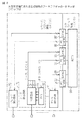
図8は本発明が適用される受信回路のアーキテクチャの一例を示すブロック図であり、並列レシーバのアーキテクチャを示すものである。図8において、参照符号10はデータ検出回路(データ検出ユニット)、11は判定回路(検出回路)、12は位相インターポレータ(P/I)、20,20’はシンクロナイザ(SYNC)、30,30’は位相インターポレータカウンタ(PI CNTR)、70はクロック検出回路(クロック検出ユニット)、そして、90は基本制御回路(Basic Control Unit:BCTL部)を示している。
【0033】
受信回路は、第1のクロック(レシーバクロック:CLK1)により駆動されるクロック検出回路70および複数のデータ検出回路10を有するレシーバクロック領域RCDと、BCTL部90を有するコアクロック領域CCD(内部回路5)とを備える。
各データ検出回路10およびクロック検出回路70は、4−way動作を行うようになっており、それぞれ判定回路11(例えば、図7のデータ検出回路1に対応)および位相インターポレータ12(例えば、図7の位相インターポレータ4に対応)を備えている。各位相インターポレータ12には、位相インターポレータカウンタ(PIカウンタ)30,30’の出力が供給され、また、各判定回路11の出力はシンクロナイザ20,20’に供給され、コアロジック(内部回路)に送られる。なお、位相インターポレータ12のコード(位相制御コード)は、コアロジック中のBCTL部90で生成される。
【0034】
図9は図8の受信回路におけるBCTL部90の一例を示すブロック図である。
BCTL部90は、コアロジック領域CCDに設けられ、各シンクロナイザ20,20’および各PIカウンタ30,30’を制御する。すなわち、図9に示されるように、BCTL部90は、第1のフィルタ91、第2のフィルタ92、第3のフィルタ部93、遅延コード発生回路94、加算器95、セレクタ96、レイテンシーカウンタ(LTC CNTR)97,および、制御信号発生部98を備え、各シンクロナイザ20,20’で用いるリードポインタを制御するポインタ制御信号PS、遅延コードDC、各PIカウンタ30,30’に与える制御コード(b0、b1、b2)、および、位相オフセットキャンセル信号POCを生成する。
【0035】
レイテンシーカウンタ97は、出力する信号の符号が逆である点を除くと、PIカウンタ30に類似した構成とされ、位相コードを校正した後、レイテンシーカウンタ97のカウント値からデータの遅延量が分かるようになっている。なお、位相コードの校正によるレイテンシーカウンタ97のリセット動作は、制御信号発生部98からの位相オフセットキャンセル信号POCにより行われる。なお、制御信号発生部98は、位相オフセットキャンセル信号POCだけでなく、受信回路に必要とされる様々な制御信号を発生している。
【0036】
位相オフセットキャンセル信号POCは、図17を参照して後述するように、セレクタ302を制御して、カウンタ301に対する位相コードの校正処理を行うようになっている。また、後述するように(或いは、図7に示されるように)、ポインタ制御信号PSは、シンクロナイザ20,20’(2)が適切なデータパスを選択、すなわち、偶数番目の信号が送出されるEVENパスと奇数番目の信号が送出されるODDパスかを選択するために使用される。
【0037】
図8および図9に示されるように、ディジタルフィルタ(第1のフィルタ91および第2のフィルタ92)は、シンクロナイザ20’を介して供給されるクロック検出回路70からの出力により内部クロックの入カクロックに対する遅れ/進みを判定して処理し、PIカウンタ30’を介してクロック検出回路70の位相インターポレ一夕(12)にフィードバックする。ここで、PIカウンタ30’には第1のフィルタ91の出力が供給され、また、各PIカウンタ30には第2のフィルタ92の出力と第3のフィルタ部93の各出力とが加算器95で加算されたものが供給される。そして、各PIカウンタ30を介して各データ検出回路10の位相インターポレ一夕12にもフィードバック(アップまたはダウン)値が送られる。
【0038】
ここで、シンクロナイザ20,20’は、遅延コードDCにより制御されるが、この遅延コードDCは遅延量をディジタル値で表したものである。また、第3のフィルタ部93は、クロック検出回路70とデータ検出回路10の間のスキュー調整を行うロジック回路を備え、このスキュー調整ロジック回路により各レシーバ(クロック検出回路70およびデータ検出回路10)の位相誤差が最小となるように制御する。
【0039】
図10は図8の受信回路におけるレシーバの判定回路11の一例を示すブロック図である。図10において、参照符号111はイコライザ、112o,113oおよび112e,113eは奇数パス用および偶数パス用データ判定ユニット(D型フリップフロップ:D−FF)、114oおよび114eは奇数パス用および偶数パス用バッファ、そして、115は制御信号発生部を示している。
【0040】
判定回路11は後段のシンクロナイザにデータを渡す役割を果たすが、入力信号はイコライザ(EQRZ)111を介して奇数パス用データ判定ユニット112o,113oおよび偶数パス用データ判定ユニット112e,113eに供給される。ここで、奇数パス用データ判定ユニット112o,113oおよび偶数パス用データ判定ユニット112e,113eは、四相クロック信号(位相が90度異なる2組の相補信号)A,B,AX,BXが供給された制御信号発生部115の出力により交互に駆動されるようになっている。また、各イコライザ(4つのイコライザ)には、それぞれ位相が90度異なる四相クロック信号A,B,AX,BXにより、順次駆動されるようになっている。そして、奇数パス用データ判定ユニット112o,113oおよび偶数パス用データ判定ユニット112e,113eの出力は、それぞれバッファ114oおよび114eを介してデータD0(D0〜D3)として出力される。
【0041】
ここで、四相クロック信号A,B,AX,BXは、位相インターポレータ12の出力として判定回路11に入力され、また、データD0〜D3およびデータクロック信号DCLKは、シンクロナイザ(シンクロナイザの後半部分)20へ出力される。
図11は図8の受信回路におけるシンクロナイザ20の一例を示すブロック図である。図11において、参照符号201はシンクロナイズユニット、202はレジスタ(D−FF)、203は位相比較器(位相検出器)、そして、204はフィルタ(ディジタルフィルタ)を示している。
【0042】
図11に示されるように、シンクロナイザ(シンクロナイザの後半部分)20は、判定回路11からのデータ信号D0〜D3およびデータクロック信号DCLKを受け取ると共に、基本制御回路(BCTL部)90からの遅延コードDCおよびポインタ信号PS、並びに、コアクロック(第2のクロック信号CLK2)を受け取る。
【0043】
各シンクロナイズユニット201は、複数のレジスタ(D−FF)211〜216およびセレクタ217〜219を備えて構成され、セレクタ219で選択されたシンクロナイズユニット201の出力信号がコアクロックCLK2で制御されるレジスタ202を介して出力されることにより、コアクロックCLK2に同期したデータ信号D0’〜D3’が得られる。
【0044】
ここで、セレクタ219は、基本制御回路90からのポインタ信号PSにより制御され、奇数または偶数の信号パス(奇数パス用または偶数パス用バッファ114o,114eの出力)が選択されて出力される。また、セレクタ217および218は遅延コードDCにより制御され、遅延量に応じたレジスタの段数が選択されるようになっている。
【0045】
位相比較器203(例えば、図7における位相比較器61に対応)は、データクロック信号DCLKとコアクロックCLK2の位相を比較し、その出力をフィルタ204(例えば、図4におけるフィルタ63に対応)を介してPIカウンタ30へ供給する。これにより、コアクロック(CLK2)とデータクロック信号DCLKの位相が合い、その結果として、これと特定の位相関係(D−FFのclock-to-Qの時間に相当)にある位相インターポレ一夕のクロック(DCLK)の位相が合う位相コード値が決定(校正)されることになる。
【0046】
図12は図11のシンクロナイザにおける位相比較器(位相検出回路)203およびフィルタ204の一例を示すブロック図であり、図13は図12の位相検出回路におけるコード発生回路の動作を説明するための図である。
図12に示されるように、位相比較器(位相検出器)203は出力レジスタと同様のレジスタ(D−FF)として構成され、また、フィルタ204は、アップダウンカウンタ(例えば、4ビットのアップダウンカウンタ)241、フィルタ部242およびコード発生器243を備えて構成される。そして、データクロック信号DCLKとコアクロックCLK2の位相差に応じてアップダウンカウンタ241を制御し、フィルタ242の出力U,Dに応じて図13に示すような真理値表のコードb2,b0を出力する。
【0047】
図14は図11のシンクロナイザの動作を説明するためのタイミング図であり、偶数の信号パスの動作を説明するものである。なお、奇数の信号パスも同様である。図14において、参照符号PPは、入力された4ビットの最初のクロック『0』からこの4ビットデータを並列に出力するまでのレイテンシーが零(3UI+td:ここで、tdはレジスタの遅延)のタイミングを示し、また、Tminは読み出し最小時間(3UI+td+(0〜6UI):ここで、0〜6UIは読み出しマージン)を示す。
【0048】
図9を参照して説明したように、位相コードを校正した後のデータの遅延は、基本制御回路(BCTL部)90におけるレイテンシーカウンタ97の値により分かる。このレイテンシーカウンタ97の値を使用して遅延コードDCおよびポインタ信号PSを発生する。
図14ではレイテンシーコードの上位4ビットが示されており、遅延コードDCによって、セレクタ(図11における偶数の信号パスのセレクタ)218が制御される。すなわち、上位4ビットのレイテンシーコードが『0000』,『0001』,『0010』のとき、図11のセレクタ218は信号パスR00(レジスタを通らないパス)を選択し、また、レイテンシーコードが『0011』,『0100』のとき、セレクタ218は信号パスR01(レジスタ214だけを通るパス)を選択し、さらに、レイテンシーコードが『0101』,『0110』のとき、セレクタ218は信号パスR10(レジスタ214および215を通るパス)を選択し、そして、レイテンシーコードが『0111』,『1000』,『1001』のとき、セレクタ218は信号パスR11(全てのレジスタ214〜216を通るパス)を選択する。
【0049】
ここで、ポインタ信号PSは、基本的には『0101』とトグルを続けるが、シンクロナイザ20の遅延が限界値を超えて大きく(或いは、小さく)なると、基本制御回路90によりトグルしないように制御し(例えば、『0101011010…』(『…11…』))、それと同時に、例えば、レイテンシーコードを4UI(単位間隔:Unit Interval)だけシフトする。なお、このレイテンシーコードのシフト処理が行われるときのデータは使用せずに廃棄することになるが、これは、例えば、入力信号(受信回路に伝えられるデータ信号)の所定ビット毎にそのための補償用データを挿入しておく。この補償用データは、例えば、最初の符号が特殊符号(Null Symbol)で4ビットのデータとして構成される。
【0050】
なお、位相コードの校正は、例えば、電源の投入時等において、4ビット周期のトレーニングパターンの入力信号『1000100010001…』を与えて行うようになっている。そして、シンクロナイザ20で使用する遅延コードは、図14に示されるようなレイテンシーコードに基づいて発生される。
図15は図8の受信回路における先読み特殊符号発生ユニットの一例を示すブロック図である。
【0051】
図15に示されるように、先読み特殊符号発生ユニット220は、図11に示すようなシンクロナイズユニット201と類似の構成とされ、複数のレジスタ(D−FF)221〜224、セレクタ225〜227、および、出力レジスタ(D−FF)228を備えて構成される。すなわち、例えば、受信回路に対してシリアルに送られてくる4ビットデータの最初の1ビット(レジスタ112o,112e)の出力信号だけ、バッファ144o,144eを介して先読み特殊符号発生ユニット220に供給され、これにより、パラレルに出力されるデータD0〜D3よりも早いタイミング(3UI程度早いタイミング)で、特殊符号(4ビットの補償用データの最初の1ビット)nを検出することができるようになっている。
【0052】
図16は図15のシンクロナイザの動作を説明するためのタイミング図である。
図14と図16との比較から明らかなように、図15に示すシンクロナイザにおける先読み特殊符号発生ユニット220は、図11と類似した動作を行って遅延コードがレイテンシーコードに基づいて発生される。なお、上述した特殊符号(Null Symbol)を他のデータよりも先に確認することによって、補償用データによる処理を行うようになっている。
【0053】
図17は図8の受信回路における位相インターポレータ12とシンクロナイザ20との間のインターフェース回路(PI制御回路)30の一例を示すブロック図である。
図17に示されるように、インターフェース回路30は、カウンタ301およびセレクタ302を備え、シンクロナイザ20の出力(フィルタ204からの出力コード)b2,b1(=0),b0と基本制御回路90からのコードb2’,b1’,b0’とを位相オフセットキャンセル信号POCによりセレクタ302で選択して、カウンタ301に供給する。そして、カウンタ301によりカウントされた位相コード(グレーコード:Gray Code)は、位相インターポレータ12に供給される。
【0054】
ここで、位相オフセットキャンセル信号POCが『1』のとき、セレクタ302はシンクロナイザ20からのコードを選択することになり、ローカルな帰還ループが形成されて位相コードの校正が行われる。また、位相オフセットキャンセル信号POCが『0』のときには、基本制御回路90からの出力コードが選択されてそれがカウンタ301に供給される。
【0055】
図18は図8の受信回路における位相インターポレータ12の一例を示すブロック図である。
図18に示されるように、位相インターポレータ12は、コード変換部121、D/Aコンバータ122、位相インターポレータコア123、および、分周器124を備えている。
【0056】
コード変換部121は、カウンタ301(インターフェース回路30)からの位相コード(グレーコード)をサモメタコード(Thermometer Code)に変換してD/Aコンバータ122に供給し、このD/Aコンバータ122は、供給されたサモメタコードをアナログ信号に変換して位相インターポレータコア123に供給する。
【0057】
位相インターポレータコア123は、ミキサおよび比較器を備え、例えば、PLL回路からの四相クロック信号(例えば、800MHz)に対してD/Aコンバータ122の出力で重み付けを行って任意の位相を有する二相クロック信号(例えば、800MHz)を分周器124に出力する。分周器124は、入力された二相クロック信号を分周してそれぞれ位相が90度異なる四相クロック信号(位相が90度異なる2組の相補信号)A,B,AX,BX(例えば、400MHz)を発生し、この四相クロック信号が判定回路11に供給されることになる。
【0058】
(付記1) 基準クロック信号を受け取り、ディジタルコードで出力位相を制御して第1のクロック信号を発生するクロック信号発生手段と、
該第1のクロック信号で動作する回路群と第2のクロック信号で動作する内部回路との間で信号の受け渡しを行うシンクロナイズ手段と、
前記第1のクロック信号と前記第2のクロック信号の位相が特定の関係にあるときの位相コードを認識する位相コード認識手段と、
該認識された位相コードの値と前記第1および第2のクロック信号の位相差との関係を校正する校正手段とを備え、該校正手段により校正された位相コード情報を使って前記シンクロナイズ手段を制御することを特徴とするタイミング信号発生システム。
【0059】
(付記2) 付記1に記載のタイミング信号発生システムにおいて、前記第2のクロック信号の周期と前記基準クロック信号の周期とは整数倍の関係にあることを特徴とするタイミング発生回路。
(付記3) 付記1に記載のタイミング信号発生システムにおいて、前記クロック信号発生手段は、位相インターポレータであることを特徴とするタイミング発生回路。
【0060】
(付記4) 付記1に記載のタイミング信号発生システムにおいて、前記校正手段による位相コード値と第1および第2のクロック信号の位相差との校正を、該タイミング信号発生システムを設けた装置の電源投入時に実行することを特徴とするタイミング発生回路。
(付記5) 付記1に記載のタイミング信号発生システムにおいて、前記シンクロナイズ手段は、
前記第1のクロック信号で駆動される第1のD型フリップフロップと、
該第1のD型フリップフロップから出力される繰り返し信号を前記第2のクロック信号で駆動されてラッチする第2のD型フリップフロップとを備えることを特徴とするタイミング信号発生システム。
【0061】
(付記6) 付記1に記載のタイミング信号発生システムにおいて、前記シンクロナイズ手段は、
前記第1のクロック信号で駆動されるセレクタと、
該セレクタから出力される繰り返し信号を前記第2のクロック信号で駆動されてラッチするD型フリップフロップとを備えることを特徴とするタイミング信号発生システム。
【0062】
(付記7) 付記1に記載のタイミング信号発生システムにおいて、さらに、
前記第1のクロック信号と前記第2のクロック信号の位相比較を行う位相比較器と、
該位相比較器の出力を処理して前記位相コードに帰還をかける帰還ループを備え、該帰還ループを動作させて前記第1および第2のクロック信号の位相差を所定の値にするときの位相コードを認識することを特徴とするタイミング信号発生システム。
【0063】
(付記8) 付記7に記載のタイミング信号発生システムにおいて、前記位相比較器は、
前記第1のクロック信号で駆動される第1のD型フリップフロップと、
該第1のD型フリップフロップから出力される繰り返し信号を前記第2のクロック信号で駆動されてラッチする第2のD型フリップフロップとを備えることを特徴とするタイミング信号発生システム。
【0064】
(付記9) 付記7に記載のタイミング信号発生システムにおいて、前記位相比較器は、
前記第1のクロック信号で駆動されるセレクタと、
該セレクタから出力される繰り返し信号を前記第2のクロック信号で駆動されてラッチするD型フリップフロップとを備えることを特徴とするタイミング信号発生システム。
【0065】
(付記10) 付記1に記載のタイミング信号発生システムにおいて、前記校正手段は、前記第1および第2のクロック信号の位相差が所定の値になったタイミングで零にリセットされ、その後は前記位相コードと同様に変化するカウンタを備えることを特徴とするタイミング信号発生システム。
(付記11) 付記1に記載のタイミング信号発生システムにおいて、前記校正手段は、前記第1および第2のクロック信号の位相差が所定の値になったときの位相コードの値をオフセット値として記憶する記憶手段を備えることを特徴とするタイミング信号発生システム。
【0066】
(付記12) 付記10または11のいずれか1項に記載のタイミング信号発生システムにおいて、前記シンクロナイズ手段をFIFOと等価な回路で構成し、該FIFOの書き込みポインタの値および前記位相コードの値を用いて当該FIFOの読み出しポインタの値を決定することを特徴とするタイミング信号発生システム。
【0067】
(付記13) 入力信号からクロック信号を再生し、該再生されたクロック信号を用いて該入力信号のデータを読み出す受信回路であって、
基準クロック信号を受け取り、ディジタルコードで出力位相を制御して第1のクロック信号を発生するクロック信号発生手段と、
該第1のクロック信号で動作する回路群と第2のクロック信号で動作する内部回路との間で信号の受け渡しを行うシンクロナイズ手段と、
前記第1のクロック信号と前記第2のクロック信号の位相が特定の関係にあるときの位相コードを認識する位相コード認識手段と、
該認識された位相コードの値と前記第1および第2のクロック信号の位相差との関係を校正する校正手段とを備え、該校正手段により校正された位相コード情報を使って前記シンクロナイズ手段を制御することを特徴とする受信回路。
【0068】
(付記14) 付記13に記載の受信回路において、
前記第1のクロック信号で動作する回路群は、前記入力信号からデータを検出するためのデータ検出回路、および、該入力信号からクロックを再生するためのクロック検出回路を備え、
前記第2のクロック信号で動作する内部回路は、前記クロック信号発生手段を制御する基本制御回路を備えることを特徴とする受信回路。
【0069】
(付記15) 付記14に記載の受信回路において、
前記データ検出回路は、第1のクロック信号群により駆動される複数のデータ検出ユニットを備え、
前記クロック検出回路は、前記第1のクロック信号群と所定の位相差だけ異なる第2のクロック信号群により駆動される複数のクロック検出ユニットを備えることを特徴とする受信回路。
【0070】
(付記16) 付記14に記載の受信回路において、前記データ検出回路および前記クロック検出回路は偶数の信号パスおよび奇数の信号パスを有し、ポイント制御信号に応じて該偶数または奇数のいずれかの信号パスを選択するようになっていることを特徴とする受信回路。
(付記17) 付記13に記載の受信回路において、前記第2のクロック信号の周期と前記基準クロック信号の周期とは整数倍の関係にあることを特徴とする受信回路。
【0071】
(付記18) 付記13に記載の受信回路において、前記クロック信号発生手段は、位相インターポレータであることを特徴とする受信回路。
(付記19) 付記13に記載の受信回路において、前記校正手段による位相コード値と第1および第2のクロック信号の位相差との校正を、該受信回路を設けた装置の電源投入時に実行することを特徴とする受信回路。
【0072】
(付記20) 付記13に記載の受信回路において、前記シンクロナイズ手段は、
前記第1のクロック信号で駆動される第1のD型フリップフロップと、
該第1のD型フリップフロップから出力される繰り返し信号を前記第2のクロック信号で駆動されてラッチする第2のD型フリップフロップとを備えることを特徴とする受信回路。
【0073】
(付記21) 付記13に記載の受信回路において、前記シンクロナイズ手段は、
前記第1のクロック信号で駆動されるセレクタと、
該セレクタから出力される繰り返し信号を前記第2のクロック信号で駆動されてラッチするD型フリップフロップとを備えることを特徴とする受信回路。
【0074】
(付記22) 付記13に記載の受信回路において、さらに、
前記第1のクロック信号と前記第2のクロック信号の位相比較を行う位相比較器と、
該位相比較器の出力を処理して前記位相コードに帰還をかける帰還ループを備え、該帰還ループを動作させて前記第1および第2のクロック信号の位相差を所定の値にするときの位相コードを認識することを特徴とする受信回路。
【0075】
(付記23) 付記22に記載の受信回路において、前記位相比較器は、
前記第1のクロック信号で駆動される第1のD型フリップフロップと、
該第1のD型フリップフロップから出力される繰り返し信号を前記第2のクロック信号で駆動されてラッチする第2のD型フリップフロップとを備えることを特徴とする受信回路。
【0076】
(付記24) 付記22に記載の受信回路において、前記位相比較器は、
前記第1のクロック信号で駆動されるセレクタと、
該セレクタから出力される繰り返し信号を前記第2のクロック信号で駆動されてラッチするD型フリップフロップとを備えることを特徴とする受信回路。
(付記25) 付記13に記載の受信回路において、前記校正手段は、前記第1および第2のクロック信号の位相差が所定の値になったタイミングで零にリセットされ、その後は前記位相コードと同様に変化するカウンタを備えることを特徴とする受信回路。
【0077】
(付記26) 付記13に記載の受信回路において、前記校正手段は、前記第1および第2のクロック信号の位相差が所定の値になったときの位相コードの値をオフセット値として記憶する記憶手段を備えることを特徴とする受信回路。
(付記27) 付記25または26のいずれか1項に記載の受信回路において、前記シンクロナイズ手段をFIFOと等価な回路で構成し、該FIFOの書き込みポインタの値および前記位相コードの値を用いて当該FIFOの読み出しポインタの値を決定することを特徴とする受信回路。
【0078】
【発明の効果】
以上、詳述したように、本発明によれば、高速信号の受信に使うクロック信号と内部回路の駆動クロック信号との位相関係を、位相検出回路を常時動作させることなく全ての位相範囲に渡って正確に知ることができるため、低レイテンシーでしかもメタステーブル状態の可能性のないシンクロナイザを実現することができる。従って、シンクロナイザを有するタイミング信号発生システム(受信回路)を、より少ない回路量で構成すると共に、短い処理時間で動作させることができる。
【図面の簡単な説明】
【図1】従来のタイミング信号発生システム(受信回路)の一例を示すブロック図である。
【図2】本発明に係るタイミング信号発生システム(受信回路)の原理構成を示すブロック図である。
【図3】本発明のタイミング信号発生システムの第1実施例を示すブロック図である。
【図4】本発明のタイミング信号発生システムの第2実施例を示すブロック図である。
【図5】本発明のタイミング信号発生システムの第3実施例を示すブロック図である。
【図6】本発明のタイミング信号発生システムの第4実施例を示すブロック図である。
【図7】本発明のタイミング信号発生システムの第5実施例を示すブロック図である。
【図8】本発明が適用される受信回路のアーキテクチャの一例を示すブロック図である。
【図9】図8の受信回路におけるBCTL部の一例を示すブロック図である。
【図10】図8の受信回路におけるレシーバの判定回路の一例を示すブロック図である。
【図11】図8の受信回路におけるシンクロナイザの一例を示すブロック図である。
【図12】図11のシンクロナイザにおける位相比較器およびフィルタの一例を示すブロック図である。
【図13】図12の位相検出回路におけるコード発生回路の動作を説明するための図である。
【図14】図11のシンクロナイザの動作を説明するためのタイミング図である。
【図15】図8の受信回路における先読み特殊符号発生ユニットの一例を示すブロック図である。
【図16】図15のシンクロナイザの動作を説明するためのタイミング図である。
【図17】図8の受信回路における位相インターポレータとシンクロナイザとの間のインターフェース回路の一例を示すブロック図である。
【図18】図8の受信回路における位相インターポレータの一例を示すブロック図である。
【符号の説明】
1,10…データ検出回路(データ検出回路ユニット)
2,20,20’…シンクロナイザ
3…制御回路
4…ディレイエレメント(位相インターポレータ)
5…内部回路
6…PLL回路
7,70…クロック検出回路(クロック検出回路ユニット)
8…位相比較器(位相検出器)
9…フィルタ(ディジタルフィルタ)
11…判定回路(検出回路)
12…位相インターポレータ
30,30’…位相インターポレータカウンタ(PIカウンタ)
31…コード認識回路
32…アップダウンカウンタ
33…レジスタ
60…ディジタルループフィルタ
61…位相比較器
62…分周器
63…フィルタ(アップダウンカウンタ)
64…セレクタ
90…基本制御回路(BCTL部)
91…第1のフィルタ
92…第2のフィルタ
93…第3のフィルタ部(スキュー調整ロジック回路)
94…遅延コード発生回路
95…加算器
96…セレクタ
97…レイテンシーカウンタ
98…制御信号発生部
201…シンクロナイズユニット
202…レジスタ(D−FF)
203…位相比較器(位相検出器)
204…フィルタ(ディジタルフィルタ)
220…先読み特殊符号発生ユニット[0001]
BACKGROUND OF THE INVENTION
The present invention relates to a signal transmission technique for performing high-speed signal transmission between a plurality of LSI chips or between a plurality of elements and circuit blocks in one chip, or between a plurality of boards or a plurality of enclosures. In particular, the present invention relates to a timing signal generation system and a receiving circuit for performing high-speed signal transmission.
[0002]
In recent years, the performance of components constituting computers and other information processing devices has greatly improved. For example, the performance of semiconductor storage devices such as SRAM (Static Random Access Memory) and DRAM (Dynamic Random Access Memory) and processors has been improved. There is something that is amazing. As the performance of the semiconductor memory device, processor, etc. is improved, the performance of the system cannot be improved unless the signal transmission speed between components or elements is improved. Specifically, for example, a signal transmission speed between a main storage device such as a DRAM and a processor (between LSIs) is becoming an obstacle to improving the performance of the entire computer. Furthermore, not only signal transmission between the chassis and the board (printed wiring board) such as between the server and the main storage device or the server via the network, but also high integration and enlargement of the semiconductor chip and low power supply voltage. Due to (lowering of signal amplitude level) and the like, it is necessary to improve the signal transmission speed in signal transmission between chips and signal transmission between elements and circuit blocks in the chip. In order to realize such high-speed signal transmission, a timing signal generation system (reception circuit) having a synchronizer is required. However, it is desired to provide a timing signal generation system with a smaller circuit amount and a short processing time. ing.
[0003]
[Prior art]
In recent years, it is necessary to increase the signal transmission speed per pin in order to cope with an increase in the amount of data transmission between LSIs and boards or between enclosures. This is also to avoid an increase in the cost of the package and the like due to an increase in the number of pins. As a result, recently, the signal transmission speed between LSIs exceeds 1 Gbps, and in the future (about 3 to 8 years ahead), it is expected to become extremely high values (high-speed signal transmission) such as 4 Gbps or 10 Gbps. Yes.
[0004]
At such a high signal frequency, the delay of the buffer and wiring for transmitting data and clock signals is a non-negligible ratio to the clock signal period (in some cases, it can be many times the clock signal period). Occupy. Here, the phase of the transmitted clock signal can be considered to be completely independent of the phase of the clock signal used for the operation of the internal circuit of the chip. Therefore, in order to transfer the signal from the clock signal region used for receiving the high-speed signal to the clock signal region used in the internal circuit, a synchronizer that performs so-called clock signal transfer is required.
[0005]
FIG. 1 is a block diagram showing an example of a conventional timing signal generation system (reception circuit). In FIG. 1,
As shown in FIG. 1, an input signal (for example, a high-speed signal supplied via a transmission path) is supplied to the
[0006]
The
[0007]
[Problems to be solved by the invention]
As described above, the
[0008]
At this time, if the timing of writing and reading is not properly selected, for example, if the phases of the external clock signal CLK1 and the internal clock signal CLK2 match, data cannot be read correctly, or the output of the D-FF is “ There arises a problem that reading is performed in an intermediate state between “0” and “1” (meta-stable state).
[0009]
In order to avoid such a problem, it is necessary to always monitor the phase difference between the external clock signal CLK1 and the internal clock signal CLK2. However, the circuit (phase comparator 104) that detects the phase difference between the two clock signals itself is required. It is necessary to have sufficient delay to avoid metastable state. As a result, the conventional timing signal generation system provided with a synchronizer for changing clock signals has problems to be solved such as an increase in circuit amount and an increase in processing time.
[0010]
The present invention has been made in view of the above-described problems of the conventional timing signal generation system (reception circuit) and provides a timing signal generation system with a smaller circuit amount and a shorter processing time.
[0011]
[Means for Solving the Problems]
Main departure Enlightenment According to the embodiment, it comprises a clock signal generation means, a synchronization means, a phase code recognition means, and a calibration means. Receiving circuit that regenerates clock signal from input signal and reads data of the input signal using the regenerated clock signal Is provided.
The clock signal generating means receives the reference clock signal and controls the output phase with a digital code to generate a first clock signal. The synchronizing means includes a circuit group operating with the first clock signal and a second clock signal. Signals are exchanged with an internal circuit that operates with a clock signal. The phase code recognizing means has a phase relationship between the phase of the first clock signal and the second clock signal in a specific relationship. Generated from a signal processed by a group of circuits operating with a first clock signal The phase code is recognized (measured), and the calibration unit calibrates the relationship between the recognized phase code value and the phase difference between the first and second clock signals.
[0013]
Of the present invention Implementation In the form, the phase code information calibrated by the calibration means is used. So as to convert a signal synchronized with the first clock signal into a signal synchronized with the second clock signal, The synchronization means is controlled.
FIG. 2 is a block diagram showing the principle configuration of the timing signal generation system (reception circuit) according to the present invention. In FIG. 2,
[0014]
As shown in FIG. 2, the timing signal generation system (reception circuit) according to the present invention uses a
[0015]
The
However, since the phase relationship between the value of the phase code PC and the clock signal (internal circuit driving clock signal) CLK2 driving the
[0016]
Therefore, in the present invention, means (calibration means) for calibrating the relationship between the value of the phase code PC and the internal circuit driving clock signal CLK2 is provided. This is because the phase relationship between the output clock signal of the phase interpolator 4 (the clock signal supplied to the data detection circuit 1) and the internal circuit driving clock signal CLK2 is a specific relationship (for example, the rising edges match). This corresponds to recording the value of the phase code PC in a state in (). Once the relationship between the phase code value and the phase difference is clarified, the write timing (first clock signal CLK1) and read timing (second clock signal CLK2) in the
[0017]
This calibration operation is performed temporarily by a phase comparison loop including a phase interpolator and a calibration phase comparator (a circuit that compares the phase of the output clock signal of the phase interpolator and the phase of the clock signal for driving the internal circuit). This is also possible by observing the phase code in a state of being configured and locked in phase.
As described above, according to the timing signal generation system (reception circuit) of the present invention, the read timing of the synchronizer can be controlled by directly using the phase code obtained from the high-speed signal receiver, and the circuit always performs the phase comparison. Compared with the control, the delay time can be reduced and control can be performed. In the present invention, once the calibration operation is performed, it is not necessary to operate the phase comparator thereafter, and the problem of metastable due to the phase comparison does not occur. Further, observing the phase code of the phase interpolator can know the phase with higher resolution than the phase comparator, and a low latency synchronizer can be configured.
[0018]
DETAILED DESCRIPTION OF THE INVENTION
Embodiments of a timing signal generating system (receiving circuit) according to the present invention will be described in detail below with reference to the accompanying drawings.
FIG. 3 is a block diagram showing a first embodiment of the timing signal generating system of the present invention. In FIG. 3,
[0019]
As shown in FIG. 3, in the timing signal generation system of the first embodiment, the input signal is a 2.5 Gbps high-speed signal, and each of the high-speed input signals is, for example, a 625 MHz four-phase clock signal. The data is supplied to the
[0020]
Each of the 625 MHz four-phase clock signals supplied to the
[0021]
The
Here, the data output from the
[0022]
In the timing signal generation system of the first embodiment, the output of the
[0023]
Thereafter, the up / down
[0024]
The timing signal generation system of the first embodiment uses the value of the up / down counter 32 described above to control the read address of the RAM used for the
FIG. 4 is a block diagram showing a second embodiment of the timing signal generating system of the present invention. In FIG. 4,
[0025]
As shown in FIG. 4, the timing signal generation system of the second embodiment is a temporary phase-locked loop in which the phase difference between the two clock signals CLK1 and CLK2 is made zero at power-on (startup). Form. That is, at the time of power-on, the
[0026]
Next, when the power-on time ends, the
As described above, in the timing signal generation system of the second embodiment, the phase code (PC0) having a phase difference of zero is automatically found by the feedback loop, and calibration can be performed with a minimum number of additional circuits.
FIG. 5 is a block diagram showing a third embodiment of the timing signal generating system of the present invention. In FIG. 5,
[0027]
As apparent from the comparison between FIG. 2 and FIG. 5, the timing signal generating system of the third embodiment is provided with a
That is, in the timing signal generating system of the third embodiment, the phase of the two clock signals CLK1 and CLK2 is aligned by the
[0028]
FIG. 6 is a block diagram showing a fourth embodiment of the timing signal generating system of the present invention.
As shown in FIG. 6, the timing signal generation system of the fourth embodiment is configured such that the
[0029]
That is, in the timing signal generation system of the fourth embodiment, the
[0030]
FIG. 7 is a block diagram showing a fifth embodiment of the timing signal generating system of the present invention.
As is apparent from the comparison between FIG. 6 and FIG. 7, the timing signal generation system of the fifth embodiment has a first clock signal (data detection circuit) for the
[0031]
That is, in the timing signal generation system of the fifth embodiment, the
[0032]
In the fifth embodiment, the delay (clock-to-Q delay) of the detection (determination) circuit used in the
FIG. 8 is a block diagram showing an example of the architecture of a receiving circuit to which the present invention is applied, and shows the architecture of a parallel receiver. In FIG. 8,
[0033]
The receiving circuit includes a receiver clock region RCD having a
Each
[0034]
FIG. 9 is a block diagram showing an example of the
The
[0035]
The
[0036]
As will be described later with reference to FIG. 17, the phase offset cancel signal POC controls the
[0037]
As shown in FIGS. 8 and 9, the digital filter (the
[0038]
Here, the
[0039]
FIG. 10 is a block diagram showing an example of the
[0040]
The
[0041]
Here, the four-phase clock signals A, B, AX, and BX are input to the
FIG. 11 is a block diagram showing an example of the
[0042]
As shown in FIG. 11, the synchronizer (second half part of the synchronizer) 20 receives the data signals D0 to D3 and the data clock signal DCLK from the
[0043]
Each
[0044]
Here, the
[0045]
The phase comparator 203 (for example, corresponding to the
[0046]
12 is a block diagram showing an example of the phase comparator (phase detection circuit) 203 and the
As shown in FIG. 12, the phase comparator (phase detector) 203 is configured as a register (D-FF) similar to the output register, and the
[0047]
FIG. 14 is a timing chart for explaining the operation of the synchronizer of FIG. 11, and is for explaining the operation of even-numbered signal paths. The same applies to odd signal paths. In FIG. 14, reference symbol PP indicates a timing at which the latency from the input 4-bit first clock “0” to the output of the 4-bit data in parallel is zero (3UI + td, where td is a delay of the register). Tmin represents a minimum read time (3 UI + td + (0-6 UI): where 0-6 UI is a read margin).
[0048]
As described with reference to FIG. 9, the delay of the data after the phase code is calibrated is known from the value of the
FIG. 14 shows the upper 4 bits of the latency code, and the selector (the selector of the even signal path in FIG. 11) 218 is controlled by the delay code DC. That is, when the latency code of the upper 4 bits is “0000”, “0001”, “0010”, the
[0049]
Here, the pointer signal PS continues to toggle “0101” basically, but when the delay of the
[0050]
The phase code is calibrated by giving a 4-bit cycle training pattern input signal “1000100010001...” When the power is turned on, for example. The delay code used in the
FIG. 15 is a block diagram showing an example of a prefetch special code generation unit in the receiving circuit of FIG.
[0051]
As shown in FIG. 15, the prefetch special
[0052]
FIG. 16 is a timing chart for explaining the operation of the synchronizer of FIG.
As is clear from the comparison between FIG. 14 and FIG. 16, the look-ahead special
[0053]
FIG. 17 is a block diagram showing an example of an interface circuit (PI control circuit) 30 between the
As shown in FIG. 17, the
[0054]
Here, when the phase offset cancel signal POC is “1”, the
[0055]
FIG. 18 is a block diagram showing an example of the
As illustrated in FIG. 18, the
[0056]
The
[0057]
The
[0058]
(Supplementary note 1) Clock signal generating means for receiving a reference clock signal and controlling the output phase with a digital code to generate a first clock signal;
Synchronization means for passing signals between a circuit group operating with the first clock signal and an internal circuit operating with the second clock signal;
Phase code recognition means for recognizing a phase code when the phases of the first clock signal and the second clock signal are in a specific relationship;
Calibration means for calibrating the relationship between the recognized phase code value and the phase difference between the first and second clock signals, and using the phase code information calibrated by the calibration means, A timing signal generation system characterized by controlling.
[0059]
(Supplementary note 2) The timing signal generation system according to
(Supplementary note 3) The timing signal generation system according to
[0060]
(Supplementary note 4) In the timing signal generating system according to
(Supplementary Note 5) In the timing signal generation system according to
A first D-type flip-flop driven by the first clock signal;
A timing signal generating system comprising: a second D-type flip-flop that is driven by the second clock signal and latches a repetitive signal output from the first D-type flip-flop.
[0061]
(Supplementary Note 6) In the timing signal generation system according to
A selector driven by the first clock signal;
A timing signal generating system comprising: a D-type flip-flop that is driven by the second clock signal and latches a repetitive signal output from the selector.
[0062]
(Appendix 7) In the timing signal generation system according to
A phase comparator for performing phase comparison between the first clock signal and the second clock signal;
A phase at which the output of the phase comparator is processed to feed back the phase code and the phase difference between the first and second clock signals is set to a predetermined value by operating the feedback loop; A timing signal generation system characterized by recognizing a code.
[0063]
(Supplementary note 8) In the timing signal generation system according to
A first D-type flip-flop driven by the first clock signal;
A timing signal generating system comprising: a second D-type flip-flop that is driven by the second clock signal and latches a repetitive signal output from the first D-type flip-flop.
[0064]
(Supplementary note 9) In the timing signal generation system according to
A selector driven by the first clock signal;
A timing signal generating system comprising: a D-type flip-flop that is driven by the second clock signal and latches a repetitive signal output from the selector.
[0065]
(Supplementary note 10) In the timing signal generating system according to
(Supplementary Note 11) In the timing signal generation system according to
[0066]
(Supplementary Note 12) In the timing signal generation system according to any one of
[0067]
(Supplementary note 13) A reception circuit that reproduces a clock signal from an input signal and reads data of the input signal using the regenerated clock signal,
Clock signal generating means for receiving a reference clock signal and controlling the output phase with a digital code to generate a first clock signal;
Synchronization means for passing signals between a circuit group operating with the first clock signal and an internal circuit operating with the second clock signal;
Phase code recognition means for recognizing a phase code when the phases of the first clock signal and the second clock signal are in a specific relationship;
Calibration means for calibrating the relationship between the recognized phase code value and the phase difference between the first and second clock signals, and using the phase code information calibrated by the calibration means, A receiving circuit characterized by controlling.
[0068]
(Supplementary note 14) In the reception circuit according to supplementary note 13,
The circuit group operating with the first clock signal includes a data detection circuit for detecting data from the input signal, and a clock detection circuit for recovering a clock from the input signal,
An internal circuit operating with the second clock signal comprises a basic control circuit for controlling the clock signal generating means.
[0069]
(Supplementary Note 15) In the reception circuit according to Supplementary Note 14,
The data detection circuit includes a plurality of data detection units driven by a first clock signal group,
The clock detection circuit includes a plurality of clock detection units driven by a second clock signal group different from the first clock signal group by a predetermined phase difference.
[0070]
(Supplementary note 16) In the reception circuit according to supplementary note 14, the data detection circuit and the clock detection circuit have an even number of signal paths and an odd number of signal paths, and either the even number or the odd number according to a point control signal. A receiving circuit, wherein a signal path is selected.
(Supplementary note 17) The reception circuit according to supplementary note 13, wherein a period of the second clock signal and a period of the reference clock signal are in an integer multiple relationship.
[0071]
(Supplementary note 18) The reception circuit according to supplementary note 13, wherein the clock signal generating means is a phase interpolator.
(Supplementary note 19) In the reception circuit according to supplementary note 13, the calibration of the phase code value by the calibration means and the phase difference between the first and second clock signals is executed when the device provided with the reception circuit is turned on. A receiving circuit.
[0072]
(Supplementary note 20) In the reception circuit according to supplementary note 13, the synchronization means includes:
A first D-type flip-flop driven by the first clock signal;
A receiving circuit comprising: a second D-type flip-flop that is driven by the second clock signal and latches a repetitive signal output from the first D-type flip-flop.
[0073]
(Supplementary note 21) In the reception circuit according to supplementary note 13, the synchronization means includes:
A selector driven by the first clock signal;
A receiving circuit comprising: a D-type flip-flop that is driven by the second clock signal and latches a repetitive signal output from the selector.
[0074]
(Supplementary note 22) In the reception circuit according to supplementary note 13, further,
A phase comparator for performing phase comparison between the first clock signal and the second clock signal;
A phase at which the output of the phase comparator is processed to feed back the phase code and the phase difference between the first and second clock signals is set to a predetermined value by operating the feedback loop; A receiving circuit characterized by recognizing a code.
[0075]
(Supplementary note 23) In the reception circuit according to supplementary note 22, the phase comparator includes:
A first D-type flip-flop driven by the first clock signal;
A receiving circuit comprising: a second D-type flip-flop that is driven by the second clock signal and latches a repetitive signal output from the first D-type flip-flop.
[0076]
(Supplementary Note 24) In the reception circuit according to Supplementary Note 22, the phase comparator includes:
A selector driven by the first clock signal;
A receiving circuit comprising: a D-type flip-flop that is driven by the second clock signal and latches a repetitive signal output from the selector.
(Supplementary note 25) In the reception circuit according to supplementary note 13, the calibration means is reset to zero when the phase difference between the first and second clock signals reaches a predetermined value, and thereafter the phase code and A receiving circuit comprising a counter that changes in the same manner.
[0077]
(Supplementary note 26) In the reception circuit according to supplementary note 13, the calibration unit stores the value of the phase code when the phase difference between the first and second clock signals becomes a predetermined value as an offset value. A receiving circuit comprising: means.
(Supplementary note 27) In the reception circuit according to any one of supplementary notes 25 or 26, the synchronization means is configured by a circuit equivalent to a FIFO, and the value of the write pointer of the FIFO and the value of the phase code are used to A receiving circuit for determining a read pointer value of a FIFO.
[0078]
【The invention's effect】
As described above in detail, according to the present invention, the phase relationship between the clock signal used for receiving the high-speed signal and the drive clock signal of the internal circuit is extended over the entire phase range without always operating the phase detection circuit. Therefore, it is possible to realize a synchronizer with low latency and no possibility of metastable state. Therefore, the timing signal generation system (reception circuit) having the synchronizer can be configured with a smaller circuit amount and can be operated in a short processing time.
[Brief description of the drawings]
FIG. 1 is a block diagram showing an example of a conventional timing signal generation system (reception circuit).
FIG. 2 is a block diagram showing a principle configuration of a timing signal generation system (reception circuit) according to the present invention.
FIG. 3 is a block diagram showing a first embodiment of a timing signal generating system according to the present invention.
FIG. 4 is a block diagram showing a second embodiment of the timing signal generation system of the present invention.
FIG. 5 is a block diagram showing a third embodiment of the timing signal generating system of the present invention.
FIG. 6 is a block diagram showing a fourth embodiment of the timing signal generating system of the present invention.
FIG. 7 is a block diagram showing a fifth embodiment of the timing signal generating system of the present invention.
FIG. 8 is a block diagram showing an example of an architecture of a receiving circuit to which the present invention is applied.
9 is a block diagram showing an example of a BCTL section in the receiving circuit of FIG.
10 is a block diagram illustrating an example of a receiver determination circuit in the reception circuit of FIG. 8;
11 is a block diagram showing an example of a synchronizer in the receiving circuit of FIG. 8. FIG.
12 is a block diagram illustrating an example of a phase comparator and a filter in the synchronizer of FIG.
13 is a diagram for explaining the operation of the code generation circuit in the phase detection circuit of FIG. 12; FIG.
FIG. 14 is a timing chart for explaining the operation of the synchronizer of FIG. 11;
15 is a block diagram showing an example of a prefetch special code generation unit in the receiving circuit of FIG. 8. FIG.
16 is a timing chart for explaining the operation of the synchronizer of FIG. 15;
17 is a block diagram showing an example of an interface circuit between a phase interpolator and a synchronizer in the receiving circuit of FIG. 8. FIG.
18 is a block diagram illustrating an example of a phase interpolator in the receiving circuit of FIG.
[Explanation of symbols]
1, 10 ... Data detection circuit (data detection circuit unit)
2, 20, 20 '... synchronizer
3 ... Control circuit
4. Delay element (phase interpolator)
5 ... Internal circuit
6 ... PLL circuit
7, 70 ... Clock detection circuit (clock detection circuit unit)
8 ... Phase comparator (phase detector)
9 ... Filter (digital filter)
11: Determination circuit (detection circuit)
12 ... Phase interpolator
30, 30 '... Phase interpolator counter (PI counter)
31. Code recognition circuit
32 ... Up / down counter
33 ... Register
60: Digital loop filter
61 ... Phase comparator
62 ... frequency divider
63 ... Filter (up / down counter)
64 ... selector
90 ... Basic control circuit (BCTL section)
91. First filter
92 ... Second filter
93 ... Third filter section (skew adjustment logic circuit)
94. Delay code generation circuit
95 ... Adder
96 ... selector
97 ... Latency counter
98 ... Control signal generator
201 ... Synchronize unit
202: Register (D-FF)
203 ... Phase comparator (phase detector)
204: Filter (digital filter)
220 ... Prefetch special code generation unit
Claims (9)
基準クロック信号を受け取り、ディジタルコードで出力位相を制御して第1のクロック信号を発生するクロック信号発生手段と、
該第1のクロック信号で動作する回路群と第2のクロック信号で動作する内部回路との間で信号の受け渡しを行うシンクロナイズ手段と、
前記第1のクロック信号と前記第2のクロック信号の位相が特定の関係にあるときの、前記第1のクロック信号で動作する回路群で処理する信号から生成した位相コードを認識する位相コード認識手段と、
該認識された位相コードの値と前記第1および第2のクロック信号の位相差との関係を校正する校正手段とを備え、該校正手段により校正された位相コード情報を使って、前記第1のクロック信号に同期した信号を前記第2のクロック信号に同期した信号に変換するように、前記シンクロナイズ手段を制御することを特徴とする受信回路。A receiving circuit that reproduces a clock signal from an input signal and reads data of the input signal using the reproduced clock signal,
Clock signal generating means for receiving a reference clock signal and controlling the output phase with a digital code to generate a first clock signal;
Synchronization means for passing signals between a circuit group operating with the first clock signal and an internal circuit operating with the second clock signal;
Phase code recognition for recognizing a phase code generated from a signal processed by a circuit group operating on the first clock signal when the phases of the first clock signal and the second clock signal are in a specific relationship Means,
And a calibration means for calibrating the relationship between the phase difference of the recognized values and said first and second clock signals phase code, by using the phase code information calibrated by the calibration unit, said first A receiving circuit which controls the synchronizing means so as to convert a signal synchronized with a clock signal of the second signal into a signal synchronized with the second clock signal .
前記第1のクロック信号で駆動される第1のD型フリップフロップと、
該第1のD型フリップフロップから出力される繰り返し信号を前記第2のクロック信号で駆動されてラッチする第2のD型フリップフロップとを備えることを特徴とする受信回路。The receiving circuit according to claim 1, wherein the synchronizing means includes:
A first D-type flip-flop driven by the first clock signal;
A receiving circuit comprising: a second D-type flip-flop that is driven by the second clock signal and latches a repetitive signal output from the first D-type flip-flop.
前記第1のクロック信号で駆動されるセレクタと、
該セレクタから出力される繰り返し信号を前記第2のクロック信号で駆動されてラッチするD型フリップフロップとを備えることを特徴とする受信回路。The receiving circuit according to claim 1, wherein the synchronizing means includes:
A selector driven by the first clock signal;
A receiving circuit comprising: a D-type flip-flop that is driven by the second clock signal and latches a repetitive signal output from the selector.
前記第1のクロック信号と前記第2のクロック信号の位相比較を行う位相比較器と、
該位相比較器の出力を処理して前記位相コードに帰還をかける帰還ループを備え、該帰還ループを動作させて前記第1および第2のクロック信号の位相差を所定の値にするときの位相コードを認識することを特徴とする受信回路。The receiving circuit according to claim 1, further comprising:
A phase comparator for performing phase comparison between the first clock signal and the second clock signal;
A phase at which the output of the phase comparator is processed to feed back the phase code and the phase difference between the first and second clock signals is set to a predetermined value by operating the feedback loop; A receiving circuit characterized by recognizing a code.
Priority Applications (3)
| Application Number | Priority Date | Filing Date | Title |
|---|---|---|---|
| JP2001189901A JP4672194B2 (en) | 2001-06-22 | 2001-06-22 | Receiver circuit |
| US10/077,875 US7283601B2 (en) | 2001-06-22 | 2002-02-20 | Timing signal generating system and receiving circuit for transmitting signals at high speed with less circuitry |
| EP02251188A EP1271284B1 (en) | 2001-06-22 | 2002-02-21 | Timing signal generating system |
Applications Claiming Priority (1)
| Application Number | Priority Date | Filing Date | Title |
|---|---|---|---|
| JP2001189901A JP4672194B2 (en) | 2001-06-22 | 2001-06-22 | Receiver circuit |
Publications (2)
| Publication Number | Publication Date |
|---|---|
| JP2003008555A JP2003008555A (en) | 2003-01-10 |
| JP4672194B2 true JP4672194B2 (en) | 2011-04-20 |
Family
ID=19028754
Family Applications (1)
| Application Number | Title | Priority Date | Filing Date |
|---|---|---|---|
| JP2001189901A Expired - Fee Related JP4672194B2 (en) | 2001-06-22 | 2001-06-22 | Receiver circuit |
Country Status (3)
| Country | Link |
|---|---|
| US (1) | US7283601B2 (en) |
| EP (1) | EP1271284B1 (en) |
| JP (1) | JP4672194B2 (en) |
Families Citing this family (17)
| Publication number | Priority date | Publication date | Assignee | Title |
|---|---|---|---|---|
| JP3660638B2 (en) * | 2002-03-27 | 2005-06-15 | 株式会社東芝 | Clock extraction circuit |
| DE60219156T2 (en) * | 2002-07-22 | 2007-12-13 | Texas Instruments Inc., Dallas | Method and device for the parallel synchronization of multiple serial data streams |
| US20040088594A1 (en) * | 2002-10-31 | 2004-05-06 | Canagasaby Karthisha S. | Receiver tracking mechanism for an I/O circuit |
| DE60324429D1 (en) * | 2003-09-17 | 2008-12-11 | Verigy Pte Ltd Singapore | Channel with different clock regions |
| JP2006262197A (en) | 2005-03-17 | 2006-09-28 | Fujitsu Ltd | Phase control circuit |
| US7684534B2 (en) * | 2005-07-11 | 2010-03-23 | International Business Machines Corporation | Method and apparatus for handling of clock information in serial link ports |
| US7697647B1 (en) * | 2005-10-03 | 2010-04-13 | Avaya Inc. | Method and system for switching between two (or more) reference signals for clock synchronization |
| JP4749168B2 (en) * | 2006-02-01 | 2011-08-17 | ルネサスエレクトロニクス株式会社 | Clock and data recovery circuit |
| ATE472779T1 (en) * | 2007-12-27 | 2010-07-15 | Em Microelectronic Marin Sa | ELECTRONIC CIRCUIT FOR NOT INITIALIZED ANSWERING MACHINE WHEN THE SUPPLY VOLTAGE IS SWITCHED ON |
| US8058916B2 (en) * | 2010-04-15 | 2011-11-15 | Xilinx, Inc. | Lockstep synchronization and maintenance |
| US8948332B2 (en) * | 2012-11-16 | 2015-02-03 | Analog Devices, Inc. | Method of static phase offset correction for a linear phase detector |
| JP6149594B2 (en) * | 2013-08-09 | 2017-06-21 | 富士通株式会社 | Receiver circuit |
| JP6337479B2 (en) * | 2014-01-24 | 2018-06-06 | 富士通株式会社 | Phase interpolation clock generator |
| US10579833B1 (en) | 2014-12-16 | 2020-03-03 | Thales Esecurity, Inc. | Tamper detection circuit assemblies and related manufacturing processes |
| US9800438B1 (en) * | 2016-10-25 | 2017-10-24 | Xilinx, Inc. | Built-in eye scan for ADC-based receiver |
| US10153775B1 (en) * | 2017-09-12 | 2018-12-11 | Micron Technology, Inc. | Phase interpolator |
| CN108089631B (en) * | 2017-12-11 | 2023-10-27 | 深圳市博巨兴微电子科技有限公司 | Clock detection circuit for micro-controller chip |
Family Cites Families (9)
| Publication number | Priority date | Publication date | Assignee | Title |
|---|---|---|---|---|
| US5479457A (en) * | 1993-08-27 | 1995-12-26 | Vlsi Technology Inc. | Method and apparatus for attenuating jitter in a digital transmission line |
| US6334219B1 (en) * | 1994-09-26 | 2001-12-25 | Adc Telecommunications Inc. | Channel selection for a hybrid fiber coax network |
| US5613235A (en) * | 1995-06-29 | 1997-03-18 | Nokia Mobile Phones Limited | Operation of a radiotelephone in a synchronous extended standby mode for conserving battery power |
| US5731723A (en) * | 1995-12-11 | 1998-03-24 | Texas Instruments, Incorporated | Half symbol delay calibration for phase window centering |
| JPH11110065A (en) * | 1997-10-03 | 1999-04-23 | Mitsubishi Electric Corp | Internal clock signal generating circuit |
| US6148052A (en) * | 1997-12-10 | 2000-11-14 | Nortel Networks Corporation | Digital phase detector with ring oscillator capture and inverter delay calibration |
| TW439363B (en) * | 2000-01-26 | 2001-06-07 | Via Tech Inc | Delay device using a phase lock circuit for calibrating and its calibrating method |
| US6617936B2 (en) * | 2001-02-20 | 2003-09-09 | Velio Communications, Inc. | Phase controlled oscillator |
| US7194056B2 (en) * | 2001-06-25 | 2007-03-20 | Rambus Inc. | Determining phase relationships using digital phase values |
-
2001
- 2001-06-22 JP JP2001189901A patent/JP4672194B2/en not_active Expired - Fee Related
-
2002
- 2002-02-20 US US10/077,875 patent/US7283601B2/en not_active Expired - Fee Related
- 2002-02-21 EP EP02251188A patent/EP1271284B1/en not_active Expired - Fee Related
Also Published As
| Publication number | Publication date |
|---|---|
| US7283601B2 (en) | 2007-10-16 |
| EP1271284B1 (en) | 2013-03-06 |
| US20020196889A1 (en) | 2002-12-26 |
| JP2003008555A (en) | 2003-01-10 |
| EP1271284A3 (en) | 2009-07-01 |
| EP1271284A2 (en) | 2003-01-02 |
Similar Documents
| Publication | Publication Date | Title |
|---|---|---|
| JP4672194B2 (en) | Receiver circuit | |
| JP4065234B2 (en) | Data recovery device for synchronous chip-chip system | |
| US7975162B2 (en) | Apparatus for aligning input data in semiconductor memory device | |
| JP4063392B2 (en) | Signal transmission system | |
| JP2005071354A (en) | Data signal reception latch control using clock aligned to strobe signal | |
| CN210168032U (en) | System for aligning sampling instances of a high data rate clock and data recovery deserializer | |
| KR101699787B1 (en) | Delay-locked-loop circuit, semiconductor device and memory system having the delay-locked-loop circuit | |
| US6917660B2 (en) | Adaptive de-skew clock generation | |
| US6795514B2 (en) | Integrated data clock extractor | |
| US9214200B2 (en) | Methods and apparatus for transmitting data in a phase modulated signal derived from early and late timing signals | |
| KR20050061123A (en) | Data control circuit in the double data rate synchronous dram controller | |
| JP3593104B2 (en) | Clock switching circuit | |
| US7178048B2 (en) | System and method for signal synchronization based on plural clock signals | |
| JP4448076B2 (en) | Timing adjustment circuit for data transmission / reception circuit, LSI and data transmission / reception system | |
| JP4481326B2 (en) | Signal transmission system | |
| US7620138B2 (en) | Apparatus for receiving parallel data and method thereof | |
| JP2003078511A (en) | Signal transmission system | |
| KR100753246B1 (en) | Receiving apparatus and method of same, recording apparatus and method of same, and data recording system | |
| JP3562416B2 (en) | Inter-LSI data transfer system and source synchronous data transfer method used therefor | |
| JP3976573B2 (en) | Timing signal generating circuit, signal transmission system, and timing signal generating method | |
| JP2596336B2 (en) | Asynchronous digital communication device | |
| US20070058766A1 (en) | Methods and apparatus for recovering serial data |
Legal Events
| Date | Code | Title | Description |
|---|---|---|---|
| A621 | Written request for application examination |
Free format text: JAPANESE INTERMEDIATE CODE: A621 Effective date: 20080519 |
|
| A977 | Report on retrieval |
Free format text: JAPANESE INTERMEDIATE CODE: A971007 Effective date: 20100908 |
|
| A131 | Notification of reasons for refusal |
Free format text: JAPANESE INTERMEDIATE CODE: A131 Effective date: 20100921 |
|
| A521 | Written amendment |
Free format text: JAPANESE INTERMEDIATE CODE: A523 Effective date: 20101116 |
|
| TRDD | Decision of grant or rejection written | ||
| A01 | Written decision to grant a patent or to grant a registration (utility model) |
Free format text: JAPANESE INTERMEDIATE CODE: A01 Effective date: 20110111 |
|
| A01 | Written decision to grant a patent or to grant a registration (utility model) |
Free format text: JAPANESE INTERMEDIATE CODE: A01 |
|
| A61 | First payment of annual fees (during grant procedure) |
Free format text: JAPANESE INTERMEDIATE CODE: A61 Effective date: 20110119 |
|
| R150 | Certificate of patent or registration of utility model |
Free format text: JAPANESE INTERMEDIATE CODE: R150 |
|
| FPAY | Renewal fee payment (event date is renewal date of database) |
Free format text: PAYMENT UNTIL: 20140128 Year of fee payment: 3 |
|
| LAPS | Cancellation because of no payment of annual fees |