JP4667573B2 - Substrate holder and optical component manufacturing method using the substrate holder - Google Patents
Substrate holder and optical component manufacturing method using the substrate holder Download PDFInfo
- Publication number
- JP4667573B2 JP4667573B2 JP2000288392A JP2000288392A JP4667573B2 JP 4667573 B2 JP4667573 B2 JP 4667573B2 JP 2000288392 A JP2000288392 A JP 2000288392A JP 2000288392 A JP2000288392 A JP 2000288392A JP 4667573 B2 JP4667573 B2 JP 4667573B2
- Authority
- JP
- Japan
- Prior art keywords
- substrate holder
- optical component
- film formation
- substrate
- opening
- Prior art date
- Legal status (The legal status is an assumption and is not a legal conclusion. Google has not performed a legal analysis and makes no representation as to the accuracy of the status listed.)
- Expired - Fee Related
Links
Images


Landscapes
- Mounting And Adjusting Of Optical Elements (AREA)
- Surface Treatment Of Optical Elements (AREA)
- Physical Vapour Deposition (AREA)
Description
【0001】
【発明の属する技術分野】
本発明は、光学部品の製造の際に用いられる基板ホルダー及び該基板ホルダーを用いた光学部品の製造方法に関する。
【0002】
【従来の技術】
従来、レンズ、プリズムのような光学部品は、その表面に光学薄膜を形成する場合が多い。特にレンズは、その透過率を確保するために、レンズの両面に反射防止膜を形成することが多い。
【0003】
ところで、光学部品の表面に反射防止膜等の光学膜を形成する際には、その高い要求性能を満たすために真空蒸着を代表例とするような、真空雰囲気内での成膜が行われる。前記真空雰囲気を得るには、通常1時間程度以上の真空排気が必要であり、前記真空排気の時間は、光学膜の形成に必要な時間の多くを占めている。
【0004】
この真空排気のための必要時間は、前記両面に反射防止膜を形成するような光学部品を製造しようとする場合、製造タクトタイムの多くの部分を占めることになる。
【0005】
前記長い真空排気の時間による時間損失を小さくし、生産の効率を高めるための方法として、たとえば実開平6−73156号公報に開示されている同一バッチ(一度の真空排気)においてその両面の成膜を行うために反転パレットを用いた方法がある。
【0006】
この方法によれば、成膜装置に両面成膜を行う機構を付加するために装置価格は上昇するが、前記長時間を要する真空排気は一回行うのみで済み、生産効率を確実に上げることができる。
【0007】
【発明が解決しようとする課題】
しかしながら、実開平6−73156号公報に開示されている反転パレットを用いた方法では、例えば、接合レンズを構成する接合前レンズのような、片面しか成膜の必要ない光学部品においては、前記成膜装置における両面成膜の恩恵を受けることができず、生産性を上げることができないという問題がある。
【0008】
本発明は、上記問題点を解決するものであり、片面しか成膜の必要がない光学部品の成膜の場合においても、生産性向上に寄与し得る基板ホルダーを提供すること、及び前記基板ホルダーを使用し生産効率の向上を図ることができる光学部品の製造方法を提供することを目的とするものである。
【0009】
【課題を解決するための手段】
請求項1記載の発明は、円形孔の部分を有し、第一の光学部品の光学機能面に対して成膜領域を決め成膜領域側から前記第一の光学部品を保持する第一の基板保持具と、円形孔の部分を有し、第二の光学部品の光学機能面に対して成膜領域を決め成膜領域側から前記第二の光学部品を保持する第二の基板保持具と、円形孔の部分を有し、前記第一の基板保持具と前記第二の基板保持具の間に介在し、前記第一の光学部品と前記第二の光学部品とを各々成膜領域の反対領域側から保持する第三の基板保持具と、前記第一乃至第三の基板保持具を一体的に保持する押さえ手段と、を有し、前記第一の基板保持具の前記円形孔の部分に設けられた受溝部と、前記第三の基板保持具の前記円形孔の部分に設けられた突条部との間に、前記第一の光学部品を保持可能であり、前記第二の基板保持具の前記円形孔の部分に設けられた受溝部と、前記第三の基板保持具の前記円形孔の部分に設けられた突条部との間に、前記第二の光学部品を保持可能であることを特徴とし、光学部品の光学機能面に成膜装置により光学薄膜を形成する際に、前記光学部品を保持する基板ホルダーである。
【0010】
請求項1記載の発明について作用を説明する。複数面同時成膜を行うための機構を持たない、通常の成膜装置を使用して、光学部品の複数の面に対して成膜を行う場合には、それぞれの面を成膜するために、成膜基板のセット等の準備工程、真空排気工程、成膜工程、真空を大気圧に戻す工程を繰り返す必要がある。
【0011】
これに対し、複数面同時成膜を行う機構を持つ成膜装置を使用する場合、前記の工程は、成膜工程を除き繰り返す必要がないため、光学部品の製造タクトタイムを短縮できる。
【0012】
前記のような複数面同時成膜を行う方法としては、複数の成膜源に複数の成膜面が対向するような装置(たとえば、2個のスパッタリングターゲットを対向位置に設け、その間に成膜基板を配置したスパッタリング装置)を用いる方法や、成膜基板自体を反転させる(たとえば、実開平6−73166号公報に開示されているような反転パレットを使用する)方法がある。
【0013】
請求項1記載の発明は、第一、第二の基板保持具の間に第三の基板保持具を挟む形で設けることにより、片側からの成膜しか必要ない2つの光学部品を、同一の基板ホルダーに装着することができるようにして、恰も複数の成膜面を持つ光学部品のように扱うことを可能とするものである。
【0014】
即ち、片側からの成膜しか必要ない光学部品の成膜を、2種類同時に、又は2倍の充填率において行うことができるようになり、これまで、複数面同時成膜の可能な成膜装置を用いてもその複数面同時成膜による生産効率向上の恩恵を受けることのできなかった片側からの成膜しか必要ない光学部品の場合においても、複数面同時成膜による光学部品の場合と同等の生産性向上の効果を得ることができる。
【0015】
即ち、請求項1記載の発明の基板ホルダーによれば、前記複数の蒸着源に複数の成膜面が対向するような成膜装置においても、また、前記成膜基板自体を反転させる成膜装置においても、各々利用することができ、これにより、光学部品の広範な生産形態において生産性向上の効果を得ることができる。
【0016】
請求項2記載の発明は、請求項1記載の基板ホルダーにおいて、前記基板ホルダーは、前記成膜装置に設けられた基板反転機構により表裏反転可能に支持可能される表裏反転軸を備えていることを特徴とするものである。
【0017】
請求項2記載の発明によれば、請求項1記載の発明を、比較的光学部品表面に光学薄膜を形成する際に利用しやすく、実際によく利用されている成膜基板自体を反転させる基板反転機構を持った成膜装置に対して適用するものであり、これにより前記基板ホルダーにより保持した2個の光学部品の各成膜領域に光学薄膜を順に形成する場合において、容易に生産性向上の効果を得ることができる。
【0018】
請求項3記載の発明は、第一の受溝部を有する第一の基板保持具と、第二の受溝部を有する第二の基板保持具と、前記第一の基板保持具と前記第二の基板保持具の間に配置された第三の基板保持具と、前記第一乃至前記第三の基板保持具を一体的に保持する押さえ手段を有し、第一の開口部は、前記第一の基板保持具の表面側から前記第三の基板保持具に向かって、開口径が徐々に小さくなるように形成され、第一の凹部は前記第一の受溝部を有し、前記第三の基板保持具と対向している前記第一の基板保持具の裏面に、前記第一の開口部の最小開口面よりも広く形成され、第二の開口部は、前記第二の基板保持具の裏面側から前記第三の基板保持具に向かって、開口径が徐々に小さくなるように形成され、第二の凹部は前記第二の受溝部を有し、前記第三の基板保持具と対向している前記第二の基板保持具の表面に、前記第二の開口部の最小開口面よりも広く形成され、前記第一の開口部の最小開口径は、前記第一の基板保持具と第三の基板保持具で保持される光学部品の光学機能面に成形する成膜領域と一致する径であり、前記第二の開口部の最小開口径は、前記第二の基板保持具と第三の基板保持具で保持される光学部品の光学機能面に成形する成膜領域と一致する径であり、前記第三の基板保持具は突条部を有し、前記突条部は第三の開口部と第三の凹部で形成され、前記第三の開口部は、前記第三の基板保持具側の表面から裏面までを貫通して形成され、前記第三の凹部は、前記第三の基板保持具の表面及び裏面に、前記第三の開口部の開口面よりも広く形成されていることを特徴とする。
【0019】
請求項3記載の発明によれば、請求項1記載の発明と同様、これまで、複数面同時成膜の可能な成膜装置を用いてもその複数面同時成膜による生産効率向上の恩恵を受けることのできなかった片側からの成膜しか必要ない光学部品の場合においても、複数面同時成膜による光学部品の場合と同等の生産性向上の効果を得ることができる基板ホルダーを提供することができる。
請求項4記載の発明は、第一の自由曲面プリズムの成膜領域側から前記第一の自由曲面プリズムを保持し、第一の開口部を有する第一の基板保持具と、第二の自由曲面プリズムの成膜領域側から前記第二の自由曲面プリズムを保持し、第二の開口部を有する第二の基板保持具と、前記第一の基板保持具と前記第二の基板保持具の間に介在し、前記第一の自由曲面プリズムと前記第二の自由曲面プリズムとを各々成膜領域の反対側の一端を各々保持する分離構造であり第三の開口部を有する第三の基板保持具と、前記第一乃至第三の基板保持具を一体的に保持する押さえ手段と、を有し、前記第一の基板保持具は前記第一の開口部の部分に設けられた受溝部と、前記第三の基板保持具の第三の開口部に設けられた突出片との間に、前記第一の自由曲面プリズムを保持可能であり、前記第二の基板保持具の前記第二の開口部の部分に設けられた受溝部と、前記第三の基板保持具の第三の開口部に設けられた突出片との間に、前記第二の自由曲面プリズムを保持可能であることを特徴とする、光学部品の光学機能面に成膜装置により光学薄膜を形成する際に、前記光学部品を保持する基板ホルダーである。
請求項5記載の発明は、請求項1又は2記載の基板ホルダーを用いて、前記第一の光学部品の成膜領域側から前記第一の基板保持具の前記受溝部により、前記第一の光学部品の成膜領域反対側から前記第三の基板保持具の前記突条部により、前記第一の光学部品を挟むことで、前記第一の光学部品を保持するとともに、その光学機能面に対して成膜領域を決める工程と、前記第三の基板保持具の前記突条部上に、前記第二の光学部品をその成膜領域の反対領域を下にして置く工程と、前記第三の基板保持具により支持された前記第二の光学部品の成膜領域側を前記第二の基板保持具の前記受溝部により挟み込み、前記第一乃至第三の基板保持具を一体化する工程と、前記第一乃至第三の基板保持具により保持された前記第一、第二の光学部品の各成膜領域に光学薄膜を同時に又は順に成膜する工程と、
を含み、前記第一の光学部品と、前記第二の光学部品の少なくとも一方は、成膜領域の反対側に凸形状を有していることを特徴とする光学部品の製造方法である。
請求項6記載の発明は、請求項4記載の基板ホルダーを用いて、前記第一の自由曲面プリズムの成膜領域側から前記第一の基板保持具の前記受溝部により、前記第一の自由曲面プリズムの前記成膜領域反対側から前記第三の基板保持具の前記突出片により、前記第一の自由曲面プリズムを挟むことで、前記第一の自由曲面プリズムを保持するとともに、その光学機能面に対して前記成膜領域を決める工程と、前記第三の基板保持具の前記突出片上に、前記第二の自由曲面プリズムをその成膜領域の反対領域を下にして置く工程と、前記第三の基板保持具により支持された第二の自由曲面プリズムの成膜領域を前記第二の基板保持具の前記受溝部により挟み込み、前記第一乃至第三の基板保持具を一体化する工程と、前記第一乃至第三の基板保持具により保持された前記第一、第二の自由曲面プリズムの各成膜領域に光学薄膜を同時に、又は、順に成膜する工程と、を含むことを特徴とする自由曲面プリズムからなる光学部品の製造方法である。
【0020】
これら各発明において、基板ホルダーとして表裏一つずつの光学部品を保持する場合にも効果はあるが、従来例(実開平6−73166号公報)にあるように、表裏それぞれ多数の基板室を設け、同時に多数の光学部品を保持する場合には、より生産性向上の効果が高くなる。
【0021】
また、表裏組み合わされる前記第一の光学部品と前記第二の光学部品が同一のものであるか、それらの径が同一のものである場合、接合レンズの場合と同様に充填率を上げ易いという利点が生じ、特に効果が高くなる。
【0022】
更に加えるならば、成膜に加熱を要して特に光学部品が大きい場合、加熱工程と冷却工程に多くの時間が必要となることから、このような場合に本発明の基板ホルダー及び光学部品の製造方法の適用による効果が高くなる。
【0023】
具体的には、前記成膜に加熱を要して特に光学部品が大きい場合、前記排気行程中に並行して行う前記加熱工程では成膜対象となる光学部品の温度を200℃以上の高温に安定させる必要があり、相当の時間を要する。
【0024】
さらに、成膜工程後、真空を大気圧に戻す工程に移る前に、成膜後の光学部品を一定以下の温度にまで冷却しておかないと、前記真空を大気圧に戻す工程において前記光学部品が急冷されて光学部品に割れが生じる場合があるため、前記冷却時間にも相当の時間を要することから、本発明による光学部品の充填率の向上により高い効果を得ることができる。
【0025】
また、本発明で用いる第3の基板保持具の役割は、前記第1の光学部品と、第二の光学部品を、それぞれ第一の基板保持具、第二の基板保持具と対になって保持することであるから、これは一体のものに限定されず、必要に応じて、二体以上の分離した形態をなす場合もあり、このような構成でも同様の効果を得ることが可能である。また、本発明で用いる第一乃至第三の基板保持具を一体的に保持する押さえ手段は、クリップのように押さえ具として一つの体をなす場合や、第一乃至第三の基板保持具に一体化され、それらの一部分として設けられる場合もある。前記押さえ手段は、前記どちらの場合においても、第一乃至第三の基板保持具を一体的に保持する機能を持てば、同様の効果を得ることができる。
【0026】
【発明の実施の形態】
以下に、本発明の実施の形態を詳細に説明する。
【0027】
(実施の形態1)
(構成)
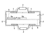
図1は、本発明の実施の形態1の光学部品に対する表裏面同時成膜を行う連続成膜装置の成膜室1を示す概略断面図であり、図2は基板ホルダー9の平面図、図3は基板ホルダー9における2個の光学部品である凹レンズ12、13が保持される基板室10の部分拡大断面図である。本実施の形態1の連続成膜装置は、上下にスパッタリングターゲット2、3を備えたスパッタリング装置として構成されている。
【0028】
即ち、前記成膜室1には、室内上方に配置されたスパッタリングターゲット2と、室内下方に配置されたスパッタリングターゲット3とが配置されている。
【0029】
前記成膜室1には、それぞれ前記スパッタリングターゲット2、3と前記基板ホルダー9との間にの位置にあり、成膜時には前記スパッタリングターゲット2、3と前記基板ホルダー9の間を塞がぬ位置(開位置)に移動し、非成膜時には前記スパッタリングターゲット2、3と前記基板ホルダー9の間を塞ぐ位置(閉位置)に移動するシャッター4、5を配置している。
【0030】
さらに、前記成膜室1には、図示せぬ前室と前記成膜室1とを区切るゲートバルブ6と、図示せぬ後室と前記成膜室1とを区切るゲートバルブ7とを設けている。
【0031】
また、前記成膜室1には、前記基板ホルダー9の移動のため、2本のコンベア状の基板ホルダー移動機構8を備えている。
【0032】
前記基板ホルダー移動機構8は、前記スパッタリングターゲット2、3と、基板ホルダー9の円形孔状の18個の基板室10との間を塞がない位置に2本平行に配置されている。
【0033】
ここで、前記基板ホルダー9は、図2に示す両端部の一対のすべり止め11によって前記基板ホルダー移動機構8と係合して成膜室1の中を図1に示す矢印a方向に移動可能となっている。
【0034】
前記基板ホルダー9の基板室10には、光学薄膜の成膜領域を上方に向けた光学部品である第一の凹レンズ12と、成膜領域を下方に向けた光学部品である第二の凹レンズ13とが保持される。
【0035】
前記基板室10は、図3に示すように、前記第一の凹レンズ12の成膜領域側から前記第一の凹レンズ12を保持する第一の基板保持具14と、前記第二の凹レンズ13の成膜領域側から前記第二の凹レンズ13を保持する第二の基板保持具15と、前記第一の凹レンズ12と前記第二の凹レンズ13を成膜領域の反対側から各々保持する第三の基板保持具16とから形成される。
【0036】
これら第一乃至第三の基板保持具14乃至16は、ネジ17により一体化される。ネジ17は、図4に示すように、ネジ頭部17aと、ネジ山部17bと、ネジ首部17cとからなり、前記ネジ首都17cは前記ネジ山部17bよりも細くなっている。前記第一、第二の基板保持具14,15には、前記ネジ山部17bに合致するネジ穴が設けられ、前記第三の基板保持具16には、前記ネジ山部17bを容易に貫通できる大ききの穴が設けられている。前記ネジ17は、前記第二の基板保持具15に予めワッシャー18とともに取り付けられている。
【0037】
即ち、基板ホルダー9は、それぞれ同じ大きさの長方形形状を持つ、前記第一の基板保持具14と、前記第二の基板保持具15と、前記第三の基板保持具16とにより主要な構成をなし、さらに、両端部の配置する一対のすべり止め11により、前記第一の基板保持具14と、前記第二の基板保持具15と、前記第三の基板保持具16とが一体化されて構成される。
【0038】
(作用)
以下に本実施の形態1の基板ホルダー9を使用した第一の凹レンズ12、第二の凹レンズ13に対する光学薄膜の成膜方法について図5乃至図8をも参照して説明する。
【0039】
図5に示すように、前記第一の基板保持具14の基板室10を形成する円形孔の部分に設けた受溝部14a上に18個の既に洗浄された凹レンズ12の成膜領域(成膜面)側を載せ、次に、図5に示すように、この第一の基板保持具14により保持された18個の凹レンズ12の成膜領域側とは反対側から第三の基板保持具16の基板室10を形成する18個の円形孔の部分に設けた円形の突条部16aの下面側を載せて18個の凹レンズ12を挟み込む。
【0040】
次に、図7に示すように、第三の基板保持具16の基板室10を形成する18個の円形孔の部分の突条部16aの上面側に、18個の既に洗浄された凹レンズ13の成膜領域側とは反対側の領域を各々載せる。
【0041】
次に、図8に示すように、第三の基板保持具16上の18個の凹レンズ13の成膜領域側に、第二の基板保持具15の基板室10を形成する円形孔の部分に設けた受溝部15aを各々被せて18個の凹レンズ13を挟み込む。
【0042】
この後、ネジ17を図示しないネジ止め具(ドライバー)により回転、固定することで、第一乃至第三の基板保持具14、15、16の両端部を押さえ込み、一体化する。
【0043】
次に、18個ずつの凹レンズ12、13を保持した前記基板ホルダー9を、図示せぬ連続成膜装置の排気室にセットし、図示せぬ排気装置により排気を開始する。
【0044】
その後、排気室の真空度が一定よりも良い値を示したところで、図示せぬ連続成膜装置の第一成膜(処理)室との間に設けられたゲートバルブが開き、前記基板ホルダー9は前記図示せぬ連続成膜装置の図示せぬ第一成膜室に送られる。
【0045】
ここで、図示せぬ連続成膜装置の前記成膜室1を含む各成膜室は、図示せぬ排気装置によりあらかじめ一定以上の真空度に排気されている。
【0046】
連続成膜装置の前記成膜室1の前段に置かれた図示せぬ各成膜室においてそれぞれの処理を施された後、前記基板ホルダー9は前記成膜室1へ前記ゲートバルブ6を経て送り込まれる。
【0047】
前記基板ホルダー9が前記成膜室1に送られた後、図示せぬガス導入機構によりスパッタガスが導入され、成膜室1内は0.4Paの一定圧に保たれる。ここで、前記スパッタリングターゲット2、3に図示せぬ電力供給装置により電力を供給し、前記スパッタリングターゲット2、3の上にプラズマを生成する。
【0048】
プラズマ生成時点においては、前記シャッター4、5は閉位置にあるが、プラズマが生成されて10秒後にこれは開位置に移動する。
【0049】
前記シャッター4、5が開位置にきたら、前記基板ホルダー9は前記基板ホルダー移動機構8により位置9aから位置9bに向かって移動を開始する。
【0050】
前記凹レンズ12、13の各成膜領域には、前記基板ホルダー9の移動に伴って、各々光学薄膜が形成される。
【0051】
即ち、前記上方に成膜領域を持つ凹レンズ12への成膜は、前記成膜室1の上方に配置されたスパッタリングターゲット2により行われ、前記下方に成膜領域を持つ凹レンズ13への成膜は、前記成膜室1の下方に配置されたスパッタリングターゲット3により行われる。
【0052】
ここで、基板ホルダー9の移動中での成膜により、各凹レンズ12、13の膜厚が所定の値になる。
【0053】
所定の膜厚の光学薄膜の形成が完了すると、図示せぬ電力供給装置による電力の供給が断たれ、プラズマが消滅する。同時に図示せぬガス導入機構によるガスの導入も停止し、前記シャッター4、5も閉位置へ移動する。
【0054】
次に、前記成膜室1のゲートバルブ7が開き、前記基板ホルダー9は、成膜室1から図示せぬ後室へ搬出される。
【0055】
このようにして、光学部品として同径の凹レンズ12、13への成膜を行うものであるが、上述した基板ホルダー9と同様の構造を有する基板ホルダーを使用し、かつ、同様の製造工程によって、径や形状の異なるレンズや、形状の異なるプリズム等、片面しか成膜の必要ない他の光学部品に対しても、各々成膜が必要な片面ずつの成膜を通常の2倍の充填率をもっ同時に行うことができる。
【0056】
本実施の形態1における、前記凹レンズ12を前記第一の基板保持具14と、前記第三の基板保持具16とに挟み込む工程の作業順序は、先に前記第一の基板保持具14を置き、その上に凹レンズ12、次に前記第三の基板保持具16を置くとしている。この作業順序は、先に前記第三の基板保持具16を置き、その上に凹レンズ12、次に前記第一の基板保持具14を置くとしても、本実施の形態の効果になんら影響がない。
【0057】
また、本実施の形態1において、第一乃至第三の基板保持具14乃至16を一体的に保持する押さえ具として機能したネジ17は、予め第一の基板保持具14に取り付けられ、一体化されていたが、前記ネジ17が別に用意され、後から取り付けられたとしても本実施の形態1の効果になんら影響がない。
【0058】
(効果)
本実施の形態1によれば、各々片面しか成膜の必要ない光学部品である凹レンズ12、13に対して、前記成膜室1における成膜工程によって通常の2倍の充填率で各々の片面に対して同時に成膜を行うことができ、高い生産性を得ることができる。
【0059】
(実施の形態2)
(構成)
以下に本発明の実施の形態2の構成を、図9、図10、図11を参照して説明する。
【0060】
図9はバッチ式成膜装置(真空蒸着装置)の成膜室21を示すものである。また図10は、略三角形状に形成され前記バッチ式成膜装置の基板反転機構に合致して、前記成膜室21内で反転が可能な反転パレット(基板ホルダー)26を示す平面図であり、図11は前記反転パレット26の基板室30を示す拡大断面図である。
【0061】
また、前記反転パレット26は、実施の形態1の第一乃至第三の基板保持具14、15、16と同様、受溝部34aを有する第一の基板保持具34、受溝部35aを有する第二の基板保持具35及び突条部36aを有する第三の基板保持具36を備え、これら第一乃至第三の基板保持具34、35、36により31個の基板室30を形成している。
【0062】
そして、図11に示すように、前記各基板室30により、成膜後接合され、一つの接合レンズとなる一組ずつの凹レンズ31、凸レンズ32を、凹レンズ31の成膜領域が下側、凸レンズ32の成膜領域が上側となるようにして挟み込み状態で保持するようになっつている。
【0063】
即ち、前記反転パレット26は、基板室30において、前記凹レンズ31の成膜領域側からこの凹レンズ31を保持する第一の基板保持具34と、前記凸レンズ32の成膜領域側からこの凸レンズ32を保持する第二の基板保持具35と、前記凹レンズ31と前記凸レンズ32を成膜領域の反対側から保持する第三の基板保持具36とを具備している。
【0064】
前記凹レンズ31と、前記凸レンズ32とは、屈折率の異なる光学ガラスを素材としている。
【0065】
前記成膜室21は、下方に配置された電子銃型蒸着源22、下方に配置されたエンドホール型イオンガン23、上方に配置された前記反転パレット26が装着され、その中で前記反転パレット28の反転動作が可能なドーム枠24、前記電子銃型蒸着源22に付属しており、成膜時には前記電子銃型蒸着源22と前記ドーム枠24に装着された反転パレット26の間を塞がぬ位置(開位置)、非成膜時には前記電子銃型蒸着源22と前記ドーム枠24に装着された反転パレット26の間を塞ぐ位置(閉位置)とるシャッター25、及び、反転パレット26を反転させる図示せぬ基板反転機構を具備している。
【0066】
前記電子銃型蒸着源22は、複数の蒸着物質を蒸着するために、図示せぬ材料交換機構を具備している。
【0067】
前記反転パレット26は、この反転パレット26が反転する時にその回転軸となる図9に示す反転軸27、28を介して、前記ドーム枠24に装着される。
【0068】
(作用)
以下に本実施の形態2における凹レンズ31、凸レンズ32への成膜方法について説明する。
【0069】
実施の形態1の場合と同様にして、前記第一の基板保持具34と前記第三の基板保持具36の間に31個の既に洗浄された凹レンズ31を挟み込み、更に、第二の基板保持具35と第三の基板保持具36の間に31個の既に洗浄された凸レンズ32を挟み込み、前記図示せぬ押さえ手段によりこれらを一体化して、反転パレット26とする。
【0070】
この反転パレット26を、前記凹レンズ31の成膜領域(下面)が電子銃型蒸着源22に対面する配置で前記成膜室21の前記ドーム枠24に装着し、図示せぬ排気装置により排気を開始する。
【0071】
その後、排気室の真空度が一定よりも良い値を示した後、前記イオンガン23を動作させて、成膜対象である前記凹レンズ31に向けて、図示せぬイオンビームを放出する。
【0072】
更に、前記シャッター5が閉位置にある状態で前記図示せぬ材料交換機構により蒸着材料22aの選択が行われた後、前記電子銃型蒸着源22を動作させて蒸着材料22aを加熱する。前記電子銃型蒸着源22が安定したところで前記シャッター25を開位置として前記凹レンズ31に対する蒸着を開始する。
【0073】
ここで、前記図示せぬイオンビームの働きにより、前記凹レンズ31の表面に形成される光学薄膜は、十分な光学特性、機械的強度を持った薄膜となる。
【0074】
前記凹レンズ31の成膜領域表面に所定の光学薄膜の形成が完了して、前記シャッター5が閉位置をとった後に、前記電子銃型蒸着源22は一時動作を止めて、図示せぬ材料交換機構により次層の蒸着材料が選択される。
【0075】
このようなプロセスにより必要な層数の光学薄膜を形成した後、前記イオンガン3の動作を停止させ、図示せぬ基板反転機構により、反転パレット26を表裏反転する。反転パレット26の表裏反転により、成膜対象である凸レンズ32の成膜領域が電子銃型蒸着源22に向く。
【0076】
この後、前記と同様のプロセスにより、前記凸レンズ32の成膜領域にも、所定の光学薄膜を形成する。
【0077】
本実施の形態2では、光学部品として一つの接合レンズを構成する一組の凹レンズ31、凸レンズ32の成膜を行う場合について説明したが、反転パレット26と同様の構造の基板ホルダー、及び、製造工程によって、径や形状の異なるレンズや、形状の異なるプリズム等、他の片面しか成膜の必要ない光学部品に対しても、本実施の形態2の場合と同様にして成膜が可能である。
【0078】
また、本実施の形態2では、十分な光学特性、機械的強度を持った薄膜を得るために、エンドホール型のイオンガン23を利用したが、十分な光学特性、機械的強度を持った薄膜を得るには、この他、イオンガン23を使用する代わりに加熱を行い基板を予め高い温度に安定させる等して成膜を行っても本実施の形態2の効果に変わりはない。
【0079】
更に、成膜基板がプラスチックで、イオンガンや加熱、又はそれに代替えする手段を用いずとも所望の特性をもつ薄膜が得られる場合には、同様の成膜装置で、イオンガンや加熱、又はそれに代替する手段を用いずに成膜を行い、本実施の形態2と同様の効果を得ることができる。
【0080】
(効果)
本実施の形態2によれば、片面しか成膜の必要ない光学部品においても、片面ずつ順次成膜を行う両面成膜装置を使用して、同バッチで通常の2倍の充填率をもって成膜領域が表裏に配置された一対ずつの光学部品に対する成膜を順次に行うことができ、高い生産性を得ることができる。
【0081】
特に、一つの接合レンズを構成する一組の凹レンズ31、凸レンズ32を対象としたことで、その生産数量は同一となることから、接合レンズ生産の編成がし易いという利点と、その径が同一であるため成膜室21内への充填率が高くなり、より高い効果を得ることができる。
【0082】
(実施の形態3)
(構成)
本発明の実施の形態3の構成は、蒸着装置が、排気室、成膜室、ベント室の3槽からなる連続式の蒸着装置であること、反転パレット用の反転枠を排気室から成膜室、成膜室からベント室へ移送するための移送機構が具備されていること、成膜室にはイオンガンが無く、これに替わり、排気室、成膜室に反転パレットを加熱するためのヒータが備え付けてあることを除き、上述した実施の形態2の場合と同様である。
【0083】
前記排気室に備え付けられたヒータは、反転パレットの基板室を上下から効率よく加熱することのできるように、排気室の上下に設けられており、前記成膜室に備え付けられたヒータは、成膜室上方に備え付けられている。また、前記成膜室は、成膜を行うのに必要な真空度となるように予め排気されている。
【0084】
(作用)
実施の形態2と同様にして第一の光学部品、第二の光学部品を保持した反転パレットを反転枠に装着した状態で前記排気室に投入し、排気を始める。
【0085】
前記反転枠に装着された反転パレット及びこれに保持される各光学部品は、排気工程中に、前記排気室に設けられたヒータにより、第一の光学部品及び第二の光学部品共に効率よく加熱され、前記排気室が前記成膜室の真空度と同等程度の真空度にまで排気されるまでに、250℃程度の温度で安定する。
【0086】
前記排気室の真空度が、前記成膜室の真空度と同等程度の真空度にまで排気されると、前記移送機構により、反転粋が成膜室に移送される。
【0087】
反転枠が成膜室に移送された後、第一の光学部品及び第二の光学部品は前記成膜室上方に設けられたヒータにより、加熱が継続され、光学部品の温度は250℃程度で安定される。
【0088】
その後、実施の形態2と同様のプロセスにより、前記第一の光学部品、前記第二の光学部品それぞれの成膜領域に所望の光学薄膜が形成され、光学薄膜の形成が終了したら、さらに前記反転枠は前記移送機構により前記ベント室に移送され、反転パレットの冷却、大気解放がなされ、前記反転枠に装着された前記反転パレット、及び、これに保持される第一の光学部品、第二の光学部品が取り出される。
【0089】
(効果)
本実施の形態3によれば、片面しか成膜の必要ない光学部品においても、両面成膜装置によって同バッチに通常の2倍の充填率で表裏に配置された一組ずつの光学部品に対する成膜を順次に行うことができ、高い生産性を得ることができる。
【0090】
特に、光学部品として、一つの接合レンズを構成する一組のレンズを対象とすれば、その生産数量は同一となることから接合レンズの生産の編成がしやすいという利点と、その径が同一であることから成膜室内における充填率が高くなり、より高い効果を得ることができる。
【0091】
また、成膜前に第一の光学部品、第二の光学部品ともに直接に加熱できる機能を持つ蒸着装置を用いたことで、両方の光学部品が短時間で同程度の温度になるように安定して加熱でき、安定した生産性をえることができる。
【0092】
(実施の形態4)
(構成)
次に、本発明の実施の形態4について図12を参照して説明する。
本実施の形態4における基板ホルダー41は、図12に示すように、基板室50において、第一の自由曲面プリズム52の成膜領域側が外側(図12において下側)となる状態で受溝部44aにて保持する第一の基板保持具44と、第二の自由曲面プリズム53の成膜領域側を外側(図11において上側)となる状態で受溝部45aにて保持する第二の基板保持具45と、第一の基板保持具44、第二の基板保持具45の間に介在して第一の自由曲面プリズム52、第二の自由曲面プリズム53の各成膜領域とは反対側の一端を各々保持する分離構造の第三の基板保持具46a、46bと、第一の基板保持具44、第二の基板保持具45、第三の基板保持具46a、46bを一体化する図示しない押さえ手段とを具備している。
【0093】
(作用)
本実施の形態4において、各自由曲面プリズム52、53を、基板ホルダー41の基板室50に取り付る際、最初に第一の基板保持具44の受溝部44a上に第一の自由曲面プリズム52の成膜領域側を載せ、一方の第三の基板保持具46aに設けた突出片46cにより第一の自由曲面プリズム52の成膜領域とは反対側の一端を固定保持する。
【0094】
次に、前記第一の基板保持具44に第一の自由曲面プリズム52を固定した場合と同様に、第二の基板保持具45の受溝部45aにより第二の自由曲面プリズム53を載せ、第三の基板保持具46bに設けた突出片46dにより第二の自由曲面プリズム53の成膜領域とは反対側の一端を固定保持する。
【0095】
このようにして第一の基板保持具44、第二の基板保持具45上にそれぞれ第一の自由曲面プリズム52、第二の自由曲面プリズム53が固定保持された後、図11に示すように第一の自由曲面プリズム52、第二の自由曲面プリズム53の各成膜領域と反対側の領域が対向するようにしてこれらを突き合わせて、図示しない押さえ手段により一体化することで、図12に示すような基板室50の構造とするものである。
【0096】
本実施の形態4における基板室50の構成は、既述した実施の形態1乃至3のいずれの場合にも適用でき、その場合の作用は光学部品の保持方法を除き、各々実施の形態1乃至3の場合と同様である。
【0097】
(効果)
本実施の形態4によれば、自由曲面プリズムのような光学部品の場合においても、実施の形態1乃至3に示した場合と同様の効果を得ることができる。また、自由曲面プリズムの固定保持に用いた第三の基板保持具46a、46bが一体をなさず分離した構造でも、同様の効果を得ることができる。
【0098】
以上説明した本発明によれば、以下の構成を付記することができる。
【0099】
(付記)接合レンズを構成する接合前の第一のレンズの成膜領域側から第一の基板保持具により、第一のレンズの成膜領域反対側から第三の基板保持具により前記第一のレンズを挟むことでこの第一のレンズを保持するとともにその光学機能面に対して成膜領域を決める工程と、第三の基板保持具上に接合レンズを構成する接合前の第二のレンズを置く工程と、第三の基板保持具により支持された前記第二のレンズの成膜領域側を第二の基板保持具により挟み込み、前記第一乃至第三の基板保持具を一体化する工程と、第一乃至第三の基板保持具により保持された前記両レンズの各成膜領域に光学薄膜を同時に又は順に成膜する工程とを含むことを特徴とする光学部品の製造方法。
【0100】
この光学部品の製造方法によれば、接合前の各レンズが、最終的に接合され一つの接合レンズとなる一組のレンズである場合、その生産数量は同一となることから生産の編成がし易いという利点と、一般にその径が同一か略同じであるため成膜室内における充填率を上げ易いという利点があり、特に効果が高くなる。
【0101】
【発明の効果】
請求項1、3、4記載の発明によれば、複数の蒸着源に複数の成膜面が対向するような成膜装置においても、また、前記成膜基板自体を反転させる成膜装置においても、各々利用することができ、これにより、光学部品の広範な生産形態において生産性向上の効果を得ることができる基板ホルダーを提供することができる。
【0102】
請求項2記載の発明によれば、固定保持した2個の光学部品の成膜が必要な各成膜領域に光学薄膜を順に形成する場合において、容易に生産性向上の効果を得ることができる基板ホルダーを提供することができる。
【0103】
請求項5、6記載の発明によれば、前記請求項1記載の発明の基板ホルダーを用いて、又は、前記請求項5記載の発明の基板ホルダーを用いて、前記第一、第二の光学部品の各成膜領域に光学薄膜を同時に又は順に成膜するものであり、第一、第二の光学部品を恰も一つの光学部品のような状態で扱い、各成膜領域に対する成膜を行うことができ、これにより、光学部品に対する成膜を行う際の効率向上、さらには生産性向上を図ることができる光学部品の製造方法を提供できる。
【図面の簡単な説明】
【図1】本発明の実施の形態1の連続成膜装置の成膜室を示す概略断面図である。
【図2】本発明の実施の形態1の基板ホルダーの平面図である。
【図3】本発明の実施の形態1の基板ホルダーにおける2個の光学部品である凹レンズ、凸レンズが保持される基板室の部分拡大断面図である。
【図4】本発明の実施の形態1の第一乃至第三の基板保持具及びこれらを一体化するネジの構造を示す部分断面図である。
【図5】本発明の実施の形態1の基板ホルダーにより凹レンズを保持する工程を示す部分拡大断面図である。
【図6】本発明の実施の形態1の基板ホルダーにより凹レンズを挟み込む工程を示す部分拡大断面図である。
【図7】本発明の実施の形態1の基板ホルダーにより凸レンズを保持する工程を示す部分拡大断面図である。
【図8】本発明の実施の形態1の基板ホルダーにより凸レンズを挟み込む工程を示す部分拡大断面図である。
【図9】本発明の実施の形態2の成膜室を示す概略構成図である。
【図10】本発明の実施の形態2の反転パレットの平面図である。
【図11】本発明の実施の形態2の反転パレットにより2個の光学部品である凹レンズ、凸レンズが保持される基板室の部分拡大断面図である。
【図12】本発明の実施の形態4の基板室の部分拡大断面図である。
【符号の説明】
1 成膜室
2 スパッタリングターゲット
3 スパッタリングターゲット
4 シャッター
6 ゲートバルブ
7 ゲートバルブ
8 基板ホルダー移動機構
9 基板ホルダー
10 基板室
11 すべり止め
12 凹レンズ
13 凹レンズ
14 第一の基板保持具
15 第二の基板保持具
16 第三の基板保持具
17 ネジ
18 ワッシャー
21 成膜室
22 電子銃型蒸着源
23 イオンガン
24 ドーム枠
25 シャッター
26 反転パレット
27 反転軸
30 基板室
31 凹レンズ
32 凸レンズ
34 第一の基板保持具
35 第二の基板保持具
35 第三の基板保持具[0001]
BACKGROUND OF THE INVENTION
The present invention relates to a substrate holder used for manufacturing an optical component and an optical component manufacturing method using the substrate holder.
[0002]
[Prior art]
Conventionally, optical parts such as lenses and prisms often have an optical thin film formed on the surface thereof. In particular, the lens often has an antireflection film formed on both surfaces of the lens in order to ensure the transmittance.
[0003]
By the way, when an optical film such as an antireflection film is formed on the surface of the optical component, film formation is performed in a vacuum atmosphere such that vacuum deposition is a representative example in order to satisfy the high required performance. In order to obtain the vacuum atmosphere, it is usually necessary to perform evacuation for about 1 hour or more, and the evacuation time occupies much of the time necessary for forming the optical film.
[0004]
The time required for this evacuation occupies a large part of the manufacturing tact time when an optical component having an antireflection film formed on both surfaces is to be manufactured.
[0005]
As a method for reducing the time loss due to the long evacuation time and increasing the production efficiency, film formation on both sides of the same batch (one evacuation) disclosed in, for example, Japanese Utility Model Publication No. 6-73156. There is a method using an inverted palette to perform the above.
[0006]
According to this method, the cost of the apparatus increases because a mechanism for performing double-sided film formation is added to the film forming apparatus, but the evacuation that requires a long time only needs to be performed once, and the production efficiency is reliably increased. Can do.
[0007]
[Problems to be solved by the invention]
However, in the method using the reversal palette disclosed in Japanese Utility Model Laid-Open No. 6-73156, for example, in an optical component that requires film formation on only one side, such as a pre-junction lens constituting a cemented lens, There is a problem that the benefits of double-sided film formation in the film apparatus cannot be obtained and productivity cannot be increased.
[0008]
The present invention solves the above problems, and provides a substrate holder that can contribute to productivity improvement even in the case of film formation of an optical component that needs to be formed on only one side, and the substrate holder An object of the present invention is to provide a method of manufacturing an optical component that can improve the production efficiency by using the above.
[0009]
[Means for Solving the Problems]
The invention described in claim 1Having a circular hole part,A first substrate holder that determines the film formation region relative to the optical functional surface of the first optical component and holds the first optical component from the film formation region side;Having a circular hole part,A second substrate holder for determining the film formation region with respect to the optical functional surface of the second optical component and holding the second optical component from the film formation region side;Having a circular hole part,A third intervening between the first substrate holder and the second substrate holder and holding the first optical component and the second optical component from the opposite side of the film formation region, respectively. A substrate holder and holding means for integrally holding the first to third substrate holders.And between the receiving groove portion provided in the circular hole portion of the first substrate holder and the protruding portion provided in the circular hole portion of the third substrate holder. One optical component can be held, a receiving groove provided in the circular hole portion of the second substrate holder, and a protrusion provided in the circular hole portion of the third substrate holder The second optical component can be held between the optical component and the optical component when the optical thin film is formed on the optical functional surface of the optical component by the film forming apparatus.Board holderIt is.
[0010]
The operation of the invention of claim 1 will be described. When film formation is performed on multiple surfaces of an optical component using a normal film formation apparatus that does not have a mechanism for performing simultaneous film formation on multiple surfaces, It is necessary to repeat a preparation process such as setting of a film formation substrate, a vacuum exhaust process, a film formation process, and a process for returning the vacuum to atmospheric pressure.
[0011]
On the other hand, when a film forming apparatus having a mechanism for simultaneously forming a plurality of surfaces is used, the above process does not need to be repeated except for the film forming process, so that the manufacturing tact time of the optical component can be shortened.
[0012]
As a method for performing simultaneous film formation on a plurality of surfaces as described above, an apparatus in which a plurality of film formation surfaces are opposed to a plurality of film formation sources (for example, two sputtering targets are provided at opposed positions and a film is formed between them. There are a method using a sputtering apparatus in which a substrate is disposed, and a method for inverting the film formation substrate itself (for example, using an inversion pallet as disclosed in Japanese Utility Model Publication No. 6-73166).
[0013]
According to the first aspect of the present invention, two optical components that only require film formation from one side are provided in the same manner by providing a third substrate holder between the first and second substrate holders. It can be mounted on a substrate holder and can be handled like an optical component having a plurality of film-forming surfaces.
[0014]
That is, it is possible to perform film formation of optical components that require film formation only from one side at the same time, or at a filling rate that is twice as high. Even in the case of optical components that only require film deposition from one side, which could not benefit from improved production efficiency due to simultaneous film deposition on multiple surfaces, it is equivalent to the case of optical components by simultaneous film deposition on multiple surfaces The effect of improving productivity can be obtained.
[0015]
That is, according to the substrate holder of the first aspect of the present invention, even in a film forming apparatus in which a plurality of film forming surfaces face the plurality of vapor deposition sources, the film forming apparatus for inverting the film forming substrate itself Can also be used, and thereby the effect of improving productivity can be obtained in a wide range of production forms of optical components.
[0016]
According to a second aspect of the present invention, in the substrate holder according to the first aspect, the substrate holder includes a front / back reversing shaft that can be supported by the substrate reversing mechanism provided in the film forming apparatus so that the front / back can be reversed. It is characterized by.
[0017]
According to the second aspect of the present invention, the substrate according to the first aspect of the present invention can be used when forming the optical thin film on the surface of the optical component relatively, and the substrate that reverses the film formation substrate that is often used in practice. Applicable to a film forming apparatus having a reversing mechanism, thereby improving productivity when forming an optical thin film in order in each film forming region of two optical components held by the substrate holder. The effect of can be obtained.
[0018]
The invention described in claim 3A first substrate holder having a first receiving groove, a second substrate holder having a second receiving groove, and disposed between the first substrate holder and the second substrate holder; A third substrate holder and pressing means for integrally holding the first to third substrate holders, and the first opening is formed from the surface side of the first substrate holder. The opening is formed so that the opening diameter gradually decreases toward the third substrate holder, and the first recess has the first receiving groove and faces the third substrate holder. The back surface of the first substrate holder is formed wider than the minimum opening surface of the first opening, and the second opening is formed from the back surface side of the second substrate holder to the third substrate. The opening is formed so that the opening diameter gradually decreases toward the holder, the second recess has the second receiving groove, and the third substrate holder is formed. Formed on the surface of the second substrate holder facing the tool wider than the minimum opening surface of the second opening, and the minimum opening diameter of the first opening is the first substrate The diameter coincides with the film forming region formed on the optical functional surface of the optical component held by the holder and the third substrate holder, and the minimum opening diameter of the second opening is the second substrate holding The diameter coincides with the film forming region formed on the optical functional surface of the optical component held by the fixture and the third substrate holder, and the third substrate holder has a protrusion, and the protrusion Is formed of a third opening and a third recess, and the third opening is formed to penetrate from the surface on the third substrate holder side to the back surface, and the third recess is It is formed wider on the front and back surfaces of the third substrate holder than the opening surface of the third opening.It is characterized by that.
[0019]
According to the invention described in
Claim 4In the invention described, the first free-form surface prism is held from the film formation region side of the first free-form surface prism, the first substrate holder having the first opening, and the second free-form surface prism A second substrate holder holding the second free-form curved prism from the film formation region side and having a second opening, and interposed between the first substrate holder and the second substrate holder A third substrate holder having a third opening and a separation structure for holding the first free-form surface prism and the second free-form surface prism at one end opposite to the film formation region, respectively. Pressing means for integrally holding the first to third substrate holders, wherein the first substrate holder is provided with a receiving groove provided in a portion of the first opening, The first free curved surface plug is interposed between the protruding piece provided in the third opening of the third substrate holder. A receiving groove portion provided in the second opening portion of the second substrate holder, and a protruding piece provided in the third opening portion of the third substrate holder. The substrate holder for holding the optical component when the optical thin film is formed on the optical functional surface of the optical component by a film forming apparatus, wherein the second free-form curved prism can be held between It is.
Claim 5According to the invention described in claim 1, using the substrate holder according to
And at least one of the first optical component and the second optical component has a convex shape on the opposite side of the film formation region.
Claim 6The described inventionClaim 4Using the substrate holder described above, the receiving groove portion of the first substrate holder from the film formation region side of the first free-form surface prism, and the film formation region of the first free-form surface prism from the opposite side of the film formation region A step of holding the first free-form curved prism by sandwiching the first free-form curved prism by the protruding piece of the third substrate holder, and determining the film formation region with respect to the optical function surface And a step of placing the second free-form curved prism on the protruding piece of the third substrate holder with the region opposite to the film formation region facing down, and a second supported by the third substrate holder A step of sandwiching the film-forming region of the second free-form curved prism by the receiving groove of the second substrate holder, and integrating the first to third substrate holders; and the first to third substrate holders Said first held by a tool, Second optical thin film on each deposition region of the free-form surface prisms simultaneously, or a method of manufacturing an optical component made of a free curved surface prism, characterized in that in order includes a step of forming, the.
[0020]
In each of these inventions, there is an effect when holding optical components one by one as a substrate holder, but as in the conventional example (Japanese Utility Model Publication No. 6-73166), a large number of substrate chambers are provided for each front and back. When a large number of optical components are held at the same time, the effect of improving productivity is further increased.
[0021]
Also, if the first optical component and the second optical component that are combined front and back are the same, or if their diameters are the same, it is easy to increase the filling rate as in the case of a cemented lens. Advantages arise and are particularly effective.
[0022]
In addition, if heating is required for film formation and the optical component is particularly large, a lot of time is required for the heating process and the cooling process. In such a case, the substrate holder and the optical component of the present invention are used. The effect by application of a manufacturing method becomes high.
[0023]
Specifically, when heating is required for the film formation and the optical component is particularly large, the temperature of the optical component to be formed is set to a high temperature of 200 ° C. or higher in the heating step performed in parallel during the exhaust stroke. It needs to stabilize and takes a considerable amount of time.
[0024]
Further, after the film formation step, before the process of returning the vacuum to the atmospheric pressure, the optical component after the film formation must be cooled to a temperature below a certain level, the optical in the step of returning the vacuum to the atmospheric pressure. Since the optical component may be cracked due to rapid cooling of the component, the cooling time also requires a considerable amount of time. Therefore, a high effect can be obtained by improving the filling rate of the optical component according to the present invention.
[0025]
Further, the third substrate holder used in the present invention is configured such that the first optical component and the second optical component are paired with the first substrate holder and the second substrate holder, respectively. Since it is to hold, this is not limited to one, and if necessary, it may take two or more separate forms, and even with such a configuration, the same effect can be obtained. . In addition, the pressing means for integrally holding the first to third substrate holders used in the present invention is a case where a single body is formed as a pressing member like a clip, or the first to third substrate holders. They may be integrated and provided as part of them. In either case, the pressing means can obtain the same effect as long as it has a function of holding the first to third substrate holders integrally.
[0026]
DETAILED DESCRIPTION OF THE INVENTION
Hereinafter, embodiments of the present invention will be described in detail.
[0027]
(Embodiment 1)
(Constitution)
FIG. 1 is a schematic cross-sectional view showing a film forming chamber 1 of a continuous film forming apparatus that performs simultaneous film formation on the front and back surfaces of the optical component according to Embodiment 1 of the present invention. FIG. 3 is a partially enlarged sectional view of the
[0028]
That is, in the film forming chamber 1, a
[0029]
The film formation chamber 1 is located between the sputtering
[0030]
Further, the film formation chamber 1 is provided with a
[0031]
Further, the film forming chamber 1 is provided with two conveyor-like substrate
[0032]
Two substrate
[0033]
Here, the
[0034]
In the
[0035]
As shown in FIG. 3, the
[0036]
The first to
[0037]
That is, the
[0038]
(Function)
Hereinafter, a method for forming an optical thin film on the first
[0039]
As shown in FIG. 5, film formation regions (film formations) of 18 already washed
[0040]
Next, as shown in FIG. 7, 18 already cleaned
[0041]
Next, as shown in FIG. 8, on the side of the film formation region of the 18
[0042]
Thereafter, the
[0043]
Next, the
[0044]
Thereafter, when the degree of vacuum in the exhaust chamber shows a value better than a certain value, a gate valve provided between the first film forming (processing) chamber of a continuous film forming apparatus (not shown) is opened, and the
[0045]
Here, each film forming chamber including the film forming chamber 1 of the continuous film forming apparatus (not shown) is evacuated to a certain degree of vacuum in advance by an exhaust apparatus (not shown).
[0046]
After the respective processing is performed in each film forming chamber (not shown) placed in front of the film forming chamber 1 of the continuous film forming apparatus, the
[0047]
After the
[0048]
At the time of plasma generation, the
[0049]
When the
[0050]
An optical thin film is formed in each film formation region of the
[0051]
That is, the film formation on the
[0052]
Here, the film thickness of each
[0053]
When the formation of the optical thin film having a predetermined thickness is completed, the power supply by a power supply device (not shown) is cut off, and the plasma disappears. At the same time, gas introduction by a gas introduction mechanism (not shown) is stopped, and the
[0054]
Next, the gate valve 7 of the film forming chamber 1 is opened, and the
[0055]
In this way, film formation is performed on the
[0056]
In the first embodiment, the work order of the step of sandwiching the
[0057]
In the first embodiment, the
[0058]
(effect)
According to the first embodiment, with respect to the
[0059]
(Embodiment 2)
(Constitution)
Hereinafter, the configuration of the second embodiment of the present invention will be described with reference to FIG. 9, FIG. 10, and FIG.
[0060]
FIG. 9 shows a
[0061]
The reversing
[0062]
Then, as shown in FIG. 11, a set of
[0063]
That is, the
[0064]
The
[0065]
The
[0066]
The electron gun-
[0067]
The reversing
[0068]
(Function)
The film forming method on the
[0069]
In the same manner as in the first embodiment, 31 already cleaned
[0070]
The
[0071]
Thereafter, after the degree of vacuum in the exhaust chamber shows a value better than a certain value, the
[0072]
Furthermore, after the
[0073]
Here, the optical thin film formed on the surface of the
[0074]
After the formation of a predetermined optical thin film on the surface of the film formation region of the
[0075]
After forming the required number of optical thin films by such a process, the operation of the
[0076]
Thereafter, a predetermined optical thin film is formed also in the film forming region of the
[0077]
In the second embodiment, the case where a pair of
[0078]
In the second embodiment, the end-hole
[0079]
Furthermore, if the film formation substrate is plastic and a thin film having the desired characteristics can be obtained without using an ion gun, heating, or alternative means, the same film forming apparatus can be used to replace the ion gun, heating, or the like. Film formation can be performed without using any means, and the same effect as in the second embodiment can be obtained.
[0080]
(effect)
According to the second embodiment, even in an optical component that needs to be formed on only one side, a double-sided film forming apparatus that sequentially forms films on each side is used to form a film with a filling rate twice that of a normal batch. Films can be sequentially formed on a pair of optical components whose regions are arranged on the front and back sides, and high productivity can be obtained.
[0081]
In particular, since the production quantity is the same by targeting a set of
[0082]
(Embodiment 3)
(Constitution)
The configuration of
[0083]
The heater provided in the exhaust chamber is provided above and below the exhaust chamber so that the substrate chamber of the reversal pallet can be efficiently heated from above and below. It is provided above the membrane chamber. In addition, the film formation chamber is evacuated in advance so as to obtain a degree of vacuum necessary for film formation.
[0084]
(Function)
In the same manner as in the second embodiment, the reverse pallet holding the first optical component and the second optical component is put into the exhaust chamber in a state where the reverse pallet is mounted on the reverse frame, and exhaust is started.
[0085]
The reversing pallet mounted on the reversing frame and the optical components held by the reversing frame are both efficiently heated by the heater provided in the exhaust chamber during the exhaust process. The evacuation chamber is stabilized at a temperature of about 250 ° C. until the evacuation chamber is evacuated to a degree of vacuum equivalent to that of the film formation chamber.
[0086]
When the degree of vacuum in the exhaust chamber is evacuated to a degree of vacuum equivalent to the degree of vacuum in the film formation chamber, the reverse mechanism is transferred to the film formation chamber by the transfer mechanism.
[0087]
After the reversal frame is transferred to the film forming chamber, the first optical component and the second optical component are continuously heated by the heater provided above the film forming chamber, and the temperature of the optical component is about 250 ° C. It is stabilized.
[0088]
Thereafter, a desired optical thin film is formed in the film formation region of each of the first optical component and the second optical component by the same process as in the second embodiment, and when the formation of the optical thin film is completed, the inversion is further performed. The frame is transferred to the vent chamber by the transfer mechanism, the reversing pallet is cooled and released to the atmosphere, the reversing pallet mounted on the reversing frame, and the first optical component held on the reversing pallet, the second The optical component is removed.
[0089]
(effect)
According to the third embodiment, even for an optical component that needs to be formed on only one side, a double-sided film forming apparatus forms a set of optical components arranged on the front and back in the same batch at twice the normal filling rate. Membranes can be sequentially formed, and high productivity can be obtained.
[0090]
In particular, if a set of lenses constituting one cemented lens is used as an optical component, the production quantity is the same, so the advantage is that it is easy to organize the production of the cemented lens, and the diameter is the same. For this reason, the filling rate in the film forming chamber is increased, and a higher effect can be obtained.
[0091]
In addition, by using a vapor deposition system that has the function of heating both the first and second optical components directly before film formation, both optical components can be stabilized at the same temperature in a short time. Can be heated and stable productivity can be obtained.
[0092]
(Embodiment 4)
(Constitution)
Next, a fourth embodiment of the present invention will be described with reference to FIG.
As shown in FIG. 12, the substrate holder 41 according to the fourth embodiment has a receiving
[0093]
(Function)
In the fourth embodiment, when the free-
[0094]
Next, as in the case where the first free-form
[0095]
After the first free-
[0096]
The configuration of the
[0097]
(effect)
According to the fourth embodiment, even in the case of an optical component such as a free-form curved prism, the same effects as those shown in the first to third embodiments can be obtained. Further, the same effect can be obtained even in a structure in which the
[0098]
According to the present invention described above, the following configurations can be added.
[0099]
(Supplementary note) The first substrate holder from the film formation region side of the first lens before the cemented lens constituting the cemented lens and the third substrate holder from the opposite side of the first lens film formation region to the first lens Holding the first lens by sandwiching the first lens and determining the film forming area with respect to the optical function surface, and the second lens before bonding constituting the bonded lens on the third substrate holder And the step of sandwiching the film formation region side of the second lens supported by the third substrate holder with the second substrate holder and integrating the first to third substrate holders And a method of forming an optical thin film simultaneously or sequentially on the film forming regions of the two lenses held by the first to third substrate holders.
[0100]
According to this method of manufacturing an optical component, when each lens before being joined is a set of lenses that are finally joined to become one joined lens, the production quantity is the same, so the production is organized. The advantage is that it is easy and the diameter is generally the same or substantially the same, so that there is an advantage that it is easy to increase the filling rate in the film forming chamber, and the effect is particularly high.
[0101]
【The invention's effect】
[0102]
According to the second aspect of the present invention, in the case where the optical thin film is sequentially formed in each film formation region where the film formation of the two optical components fixedly held is required, the effect of improving the productivity can be easily obtained. A substrate holder can be provided.
[0103]
[Brief description of the drawings]
FIG. 1 is a schematic sectional view showing a film forming chamber of a continuous film forming apparatus according to a first embodiment of the present invention.
FIG. 2 is a plan view of a substrate holder according to the first embodiment of the present invention.
FIG. 3 is a partial enlarged cross-sectional view of a substrate chamber in which a concave lens and a convex lens, which are two optical components, in the substrate holder according to the first embodiment of the present invention are held.
4 is a partial cross-sectional view showing the structure of first to third substrate holders according to Embodiment 1 of the present invention and a screw for integrating them. FIG.
FIG. 5 is a partially enlarged cross-sectional view showing a step of holding the concave lens by the substrate holder according to the first embodiment of the present invention.
FIG. 6 is a partially enlarged cross-sectional view showing a step of sandwiching the concave lens by the substrate holder according to the first embodiment of the present invention.
FIG. 7 is a partially enlarged cross-sectional view showing a process of holding the convex lens by the substrate holder according to the first embodiment of the present invention.
FIG. 8 is a partially enlarged cross-sectional view showing a step of sandwiching a convex lens by the substrate holder according to the first embodiment of the present invention.
FIG. 9 is a schematic configuration diagram showing a film forming chamber according to a second embodiment of the present invention.
FIG. 10 is a plan view of an inversion pallet according to
FIG. 11 is a partial enlarged cross-sectional view of a substrate chamber in which a concave lens and a convex lens, which are two optical components, are held by an inversion palette according to
FIG. 12 is a partial enlarged cross-sectional view of a substrate chamber according to Embodiment 4 of the present invention.
[Explanation of symbols]
1 Deposition chamber
2 Sputtering target
3 Sputtering target
4 Shutter
6 Gate valve
7 Gate valve
8 Substrate holder moving mechanism
9 Substrate holder
10 Substrate room
11 Anti-slip
12 Concave lens
13 Concave lens
14 First substrate holder
15 Second substrate holder
16 Third substrate holder
17 Screw
18 Washer
21 Deposition chamber
22 Electron gun type evaporation source
23 Ion Gun
24 Dome frame
25 Shutter
26 Reverse palette
27 Reverse axis
30 Substrate room
31 concave lens
32 Convex lens
34 First substrate holder
35 Second substrate holder
35 Third substrate holder
Claims (6)
円形孔の部分を有し、第二の光学部品の光学機能面に対して成膜領域を決め成膜領域側から前記第二の光学部品を保持する第二の基板保持具と、
円形孔の部分を有し、前記第一の基板保持具と前記第二の基板保持具の間に介在し、前記第一の光学部品と前記第二の光学部品とを各々成膜領域の反対領域側から保持する第三の基板保持具と、
前記第一乃至第三の基板保持具を一体的に保持する押さえ手段と、
を有し、
前記第一の基板保持具の前記円形孔の部分に設けられた受溝部と、前記第三の基板保持具の前記円形孔の部分に設けられた突条部との間に、前記第一の光学部品を保持可能であり、
前記第二の基板保持具の前記円形孔の部分に設けられた受溝部と、前記第三の基板保持具の前記円形孔の部分に設けられた突条部との間に、前記第二の光学部品を保持可能であることを特徴とし、
光学部品の光学機能面に成膜装置により光学薄膜を形成する際に、前記光学部品を保持する基板ホルダー。A first substrate holder having a circular hole portion, determining a film formation region with respect to the optical functional surface of the first optical component, and holding the first optical component from the film formation region side;
A second substrate holder having a circular hole portion, determining a film formation region with respect to the optical functional surface of the second optical component, and holding the second optical component from the film formation region side;
A circular hole portion is interposed between the first substrate holder and the second substrate holder, and the first optical component and the second optical component are respectively opposite to the film formation regions. A third substrate holder that holds from the region side;
Holding means for integrally holding the first to third substrate holders;
Have
Between the receiving groove provided in the circular hole portion of the first substrate holder and the protrusion provided in the circular hole portion of the third substrate holder, the first Can hold optical components,
Between the receiving groove provided in the circular hole portion of the second substrate holder and the protrusion provided in the circular hole portion of the third substrate holder, the second It is possible to hold optical components,
A substrate holder for holding the optical component when an optical thin film is formed on the optical functional surface of the optical component by a film forming apparatus.
第二の受溝部を有する第二の基板保持具と、
前記第一の基板保持具と前記第二の基板保持具の間に配置された第三の基板保持具と、
前記第一乃至前記第三の基板保持具を一体的に保持する押さえ手段を有し、
第一の開口部は、前記第一の基板保持具の表面側から前記第三の基板保持具に向かって、開口径が徐々に小さくなるように形成され、
第一の凹部は前記第一の受溝部を有し、前記第三の基板保持具と対向している前記第一の基板保持具の裏面に、前記第一の開口部の最小開口面よりも広く形成され、
第二の開口部は、前記第二の基板保持具の裏面側から前記第三の基板保持具に向かって、開口径が徐々に小さくなるように形成され、
第二の凹部は前記第二の受溝部を有し、前記第三の基板保持具と対向している前記第二の基板保持具の表面に、前記第二の開口部の最小開口面よりも広く形成され、
前記第一の開口部の最小開口径は、前記第一の基板保持具と第三の基板保持具で保持される光学部品の光学機能面に成形する成膜領域と一致する径であり、
前記第二の開口部の最小開口径は、前記第二の基板保持具と第三の基板保持具で保持される光学部品の光学機能面に成形する成膜領域と一致する径であり、
前記第三の基板保持具は突条部を有し、
前記突条部は第三の開口部と第三の凹部で形成され、
前記第三の開口部は、前記第三の基板保持具側の表面から裏面までを貫通して形成され、
前記第三の凹部は、前記第三の基板保持具の表面及び裏面に、前記第三の開口部の開口面よりも広く形成されていることを特徴とする基板ホルダー。A first substrate holder having a first receiving groove portion;
A second substrate holder having a second receiving groove portion;
A third substrate holder disposed between the first substrate holder and the second substrate holder;
Holding means for integrally holding the first to third substrate holders;
The first opening is formed such that the opening diameter gradually decreases from the surface side of the first substrate holder toward the third substrate holder.
The first recess has the first receiving groove, and is located on the back surface of the first substrate holder facing the third substrate holder more than the minimum opening surface of the first opening. Widely formed,
The second opening is formed so that the opening diameter gradually decreases from the back side of the second substrate holder toward the third substrate holder,
The second recess has the second receiving groove, and is on the surface of the second substrate holder facing the third substrate holder more than the minimum opening surface of the second opening. Widely formed,
The minimum opening diameter of the first opening is a diameter that coincides with a film formation region formed on the optical function surface of the optical component held by the first substrate holder and the third substrate holder,
The minimum opening diameter of the second opening is a diameter that coincides with a film formation region formed on the optical function surface of the optical component held by the second substrate holder and the third substrate holder,
The third substrate holder has a protrusion,
The protrusion is formed by a third opening and a third recess,
The third opening is formed to penetrate from the surface on the third substrate holder side to the back surface,
The substrate holder, wherein the third recess is formed wider on the front and back surfaces of the third substrate holder than the opening surface of the third opening.
第二の自由曲面プリズムの成膜領域側から前記第二の自由曲面プリズムを保持し、第二の開口部を有する第二の基板保持具と、
前記第一の基板保持具と前記第二の基板保持具の間に介在し、前記第一の自由曲面プリズムと前記第二の自由曲面プリズムとを各々成膜領域の反対側の一端を各々保持する分離構造であり第三の開口部を有する第三の基板保持具と、
前記第一乃至第三の基板保持具を一体的に保持する押さえ手段と、を有し、
前記第一の基板保持具は前記第一の開口部の部分に設けられた受溝部と、前記第三の基板保持具の第三の開口部に設けられた突出片との間に、前記第一の自由曲面プリズムを保持可能であり、
前記第二の基板保持具の前記第二の開口部の部分に設けられた受溝部と、前記第三の基板保持具の第三の開口部に設けられた突出片との間に、前記第二の自由曲面プリズムを保持可能であることを特徴とする、光学部品の光学機能面に成膜装置により光学薄膜を形成する際に、前記光学部品を保持する基板ホルダー。Holding the first free-form curved prism from the film formation region side of the first free-form curved prism, and a first substrate holder having a first opening;
Holding the second free-form surface prism from the film formation region side of the second free-form surface prism, and a second substrate holder having a second opening,
Interposed between the first substrate holder and the second substrate holder, each holding the first free-form surface prism and the second free-form surface prism at one end on the opposite side of the film formation region. A third substrate holder having a third opening and a separating structure
Holding means for integrally holding the first to third substrate holders,
The first substrate holder is provided between the receiving groove provided in the first opening portion and the protruding piece provided in the third opening of the third substrate holder. Can hold one free-form surface prism,
Between the receiving groove provided in the second opening portion of the second substrate holder and the protruding piece provided in the third opening of the third substrate holder, the first A substrate holder for holding an optical component when an optical thin film is formed on the optical functional surface of the optical component by a film forming apparatus, wherein the second free-form curved prism can be held.
前記第三の基板保持具の前記突条部上に、前記第二の光学部品をその成膜領域の反対領域を下にして置く工程と、
前記第三の基板保持具により支持された前記第二の光学部品の成膜領域側を前記第二の基板保持具の前記受溝部により挟み込み、前記第一乃至第三の基板保持具を一体化する工程と、
前記第一乃至第三の基板保持具により保持された前記第一、第二の光学部品の各成膜領域に光学薄膜を同時に又は順に成膜する工程と、
を含み、
前記第一の光学部品と、前記第二の光学部品の少なくとも一方は、成膜領域の反対側に凸形状を有していることを特徴とする光学部品の製造方法。Using the substrate holder according to claim 1 or 2, the film receiving region of the first optical component is opposite to the film forming region of the first optical component from the film forming region side of the first optical component. To hold the first optical component by sandwiching the first optical component by the protrusions of the third substrate holder, and determine a film formation region for the optical functional surface When,
Placing the second optical component on the protrusion of the third substrate holder with the region opposite to the film formation region facing down;
The film forming region side of the second optical component supported by the third substrate holder is sandwiched between the receiving groove portions of the second substrate holder, and the first to third substrate holders are integrated. And a process of
A step of forming an optical thin film simultaneously or sequentially in each film formation region of the first and second optical components held by the first to third substrate holders;
Including
At least one of the first optical component and the second optical component has a convex shape on the opposite side of the film formation region.
前記第三の基板保持具の前記突出片上に、前記第二の自由曲面プリズムをその成膜領域の反対領域を下にして置く工程と、
前記第三の基板保持具により支持された第二の自由曲面プリズムの成膜領域を前記第二の基板保持具の前記受溝部により挟み込み、前記第一乃至第三の基板保持具を一体化する工程と、
前記第一乃至第三の基板保持具により保持された前記第一、第二の自由曲面プリズムの各成膜領域に光学薄膜を同時に、又は、順に成膜する工程と、を含むことを特徴とする自由曲面プリズムからなる光学部品の製造方法。The substrate holder according to claim 4 , wherein the first free-form surface prism is opposite the film-formation region by the receiving groove portion of the first substrate holder from the first free-form surface prism film-formation region side. The first free-form surface prism is held by sandwiching the first free-form surface prism by the projecting piece of the third substrate holder from the side, and the film formation region with respect to its optical function surface The process of deciding
Placing the second free-form curved prism on the protruding piece of the third substrate holder with the region opposite to the film formation region facing down;
The film formation region of the second free-form curved prism supported by the third substrate holder is sandwiched between the receiving groove portions of the second substrate holder, and the first to third substrate holders are integrated. Process,
A step of forming an optical thin film simultaneously or sequentially in each film formation region of the first and second free-form surface prisms held by the first to third substrate holders. A method of manufacturing an optical component comprising a free-form surface prism.
Priority Applications (1)
| Application Number | Priority Date | Filing Date | Title |
|---|---|---|---|
| JP2000288392A JP4667573B2 (en) | 2000-09-22 | 2000-09-22 | Substrate holder and optical component manufacturing method using the substrate holder |
Applications Claiming Priority (1)
| Application Number | Priority Date | Filing Date | Title |
|---|---|---|---|
| JP2000288392A JP4667573B2 (en) | 2000-09-22 | 2000-09-22 | Substrate holder and optical component manufacturing method using the substrate holder |
Publications (3)
| Publication Number | Publication Date |
|---|---|
| JP2002097572A JP2002097572A (en) | 2002-04-02 |
| JP2002097572A5 JP2002097572A5 (en) | 2007-10-25 |
| JP4667573B2 true JP4667573B2 (en) | 2011-04-13 |
Family
ID=18771986
Family Applications (1)
| Application Number | Title | Priority Date | Filing Date |
|---|---|---|---|
| JP2000288392A Expired - Fee Related JP4667573B2 (en) | 2000-09-22 | 2000-09-22 | Substrate holder and optical component manufacturing method using the substrate holder |
Country Status (1)
| Country | Link |
|---|---|
| JP (1) | JP4667573B2 (en) |
Families Citing this family (3)
| Publication number | Priority date | Publication date | Assignee | Title |
|---|---|---|---|---|
| EP1950323A1 (en) * | 2007-01-25 | 2008-07-30 | Essilor International (Compagnie Generale D'optique) | Optical lens holder |
| EP3085673B1 (en) * | 2013-12-16 | 2019-05-08 | AGC Inc. | Glass with anti-reflection film and method for manufacturing same |
| KR101604977B1 (en) * | 2015-02-24 | 2016-03-22 | 주식회사 아바코 | Reactive sputtering apparatus |
Citations (5)
| Publication number | Priority date | Publication date | Assignee | Title |
|---|---|---|---|---|
| JPH05106046A (en) * | 1991-10-15 | 1993-04-27 | Fujitsu Ltd | Chemical vapor deposition apparatus and production of x-ray mask |
| JPH05270997A (en) * | 1992-03-19 | 1993-10-19 | Fujitsu Ltd | Atomic layer epitaxial device and atomic layer epitaxy |
| JPH05271924A (en) * | 1992-03-30 | 1993-10-19 | Hitachi Ltd | Simultaneous formation of films by sputtering on plural substrates and device therefor and system for simultaneously forming films on plural substrates |
| JPH0625358U (en) * | 1992-09-02 | 1994-04-05 | 中外炉工業株式会社 | Magnet chuck type substrate holder |
| JPH1068064A (en) * | 1996-05-10 | 1998-03-10 | Satis Vacuum Ind Vertriebs Ag | Vacuum film forming device for deposition of reflection film by evaporation on optical base body |
-
2000
- 2000-09-22 JP JP2000288392A patent/JP4667573B2/en not_active Expired - Fee Related
Patent Citations (5)
| Publication number | Priority date | Publication date | Assignee | Title |
|---|---|---|---|---|
| JPH05106046A (en) * | 1991-10-15 | 1993-04-27 | Fujitsu Ltd | Chemical vapor deposition apparatus and production of x-ray mask |
| JPH05270997A (en) * | 1992-03-19 | 1993-10-19 | Fujitsu Ltd | Atomic layer epitaxial device and atomic layer epitaxy |
| JPH05271924A (en) * | 1992-03-30 | 1993-10-19 | Hitachi Ltd | Simultaneous formation of films by sputtering on plural substrates and device therefor and system for simultaneously forming films on plural substrates |
| JPH0625358U (en) * | 1992-09-02 | 1994-04-05 | 中外炉工業株式会社 | Magnet chuck type substrate holder |
| JPH1068064A (en) * | 1996-05-10 | 1998-03-10 | Satis Vacuum Ind Vertriebs Ag | Vacuum film forming device for deposition of reflection film by evaporation on optical base body |
Also Published As
| Publication number | Publication date |
|---|---|
| JP2002097572A (en) | 2002-04-02 |
Similar Documents
| Publication | Publication Date | Title |
|---|---|---|
| JP5647924B2 (en) | Manufacturing method of optical member | |
| JPH0643304A (en) | Antireflection film and optical parts with antireflection film | |
| JP4667573B2 (en) | Substrate holder and optical component manufacturing method using the substrate holder | |
| JP5295524B2 (en) | Optical thin film deposition method | |
| JP3952017B2 (en) | Method and apparatus for forming an optically effective multilayer film | |
| JPH01273001A (en) | Antireflection film of optical parts made of synthetic resin | |
| JP2004176081A (en) | Method of producing optical multilayer film by atomic layer deposition method | |
| US7033855B2 (en) | Optical component and method of manufacturing the same | |
| JPH11119002A (en) | Apparatus for production of optical parts, production of optical parts as well as optical parts using the same and further projection television using these optical parts | |
| JPH0665738A (en) | Device for film formation and method therefor | |
| JP2006249499A (en) | Composite film deposition system | |
| CN1966756A (en) | Coating clamp | |
| JP2013109004A (en) | Optical filter and manufacturing method thereof | |
| KR920001277B1 (en) | Method for producing anti-reflective film in optical apparatus made of synthetic resin | |
| KR20190002858A (en) | Molding Core for Fly-Eye Lens and Manufacturing Method Thereof | |
| JPH06240445A (en) | Method and device for producing optical thin film by ion beam assist vapor deposition | |
| JP2005241740A (en) | Manufacturing method for antireflection film | |
| JPS61173485A (en) | Manufacture of colored mirror | |
| JP5141896B2 (en) | Bonded optical component and manufacturing method thereof | |
| US20090166185A1 (en) | Ion assisted deposition method for forming multilayer film | |
| JPH0941132A (en) | Target device for sputtering and sputtering method | |
| JP2013147752A (en) | Optical element | |
| JPH0220801A (en) | Manufacture of nonpolarization beam splitter | |
| JP2001262317A (en) | Optical thin film and its production method | |
| US20100187702A1 (en) | Method for the creation of shaped plastic lenses from flat substrates through the application of a thin film coating |
Legal Events
| Date | Code | Title | Description |
|---|---|---|---|
| A521 | Written amendment |
Free format text: JAPANESE INTERMEDIATE CODE: A523 Effective date: 20070910 |
|
| A621 | Written request for application examination |
Free format text: JAPANESE INTERMEDIATE CODE: A621 Effective date: 20070910 |
|
| A977 | Report on retrieval |
Free format text: JAPANESE INTERMEDIATE CODE: A971007 Effective date: 20091208 |
|
| A131 | Notification of reasons for refusal |
Free format text: JAPANESE INTERMEDIATE CODE: A131 Effective date: 20091210 |
|
| A521 | Written amendment |
Free format text: JAPANESE INTERMEDIATE CODE: A523 Effective date: 20100205 |
|
| A131 | Notification of reasons for refusal |
Free format text: JAPANESE INTERMEDIATE CODE: A131 Effective date: 20100727 |
|
| A521 | Written amendment |
Free format text: JAPANESE INTERMEDIATE CODE: A523 Effective date: 20100921 |
|
| TRDD | Decision of grant or rejection written | ||
| A01 | Written decision to grant a patent or to grant a registration (utility model) |
Free format text: JAPANESE INTERMEDIATE CODE: A01 Effective date: 20101220 |
|
| A01 | Written decision to grant a patent or to grant a registration (utility model) |
Free format text: JAPANESE INTERMEDIATE CODE: A01 |
|
| A61 | First payment of annual fees (during grant procedure) |
Free format text: JAPANESE INTERMEDIATE CODE: A61 Effective date: 20110112 |
|
| FPAY | Renewal fee payment (event date is renewal date of database) |
Free format text: PAYMENT UNTIL: 20140121 Year of fee payment: 3 |
|
| FPAY | Renewal fee payment (event date is renewal date of database) |
Free format text: PAYMENT UNTIL: 20140121 Year of fee payment: 3 |
|
| S531 | Written request for registration of change of domicile |
Free format text: JAPANESE INTERMEDIATE CODE: R313531 |
|
| R350 | Written notification of registration of transfer |
Free format text: JAPANESE INTERMEDIATE CODE: R350 |
|
| LAPS | Cancellation because of no payment of annual fees |