JP4664102B2 - Exposure apparatus and exposure method - Google Patents
Exposure apparatus and exposure method Download PDFInfo
- Publication number
- JP4664102B2 JP4664102B2 JP2005079425A JP2005079425A JP4664102B2 JP 4664102 B2 JP4664102 B2 JP 4664102B2 JP 2005079425 A JP2005079425 A JP 2005079425A JP 2005079425 A JP2005079425 A JP 2005079425A JP 4664102 B2 JP4664102 B2 JP 4664102B2
- Authority
- JP
- Japan
- Prior art keywords
- exposure
- marking
- exposure unit
- stage
- exposed
- Prior art date
- Legal status (The legal status is an assumption and is not a legal conclusion. Google has not performed a legal analysis and makes no representation as to the accuracy of the status listed.)
- Active
Links
- 238000000034 method Methods 0.000 title claims description 16
- 239000000758 substrate Substances 0.000 claims description 56
- 230000001678 irradiating effect Effects 0.000 claims description 4
- 239000011521 glass Substances 0.000 description 29
- 230000002093 peripheral effect Effects 0.000 description 22
- 239000013307 optical fiber Substances 0.000 description 10
- 238000011144 upstream manufacturing Methods 0.000 description 7
- 238000010586 diagram Methods 0.000 description 5
- 230000008569 process Effects 0.000 description 5
- 238000011161 development Methods 0.000 description 4
- 238000004519 manufacturing process Methods 0.000 description 3
- 230000007246 mechanism Effects 0.000 description 3
- 229920002120 photoresistant polymer Polymers 0.000 description 3
- 230000000694 effects Effects 0.000 description 2
- 239000004973 liquid crystal related substance Substances 0.000 description 2
- 238000007726 management method Methods 0.000 description 2
- 230000003287 optical effect Effects 0.000 description 2
- XUIMIQQOPSSXEZ-UHFFFAOYSA-N Silicon Chemical compound [Si] XUIMIQQOPSSXEZ-UHFFFAOYSA-N 0.000 description 1
- 230000000740 bleeding effect Effects 0.000 description 1
- 239000000470 constituent Substances 0.000 description 1
- 238000012986 modification Methods 0.000 description 1
- 230000004048 modification Effects 0.000 description 1
- NJPPVKZQTLUDBO-UHFFFAOYSA-N novaluron Chemical compound C1=C(Cl)C(OC(F)(F)C(OC(F)(F)F)F)=CC=C1NC(=O)NC(=O)C1=C(F)C=CC=C1F NJPPVKZQTLUDBO-UHFFFAOYSA-N 0.000 description 1
- 238000012545 processing Methods 0.000 description 1
- 230000009467 reduction Effects 0.000 description 1
- 239000004065 semiconductor Substances 0.000 description 1
- 229910052710 silicon Inorganic materials 0.000 description 1
- 239000010703 silicon Substances 0.000 description 1
- 238000012546 transfer Methods 0.000 description 1
Images


Classifications
-
- G—PHYSICS
- G03—PHOTOGRAPHY; CINEMATOGRAPHY; ANALOGOUS TECHNIQUES USING WAVES OTHER THAN OPTICAL WAVES; ELECTROGRAPHY; HOLOGRAPHY
- G03F—PHOTOMECHANICAL PRODUCTION OF TEXTURED OR PATTERNED SURFACES, e.g. FOR PRINTING, FOR PROCESSING OF SEMICONDUCTOR DEVICES; MATERIALS THEREFOR; ORIGINALS THEREFOR; APPARATUS SPECIALLY ADAPTED THEREFOR
- G03F7/00—Photomechanical, e.g. photolithographic, production of textured or patterned surfaces, e.g. printing surfaces; Materials therefor, e.g. comprising photoresists; Apparatus specially adapted therefor
- G03F7/70—Microphotolithographic exposure; Apparatus therefor
- G03F7/70383—Direct write, i.e. pattern is written directly without the use of a mask by one or multiple beams
-
- G—PHYSICS
- G03—PHOTOGRAPHY; CINEMATOGRAPHY; ANALOGOUS TECHNIQUES USING WAVES OTHER THAN OPTICAL WAVES; ELECTROGRAPHY; HOLOGRAPHY
- G03F—PHOTOMECHANICAL PRODUCTION OF TEXTURED OR PATTERNED SURFACES, e.g. FOR PRINTING, FOR PROCESSING OF SEMICONDUCTOR DEVICES; MATERIALS THEREFOR; ORIGINALS THEREFOR; APPARATUS SPECIALLY ADAPTED THEREFOR
- G03F7/00—Photomechanical, e.g. photolithographic, production of textured or patterned surfaces, e.g. printing surfaces; Materials therefor, e.g. comprising photoresists; Apparatus specially adapted therefor
- G03F7/20—Exposure; Apparatus therefor
- G03F7/2051—Exposure without an original mask, e.g. using a programmed deflection of a point source, by scanning, by drawing with a light beam, using an addressed light or corpuscular source
- G03F7/2053—Exposure without an original mask, e.g. using a programmed deflection of a point source, by scanning, by drawing with a light beam, using an addressed light or corpuscular source using a laser
-
- G—PHYSICS
- G03—PHOTOGRAPHY; CINEMATOGRAPHY; ANALOGOUS TECHNIQUES USING WAVES OTHER THAN OPTICAL WAVES; ELECTROGRAPHY; HOLOGRAPHY
- G03F—PHOTOMECHANICAL PRODUCTION OF TEXTURED OR PATTERNED SURFACES, e.g. FOR PRINTING, FOR PROCESSING OF SEMICONDUCTOR DEVICES; MATERIALS THEREFOR; ORIGINALS THEREFOR; APPARATUS SPECIALLY ADAPTED THEREFOR
- G03F7/00—Photomechanical, e.g. photolithographic, production of textured or patterned surfaces, e.g. printing surfaces; Materials therefor, e.g. comprising photoresists; Apparatus specially adapted therefor
- G03F7/70—Microphotolithographic exposure; Apparatus therefor
- G03F7/70691—Handling of masks or workpieces
- G03F7/70716—Stages
-
- G—PHYSICS
- G03—PHOTOGRAPHY; CINEMATOGRAPHY; ANALOGOUS TECHNIQUES USING WAVES OTHER THAN OPTICAL WAVES; ELECTROGRAPHY; HOLOGRAPHY
- G03F—PHOTOMECHANICAL PRODUCTION OF TEXTURED OR PATTERNED SURFACES, e.g. FOR PRINTING, FOR PROCESSING OF SEMICONDUCTOR DEVICES; MATERIALS THEREFOR; ORIGINALS THEREFOR; APPARATUS SPECIALLY ADAPTED THEREFOR
- G03F7/00—Photomechanical, e.g. photolithographic, production of textured or patterned surfaces, e.g. printing surfaces; Materials therefor, e.g. comprising photoresists; Apparatus specially adapted therefor
- G03F7/70—Microphotolithographic exposure; Apparatus therefor
- G03F7/708—Construction of apparatus, e.g. environment aspects, hygiene aspects or materials
- G03F7/70808—Construction details, e.g. housing, load-lock, seals or windows for passing light in or out of apparatus
- G03F7/70833—Mounting of optical systems, e.g. mounting of illumination system, projection system or stage systems on base-plate or ground
-
- G—PHYSICS
- G03—PHOTOGRAPHY; CINEMATOGRAPHY; ANALOGOUS TECHNIQUES USING WAVES OTHER THAN OPTICAL WAVES; ELECTROGRAPHY; HOLOGRAPHY
- G03F—PHOTOMECHANICAL PRODUCTION OF TEXTURED OR PATTERNED SURFACES, e.g. FOR PRINTING, FOR PROCESSING OF SEMICONDUCTOR DEVICES; MATERIALS THEREFOR; ORIGINALS THEREFOR; APPARATUS SPECIALLY ADAPTED THEREFOR
- G03F9/00—Registration or positioning of originals, masks, frames, photographic sheets or textured or patterned surfaces, e.g. automatically
- G03F9/70—Registration or positioning of originals, masks, frames, photographic sheets or textured or patterned surfaces, e.g. automatically for microlithography
- G03F9/7073—Alignment marks and their environment
- G03F9/708—Mark formation
Description
本発明は、フォトレジスト塗布基板上にレーザ光により露光を行う露光装置及び露光方法に関する。特に、マスクを設けることなく露光を行う、いわゆるマスクレスの露光装置及び露光方法に関する。 The present invention relates to an exposure apparatus and an exposure method for performing exposure with a laser beam on a photoresist coated substrate. In particular, the present invention relates to a so-called maskless exposure apparatus and exposure method for performing exposure without providing a mask.
液晶パネル製造工程及び半導体製造工程の一つに露光工程がある。例えば液晶パネル製造の露光工程では、フォトレジストが塗布されたガラス基板に、パターン露光、マーキング露光及び周辺露光などを行う。パターン露光では、パターン露光装置により回路パターンを露光する。マーキング露光では、識別露光装置により履歴管理や品質管理等のための基板識別コードやパネル識別コード等を露光する。周辺露光では、周辺露光装置により基板周辺部の不要レジスト部分を露光する。これらの各露光が終了した後、現像装置により現像処理する現像工程へガラス基板を搬出する。従来、マーキング露光を行う方法及び装置の発明として、本出願人は例えば特許第3547418号公報に記載された発明を提唱した。 One of the liquid crystal panel manufacturing process and the semiconductor manufacturing process is an exposure process. For example, in an exposure process for manufacturing a liquid crystal panel, pattern exposure, marking exposure, peripheral exposure, and the like are performed on a glass substrate coated with a photoresist. In pattern exposure, a circuit pattern is exposed by a pattern exposure apparatus. In marking exposure, an identification exposure apparatus exposes a substrate identification code, a panel identification code, and the like for history management and quality management. In the peripheral exposure, an unnecessary resist portion at the peripheral portion of the substrate is exposed by a peripheral exposure apparatus. After each of these exposures is completed, the glass substrate is carried out to a development process in which development processing is performed by a development device. Conventionally, the present applicant has proposed the invention described in Japanese Patent No. 3547418 as an invention of a method and apparatus for performing marking exposure.
上述した従来の発明では、図11(A)に示すように、X方向に走行するステージ31上のガラス基板上にマーキング露光を行う際に、光源32から発するレーザ光33をビームスプリッター等の分岐手段34により複数に分岐し、分岐されたレーザ光33を照射装置35を用いて露光していた。それゆえ、マーキング像36を形成する箇所を増やすためにレーザ光33の照射数を増やす場合には、分岐数を増やすことになり、レーザ光33一本あたりの強度が弱くなる。このため、光源32の出力を大きなものにしたり、光源32の数を増やしたりする必要があり、装置コストが高くなるという問題があった。
In the above-described conventional invention, as shown in FIG. 11A, when marking exposure is performed on the glass substrate on the
光源32の出力や数を増やさずに、より一層多いマーキング箇所への露光を実現する方法として、例えば図11(B)のような方法が考えられる。すなわち、光源32と各照射装置35とを光ファイバケーブル41で接続し、各照射装置35に供給するレーザ光を切替器42を用いて順次時系列的に切り替える方法である。
For example, a method as shown in FIG. 11B is conceivable as a method for realizing exposure to a larger number of marking portions without increasing the output and number of the
ところで、この方法を用いた場合には、各照射装置35からレーザ光が出力されるタイミングにずれが生じるため、ステージ31を走行させたままであると、ガラス基板上に形成されるマーキング像36は、Y方向に一列に並ぶことなく、斜めに並んでしまう。そこで、各照射装置35からレーザ光が照射される毎にステージ31を停止させることで、このような不都合を無くすことができるが、タクト時間が長くなるという他の問題が生じる。
By the way, when this method is used, the timing at which the laser light is output from each
また、上述の従来の発明では、レーザ光をY方向に走査させてドット単位でマーキング像の露光を行っていたため、露光位置にばらつきが生じ、きれいなマーキング像が形成できないことがあった。本発明は、このような問題に鑑みてなされたものであり、良品質の露光像を短いタクト時間且つ低コストな装置構成で実現することのできる露光装置及び露光方法を提供することを課題とする。 Further, in the above-described conventional invention, since the marking image is exposed in units of dots by scanning the laser beam in the Y direction, the exposure position varies, and a clear marking image may not be formed. The present invention has been made in view of such problems, and it is an object of the present invention to provide an exposure apparatus and an exposure method capable of realizing a high-quality exposure image with a short tact time and a low-cost apparatus configuration. To do.
上述の課題を解決するために、請求項1の露光装置は、図7に示すように、マーキング露光用のレーザ光を生成するマーキング露光用光源装置5と、被露光基板Kを載置するためのステージ3と、前記ステージ3に対して等速度で相対移動可能に設けられると共に前記ステージ3の上部に平面視が前記相対移動の方向Xについて段違いに斜め列となるように配置されそれぞれディジタルマイクロミラーデバイス72により形成されるマーキング表示72Mを前記レーザ光により前記被露光基板K上に照射するように構成された複数のマーキング用露光ユニット7と、互いに隣り合うマーキング用露光ユニット7A,7Bにおける一方のマーキング用露光ユニット7Aの露光終了位置P1から他方のマーキング用露光ユニット7Bの露光開始位置P2までの距離D1を前記ステージ3と前記複数のマーキング用露光ユニット7とが相対移動する毎に、前記被露光基板K上を最初に通過するマーキング用露光ユニット7Aから前記被露光基板K上を最後に通過するマーキング用露光ユニット7Cへ向かう順序で、各マーキング用露光ユニット7Aから7Cが前記被露光基板K上に照射するレーザ光を切り替える切替手段65,75とを備え、前記複数のマーキング用露光ユニット7を前記ステージ3に対して相対移動させながら、前記切替手段65,75によるレーザー光の切り替え、および、各マーキング用露光ユニット7Aから7Cによるレーザ光の照射を行うことを特徴とする。
In order to solve the above-described problems, an exposure apparatus according to
請求項2の露光方法は、マーキング露光用光源装置5によりマーキング露光用のレーザ光を生成し、ステージ3上に被露光基板Kを載置し、複数のマーキング用露光ユニット7を前記ステージ3に対して等速度で相対移動可能に設けると共に前記ステージ3の上部に平面視が前記相対移動の方向Xについて段違いに斜め列となるように配置し、それぞれのマーキング用露光ユニット7におけるディジタルマイクロミラーデバイス72により形成されるマーキング表示72Mを、互いに隣り合うマーキング用露光ユニット7における一方のマーキング用露光ユニット7Aの露光終了位置P1から他方のマーキング用露光ユニット7Bの露光開始位置P2までの距離D1を前記ステージ3と前記複数のマーキング用露光ユニット7とが相対移動する毎に、前記被露光基板K上を最初に通過するマーキング用露光ユニット7Aから前記被露光基板K上を最後に通過するマーキング用露光ユニット7Cへ向かう順序で、各マーキング用露光ユニット7が前記被露光基板K上に照射するレーザ光を切り替えることにより、前記被露光基板K上に導き、前記複数のマーキング用露光ユニット7を前記ステージ3に対して相対移動させながら、レーザー光の切り替え、および、各マーキング用露光ユニット7Aから7Cによるレーザ光の照射を行う。
In the exposure method of
[発明の効果]
請求項1,2の発明によると、互いに隣り合うマーキング用露光ユニット7A,7Bにおける一方のマーキング用露光ユニット7Aの露光終了位置P1から他方のマーキング用露光ユニット7Bの露光開始位置P2までの距離D1をステージ3が走行し終えたときに、他方のマーキング用露光ユニット7Bからレーザ光を照射する。互いに隣り合うマーキング用露光ユニット7A,7Bは、露光終了位置P1から露光開始位置P2までが距離D1を有するような配置とされているため、一方のマーキング用露光ユニット7Aによって形成されるマーキング像MZAと、他方のマーキング用露光ユニット7Bによって形成されるマーキング像MZBとは、Y方向に1列となるように形成される。各マーキング用露光ユニット7から照射されるレーザ光は時系列的に切り替えられる。従って、レーザ光の照射数を増やした場合でも、マーキング露光用光源装置5の出力を大きなものにしたり、マーキング露光用光源装置5の数を増やしたりする必要がなく装置の低コスト化を図ることができる。また、ディジタルマイクロミラーデバイス72を用いて面単位のマーキング表示72Mを露光しているので、従来のようにドット単位で露光する場合と異なり、露光位置にばらつきが生じることがなく、きれいなマーキング像を形成することができる。そして上記相対移動を停止することなく露光を行うことができる。このように、良品質の露光像を短いタクト時間且つ低コストな装置構成で実現することができる。
[The invention's effect]
According to the first and second aspects of the present invention, the distance D1 from the exposure end position P1 of one marking
[発明を実施するための最良の形態]
以下、図1から図10を参照して本発明の実施形態について説明する。図1は本発明に係る露光装置1の外観を示す斜視図、図2はレーザ光切替器6の内部構造を示す平面図、図3はマーキング用露光ユニット7の内部構造を示す斜視図、図4はディジタルマイクロミラーデバイス72の外観を示す斜視図、図5はマーキング用露光ユニット7における第1,第2露光ユニットガルバノミラー74、74Yの動作を説明するための図、図6はディジタルマイクロミラーデバイス72の動作を説明するための図、図7はマーキング用露光ユニット7の配置を示す平面概略図である。
[Best Mode for Carrying Out the Invention]
Hereinafter, embodiments of the present invention will be described with reference to FIGS. 1 to 10. Figure 1 is a perspective view showing an appearance of an
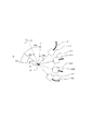
図1に示すように、本発明に係る露光装置1は、基台2、ステージ3、露光ユニット取付台4、マーキング露光用光源装置5、レーザ光切替器6、マーキング用露光ユニット7、周辺露光用光源装置8、周辺露光用露光ユニット9及び制御装置10を備える。露光装置1の上流側及び下流側には、ガラス基板Kを搬入及び搬出する手段としての移載ロボットやコンベアが配設される。露光装置1は、上流側から搬入されステージ3上に載置されたガラス基板Kにマーキング露光を行うと共に周辺露光を行い下流側に搬出する。なお、上流側とは図1における手前側であり、下流側とは同図における奥側である。
As shown in FIG. 1, the
基台2は、本露光装置1の各構成部を支える台座として機能し、その表面中央上にリニアモータ21がX方向に沿って設けられる。
The
ステージ3は、最も上流側の基板受取り位置と、最も下流側の基板送出し位置との間において、リニアモータ21の駆動により基台2上を等速度VでX方向に走行可能である。また、図示しない回転駆動機構により、垂直軸周りの回転動作も可能である。ステージ3の表面には、ガラス基板Kを吸着保持するための多数の吸着孔が穿設されると共に、ガラス基板Kの搬入及び搬出時に該ガラス基板Kを昇降させるためのリフトピンが出没可能に設けられる。なお、搬入されるガラス基板Kの表面にはフォトレジストが塗布されている。
The
露光ユニット取付台4は、ステージ3を跨ぐようにして設けられ、その上面にはマーキング露光用光源装置5、周辺露光用光源装置8及びレーザ光切替器6が取り付けられる。その上流側の端面には固定部材71を介してマーキング用露光ユニット7が合計3台取り付けられる。また、下流側の端面には周辺露光用露光ユニット9が合計3台取り付けられる。
The exposure unit mounting base 4 is provided so as to straddle the
マーキング露光用光源装置5は、通電によりレーザ光を生成するレーザダイオードを備え、光ファイバケーブル51によりレーザ光切替器6に接続される。周辺露光用光源装置8は、マーキング露光用光源装置5と同様に、通電によりレーザ光を生成するレーザダイオードを備え、光ファイバケーブル81により各周辺露光用露光ユニット9に接続される。
The marking exposure light source device 5 includes a laser diode that generates laser light when energized, and is connected to the
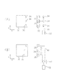
レーザ光切替器6は、図2に示すように、レンズ系61Aから61D、切替器用ガルバノミラー64及び切替器用ガルバノミラー駆動モータ65を備える。レンズ系61Dは、マーキング露光用光源装置5からのレーザ光を切替器用ガルバノミラー64に導くような配置とされる。切替器用ガルバノミラー64は、切替器用ガルバノミラー駆動モータ65により図中時計回り方向及び反時計回り方向に回動可能に軸支され、4つの角度位置θ0〜θ3に切り替えて配置可能とされる。角度位置θ0は基準となる待機位置である。レンズ系61Aから61Cは、各角度位置θ1からθ3に配置された切替器用ガルバノミラー64により偏向されるレーザ光をそれぞれ受光できるような配置とされる。
As shown in FIG. 2, the
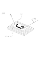
各マーキング用露光ユニット7Aから7Cは、光ファイバケーブル66A〜66Cによってレーザ光切替器6におけるそれぞれレンズ系61Aから61Cと接続される。そしてX方向及びY方向のそれぞれに沿って等間隔に配置される。その平面視は、図7に示すように、X方向について段違いに斜め列を呈する。互いに隣り合うマーキング用露光ユニット7A,7B及び7B,7Cは、露光終了位置P1から露光開始位置P2までが距離D1を有するように配置されている。また、各マーキング用露光ユニット7Aから7Cは、隣合う露光ユニット同士がぶつからない範囲でY方向にそれぞれ独立に移動可能に設けられる。これにより、Y方向についての露光位置に融通性をもたせることができる。
7C from each marking
各マーキング用露光ユニット7は、図3に示すように、反射ミラー71a、71b、ディジタルマイクロミラーデバイス(以下、単にDMDと記す)72、集光レンズ73、第1、第2露光ユニット用ガルバノミラー74、74Y、第1、第2露光ユニット用ガルバノミラー駆動モータ75、75Y、及びFθレンズ76を備え、DMD72により形成されるマーキング表示72Mをレーザ光によりガラス基板K上に導くように構成される。
As shown in FIG. 3, each marking exposure unit 7 includes reflection mirrors 71a and 71b, a digital micromirror device (hereinafter simply referred to as DMD) 72, a
DMDとは、図4,6に示すように、シリコンガラス基板上に格子状に多数(例えば1024×768個)配列されたそれぞれ14μm×14μmという微小なマイクロミラー721を、その反射角度を電気的に制御することによって画像を表示するように構成した素子である。オン状態では該マイクロミラー721への入射光が反射する角度とされ、オフ状態では反射しない角度とされる。例えばマーキングすべき文字が「G」である場合には、反射面が「G」字形を呈するようにマイクロミラー721の角度が変更される。前段落で述べたマーキング表示72Mは、このときに表示面に形成される画像のことである。
4 and 6, as shown in FIGS. 4 and 6, a
第1、第2露光ユニット用ガルバノミラー74、74Yは、図3に示すように、レーザ光の照射によるマーキング表示72Mのガラス基板Kへの像であるマーキング像MZがX方向に移動可能となるように駆動可能に設けられる。また、図5に示すように、第2露光ユニット用ガルバノミラー駆動モータ75Yにより第2露光ユニット用ガルバノミラー74Yを、マーキング像MZがY方向にも移動可能となるようにW2方向に駆動可能に設けることで、マーキング用露光ユニット7一台あたりのY方向についての露光範囲を広くすることができる。
As shown in FIG. 3, in the first and second exposure unit galvanometer mirrors 74 and 74Y , the marking image MZ, which is an image on the glass substrate K of the marking
制御装置10は、予め組み込まれたプログラムやオペレータによる入力操作に基づいて、図1に示す露光装置1に記載した各機器の動作制御を行う。
次に、図8から図10も参照して、以上のように構成された露光装置1の動作について説明する。図8及び図9はマーキング露光の動作を時系列的に説明するための平面概略図、図10は各露光ユニット7から出力されるレーザ光のオンオフ状態を示すタイムチャートである。なお、マーキング用露光ユニット7Aから7Cの各構成要素については、全て同一であるため、共通の符号で表記するが、説明上他と区別した方がわかりやすい場合は、例えば「74A」「74B」のように末尾に「A」から「C」のアルファベットを付して記述する。また、他のガルバノミラーや駆動モータについても同様な方法で記載する。
Next, the operation of the
図8(A)において、基板受取り位置に待機したステージ3は、上流側に配置されたロボットからガラス基板Kを受け取り、該ガラス基板Kをステージ3の表面上に吸着保持する。このとき、レーザ光切替器6における切替器用ガルバノミラー64は、待機位置である角度位置θ0にある。その後、ガラス基板Kを吸着保持した状態でステージ3はX1方向に等速度Vで走行すると共に、切替器用ガルバノミラー64は切替器用ガルバノミラー駆動モータ65により回動駆動されて角度位置θ0 から角度位置θ1となる。これにより、図2に示すように、レンズ系61Dを通過したマーキング露光用光源装置5からのレーザ光は、切替器用ガルバノミラー64の表面で反射してレンズ系61Aに向かう。そしてレンズ系61Aを通過した後、光ファイバケーブル66Aを介してマーキング用露光ユニット7Aに供給される。
In FIG. 8A, the
マーキング用露光ユニット7Aにおいて、レーザ光切替器6から供給され光ファイバーケーブル66Aを通じて送られてきたレーザ光は、図3に示すように、反射ミラー71aの反射面で反射した後、DMD72における表示面に照射される。該表示面では、ガラス基板Kにマーキングすべき所望の文字や記号に応じた反射形態を持たせるように、複数のマイクロミラー721がオンオフ制御されている。表示面で反射したレーザ光は、集光レンズ73で集光された後、第1、第2露光ユニット用ガルバノミラー74A、74YAに向かう。
In the marking
露光ユニット7Aの第1、第2露光ユニット用ガルバノミラー74A、74YAは、図10に示すように、レーザ光切替器6における切替器用ガルバノミラー64が角度位置θ1の位置となった後にオンとなる。オンとなった第1、第2露光ユニット用ガルバノミラー74A、74YAは、図5に示すように、第1露光ユニット用ガルバノミラー駆動モータ75によりt2秒間だけW1方向に等角速度で回動する。t2秒間という時間は、レーザ光を照射する時間であり、ステージ3がマーキング像MZのX方向距離D2を移動するのに要する時間に等しい。
First, second exposure unit for
第1、第2露光ユニット用ガルバノミラー74A、74YAにより進行方向が変化したレーザ光は、Fθレンズ76で収束された後、図8(B)に示すように、ガラス基板Kの表面に向けて照射される。そしてガラス基板Kの表面に塗布されたレジスト膜にDMD72で形成したマーキング表示72Mの露光が行われる。第1、第2露光ユニット用ガルバノミラー74A、74YAが図3に記載の様にW1方向に等角速度で回動することにより、ガラス基板K上に導かれるマーキング像MZはX1方向に等速度で移動する。ここで、第1、第2露光ユニット用ガルバノミラー74A、74YAは、マーキング像MZがX1方向に移動する速度と、ステージ3の走行速度Vとが等しくなるように回動する。これにより、露光ユニット7Aからガラス基板Kに照射されるレーザ光はステージ3と同期する。すなわち該レーザ光とステージ3との相対速度はゼロになる。このため、ステージ3とレーザ光との相対速度のずれから生じ得るマーキング像MZの伸びや滲みを防止することができる。
The laser light whose traveling direction is changed by the first and second exposure unit galvanometer mirrors 74A and 74YA is converged by the
なお、第1、第2露光ユニット用ガルバノミラー74A、74YAを駆動する代わりに、図6に示すように、DMD72に形成されるマーキング表示72Mを、ガラス基板K上に導かれるマーキング像MZがX1方向に等速度Vで移動するように、いわゆる「流し表示」することによっても同様な効果を得ることができる。「流し表示」とは、各マイクロミラー721のオンオフを所定方向に向けて等速度で順次シフトさせることにより、表示面上のマーキング表示72Mを、形を変えずに送り出して表示させることである。「流し表示」することにより、DMD72におけるマイクロミラー721が1枚程度破損していても、他のマイクロミラーがこれを補うので露光状態に支障を来さない。
Instead of driving the first and second exposure unit galvanometer mirrors 74A and 74YA , as shown in FIG. 6, the marking
図8(C)に示すように、露光ユニット7Aによるマーキング露光が終了すると、露光ユニット7Aの第1、第2露光ユニット用ガルバノミラー74A、74YAはオフとなり反転して元の角度位置に戻る。一方、レーザ光切替器6の切替器用ガルバノミラー64は、マーキング用露光ユニット7Aの第1、第2露光ユニット用ガルバノミラー74A、74YAがオフすると同時に切替器用ガルバノミラー駆動モータ65により角度位置θ1からW0方向に回動を開始して角度位置θ2となる。角度位置θ2となることにより、第1電源装置5から光ファイバケーブル51を介して供給されたレーザ光は、レンズ系61Dを通過した後、切替器用ガルバノミラー64の表面で反射してレンズ系61Bに向かう。そしてレンズ系61Bを通過した後、光ファイバケーブル66Bを介して露光ユニット7Bに供給される。
As shown in FIG. 8C, when the marking exposure by the
露光ユニット7Bの第1、第2露光ユニット用ガルバノミラー74B、74YBは、図10に示すように、マーキング用露光ユニット7Aの第1、第2露光ユニット用ガルバノミラー74A、74YAがオフとなってからt1秒後にオンとなり、第1露光ユニット用ガルバノミラー駆動モータ75BによりW1方向に等角速度で回動する。ここでt1秒という時間は、図7や図8(D)に示すように、マーキング用露光ユニット7Aの露光終了位置P1からマーキング用露光ユニット7Bの露光開始位置P2までの距離D1をステージ3が走行するのに要する時間である。つまりt1=D1/Vである。
As shown in FIG. 10, the first and second galvanometer mirrors 74A and 74YA of the marking
図9(E)に示すように、露光ユニット7Bによるマーキング露光が終了すると、露光ユニット7Bの第1、第2露光ユニット用ガルバノミラー74B、74YBはオフとなり反転して元の角度位置に戻る。一方、レーザ光切替器6の切替器用ガルバノミラー64は、マーキング用露光ユニット7Bの第1、第2露光ユニット用ガルバノミラー74B、74YBがオフすると同時に切替器用ガルバノミラー駆動モータ65により角度位置θ2からW0方向に回動を開始して角度位置θ3となる。角度位置θ3となることにより、第1電源装置5から光ファイバケーブル51を介して供給されたレーザ光は、レンズ系61Dを通過した後、切替器用ガルバノミラー64の表面で反射してレンズ系61Cに向かう。そしてレンズ系61Cを通過した後、光ファイバケーブル66Cを介してマーキング用露光ユニット7Cに供給される。マーキング用露光ユニット7Cの第1露光ユニット用ガルバノミラー74Cは、図10に示すように、マーキング用露光ユニット7Bの第1、第2露光ユニット用ガルバノミラー74B、74YBがオフとなってからt1秒後にオンとなり、第1、第2露光ユニット用ガルバノミラー駆動モータ75C、74YCによりW1方向に等角速度で回動する。
As shown in FIG. 9E , when the marking exposure by the
このように、露光装置1では、互いに隣り合う露光ユニット7A,7Bにおける一方の露光ユニット7Aの露光終了位置P1から他方の露光ユニット7Bの露光開始位置P2までの距離D1をステージ3が走行し終えたときに、他方の露光ユニット7Bからレーザ光を照射する。互いに隣り合う露光ユニット7は、露光終了位置P1から露光開始位置P2までが距離D1を有するような配置とされているため、一方の露光ユニット7Aによって形成されたマーキング像MZAと、他方の露光ユニット7Bによって形成されたマーキング像MZBとは、Y方向に一列となる。各露光ユニットから照射されるレーザ光は時系列的に切り替えられるので、レーザ光の照射数を増やした場合でも、光源の出力を大きなものにしたり、光源の数を増やしたりする必要がなく装置の低コスト化を図ることができる。
Thus, in the
また、DMD72を用いて面単位のマーキング表示72Mを露光しているので、従来のようにドット単位で露光する場合と異なり、露光位置にばらつきが生じることがなく、きれいなマーキング像MZを形成することができる。また、レーザ光とステージ3との相対速度がゼロになるため、ステージ3とレーザ光との相対速度のずれから生じ得るマーキング像MZの伸びや滲みを防止することができ、きれいなマーキング像MZを形成することができる。第1、第2露光ユニット用ガルバノミラー74、74Yは、マーキング像MZがY方向にも移動可能となるように駆動可能に設けられるので、マーキング用露光ユニット7一台あたりのY方向についての露光範囲を広くすることができる。
Further, since the marking
ステージ3のX1方向への走行に伴い、以上の動作を複数回繰り返すことにより、図9(H)に示すように、Y方向に一列となって並んだマーキング像MZA〜MZCを2次元的に形成することができる。
As the
更に露光装置1では、マーキング露光の動作と同時に周辺露光の動作も行う。周辺露光とは、パターン露光やマーキング露光とは別にガラス基板Kの周辺部を露光し、不要なレジストを除去する処理である。例えば、ガラス基板Kの周辺部全周を一定幅で周状に露光する全周露光や、ウエハ保持用の爪が接触する箇所のみを選択的に露光する部分露光がある。この処理の後に、現像工程を経て異物発生の原因となる不要レジストを除去する。
Further, the
露光装置1において、周辺露光は例えば次のように行う。すなわちマーキング露光の動作中において、ステージ3が上流側から下流側に向けて等速度Vで走行を開始すると共に、周辺露光用露光ユニット9A,9Cがオンとなり、周辺露光用光源装置8から供給されたレーザ光がガラス基板KにおけるY方向についての両端部に向けて照射される。ステージ3がX1方向に走行することにより、ガラス基板KにおけるX方向に平行な両周辺部に露光が行われる。このように、マーキング露光と同時に周辺露光を行うので、タクト時間の短縮化を図ることができる。
In the
なお、該ガラス基板Kにおける残りの両周辺部にも露光を行いたい場合は、ステージ3を回転駆動機構により下流側で垂直軸周りに90度回転させた後、走行方向を反転させてX2方向に等速度(−V)で走行させる。これにより、残りの両周辺部にも露光が行われる。
If exposure is to be performed on both remaining peripheral portions of the glass substrate K, the
また、該ガラス基板Kの中央線付近も一直線状に露光したい場合は、中央の露光ユニット9Bからもレーザ光を照射して上と同様にして露光する。
When it is desired to expose the vicinity of the center line of the glass substrate K in a straight line, the exposure is performed in the same manner as above by irradiating laser light from the
以上、本発明の実施の形態について説明を行ったが、上に開示した実施の形態は、あくまで例示であって、本発明の範囲はこれら実施の形態に限定されるものではない。本発明の範囲は、特許請求の範囲の記載によって示され、更に特許請求の範囲と均等の意味及び範囲内でのすべての変更を含むことが意図される。 As mentioned above, although embodiment of this invention was described, embodiment disclosed above is an illustration to the last, Comprising: The scope of the present invention is not limited to these embodiment. The scope of the present invention is defined by the terms of the claims, and is intended to include any modifications within the scope and meaning equivalent to the terms of the claims.
例えば、請求項における「複数のマーキング用露光ユニット」は、上に開示した実施の形態では、各マーキング用露光ユニットが一つ一つ独立したケーシングであり、その中に種々の光学的機構要素を収納したものとしたが、必ずしもケーシングが一つ一つ独立していなくてもよい。すなわちケーシングが独立していなくても同様の機能を備える構成、例えば、上と同様な種々の光学的機構要素を一つのケーシング内に複数段収納している構成であっても、本発明の範囲内であると解釈する。 For example, "a plurality of marking the exposure unit" in the claims, in the embodiment disclosed above, is to case sheet ring in which each marking EXPOSURE units one by one separate, various optical therein However, the casings do not necessarily have to be independent one by one. That is, even if the casing has a structure having the same function even if it is not independent, for example, a structure in which various optical mechanism elements similar to the above are housed in a plurality of stages in one casing, the scope of the present invention. To be interpreted as
また、上に開示した実施の形態では、マーキング用露光ユニット7及び周辺露光用露光ユニット9をそれぞれ3台の配置として示したが、2台または4台以上の配置としてもよい。また、これらのマーキング用露光ユニット7,9を固定したままでステージ3を走行させる形態を示したが、ステージ3を固定しておきマーキング用露光ユニット7,9を走行させる形態、またはステージ3とマーキング用露光ユニット7,9の両方を走行させる形態としてもよい。
[図面の簡単な説明]
Further, in the embodiment disclosed above, it showed marking EXPOSURE unit 7 and the peripheral
[Brief description of drawings]
[符号の説明]
1 露光装置
3 ステージ
5 マーキング露光用光源装置
7 マーキング用露光ユニット
8.周辺露光用光源装置
9 周辺露光用露光ユニット
64 切替器用ガルバノミラー
65 切替器用ガルバノミラー駆動モータ
72 ディジタルマイクロミラーデバイス(DMD)
72M マーキング表示
74 第1露光ユニット用ガルバノミラー
74Y 第2露光ユニット用ガルバノミラー
75 第1露光ユニット用ガルバノミラー駆動モータ
75Y 第2露光ユニット用ガルバノミラー駆動モータ
D1 距離
K ガラス基板(被露光基板)
MZ マーキング像
P1 露光終了位置
P2 露光開始位置
X 方向(相対移動の方向)
Y 方向(相対移動の方向と直交する方向)
[Explanation of symbols]
1
8). EXPOSURE unit
64 switching
MZ marking image P1 exposure end position P2 exposure start position X direction (direction of relative movement)
Y direction (direction perpendicular to the direction of relative movement)
Claims (2)
被露光基板を載置するためのステージと、
前記ステージに対して等速度で相対移動可能に設けられると共に前記ステージの上部に平面視が前記相対移動の方向について段違いに斜め列となるように配置されそれぞれディジタルマイクロミラーデバイスにより形成されるマーキング表示を前記レーザ光により前記被露光基板上に照射するように構成された複数のマーキング用露光ユニットと、
互いに隣り合うマーキング用露光ユニットにおける一方のマーキング用露光ユニットの露光終了位置から他方のマーキング用露光ユニットの露光開始位置までの距離を前記ステージと前記複数のマーキング用露光ユニットとが相対移動する毎に、前記被露光基板上を最初に通過するマーキング用露光ユニットから前記被露光基板上を最後に通過するマーキング用露光ユニットへ向かう順序で、各マーキング用露光ユニットが前記被露光基板上に照射するレーザ光を切り替える切替手段と
を備え、
前記複数のマーキング用露光ユニットを前記ステージに対して相対移動させながら、前記切替手段によるレーザー光の切り替え、および、各マーキング用露光ユニットによるレーザ光の照射を行うことを特徴とする露光装置。 A light source device for marking exposure that generates laser light for marking exposure;
A stage for mounting the substrate to be exposed;
Marking display provided by the digital micromirror device, which is provided so as to be relatively movable with respect to the stage at a constant speed, and is arranged in an oblique row in a plan view on the upper part of the stage with respect to the direction of the relative movement. A plurality of marking exposure units configured to irradiate the exposed substrate with the laser beam,
Every time the stage and the plurality of marking exposure units move relative to each other, the distance from the exposure end position of one marking exposure unit to the exposure start position of the other marking exposure unit in the adjacent marking exposure units the order directed from marking the exposure unit to first pass through the exposed upper substrate to marking the exposure unit passing through the object to be exposed on the substrate Finally, lasers each marking exposure unit for irradiating the object to be exposed on the substrate Switching means for switching light , and
An exposure apparatus that performs switching of laser light by the switching means and irradiation of laser light by each marking exposure unit while moving the plurality of marking exposure units relative to the stage .
ステージ上に被露光基板を載置し、
複数のマーキング用露光ユニットを前記ステージに対して等速度で相対移動可能に設けると共に
前記ステージの上部に平面視が前記相対移動の方向について段違いに斜め列となるように配置し、
それぞれのマーキング用露光ユニットにおけるディジタルマイクロミラーデバイスにより形成されるマーキング表示を、互いに隣り合うマーキング用露光ユニットにおける一方のマーキング用露光ユニットの露光終了位置から他方のマーキング用露光ユニットの露光開始位置までの距離を前記ステージと前記複数のマーキング用露光ユニットとが相対移動する毎に、前記被露光基板上を最初に通過するマーキング用露光ユニットから前記被露光基板上を最後に通過するマーキング用露光ユニットへ向かう順序で、各マーキング用露光ユニットが前記被露光基板上に照射するレーザ光を切り替えることにより、前記被露光基板上に導き、
前記複数のマーキング用露光ユニットを前記ステージに対して相対移動させながら、レーザー光の切り替え、および、各マーキング用露光ユニットによるレーザ光の照射を行うことを特徴とする露光方法。 The marking exposure light source device generates laser light for marking exposure,
Place the substrate to be exposed on the stage,
A plurality of marking exposure units are provided so as to be relatively movable with respect to the stage at a constant speed, and are arranged on the upper part of the stage so that the plan view is inclined in a row with respect to the direction of the relative movement,
The marking display formed by the digital micromirror device in each marking exposure unit is displayed from the exposure end position of one marking exposure unit to the exposure start position of the other marking exposure unit in the adjacent marking exposure units. Each time the stage and the plurality of marking exposure units move relative to each other, the marking exposure unit that first passes over the exposed substrate changes to the marking exposure unit that passes last over the exposed substrate. By switching the laser light irradiated on the substrate to be exposed by each marking exposure unit in the order to go, it is guided onto the substrate to be exposed ,
An exposure method comprising: switching a laser beam and irradiating each marking exposure unit with a laser beam while moving the plurality of marking exposure units relative to the stage .
Priority Applications (4)
| Application Number | Priority Date | Filing Date | Title |
|---|---|---|---|
| JP2005079425A JP4664102B2 (en) | 2005-03-18 | 2005-03-18 | Exposure apparatus and exposure method |
| TW095107019A TW200643648A (en) | 2005-03-18 | 2006-03-02 | Exposure apparatus and exposure method |
| KR1020060024663A KR100908548B1 (en) | 2005-03-18 | 2006-03-17 | Exposure apparatus and exposure method |
| CNB2006100655013A CN100517076C (en) | 2005-03-18 | 2006-03-20 | Exposal device and method |
Applications Claiming Priority (1)
| Application Number | Priority Date | Filing Date | Title |
|---|---|---|---|
| JP2005079425A JP4664102B2 (en) | 2005-03-18 | 2005-03-18 | Exposure apparatus and exposure method |
Related Child Applications (1)
| Application Number | Title | Priority Date | Filing Date |
|---|---|---|---|
| JP2010259030A Division JP2011034123A (en) | 2010-11-19 | 2010-11-19 | Exposure apparatus and exposure method |
Publications (3)
| Publication Number | Publication Date |
|---|---|
| JP2006259515A JP2006259515A (en) | 2006-09-28 |
| JP2006259515A5 JP2006259515A5 (en) | 2007-07-26 |
| JP4664102B2 true JP4664102B2 (en) | 2011-04-06 |
Family
ID=37002592
Family Applications (1)
| Application Number | Title | Priority Date | Filing Date |
|---|---|---|---|
| JP2005079425A Active JP4664102B2 (en) | 2005-03-18 | 2005-03-18 | Exposure apparatus and exposure method |
Country Status (4)
| Country | Link |
|---|---|
| JP (1) | JP4664102B2 (en) |
| KR (1) | KR100908548B1 (en) |
| CN (1) | CN100517076C (en) |
| TW (1) | TW200643648A (en) |
Families Citing this family (11)
| Publication number | Priority date | Publication date | Assignee | Title |
|---|---|---|---|---|
| JP4491446B2 (en) * | 2005-11-04 | 2010-06-30 | 株式会社オーク製作所 | Peripheral exposure apparatus and method |
| JP4491447B2 (en) * | 2005-11-04 | 2010-06-30 | 株式会社オーク製作所 | Laser beam / ultraviolet irradiation peripheral exposure apparatus and method |
| JP4491444B2 (en) * | 2005-11-04 | 2010-06-30 | 株式会社オーク製作所 | Laser beam / ultraviolet irradiation peripheral exposure apparatus and method |
| JP4491445B2 (en) * | 2005-11-04 | 2010-06-30 | 株式会社オーク製作所 | Peripheral exposure apparatus and method |
| JP4533874B2 (en) * | 2005-11-04 | 2010-09-01 | 株式会社オーク製作所 | Laser beam exposure system |
| CN100593469C (en) * | 2007-02-12 | 2010-03-10 | 深圳市大族激光科技股份有限公司 | Modularization exposure system |
| JP2011013512A (en) * | 2009-07-03 | 2011-01-20 | Orc Manufacturing Co Ltd | Peripheral exposure apparatus |
| TWI454687B (en) * | 2009-08-03 | 2014-10-01 | Toray Eng Co Ltd | Marking device and method |
| CN102514385B (en) * | 2011-11-29 | 2015-04-15 | 深圳市华星光电技术有限公司 | Identification code printing method and identification code printing device |
| JP5896459B2 (en) | 2012-03-06 | 2016-03-30 | 東レエンジニアリング株式会社 | Marking apparatus and method |
| CN109116593B (en) * | 2018-08-02 | 2021-07-20 | 深圳市华星光电半导体显示技术有限公司 | Method for exposing master plate |
Citations (7)
| Publication number | Priority date | Publication date | Assignee | Title |
|---|---|---|---|---|
| JPH08150485A (en) * | 1994-11-28 | 1996-06-11 | Komatsu Ltd | Laser marking device |
| JPH08224675A (en) * | 1995-02-22 | 1996-09-03 | Toshiba Corp | Device for forming marking pattern |
| JP2001174721A (en) * | 1999-12-20 | 2001-06-29 | Yaskawa Electric Corp | Plotter |
| JP2001205462A (en) * | 2000-01-26 | 2001-07-31 | Nec Corp | Laser marking device and method of laser marking |
| JP2002091012A (en) * | 2000-09-20 | 2002-03-27 | Toray Eng Co Ltd | Aligner |
| JP2003131392A (en) * | 2001-10-25 | 2003-05-09 | Mitsubishi Corp | Marking method and apparatus by laser beam |
| JP2003290939A (en) * | 2002-03-28 | 2003-10-14 | Sunx Ltd | Laser marking device |
Family Cites Families (1)
| Publication number | Priority date | Publication date | Assignee | Title |
|---|---|---|---|---|
| KR100322621B1 (en) * | 1999-12-31 | 2002-03-18 | 황인길 | Device for marking identification using the athletic liquid crystal display |
-
2005
- 2005-03-18 JP JP2005079425A patent/JP4664102B2/en active Active
-
2006
- 2006-03-02 TW TW095107019A patent/TW200643648A/en unknown
- 2006-03-17 KR KR1020060024663A patent/KR100908548B1/en active IP Right Grant
- 2006-03-20 CN CNB2006100655013A patent/CN100517076C/en active Active
Patent Citations (7)
| Publication number | Priority date | Publication date | Assignee | Title |
|---|---|---|---|---|
| JPH08150485A (en) * | 1994-11-28 | 1996-06-11 | Komatsu Ltd | Laser marking device |
| JPH08224675A (en) * | 1995-02-22 | 1996-09-03 | Toshiba Corp | Device for forming marking pattern |
| JP2001174721A (en) * | 1999-12-20 | 2001-06-29 | Yaskawa Electric Corp | Plotter |
| JP2001205462A (en) * | 2000-01-26 | 2001-07-31 | Nec Corp | Laser marking device and method of laser marking |
| JP2002091012A (en) * | 2000-09-20 | 2002-03-27 | Toray Eng Co Ltd | Aligner |
| JP2003131392A (en) * | 2001-10-25 | 2003-05-09 | Mitsubishi Corp | Marking method and apparatus by laser beam |
| JP2003290939A (en) * | 2002-03-28 | 2003-10-14 | Sunx Ltd | Laser marking device |
Also Published As
| Publication number | Publication date |
|---|---|
| TWI350946B (en) | 2011-10-21 |
| KR100908548B1 (en) | 2009-07-20 |
| KR20060101337A (en) | 2006-09-22 |
| CN1834789A (en) | 2006-09-20 |
| JP2006259515A (en) | 2006-09-28 |
| CN100517076C (en) | 2009-07-22 |
| TW200643648A (en) | 2006-12-16 |
Similar Documents
| Publication | Publication Date | Title |
|---|---|---|
| JP4664102B2 (en) | Exposure apparatus and exposure method | |
| TW594433B (en) | Pattern writing apparatus and pattern writing method | |
| JPH113849A (en) | Deformable illumination filter and semiconductor aligner | |
| JP2009537324A (en) | Method and tool for patterning a thin film on a moving substrate | |
| KR100816494B1 (en) | A maskless exposure apparatus and a manufacturing method for display substrate using thereof | |
| JP2011034123A (en) | Exposure apparatus and exposure method | |
| JP4235972B2 (en) | Pattern drawing apparatus and pattern drawing method | |
| JP4356161B2 (en) | Drawing device | |
| KR20080109608A (en) | Drawing system, drawing apparatus and drawing method | |
| US20110205508A1 (en) | Digital Exposure Method and Digital Exposure Device for Performing the Method | |
| KR100995392B1 (en) | Marking apparatus having digital micromirror device | |
| JP5219982B2 (en) | Exposure apparatus, exposure method, and manufacturing method of display panel substrate | |
| JP4169264B2 (en) | Light beam generator | |
| JP5360379B2 (en) | Projection optical system, exposure apparatus, and device manufacturing method | |
| KR100799500B1 (en) | Dry eaching device with polygonal scanner and galvanometer scanner | |
| WO2007071408A1 (en) | Slm direct writer | |
| JP2008046457A (en) | Drawing device | |
| KR20070078243A (en) | An exposing apparatus for marking using a micro mirror array | |
| KR100904039B1 (en) | Multi-head laser direct imaging system | |
| JP5253037B2 (en) | Exposure apparatus, exposure method, and manufacturing method of display panel substrate | |
| JP2005243870A (en) | Pattern drawing apparatus | |
| JP2004054101A (en) | Laser direct plotting device having automatic resolution setting function | |
| KR100958574B1 (en) | Apparatus and method fabrication liquid crystal display device | |
| WO2006049330A1 (en) | Exposure equipment | |
| JP4713223B2 (en) | Pattern transfer apparatus and transfer method |
Legal Events
| Date | Code | Title | Description |
|---|---|---|---|
| A521 | Request for written amendment filed |
Free format text: JAPANESE INTERMEDIATE CODE: A523 Effective date: 20070613 |
|
| A621 | Written request for application examination |
Free format text: JAPANESE INTERMEDIATE CODE: A621 Effective date: 20070613 |
|
| A977 | Report on retrieval |
Free format text: JAPANESE INTERMEDIATE CODE: A971007 Effective date: 20100210 |
|
| A131 | Notification of reasons for refusal |
Free format text: JAPANESE INTERMEDIATE CODE: A131 Effective date: 20100511 |
|
| A521 | Request for written amendment filed |
Free format text: JAPANESE INTERMEDIATE CODE: A523 Effective date: 20100709 |
|
| A521 | Request for written amendment filed |
Free format text: JAPANESE INTERMEDIATE CODE: A523 Effective date: 20100716 |
|
| A02 | Decision of refusal |
Free format text: JAPANESE INTERMEDIATE CODE: A02 Effective date: 20100823 |
|
| A521 | Request for written amendment filed |
Free format text: JAPANESE INTERMEDIATE CODE: A523 Effective date: 20101119 |
|
| A911 | Transfer to examiner for re-examination before appeal (zenchi) |
Free format text: JAPANESE INTERMEDIATE CODE: A911 Effective date: 20101129 |
|
| TRDD | Decision of grant or rejection written | ||
| A01 | Written decision to grant a patent or to grant a registration (utility model) |
Free format text: JAPANESE INTERMEDIATE CODE: A01 Effective date: 20101228 |
|
| A01 | Written decision to grant a patent or to grant a registration (utility model) |
Free format text: JAPANESE INTERMEDIATE CODE: A01 |
|
| A61 | First payment of annual fees (during grant procedure) |
Free format text: JAPANESE INTERMEDIATE CODE: A61 Effective date: 20110106 |
|
| R150 | Certificate of patent or registration of utility model |
Ref document number: 4664102 Country of ref document: JP Free format text: JAPANESE INTERMEDIATE CODE: R150 |
|
| FPAY | Renewal fee payment (event date is renewal date of database) |
Free format text: PAYMENT UNTIL: 20140114 Year of fee payment: 3 |
|
| R250 | Receipt of annual fees |
Free format text: JAPANESE INTERMEDIATE CODE: R250 |
|
| R250 | Receipt of annual fees |
Free format text: JAPANESE INTERMEDIATE CODE: R250 |
|
| R250 | Receipt of annual fees |
Free format text: JAPANESE INTERMEDIATE CODE: R250 |
|
| R250 | Receipt of annual fees |
Free format text: JAPANESE INTERMEDIATE CODE: R250 |
|
| R250 | Receipt of annual fees |
Free format text: JAPANESE INTERMEDIATE CODE: R250 |
|
| R250 | Receipt of annual fees |
Free format text: JAPANESE INTERMEDIATE CODE: R250 |
|
| R250 | Receipt of annual fees |
Free format text: JAPANESE INTERMEDIATE CODE: R250 |
|
| R250 | Receipt of annual fees |
Free format text: JAPANESE INTERMEDIATE CODE: R250 |
|
| R250 | Receipt of annual fees |
Free format text: JAPANESE INTERMEDIATE CODE: R250 |
|
| R250 | Receipt of annual fees |
Free format text: JAPANESE INTERMEDIATE CODE: R250 |
|
| R250 | Receipt of annual fees |
Free format text: JAPANESE INTERMEDIATE CODE: R250 |