JP4659751B2 - Method for forming a low-K dielectric in a semiconductor manufacturing process - Google Patents
Method for forming a low-K dielectric in a semiconductor manufacturing process Download PDFInfo
- Publication number
- JP4659751B2 JP4659751B2 JP2006536603A JP2006536603A JP4659751B2 JP 4659751 B2 JP4659751 B2 JP 4659751B2 JP 2006536603 A JP2006536603 A JP 2006536603A JP 2006536603 A JP2006536603 A JP 2006536603A JP 4659751 B2 JP4659751 B2 JP 4659751B2
- Authority
- JP
- Japan
- Prior art keywords
- dielectric layer
- layer
- forming
- low
- dielectric
- Prior art date
- Legal status (The legal status is an assumption and is not a legal conclusion. Google has not performed a legal analysis and makes no representation as to the accuracy of the status listed.)
- Expired - Fee Related
Links
Images
Classifications
-
- H—ELECTRICITY
- H01—ELECTRIC ELEMENTS
- H01L—SEMICONDUCTOR DEVICES NOT COVERED BY CLASS H10
- H01L21/00—Processes or apparatus adapted for the manufacture or treatment of semiconductor or solid state devices or of parts thereof
- H01L21/02—Manufacture or treatment of semiconductor devices or of parts thereof
- H01L21/04—Manufacture or treatment of semiconductor devices or of parts thereof the devices having at least one potential-jump barrier or surface barrier, e.g. PN junction, depletion layer or carrier concentration layer
- H01L21/18—Manufacture or treatment of semiconductor devices or of parts thereof the devices having at least one potential-jump barrier or surface barrier, e.g. PN junction, depletion layer or carrier concentration layer the devices having semiconductor bodies comprising elements of Group IV of the Periodic System or AIIIBV compounds with or without impurities, e.g. doping materials
- H01L21/30—Treatment of semiconductor bodies using processes or apparatus not provided for in groups H01L21/20 - H01L21/26
- H01L21/302—Treatment of semiconductor bodies using processes or apparatus not provided for in groups H01L21/20 - H01L21/26 to change their surface-physical characteristics or shape, e.g. etching, polishing, cutting
-
- H—ELECTRICITY
- H01—ELECTRIC ELEMENTS
- H01L—SEMICONDUCTOR DEVICES NOT COVERED BY CLASS H10
- H01L21/00—Processes or apparatus adapted for the manufacture or treatment of semiconductor or solid state devices or of parts thereof
- H01L21/02—Manufacture or treatment of semiconductor devices or of parts thereof
- H01L21/02041—Cleaning
- H01L21/02057—Cleaning during device manufacture
- H01L21/0206—Cleaning during device manufacture during, before or after processing of insulating layers
- H01L21/02063—Cleaning during device manufacture during, before or after processing of insulating layers the processing being the formation of vias or contact holes
-
- H—ELECTRICITY
- H01—ELECTRIC ELEMENTS
- H01L—SEMICONDUCTOR DEVICES NOT COVERED BY CLASS H10
- H01L21/00—Processes or apparatus adapted for the manufacture or treatment of semiconductor or solid state devices or of parts thereof
- H01L21/70—Manufacture or treatment of devices consisting of a plurality of solid state components formed in or on a common substrate or of parts thereof; Manufacture of integrated circuit devices or of parts thereof
- H01L21/71—Manufacture of specific parts of devices defined in group H01L21/70
- H01L21/768—Applying interconnections to be used for carrying current between separate components within a device comprising conductors and dielectrics
- H01L21/76801—Applying interconnections to be used for carrying current between separate components within a device comprising conductors and dielectrics characterised by the formation and the after-treatment of the dielectrics, e.g. smoothing
- H01L21/76822—Modification of the material of dielectric layers, e.g. grading, after-treatment to improve the stability of the layers, to increase their density etc.
- H01L21/76826—Modification of the material of dielectric layers, e.g. grading, after-treatment to improve the stability of the layers, to increase their density etc. by contacting the layer with gases, liquids or plasmas
-
- H—ELECTRICITY
- H01—ELECTRIC ELEMENTS
- H01L—SEMICONDUCTOR DEVICES NOT COVERED BY CLASS H10
- H01L21/00—Processes or apparatus adapted for the manufacture or treatment of semiconductor or solid state devices or of parts thereof
- H01L21/70—Manufacture or treatment of devices consisting of a plurality of solid state components formed in or on a common substrate or of parts thereof; Manufacture of integrated circuit devices or of parts thereof
- H01L21/71—Manufacture of specific parts of devices defined in group H01L21/70
- H01L21/768—Applying interconnections to be used for carrying current between separate components within a device comprising conductors and dielectrics
- H01L21/76801—Applying interconnections to be used for carrying current between separate components within a device comprising conductors and dielectrics characterised by the formation and the after-treatment of the dielectrics, e.g. smoothing
- H01L21/76829—Applying interconnections to be used for carrying current between separate components within a device comprising conductors and dielectrics characterised by the formation and the after-treatment of the dielectrics, e.g. smoothing characterised by the formation of thin functional dielectric layers, e.g. dielectric etch-stop, barrier, capping or liner layers
- H01L21/76832—Multiple layers
-
- H—ELECTRICITY
- H01—ELECTRIC ELEMENTS
- H01L—SEMICONDUCTOR DEVICES NOT COVERED BY CLASS H10
- H01L21/00—Processes or apparatus adapted for the manufacture or treatment of semiconductor or solid state devices or of parts thereof
- H01L21/70—Manufacture or treatment of devices consisting of a plurality of solid state components formed in or on a common substrate or of parts thereof; Manufacture of integrated circuit devices or of parts thereof
- H01L21/71—Manufacture of specific parts of devices defined in group H01L21/70
- H01L21/768—Applying interconnections to be used for carrying current between separate components within a device comprising conductors and dielectrics
- H01L21/76801—Applying interconnections to be used for carrying current between separate components within a device comprising conductors and dielectrics characterised by the formation and the after-treatment of the dielectrics, e.g. smoothing
- H01L21/76829—Applying interconnections to be used for carrying current between separate components within a device comprising conductors and dielectrics characterised by the formation and the after-treatment of the dielectrics, e.g. smoothing characterised by the formation of thin functional dielectric layers, e.g. dielectric etch-stop, barrier, capping or liner layers
- H01L21/76834—Applying interconnections to be used for carrying current between separate components within a device comprising conductors and dielectrics characterised by the formation and the after-treatment of the dielectrics, e.g. smoothing characterised by the formation of thin functional dielectric layers, e.g. dielectric etch-stop, barrier, capping or liner layers formation of thin insulating films on the sidewalls or on top of conductors
-
- H—ELECTRICITY
- H01—ELECTRIC ELEMENTS
- H01L—SEMICONDUCTOR DEVICES NOT COVERED BY CLASS H10
- H01L21/00—Processes or apparatus adapted for the manufacture or treatment of semiconductor or solid state devices or of parts thereof
- H01L21/02—Manufacture or treatment of semiconductor devices or of parts thereof
- H01L21/02041—Cleaning
- H01L21/02043—Cleaning before device manufacture, i.e. Begin-Of-Line process
- H01L21/02054—Cleaning before device manufacture, i.e. Begin-Of-Line process combining dry and wet cleaning steps
Description
本発明は集積回路製造に関し、特に低K誘電体膜を集積回路製造において形成する方法に関する。 The present invention relates to integrated circuit manufacturing, and more particularly to a method of forming a low-K dielectric film in integrated circuit manufacturing.
半導体の製造では、開発対象の一つは、低K誘電体を層間誘電体(interlayer dielectric:ILD)、すなわち半導体基板上の複数の導電層の間の層に使用することである。この低K誘電体は、配線として使用する複数の導体の間の容量結合を小さくするように作用する。この容量結合を小さくすることは、多くの場合がそうであるように、速度に高い優先度が置かれる場合において特に重要となる。低K材料は通常、最良の絶縁体でもなく、最も製造し易く高歩留まりをもたらす訳でもない。多くの場合、バリア層及びキャップ層は、正しい動作を行なうために必要な特性の全てを実現するために必要とされる。これらの追加の層によって追加の工程が生じ、これらの工程によってプロセスが複雑になり、かつ歩留まり低下の問題が生じ得る。 In semiconductor manufacturing, one of the development targets is to use low-K dielectrics for interlevel dielectrics (ILDs), that is, layers between multiple conductive layers on a semiconductor substrate. This low-K dielectric acts to reduce capacitive coupling between a plurality of conductors used as wiring. Reducing this capacitive coupling is particularly important when speed is a high priority, as is often the case. Low-K materials are usually not the best insulators and are not the easiest to manufacture and do not yield high yields. In many cases, the barrier layer and cap layer are required to achieve all of the properties necessary for proper operation. These additional layers create additional steps, which can complicate the process and cause yield degradation problems.
従って、歩留まりへの悪影響を小さくしながら形成することができる低K誘電体が半導体製造において必要になる。 Therefore, a low K dielectric that can be formed while reducing the negative impact on yield is required in semiconductor manufacturing.
本発明は例を通して示され、そして添付の図によって制限されるものではなく、これらの図では、同様の参照記号は同様の構成要素を指す。
当業者であれば、これらの図における構成要素が説明を簡単かつ明瞭にするために示され、そして必ずしも寸法通りには描かれていないことが分かるであろう。例えば、これらの図における幾つかの構成要素の寸法を他の構成要素に対して誇張して描いて本発明の実施形態を理解し易くしている。
The present invention is illustrated through examples and is not limited by the accompanying figures, in which like reference numerals refer to like components.
Those skilled in the art will appreciate that the components in these figures are shown for simplicity and clarity of illustration and are not necessarily drawn to scale. For example, the dimensions of some components in these figures are exaggerated relative to other components to facilitate understanding of embodiments of the present invention.
一の形態では、疎水性表面を有するように堆積させる低kバリア層は、酸素プラズマで処理して表面を親水性に改質する。次に親水性表面に対して、スクラブによる洗浄を行なう。スクラブによる効果は表面が親水性であることに起因して著しく増大する。処理の後、低K誘電体層を表面の上に形成する。この様子は、図及び次の記述を参照することにより更に深く理解される。 In one form, the low-k barrier layer deposited to have a hydrophobic surface is treated with oxygen plasma to modify the surface to be hydrophilic. Next, scrubbing is performed on the hydrophilic surface. The effect of scrub is greatly increased due to the hydrophilic surface. After processing, a low K dielectric layer is formed on the surface. This can be better understood with reference to the figures and the following description.
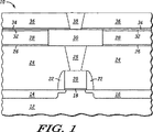
図1に示すのは半導体素子10であり、この半導体素子は半導体基板12と、基板12に形成されるドレイン領域14と、基板12に形成されるソース領域16と、基板12上に位置し、かつドレイン14とソース16との間にほぼ位置するゲート誘電体18と、ゲート誘電体18上のゲート20と、ゲート20周辺のサイドウォールスペーサ22と、ゲート20の上及び周辺の誘電体層24と、ゲート20上のコンタクト25と、誘電体層24上の低kバリア誘電体層26と、低kバリア誘電体層26上の低K誘電体層28と、低K誘電体層28上のキャップ層32と、ビア25上に位置し、かつ層26,28,及び30によって取り囲まれる導電層30と、キャップ層32上の低kバリア層34と、低kバリア層34上の低K誘電体層36と、そして導電層30上に位置し、かつ層34及び36によって取り囲まれるビア38と、を備える。半導体基板12はSOI基板であることが好ましく、SOI基板では、半導体はシリコンである、または半導体は、別の半導体材料から成る別のタイプの半導体基板とすることができる。ゲート20はシリコンであることが好ましいが、金属のような他の材料、または異なる層から成る複合層とすることができる。コンタクト25はタングステンであることが好ましいが、別のタイプの導電材料とすることができる。ビア38は銅であることが好ましいが、別のタイプの導電材料とするこ
とができる。導電層30は銅であることが好ましいが、別の導電材料とすることができる。キャップ層32は、テトラエチルオルトシリケート(TEOS)を使用して形成される酸化物であることが好ましいが、他の誘電体材料とすることができる。誘電体24は複合層であり、上層はSiCOH、またはフッ素及びTEOS(FTEOS)を使用して形成される酸化物のいずれかであることが好ましい。CMPプロセスを誘電体層24に適用して、CMP処理後の層24の表面上の材料を変えることができるようにする。CMPプロセスを実行する前の層24上の材料の好適な組み合わせは、シリコンリッチな酸化物、シリコンリッチな酸窒化物、TEOS酸化物であり、この組み合わせにより、層24の上部表面は、素子10が形成されるウェハ全体に渡って同じとはならない。半導体素子10は、低kバリア層26及び低K誘電体28から成る複合層、及び低kバリア層34及び低K誘電体層36から成る複合層を形成する方法を除いた従来の手段によって形成することができる従来構造である。
FIG. 1 shows a semiconductor element 10, which is located on a
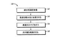
これらの複合層を形成する方法は図2のフロー図50に示される。フロー図50は、工程52,54,56,及び58を含む。工程52では、疎水性表面を有する層を堆積させ、この層は低Kバリア層26及び34に該当する。バリア層26及び34はSiCNであることが好ましい。低K誘電体層28及び36はSiCOHであることが好ましい。SiCNは、SiCOHを層24から保護するための有効なバリアであることが判明している。SiCNは疎水性表面を有する特徴を備える。SiCNはまた、その表面上にパーティクルを有することが判明している。スクラブ洗浄では、パーティクルの全てを除去するということはできないことが判っている。この洗浄が完全に有効となるまでには至らないことについて考えられる理由の一つに、SiCN層の表面が堆積直後の状態において、疎水性になっていることが考えられる。更に、スクラブ洗浄はSiCN構造にダメージを与えて新規のタイプの欠陥を生成することが判明している。ステップ54では、SiCN層の表面を疎水性から親水性に改質させる。これは、酸素プラズマを使用して行なわれる。SiCNの堆積及びSiCN層に対する後続のプラズマ処理はin−situ(その場)で行なうことが好ましい。SiCNはプラズマを用いて堆積させるので、後続の酸素プラズマ工程は、ウェハを堆積チャンバーから取り外す必要を生じることなく容易に行なうことができる。従って、層26を堆積させ、次に同じチャンバーで処理する。導体30を堆積させ、そしてCMP処理した後であるが、同じ方法で、層34も堆積させ、次に同じチャンバーで処理する。
The method of forming these composite layers is shown in the flow diagram 50 of FIG. Flow diagram 50 includes
工程56では、プラズマ処理を施した層の表面のスクラブを行なう。従って、層26は、層26を酸素プラズマ処理した後に、スクラブ洗浄処理する。この処理は層34に対しても行なわれる。スクラブ洗浄は水を用いた洗浄である。水は脱イオン化することが好ましく、更に水酸化アンモニウムを含む。これは、スクラブ洗浄のような水を用いた洗浄に関する従来の組成である。
In
工程58では、次の層の堆積を行なうが、次の層は、低kバリア層26上の低K誘電体層28及びバリア層34上の低K誘電体層36である。工程52〜58をこのように組み合わせることにより、低K誘電体層として有用な複合層が完成する。
この方法が利点をもたらす理由の一つは、バリア層をプラズマ堆積することにより、歩留まりを低下させる欠陥を生じさせ得るバリア表面上のパーティクルが減るからである。これらのパーティクルは、スクラブによっては効果的に取り除くことができない、というのは、バリア層の表面が疎水性であるからである。更に、バリア層表面に対するバリア層堆積後のプラズマ処理によって、バリア層表面が親水性に改質されるので、スクラブは、新規の欠陥タイプを後の工程において発生させることなくパーティクルを取り除くために有効となる。別の理由は、プラズマ処理によってパーティクルとバリア層との間の接着力が弱くなるので、後続のスクラブが一層有効になるからである。いずれにせよ、プロセス
によって歩留まりが著しく改善された。
One reason why this method provides advantages is that plasma deposition of the barrier layer reduces the number of particles on the barrier surface that can cause defects that reduce yield. These particles cannot be removed effectively by scrubbing because the surface of the barrier layer is hydrophobic. In addition, the plasma treatment after barrier layer deposition on the barrier layer surface modifies the barrier layer surface to be hydrophilic, so scrubbing is effective in removing particles without generating new defect types in later processes. It becomes. Another reason is that the subsequent scrub becomes more effective because the plasma treatment weakens the adhesion between the particles and the barrier layer. In any case, the process significantly improved the yield.
これまでの明細書では、本発明について特定の実施形態を参照しながら記載してきた。しかしながら、この技術分野の当業者であれば、種々の変形及び変更を、以下の請求項に示される本発明の技術範囲から逸脱しない範囲において加え得ることが分かるであろう。例えば、プラズマ処理の後に水を用いた洗浄を行なうことにより有利となる他の誘電体材料及びバリア材料を使用することができる。別の材料も堆積直後の状態では疎水性を有することができ、かつプラズマ処理によって親水性に改質することができる。プラズマ処理は酸素以外の元素を使用して行なうことができる。低K材料は、SiCN及びSiCOH以外の或る材料とすることができ、かつプラズマではなくスピン塗布により堆積させることができる。水を用いた洗浄は、必ずしもスクラブ処理である必要はなく、スクラバーを必要としないで単に水溶液を使用するだけの洗浄とすることができる。従って、明細書及び図は制限的な意味ではなく、例示として捉えられるべきであり、かつこのような変形の全ては本発明の技術範囲に含まれるものである。 In the foregoing specification, the invention has been described with reference to specific embodiments. However, one of ordinary skill in the art appreciates that various modifications and changes can be made without departing from the scope of the present invention as set forth in the claims below. For example, other dielectric materials and barrier materials that can be advantageous by cleaning with water after the plasma treatment can be used. Another material can also be hydrophobic immediately after deposition and can be modified to be hydrophilic by plasma treatment. The plasma treatment can be performed using an element other than oxygen. The low K material can be some material other than SiCN and SiCOH and can be deposited by spin coating rather than plasma. The cleaning using water is not necessarily a scrub treatment, and can be a cleaning using only an aqueous solution without the need for a scrubber. Accordingly, the specification and drawings are not to be construed as limiting, and should be taken as illustrative, and all such variations are included within the scope of the invention.
効果、他の利点、及び技術的問題に対する解決法について、特定の実施形態に関して上に記載してきた。しかしながら、効果、利点、及び問題解決法、及びこのような効果、利点、または問題解決法をもたらし、またはさらに顕著にし得る全ての要素(群)が、いずれかの請求項または全ての請求項の必須の、必要な、または基本的な特徴または要素であると解釈されるべきではない。本明細書で使用されるように、「comprises」、「comprising」という用語、または他の全てのこれらの変形は包括的な意味で適用されるものであり、一連の要素を備えるプロセス、方法、製品、または装置がこれらの要素のみを含むのではなく、明らかには列挙されていない、またはそのようなプロセス、方法、製品、または装置に固有の他の要素も含むことができる。 Benefits, other advantages, and solutions to technical problems have been described above with regard to specific embodiments. However, effects, advantages, and problem-solving, and all elements (s) that may result in or even make such an effect, advantage, or problem-solving a claim in any claim or all claims It should not be construed as an essential, necessary, or basic feature or element. As used herein, the terms “comprises”, “comprising”, or all other variations thereof, are applied in an inclusive sense, and include processes, methods, A product, or apparatus, does not include only these elements, but may also include other elements not explicitly listed or unique to such processes, methods, products, or apparatuses.
Claims (4)
半導体基板を設ける工程と、
疎水性表面を有する第1誘電体層を前記基板の上に形成する工程と、
前記第1誘電体層を酸素プラズマ処理することによって、前記疎水性表面を親水性表面に改質する工程と、
前記親水性表面をスクラブ処理することによって、前記第1誘電体層の表面に接着しているパーティクルを除去する工程と、
第2誘電体層を前記第1誘電体層の上に形成する工程とを備える、方法。A method for forming a layer on a semiconductor substrate, comprising:
Providing a semiconductor substrate;
Forming a first dielectric layer having a hydrophobic surface on the substrate;
Modifying the hydrophobic surface to a hydrophilic surface by subjecting the first dielectric layer to an oxygen plasma treatment ;
Removing the particles adhering to the surface of the first dielectric layer by scrubbing the hydrophilic surface;
The second dielectric layer Ru and forming on the first dielectric layer, the method.
半導体基板を設ける工程と、
シリコン、炭素、及び窒素を含有する第1誘電体層を前記基板の上に形成する工程と、
前記第1誘電体層を酸素プラズマで処理する工程と、
前記第1誘電体層をスクラブ処理することによって、前記第1誘電体層の表面に接着しているパーティクルを除去する工程と、
第2誘電体層を前記第1誘電体層の上に形成する工程とを備え、前記第1誘電体層は疎水性表面を有していたものが、前記第1誘電体層を処理する前記工程によって、前記疎水性表面のほぼ全てが親水性表面に改質される、製造方法。A method for manufacturing a semiconductor structure, comprising:
Providing a semiconductor substrate;
Forming a first dielectric layer containing silicon, carbon, and nitrogen on the substrate;
Treating the first dielectric layer with oxygen plasma;
Removing particles adhered to the surface of the first dielectric layer by scrubbing the first dielectric layer ;
Forming a second dielectric layer on the first dielectric layer, the first dielectric layer having a hydrophobic surface treating the first dielectric layer A process wherein substantially all of the hydrophobic surface is modified to a hydrophilic surface by a process.
シリコン、炭素、及び窒素から成る第1誘電体層を形成する工程を備え、
前記第1誘電体層を形成する工程、及び前記第1誘電体層を処理する工程は、インサイチュー(in−situ)で行われる、請求項1又は2記載の方法。Forming the first dielectric layer comprises:
Forming a first dielectric layer comprising silicon, carbon, and nitrogen,
The first step of forming a dielectric layer, and processing the first dielectric layer is carried out in situ (in-situ), Method according to claim 1 or 2.
Applications Claiming Priority (2)
| Application Number | Priority Date | Filing Date | Title |
|---|---|---|---|
| US10/690,060 US6902440B2 (en) | 2003-10-21 | 2003-10-21 | Method of forming a low K dielectric in a semiconductor manufacturing process |
| PCT/US2004/024904 WO2005045914A1 (en) | 2003-10-21 | 2004-07-30 | Method of forming a low k dielectric in a semiconductor manufacturing process |
Publications (3)
| Publication Number | Publication Date |
|---|---|
| JP2007509499A JP2007509499A (en) | 2007-04-12 |
| JP2007509499A5 JP2007509499A5 (en) | 2007-09-13 |
| JP4659751B2 true JP4659751B2 (en) | 2011-03-30 |
Family
ID=34521542
Family Applications (1)
| Application Number | Title | Priority Date | Filing Date |
|---|---|---|---|
| JP2006536603A Expired - Fee Related JP4659751B2 (en) | 2003-10-21 | 2004-07-30 | Method for forming a low-K dielectric in a semiconductor manufacturing process |
Country Status (6)
| Country | Link |
|---|---|
| US (1) | US6902440B2 (en) |
| JP (1) | JP4659751B2 (en) |
| KR (1) | KR101054676B1 (en) |
| CN (1) | CN100501937C (en) |
| TW (1) | TW200515532A (en) |
| WO (1) | WO2005045914A1 (en) |
Families Citing this family (30)
| Publication number | Priority date | Publication date | Assignee | Title |
|---|---|---|---|---|
| US6913992B2 (en) | 2003-03-07 | 2005-07-05 | Applied Materials, Inc. | Method of modifying interlayer adhesion |
| US7253125B1 (en) | 2004-04-16 | 2007-08-07 | Novellus Systems, Inc. | Method to improve mechanical strength of low-k dielectric film using modulated UV exposure |
| US7112541B2 (en) * | 2004-05-06 | 2006-09-26 | Applied Materials, Inc. | In-situ oxide capping after CVD low k deposition |
| US9659769B1 (en) | 2004-10-22 | 2017-05-23 | Novellus Systems, Inc. | Tensile dielectric films using UV curing |
| US8980769B1 (en) | 2005-04-26 | 2015-03-17 | Novellus Systems, Inc. | Multi-station sequential curing of dielectric films |
| US8889233B1 (en) | 2005-04-26 | 2014-11-18 | Novellus Systems, Inc. | Method for reducing stress in porous dielectric films |
| US8454750B1 (en) | 2005-04-26 | 2013-06-04 | Novellus Systems, Inc. | Multi-station sequential curing of dielectric films |
| US7189658B2 (en) * | 2005-05-04 | 2007-03-13 | Applied Materials, Inc. | Strengthening the interface between dielectric layers and barrier layers with an oxide layer of varying composition profile |
| US7273823B2 (en) * | 2005-06-03 | 2007-09-25 | Applied Materials, Inc. | Situ oxide cap layer development |
| US7498270B2 (en) * | 2005-09-30 | 2009-03-03 | Tokyo Electron Limited | Method of forming a silicon oxynitride film with tensile stress |
| JP4422671B2 (en) * | 2005-12-06 | 2010-02-24 | トヨタ自動車株式会社 | Semiconductor device and manufacturing method thereof |
| US8987085B2 (en) * | 2006-08-01 | 2015-03-24 | Taiwan Semiconductor Manufacturing Company, Ltd. | Methods for improving uniformity of cap layers |
| US8465991B2 (en) | 2006-10-30 | 2013-06-18 | Novellus Systems, Inc. | Carbon containing low-k dielectric constant recovery using UV treatment |
| US20100267231A1 (en) * | 2006-10-30 | 2010-10-21 | Van Schravendijk Bart | Apparatus for uv damage repair of low k films prior to copper barrier deposition |
| US10037905B2 (en) * | 2009-11-12 | 2018-07-31 | Novellus Systems, Inc. | UV and reducing treatment for K recovery and surface clean in semiconductor processing |
| US7851232B2 (en) * | 2006-10-30 | 2010-12-14 | Novellus Systems, Inc. | UV treatment for carbon-containing low-k dielectric repair in semiconductor processing |
| US8211510B1 (en) | 2007-08-31 | 2012-07-03 | Novellus Systems, Inc. | Cascaded cure approach to fabricate highly tensile silicon nitride films |
| KR100928502B1 (en) * | 2007-11-05 | 2009-11-26 | 주식회사 동부하이텍 | Semiconductor element and manufacturing method thereof |
| US9050623B1 (en) | 2008-09-12 | 2015-06-09 | Novellus Systems, Inc. | Progressive UV cure |
| JP5507909B2 (en) * | 2009-07-14 | 2014-05-28 | 東京エレクトロン株式会社 | Deposition method |
| JP5398853B2 (en) * | 2012-01-26 | 2014-01-29 | 東京エレクトロン株式会社 | Plasma processing method and plasma processing apparatus |
| CN103854962B (en) * | 2012-11-28 | 2017-05-17 | 中芯国际集成电路制造(上海)有限公司 | Cleaning method after wafer etching |
| CN104681404A (en) * | 2013-11-27 | 2015-06-03 | 中芯国际集成电路制造(上海)有限公司 | Production method of contact holes and wet cleaning method of semiconductor device |
| US9437484B2 (en) * | 2014-10-17 | 2016-09-06 | Taiwan Semiconductor Manufacturing Company, Ltd. | Etch stop layer in integrated circuits |
| KR101611133B1 (en) * | 2015-05-18 | 2016-04-08 | 성균관대학교산학협력단 | Gas sensor having three dimensional structure and method for manufacturing thereof |
| US10008382B2 (en) * | 2015-07-30 | 2018-06-26 | Taiwan Semiconductor Manufacturing Company, Ltd. | Semiconductor device having a porous low-k structure |
| US9847221B1 (en) | 2016-09-29 | 2017-12-19 | Lam Research Corporation | Low temperature formation of high quality silicon oxide films in semiconductor device manufacturing |
| JP6989207B2 (en) * | 2018-05-15 | 2022-01-05 | 住友電工デバイス・イノベーション株式会社 | Capacitor manufacturing method |
| CN109994371B (en) * | 2019-03-26 | 2021-10-15 | 上海华力集成电路制造有限公司 | Method for improving water mark generated by cleaning after nitrogen-doped carbide stacking |
| CN110444468A (en) * | 2019-08-29 | 2019-11-12 | 上海华力微电子有限公司 | A method of eliminating the convex block defect generated after generating hard mask NDC layers |
Citations (3)
| Publication number | Priority date | Publication date | Assignee | Title |
|---|---|---|---|---|
| JPH118360A (en) * | 1997-06-18 | 1999-01-12 | Nec Corp | Structure of semiconductor device and manufacture thereof |
| JPH11251312A (en) * | 1998-03-06 | 1999-09-17 | Matsushita Electron Corp | Manufacture of semiconductor device |
| US20030228769A1 (en) * | 2002-06-05 | 2003-12-11 | Taiwan Semiconductor Manufacturing Co., Ltd. | Method for improving adhesion between dielectric material layers |
Family Cites Families (12)
| Publication number | Priority date | Publication date | Assignee | Title |
|---|---|---|---|---|
| US87534A (en) * | 1869-03-09 | Improvement in feather-renovators | ||
| US114000A (en) * | 1871-04-25 | Improvement in buggies | ||
| US68853A (en) * | 1867-09-17 | peters | ||
| US1089643A (en) * | 1913-04-02 | 1914-03-10 | William O Hoppe | Preboiler for steam-boilers. |
| US5607773A (en) * | 1994-12-20 | 1997-03-04 | Texas Instruments Incorporated | Method of forming a multilevel dielectric |
| US5944906A (en) * | 1996-05-24 | 1999-08-31 | Micron Technology Inc | Wet cleans for composite surfaces |
| US6468362B1 (en) | 1999-08-25 | 2002-10-22 | Applied Materials, Inc. | Method and apparatus for cleaning/drying hydrophobic wafers |
| US6531412B2 (en) | 2001-08-10 | 2003-03-11 | International Business Machines Corporation | Method for low temperature chemical vapor deposition of low-k films using selected cyclosiloxane and ozone gases for semiconductor applications |
| US20030087534A1 (en) | 2001-09-10 | 2003-05-08 | Rensselaer Polytechnic Institute | Surface modification for barrier to ionic penetration |
| CN1179613C (en) * | 2001-09-20 | 2004-12-08 | 联华电子股份有限公司 | Surface treatment method to improve adhesive force of organic low dielectric constant layer |
| JP2003188254A (en) | 2001-12-18 | 2003-07-04 | Hitachi Ltd | Semiconductor device and manufacturing method therefor |
| US20030155657A1 (en) * | 2002-02-14 | 2003-08-21 | Nec Electronics Corporation | Manufacturing method of semiconductor device |
-
2003
- 2003-10-21 US US10/690,060 patent/US6902440B2/en not_active Expired - Fee Related
-
2004
- 2004-07-30 KR KR1020067007734A patent/KR101054676B1/en not_active IP Right Cessation
- 2004-07-30 JP JP2006536603A patent/JP4659751B2/en not_active Expired - Fee Related
- 2004-07-30 CN CNB2004800290719A patent/CN100501937C/en not_active Expired - Fee Related
- 2004-07-30 WO PCT/US2004/024904 patent/WO2005045914A1/en active Application Filing
- 2004-08-23 TW TW093125368A patent/TW200515532A/en unknown
Patent Citations (3)
| Publication number | Priority date | Publication date | Assignee | Title |
|---|---|---|---|---|
| JPH118360A (en) * | 1997-06-18 | 1999-01-12 | Nec Corp | Structure of semiconductor device and manufacture thereof |
| JPH11251312A (en) * | 1998-03-06 | 1999-09-17 | Matsushita Electron Corp | Manufacture of semiconductor device |
| US20030228769A1 (en) * | 2002-06-05 | 2003-12-11 | Taiwan Semiconductor Manufacturing Co., Ltd. | Method for improving adhesion between dielectric material layers |
Also Published As
| Publication number | Publication date |
|---|---|
| CN100501937C (en) | 2009-06-17 |
| WO2005045914A1 (en) | 2005-05-19 |
| JP2007509499A (en) | 2007-04-12 |
| KR101054676B1 (en) | 2011-08-08 |
| US6902440B2 (en) | 2005-06-07 |
| US20050085082A1 (en) | 2005-04-21 |
| CN1864251A (en) | 2006-11-15 |
| TW200515532A (en) | 2005-05-01 |
| KR20060101758A (en) | 2006-09-26 |
Similar Documents
| Publication | Publication Date | Title |
|---|---|---|
| JP4659751B2 (en) | Method for forming a low-K dielectric in a semiconductor manufacturing process | |
| KR101126850B1 (en) | Dual liner capping layer interconnect structure | |
| JP2003051481A (en) | Manufacturing method for semiconductor integrated circuit device | |
| US6417098B1 (en) | Enhanced surface modification of low K carbon-doped oxide | |
| TW200407979A (en) | Method of manufacturing low K layer | |
| JP3997859B2 (en) | Semiconductor device manufacturing method and manufacturing apparatus | |
| JP2007305755A (en) | Method of manufacturing semiconductor device | |
| CN1832117A (en) | Method of processing semiconductor component and forming method of semiconductor component | |
| US20040171277A1 (en) | Method of forming a conductive metal line over a semiconductor wafer | |
| TW201733069A (en) | Structure and formation method of interconnect structure of semiconductor device | |
| US20110303248A1 (en) | Cleaning apparatus of semiconductor substrate and method of manufacturing semiconductor device | |
| JP2008141204A (en) | Manufacturing method of semiconductor integrated circuit device | |
| JP2008166374A (en) | Method for forming insulating film | |
| TWI825142B (en) | Pre-treatment method to improve selectivity in a selective deposition process | |
| US6881590B2 (en) | Re-performable spin-on process | |
| US6926590B1 (en) | Method of improving device performance | |
| KR100875819B1 (en) | Semiconductor device manufacturing method | |
| KR19990024816A (en) | Interlayer insulating layer formation method using spin on glass layer | |
| KR0181905B1 (en) | Manufacturing method of a semiconductor device | |
| KR100333059B1 (en) | Method for washing of wafer and washing apparatus sane | |
| KR100972061B1 (en) | Processing method of pad aluminum of semiconductor device | |
| KR20230052682A (en) | Substrate processing method and semiconductor device manufacturing method using the same | |
| JP2005353870A (en) | Method of manufacturing semiconductor device | |
| KR20220123983A (en) | Substrate processing method and semiconductor device manufacturing method having the same | |
| KR20080114041A (en) | Method of manufacturing semiconductor device |
Legal Events
| Date | Code | Title | Description |
|---|---|---|---|
| A521 | Request for written amendment filed |
Free format text: JAPANESE INTERMEDIATE CODE: A523 Effective date: 20070725 |
|
| A621 | Written request for application examination |
Free format text: JAPANESE INTERMEDIATE CODE: A621 Effective date: 20070725 |
|
| A977 | Report on retrieval |
Free format text: JAPANESE INTERMEDIATE CODE: A971007 Effective date: 20100527 |
|
| A131 | Notification of reasons for refusal |
Free format text: JAPANESE INTERMEDIATE CODE: A131 Effective date: 20100601 |
|
| A601 | Written request for extension of time |
Free format text: JAPANESE INTERMEDIATE CODE: A601 Effective date: 20100901 |
|
| A602 | Written permission of extension of time |
Free format text: JAPANESE INTERMEDIATE CODE: A602 Effective date: 20100908 |
|
| A521 | Request for written amendment filed |
Free format text: JAPANESE INTERMEDIATE CODE: A523 Effective date: 20101001 |
|
| TRDD | Decision of grant or rejection written | ||
| A01 | Written decision to grant a patent or to grant a registration (utility model) |
Free format text: JAPANESE INTERMEDIATE CODE: A01 Effective date: 20101207 |
|
| A01 | Written decision to grant a patent or to grant a registration (utility model) |
Free format text: JAPANESE INTERMEDIATE CODE: A01 |
|
| A61 | First payment of annual fees (during grant procedure) |
Free format text: JAPANESE INTERMEDIATE CODE: A61 Effective date: 20101227 |
|
| FPAY | Renewal fee payment (event date is renewal date of database) |
Free format text: PAYMENT UNTIL: 20140107 Year of fee payment: 3 |
|
| R150 | Certificate of patent or registration of utility model |
Free format text: JAPANESE INTERMEDIATE CODE: R150 |
|
| R250 | Receipt of annual fees |
Free format text: JAPANESE INTERMEDIATE CODE: R250 |
|
| R250 | Receipt of annual fees |
Free format text: JAPANESE INTERMEDIATE CODE: R250 |
|
| R250 | Receipt of annual fees |
Free format text: JAPANESE INTERMEDIATE CODE: R250 |
|
| LAPS | Cancellation because of no payment of annual fees |