JP2008141204A - Manufacturing method of semiconductor integrated circuit device - Google Patents
Manufacturing method of semiconductor integrated circuit device Download PDFInfo
- Publication number
- JP2008141204A JP2008141204A JP2007310344A JP2007310344A JP2008141204A JP 2008141204 A JP2008141204 A JP 2008141204A JP 2007310344 A JP2007310344 A JP 2007310344A JP 2007310344 A JP2007310344 A JP 2007310344A JP 2008141204 A JP2008141204 A JP 2008141204A
- Authority
- JP
- Japan
- Prior art keywords
- film
- wiring
- silicon oxide
- insulating film
- integrated circuit
- Prior art date
- Legal status (The legal status is an assumption and is not a legal conclusion. Google has not performed a legal analysis and makes no representation as to the accuracy of the status listed.)
- Pending
Links
Images


Abstract
Description
本発明は、半導体集積回路装置の製造技術に関し、特に、銅を主導電層とする埋め込み配線を有する半導体集積回路装置に適用して有効な技術に関するものである。 The present invention relates to a manufacturing technology of a semiconductor integrated circuit device, and more particularly to a technology effective when applied to a semiconductor integrated circuit device having a buried wiring having copper as a main conductive layer.
半導体集積回路装置、半導体装置、電子回路装置または電子装置等を構成する配線の形成技術としては、絶縁膜上に、例えばアルミニウムまたはタングステン等のような導体膜を堆積した後、これを通常のフォトリソグラフィ技術およびドライエッチング技術によってパターニングすることで配線を形成する技術が確立されている。 As a technique for forming a wiring constituting a semiconductor integrated circuit device, a semiconductor device, an electronic circuit device or an electronic device, a conductive film such as aluminum or tungsten is deposited on an insulating film, and this is then used for a normal photo process. A technique for forming a wiring by patterning using a lithography technique and a dry etching technique has been established.
しかし、上記配線形成技術においては、上記半導体集積回路装置等を構成する素子や配線の微細化に伴い、配線抵抗の増大が顕著となり、配線遅延が生じる結果、半導体集積回路装置等の性能をさらに向上させる上で限界が生じつつある。そこで、近年は、例えばダマシン(Damascene)と呼ばれる配線形成技術が検討されている。このダマシン法は、シングルダマシン(Single-Damascene)法とデュアルダマシン(Dual-Damascene)法とに大別できる。 However, in the wiring formation technology, as the elements and wirings constituting the semiconductor integrated circuit device and the like are miniaturized, the wiring resistance increases remarkably, resulting in wiring delay. As a result, the performance of the semiconductor integrated circuit device and the like is further improved. There is a limit in improving it. Therefore, in recent years, for example, a wiring formation technique called damascene has been studied. This damascene method can be broadly divided into a single-damascene method and a dual-damascene method.
シングルダマシン法は、例えば絶縁膜に配線溝を形成した後、その絶縁膜上および配線溝内に配線形成用の主導電層を堆積し、さらに、その主導電層を、例えば化学的機械的研磨法(CMP;Chemical Mechanical Polishing)によって配線溝内のみに残されるように研磨することにより、配線溝内に埋め込み配線を形成する方法である。 In the single damascene method, for example, after forming a wiring groove in an insulating film, a main conductive layer for wiring formation is deposited on the insulating film and in the wiring groove, and the main conductive layer is further subjected to, for example, chemical mechanical polishing. In this method, the embedded wiring is formed in the wiring groove by polishing so as to remain only in the wiring groove by a CMP (Chemical Mechanical Polishing) method.
また、デュアルダマシン法は、絶縁膜に配線溝および下層配線との接続を行うための接続孔を形成した後、その絶縁膜上、配線溝および接続孔内に配線形成用の主導電層を堆積し、さらに、その主導電層をCMP等によって配線溝および接続孔内のみに残されるように研磨することにより、配線溝および接続孔内に埋め込み配線を形成する方法である。 In the dual damascene method, a connection hole for connecting a wiring groove and a lower layer wiring is formed in an insulating film, and then a main conductive layer for wiring formation is deposited on the insulating film in the wiring groove and the connecting hole. Further, the main conductive layer is polished so as to remain only in the wiring groove and the connection hole by CMP or the like, thereby forming a buried wiring in the wiring groove and the connection hole.
いずれの方法においても、配線の主導電層材料としては、半導体集積回路装置の性能を向上させる観点等から、例えば銅等のような低抵抗な材料が使用される。銅はアルミニウムよりも低抵抗で信頼性における許容電流が2桁以上大きいという利点を持つ。したがって、同じ配線抵抗を得るのに膜を薄くすることができるので、隣接する配線間の容量も低減できるからである。 In any of the methods, a material having a low resistance such as copper is used as the main conductive layer material of the wiring from the viewpoint of improving the performance of the semiconductor integrated circuit device. Copper has the advantages that it has a lower resistance than aluminum and an allowable current in reliability that is two orders of magnitude greater. Therefore, since the film can be thinned to obtain the same wiring resistance, the capacitance between adjacent wirings can also be reduced.
しかし、銅は、例えばアルミニウムやタングステン等のような他の金属と比較して絶縁膜中に拡散され易いとされている。このため、銅を配線材料として用いる場合、銅からなる主導電層の表面(底面および側面)、すなわち、配線溝の内壁面(側面および底面)に、銅の拡散を防止するための薄い導電性バリア膜を形成する必要性があるとされている。また、配線溝が形成された絶縁膜の上面上の全面に、上記埋め込み配線の上面を覆うように、例えば窒化シリコン膜等からなるキャップ膜を堆積することにより、埋め込み配線中の銅が、埋め込み配線の上面から絶縁膜中に拡散するのを防止する技術がある。 However, copper is considered to be easily diffused into the insulating film as compared with other metals such as aluminum and tungsten. For this reason, when copper is used as a wiring material, it has a thin conductivity to prevent copper diffusion on the surface (bottom surface and side surface) of the main conductive layer made of copper, that is, the inner wall surface (side surface and bottom surface) of the wiring groove. There is a need to form a barrier film. Further, by depositing a cap film made of, for example, a silicon nitride film so as to cover the upper surface of the embedded wiring over the entire upper surface of the insulating film in which the wiring trench is formed, the copper in the embedded wiring is embedded. There is a technique for preventing diffusion from the upper surface of the wiring into the insulating film.
なお、このような埋め込み配線技術については、例えば特開平10−154709号公報(特許文献1)に記載があり、埋め込み型配線を、酸素濃度または硫黄濃度が3ppm以下の高純度の銅とすることにより、銅の表面拡散性や流動性を促進させて、微細でアスペクト比の高いコンタクトホールの埋め込み性を向上させる技術が開示されている。 Such embedded wiring technology is described in, for example, Japanese Patent Laid-Open No. 10-154709 (Patent Document 1), and the embedded wiring is made of high-purity copper having an oxygen concentration or a sulfur concentration of 3 ppm or less. Thus, a technique for improving the burying property of a contact hole with a fine aspect ratio by promoting the surface diffusibility and fluidity of copper is disclosed.
また、例えば特開平11−87349号公報(特許文献2)には、絶縁膜に配線溝および接続孔を形成した後、純度が99.999wt%(5N)以上のターゲットを用いたスパッタリング法によって銅膜を形成する技術が開示されている。また、この公報には、銅の埋め込み性を容易にするため、配線溝および接続孔の表面に窒化チタン/チタン膜をバリア層として形成する技術が開示されている。 Further, for example, in Japanese Patent Application Laid-Open No. 11-87349 (Patent Document 2), after forming a wiring groove and a connection hole in an insulating film, copper is formed by sputtering using a target having a purity of 99.999 wt% (5N) or more. A technique for forming a film is disclosed. This publication also discloses a technique for forming a titanium nitride / titanium film as a barrier layer on the surfaces of wiring grooves and connection holes in order to facilitate copper embedding.
また、例えば特開平11−87509号公報(特許文献3)または特開平11−220023号公報(特許文献4)には、ビアの底面のバリア層を除去し、ビアの抵抗を低減する技術が開示されている。 For example, Japanese Patent Application Laid-Open No. 11-87509 (Patent Document 3) or Japanese Patent Application Laid-Open No. 11-220023 (Patent Document 4) discloses a technique for removing the barrier layer on the bottom surface of the via and reducing the resistance of the via. Has been.
また、例えば特開平11−16912号公報(特許文献5)には、接続孔の底部から露出する配線部分に形成された酸化層を、還元性の雰囲気中において、熱、プラズマまたは紫外線照射処理を施すことにより、消失させる技術が開示されている。
ところが、本発明者らの検討結果によれば、上記銅を主導電層とする埋め込み配線を有する半導体集積回路装置技術においては、以下の課題があることを見出した。 However, according to the examination results of the present inventors, it has been found that the semiconductor integrated circuit device technology having the embedded wiring with copper as the main conductive layer has the following problems.
すなわち、第1に、銅を主導電層とする埋め込み配線の寸法(配線の幅、厚さ、隣接配線の中心から中心までの距離および隣接配線の間隔)が微細化されるに連れて、配線断面積中に占める高抵抗の導電性バリア膜の断面積が相対的に大きくなる結果、埋め込み配線の抵抗が増大する問題がある。このため、性能向上のために配線材料として銅を用いたのにもかかわらず、半導体集積回路装置の性能向上が阻害される問題が生じる。 That is, first, as the dimensions (width, thickness, distance from the center of the adjacent wiring to the center and the interval between the adjacent wiring) of the embedded wiring having copper as the main conductive layer are miniaturized, the wiring As a result of the relatively large cross-sectional area of the high-resistance conductive barrier film occupying the cross-sectional area, there is a problem that the resistance of the embedded wiring increases. For this reason, despite the use of copper as a wiring material for performance improvement, there arises a problem that the performance improvement of the semiconductor integrated circuit device is hindered.
第2に、上記第1の問題を解決すべく、何ら技術的な処理を施すことなく、ただ単純にバリア膜を薄くしたりあるいは無くしたりすれば、配線抵抗の低減は図れるが、銅の拡散が生じ、互いに隣接する埋め込み配線間の絶縁破壊耐性が著しく低下する問題がある。このため、信頼性の高い半導体集積回路装置を提供することができなくなる問題が生じる。また、半導体集積回路装置の歩留まりが低下する結果、半導体集積回路装置のコストが高くなる問題が生じる。 Second, in order to solve the first problem, the wiring resistance can be reduced by simply thinning or eliminating the barrier film without performing any technical treatment, but the diffusion of copper. As a result, there is a problem that the dielectric breakdown resistance between the embedded wirings adjacent to each other is significantly reduced. Therefore, there arises a problem that a highly reliable semiconductor integrated circuit device cannot be provided. In addition, the yield of the semiconductor integrated circuit device is reduced, resulting in a problem that the cost of the semiconductor integrated circuit device is increased.
第3に、銅を主導電層とする埋め込み配線上のキャップ膜として窒化シリコン膜を用いると、銅と窒化シリコン膜との界面にシリサイド物が形成され、その埋め込み配線の抵抗が増大する問題がある。また、このシリサイド物は、後述するように銅の拡散の主要な原因の1つであることが本発明者らの実験によって初めて見出された。このため、半導体集積回路装置の性能向上が阻害される問題がある。また、半導体集積回路装置の歩留まりおよび信頼性が大幅に低下する問題が生じる。 Third, when a silicon nitride film is used as a cap film on a buried wiring having copper as a main conductive layer, a silicide is formed at the interface between the copper and the silicon nitride film, and the resistance of the buried wiring is increased. is there. In addition, it has been found for the first time by the present inventors that this silicide is one of the main causes of copper diffusion as described later. For this reason, there is a problem that the performance improvement of the semiconductor integrated circuit device is hindered. Further, there arises a problem that the yield and reliability of the semiconductor integrated circuit device are significantly lowered.
第4に、埋め込み配線の配線層と、その上層に形成された絶縁膜(例えば上記キャップ膜)との間に剥離が生ずる問題がある。このため、半導体集積回路装置の歩留まりおよび信頼性が大幅に低下する問題が生じる。 Fourth, there is a problem that peeling occurs between the wiring layer of the embedded wiring and the insulating film (for example, the cap film) formed in the upper layer. For this reason, there arises a problem that the yield and reliability of the semiconductor integrated circuit device are significantly lowered.
そこで、本発明の目的は、銅を主導電層とする埋め込み配線の抵抗を低減させることのできる技術を提供することにある。 Therefore, an object of the present invention is to provide a technique capable of reducing the resistance of a buried wiring having copper as a main conductive layer.
また、本発明の他の目的は、銅を主導電層とする埋め込み配線間の絶縁破壊耐性を向上させることのできる技術を提供することにある。 Another object of the present invention is to provide a technique capable of improving the dielectric breakdown resistance between embedded wirings using copper as a main conductive layer.
また、本発明の他の目的は、銅を主導電層とする埋め込み配線の配線層とキャップ膜との密着性を向上させることのできる技術を提供することにある。 Another object of the present invention is to provide a technique capable of improving the adhesion between a wiring layer of a buried wiring having copper as a main conductive layer and a cap film.
また、本発明の他の目的は、銅を主導電層とする埋め込み配線を有する半導体集積回路装置の信頼性を向上させることのできる技術を提供することにある。 Another object of the present invention is to provide a technique capable of improving the reliability of a semiconductor integrated circuit device having an embedded wiring having copper as a main conductive layer.
また、本発明の他の目的は、銅を主導電層とする埋め込み配線を有する半導体集積回路装置の歩留まりを向上させることのできる技術を提供することにある。 Another object of the present invention is to provide a technique capable of improving the yield of a semiconductor integrated circuit device having a buried wiring whose main conductive layer is copper.
また、本発明の他の目的は、銅を主導電層とする埋め込み配線を有する半導体集積回路装置の性能を向上させることのできる技術を提供することにある。 Another object of the present invention is to provide a technique capable of improving the performance of a semiconductor integrated circuit device having an embedded wiring whose main conductive layer is copper.
本発明の前記ならびにその他の目的と新規な特徴は、本明細書の記述および添付図面から明らかになるであろう。 The above and other objects and novel features of the present invention will be apparent from the description of this specification and the accompanying drawings.
本願において開示される発明のうち、代表的なものの概要を簡単に説明すれば、次のとおりである。 Of the inventions disclosed in the present application, the outline of typical ones will be briefly described as follows.
1.本発明は、絶縁膜に形成された凹部内に導電性バリア層を介して埋め込まれた銅を主成分とする埋め込み配線層、上記絶縁膜および埋め込み配線層の上面を覆うように形成されたキャップ絶縁膜を有し、上記埋め込み配線層中の銅以外の成分の濃度は、半導体チップとして完成した時点において、0.8At.%以下とするものである。 1. The present invention relates to a buried wiring layer mainly composed of copper embedded in a recess formed in an insulating film through a conductive barrier layer, and a cap formed so as to cover the upper surface of the insulating film and the buried wiring layer. The concentration of components other than copper in the embedded wiring layer having an insulating film is 0.8 At. % Or less.
2.本発明は、上記項1において、上記凹部内の側壁部において、上記導電性バリア膜の最も厚い部分または最も薄い部分の膜厚は10nm未満とするものである。
2. In the
3.本発明は、上記項1において、上記凹部の側壁部において、上記導電性バリア膜の最も厚い部分または最も薄い部分の膜厚は2nm以下とするものである。
3. In the
4.本発明は、上記項1において、上記凹部内に、上記導電性バリア膜自体が存在しないものである。
4). The present invention according to
5.本発明は、上記項1において、上記凹部内に上記埋め込みメタル配線層が直接接しているものである。
5. According to the present invention, in the
6.本発明は、半導体基板上に形成された絶縁膜に凹部を形成する工程、上記凹部内を含む絶縁膜上に導電性バリア膜を堆積する工程、上記凹部内を含む導電性バリア膜上に銅を主成分を有するメタル膜を堆積する工程、上記メタル膜および導電性バリア膜を除去することにより上記凹部内に導電性バリア膜を介して埋め込みメタル配線層を形成する工程を有し、上記半導体基板から形成された半導体チップの完成時点の上記埋め込みメタル配線層における銅以外の成分の濃度が0.8At.%以下であり、上記埋め込みメタル配線層を形成するために、銅を主成分とするメタル膜を形成した時点での前記メタル膜の銅の純度は99.999%以上とするものである。 6). The present invention includes a step of forming a recess in an insulating film formed on a semiconductor substrate, a step of depositing a conductive barrier film on the insulating film including the inside of the recess, and copper on the conductive barrier film including the inside of the recess. A step of depositing a metal film having a main component, and a step of forming a buried metal wiring layer through the conductive barrier film in the recess by removing the metal film and the conductive barrier film, The concentration of components other than copper in the buried metal wiring layer at the time of completion of the semiconductor chip formed from the substrate is 0.8 At. The purity of the copper of the metal film is 99.999% or more when a metal film mainly composed of copper is formed in order to form the buried metal wiring layer.
7.本発明は、上記項6において、上記メタル膜は、銅の純度が99.999%以上であるターゲットを用いたスパッタリング法によって形成するものである。
7. According to the present invention, in the
8.本発明は、上記項6において、上記メタル膜は、銅の純度は99.9999%以上であるターゲットを用いたスパッタリングによって形成するものである。
8). According to the present invention, in the
9.本発明は、上記項6において、上記メタル膜を化学機械研磨法により除去して埋め込み配線層を形成した後、上記絶縁膜および埋め込み配線層の上面を、還元性を有する気体の雰囲気中でプラズマ処理する工程、前記プラズマ処理後の上記絶縁膜および埋め込みメタル配線層上にキャップ絶縁膜を形成する工程を有するものである。
9. According to the present invention, in the
10.本発明は、上記項9において、上記還元性を有する気体の雰囲気は水素を主要な構成要素として含むものである。
10. According to the present invention, in the
11.本発明は、上記項9において、上記還元性を有する気体の雰囲気は更に窒化作用を有するものである。
11. According to the present invention, in the
12.本発明は、上記項9において、上記還元性を有する気体の雰囲気はアンモニアを主要な構成要素として含むものである。
12 According to the present invention, in the
13.本発明は、上記項9において、上記メタル膜を除去して埋め込みメタル配線層を形成する工程は、砥粒フリー化学機械研磨で行われるものである。
13. According to the present invention, in the
14.本発明は、上記項9において、上記銅以外の成分の濃度は0.02At.%以下とするものである。
14 In the
15.本発明は、上記項9において、上記凹部内の側壁部において、上記導電性バリア膜の最も厚い部分または最も薄い部分の膜厚は10nm未満とするものである。
15. In the
16.本発明は、上記項9において、上記凹部内の側壁部において、上記導電性バリア膜の最も厚い部分または最も薄い部分の膜厚は2nm以下とするものである。
16. In the
17.本発明は、上記凹部を形成した後、上記導電性バリア膜を堆積する工程に先立って、前記半導体基板に対して、還元性を有する気体の雰囲気中でプラズマ処理する工程を有するものである。 17. The present invention includes a step of plasma-treating the semiconductor substrate in a reducing gas atmosphere prior to the step of depositing the conductive barrier film after forming the recess.
18.本発明は、半導体基板上に形成された絶縁膜に凹部を形成する工程、上記凹部内を含む絶縁膜上に銅を主成分を有するメタル膜を導電性バリア膜を介さずに堆積する工程、上記メタル膜を除去することにより上記凹部内に導電性バリア膜を介さずに埋め込みメタル配線層を形成する工程を有し、上記半導体基板から形成された半導体チップの完成時点の上記埋め込みメタル配線層における銅以外の成分の濃度が0.8At.%以下であり、上記埋め込みメタル配線層を形成するために、銅を主成分とするメタル膜を形成した時点での前記メタル膜の銅の純度を99.999%以上とするものである。 18. The present invention includes a step of forming a recess in an insulating film formed on a semiconductor substrate, a step of depositing a metal film containing copper as a main component on the insulating film including the inside of the recess without using a conductive barrier film, And removing the metal film to form a buried metal wiring layer in the recess without a conductive barrier film, and the buried metal wiring layer at the time of completion of the semiconductor chip formed from the semiconductor substrate. The concentration of components other than copper at 0.8 At. %, And in order to form the buried metal wiring layer, the copper purity of the metal film at the time of forming the metal film containing copper as a main component is 99.999% or more.
19.本発明は、半導体基板上の絶縁膜に凹部を形成する工程、上記凹部を含む絶縁膜上に導電性バリア膜を堆積する工程、上記凹部を含む導電性バリア膜上に銅を主成分とするメタル膜を堆積する工程、上記メタル膜および導電性バリア膜を除去することにより上記凹部内に導電性バリア膜を介して埋め込みメタル配線層を形成する工程、前記絶縁膜および埋め込みメタル配線層上にキャップ絶縁膜を形成する工程とを有するダマシン配線形成工程を有し、上記半導体基板から形成された半導体チップの完成時点の上記埋め込みメタル配線層における銅以外の成分の濃度を0.8At.%以下とし、上記埋め込みメタル配線層を形成するために、銅を主成分とするメタル膜を形成した時点での前記メタル膜の銅の純度を99.999%以上とするものである。 19. The present invention includes a step of forming a recess in an insulating film on a semiconductor substrate, a step of depositing a conductive barrier film on the insulating film including the recess, and copper as a main component on the conductive barrier film including the recess. A step of depositing a metal film, a step of forming a buried metal wiring layer through the conductive barrier film in the recess by removing the metal film and the conductive barrier film, on the insulating film and the buried metal wiring layer A damascene wiring forming step including a step of forming a cap insulating film, and the concentration of components other than copper in the embedded metal wiring layer at the time of completion of the semiconductor chip formed from the semiconductor substrate is set to 0.8 At. In order to form the buried metal wiring layer, the purity of the copper of the metal film at the time of forming the metal film mainly composed of copper is set to 99.999% or more.
20.本発明は、半導体基板上の絶縁膜に埋め込み配線溝および接続孔を形成する工程、上記埋め込み配線溝および接続孔を含む絶縁膜上に導電性バリア膜を堆積する工程、上記埋め込み配線溝および接続孔を含む導電性バリア膜上に銅を主成分とするメタル膜を堆積する工程、上記メタル膜および導電性バリア膜を除去することにより上記埋め込み配線溝および接続孔内に導電性バリア膜を介して埋め込みメタル配線層を形成する工程、上記絶縁膜および埋め込みメタル配線層上にキャップ絶縁膜を形成する工程とを有するデュアルダマシン配線形成工程を有し、上記半導体基板から形成された半導体チップの完成時点の上記埋め込みメタル配線層における銅以外の成分の濃度を0.8At.%以下とし、上記埋め込みメタル配線層を形成するために、銅を主成分とするメタル膜を形成した時点での前記メタル膜の銅の純度を99.999%以上とするものである。 20. The present invention includes a step of forming a buried wiring groove and a connection hole in an insulating film on a semiconductor substrate, a step of depositing a conductive barrier film on the insulating film including the buried wiring groove and the connection hole, the buried wiring groove and the connection. A step of depositing a metal film containing copper as a main component on the conductive barrier film including the hole, and removing the metal film and the conductive barrier film so that the embedded wiring groove and the connection hole are interposed with the conductive barrier film. A dual damascene wiring forming step including a step of forming a buried metal wiring layer and a step of forming a cap insulating film on the insulating film and the buried metal wiring layer, and completing a semiconductor chip formed from the semiconductor substrate. The concentration of components other than copper in the buried metal wiring layer at the time is 0.8 At. In order to form the buried metal wiring layer, the purity of the copper of the metal film at the time of forming the metal film mainly composed of copper is set to 99.999% or more.
21.本発明は、上記項20において、上記埋め込み配線溝および接続孔を形成した後、上記導電性バリア膜を堆積する工程に先立って、上記半導体基板に対して、還元性を有する気体の雰囲気中でプラズマ処理する工程を有するものである。
21. According to the present invention, in the
22.本発明は、上記項20において、上記メタル膜を化学機械研磨法により除去して埋め込み配線層を形成する工程の後、上記キャップ絶縁膜の形成工程の前に、上記絶縁膜および埋め込み配線層の上面を、還元性を有する気体の雰囲気中でプラズマ処理する工程を有するものである。
22. According to the present invention, in the
本願において開示される発明のうち、代表的なものによって得られる効果を簡単に説明すれば以下のとおりである。 Among the inventions disclosed in the present application, effects obtained by typical ones will be briefly described as follows.
(1).本発明によれば、上記埋め込み配線層中の銅以外の成分の濃度を半導体チップとして完成した時点において0.8At.%以下とすることにより、銅を主成分とする埋め込み配線の抵抗を低減させることが可能となる。 (1). According to the present invention, the concentration of components other than copper in the buried wiring layer is 0.8 At. By setting the ratio to not more than%, it becomes possible to reduce the resistance of the embedded wiring mainly composed of copper.
(2).本発明によれば、上記凹部内の側壁部において、上記導電性バリア膜の最も厚い部分の膜厚は10nm未満とすることにより、銅を主成分とする埋め込み配線の抵抗を低減させることが可能となる。 (2). According to the present invention, the thickness of the thickest portion of the conductive barrier film on the side wall in the recess is less than 10 nm, thereby reducing the resistance of the embedded wiring mainly composed of copper. It becomes.
(3).本発明によれば、上記凹部内に、上記導電性バリア膜自体が存在しないことにより、銅を主成分とする埋め込み配線の抵抗を低減させることが可能となる。 (3). According to the present invention, since the conductive barrier film itself does not exist in the concave portion, it is possible to reduce the resistance of the embedded wiring mainly composed of copper.
(4).本発明によれば、上記埋め込み配線層中の銅以外の成分の濃度を半導体チップとして完成した時点において0.8At.%以下とすることにより、銅を主成分とする埋め込み配線間の絶縁破壊耐性を向上させることが可能となる。 (4). According to the present invention, the concentration of components other than copper in the buried wiring layer is 0.8 At. By setting the ratio to not more than%, it becomes possible to improve the dielectric breakdown resistance between embedded wirings mainly composed of copper.
(5).本発明によれば、上記メタル膜を化学機械研磨法により除去して埋め込み配線層を形成した後、上記絶縁膜および埋め込み配線層の上面を、還元性を有する気体の雰囲気中でプラズマ処理する工程、前記プラズマ処理後の上記絶縁膜および埋め込みメタル配線層上にキャップ絶縁膜を形成する工程を有することにより、銅を主成分とする埋め込み配線間の絶縁破壊耐性を向上させることが可能となる。 (5). According to the present invention, after the metal film is removed by a chemical mechanical polishing method to form a buried wiring layer, the upper surface of the insulating film and the buried wiring layer is subjected to plasma treatment in a reducing gas atmosphere. By having the step of forming a cap insulating film on the insulating film and the buried metal wiring layer after the plasma treatment, it becomes possible to improve the dielectric breakdown resistance between the buried wirings mainly composed of copper.
(6).本発明によれば、上記メタル膜を化学機械研磨法により除去して埋め込み配線層を形成した後、上記絶縁膜および埋め込み配線層の上面を、還元性を有する気体の雰囲気中でプラズマ処理する工程、前記プラズマ処理後の上記絶縁膜および埋め込みメタル配線層上にキャップ絶縁膜を形成する工程を有することにより、銅を主成分とする埋め込み配線の配線層とキャップ膜との密着性を向上させることが可能となる。 (6). According to the present invention, after the metal film is removed by a chemical mechanical polishing method to form a buried wiring layer, the upper surface of the insulating film and the buried wiring layer is subjected to plasma treatment in a reducing gas atmosphere. And improving the adhesion between the wiring layer of the embedded wiring mainly composed of copper and the cap film by forming a cap insulating film on the insulating film and the embedded metal wiring layer after the plasma treatment. Is possible.
(7).上記(1)〜(6)により、銅を主成分とする埋め込み配線を有する半導体集積回路装置の性能を向上させることが可能となる。 (7). By the above (1) to (6), it becomes possible to improve the performance of the semiconductor integrated circuit device having the embedded wiring mainly composed of copper.
(8).上記(4)〜(6)により、銅を主成分とする埋め込み配線を有する半導体集積回路装置の信頼性を向上させることが可能となる。 (8). According to the above (4) to (6), it is possible to improve the reliability of the semiconductor integrated circuit device having the embedded wiring mainly composed of copper.
(9).上記(4)〜(6)により、銅を主成分とする埋め込み配線を有する半導体集積回路装置の歩留まりを向上させることが可能となる。 (9). According to the above (4) to (6), it is possible to improve the yield of the semiconductor integrated circuit device having the embedded wiring mainly composed of copper.
本願発明の実施の形態を説明するにあたり、本願における用語の基本的な意味を説明すると次の通りである。 In describing embodiments of the present invention, the basic meaning of terms in the present application will be described as follows.
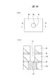
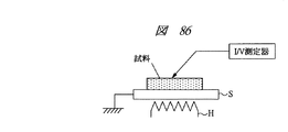
1.TDDB(Time Dependence on Dielectric Breakdown)寿命とは、所定の温度(たとえば140℃)の測定条件下で電極間に比較的高い電圧を加え、電圧印加から絶縁破壊までの時間を印加電界に対してプロットしたグラフを作成し、このグラフから実際の使用電界強度(たとえば0.2MV/cm)に外挿して求めた時間(寿命)をいう。図85は、本願のTDDB寿命測定に使用した試料を示し、(a)は平面図、(b)および(c)は(a)におけるB−B’線断面およびC−C’線断面を各々示す。この試料は実際には半導体ウエハのTEG(Test Equipment Group)領域に形成できる。図示するように一対の櫛形配線Lを第2配線層M2に形成し、最上層のパットP1,P2に各々接続する。この櫛形配線L間に電界が印加され電流が測定される。パットP1,P2は測定端子である。櫛形配線Lの配線幅、配線間隔、配線厚さは何れも0.5μmである。また配線対向長は1.58×105μmとした。図86は、測定の概要を示した概念図である。試料は測定ステージSに保持され、パッドP1,P2間に電流電圧測定器(I/V測定器)を接続する。試料ステージSはヒータHで加熱され試料温度が140℃に調整される。図87は電流電圧測定結果の一例である。試料温度140℃、電界強度5MV/cmの場合を例示した。TDDB寿命測定には定電圧ストレス法と低電流ストレス法とがあるが、本願では絶縁膜に印加される平均電界が一定となる定電圧ストレス法を用いている。電圧印加の後、時間の経過とともに電流密度は減少し、その後急激な電流増加(絶縁破壊)が観測される。ここでは、リーク電流密度が1μA/cm2に達した時間をTDDB寿命(5MV/cmにおけるTDDB寿命)とした。なお、本願において、TDDB寿命とは、特に言及しない限り0.2MV/cmにおける破壊時間(寿命)をいうが、広義には所定の電界強度に言及したうえで破壊までの時間としてTDDB寿命の語を用いる場合もある。また、特に言及しない限り、TDDB寿命は、試料温度140℃の場合をいう。なお、TDDB寿命は前記の櫛形配線Lで測定した場合をいうが、実際の配線間の破壊寿命を反映することはいうまでもない。 1. TDDB (Time Dependence on Dielectric Breakdown) life is a plot of the time from voltage application to dielectric breakdown against the applied electric field when a relatively high voltage is applied between the electrodes under a given temperature (eg 140 ° C) measurement condition. The time (life) obtained by creating an extrapolated graph and extrapolating from this graph to the actual electric field strength used (for example, 0.2 MV / cm). FIG. 85 shows a sample used for the TDDB lifetime measurement of the present application, (a) is a plan view, (b) and (c) are a BB ′ line cross section and a CC ′ line cross section in (a), respectively. Show. This sample can actually be formed in a TEG (Test Equipment Group) region of a semiconductor wafer. As shown in the figure, a pair of comb-shaped wirings L is formed in the second wiring layer M2 and connected to the uppermost pads P1 and P2. An electric field is applied between the comb-shaped wires L, and a current is measured. Pads P1 and P2 are measurement terminals. The wiring width, the wiring interval, and the wiring thickness of the comb-shaped wiring L are all 0.5 μm. The wiring facing length was 1.58 × 10 5 μm. FIG. 86 is a conceptual diagram showing an outline of measurement. The sample is held on the measurement stage S, and a current / voltage measuring device (I / V measuring device) is connected between the pads P1 and P2. The sample stage S is heated by the heater H, and the sample temperature is adjusted to 140 ° C. FIG. 87 shows an example of the current-voltage measurement result. A case where the sample temperature is 140 ° C. and the electric field strength is 5 MV / cm is illustrated. The TDDB lifetime measurement includes a constant voltage stress method and a low current stress method. In this application, the constant voltage stress method is used in which the average electric field applied to the insulating film is constant. After voltage application, the current density decreases with time, and then a rapid current increase (dielectric breakdown) is observed. Here, the time when the leakage current density reached 1 μA / cm 2 was defined as the TDDB life (TDDB life at 5 MV / cm). In the present application, the TDDB life means a breakdown time (life) at 0.2 MV / cm unless otherwise specified, but in a broad sense, after referring to a predetermined electric field strength, the term “TDDB life” is used as the time until breakdown. May be used. Unless otherwise specified, the TDDB lifetime refers to the case where the sample temperature is 140 ° C. Although the TDDB life is measured with the above-mentioned comb-shaped wiring L, it goes without saying that it actually reflects the breakdown life between the wirings.
2.プラズマ処理とは、プラズマ状態にある環境に基板表面、あるいは、基板上に絶縁膜、金属膜等の部材が形成されている時にはその部材表面を暴露し、プラズマの化学的、機械的(ボンバードメント)作用を表面に与えて処理することをいう。一般にプラズマは特定のガス(処理ガス)に置換した反応室内に必要に応じて処理ガスを補充しつつ、高周波電界等の作用によりガスを電離させて生成するが、現実には完全に処理ガスで置換することはできない。よって、本願では、たとえばアンモニアプラズマと称しても、完全なアンモニアプラズマを意図するものではなく、そのプラズマ内に含まれる不純物ガス(窒素、酸素、二酸化炭素、水蒸気等)の存在を排除するものではない。同様に、言うまでもないことであるが、プラズマ中に他の希釈ガスや添加ガスを含むことを排除するものではない。 2. Plasma treatment means that the surface of a substrate or the surface of a member such as an insulating film or metal film is exposed to an environment in a plasma state and exposed to the chemical and mechanical (bombardment) of the plasma. ) Refers to the treatment by applying an action to the surface. In general, plasma is generated by ionizing a gas by the action of a high-frequency electric field while replenishing the processing gas as needed in a reaction chamber substituted with a specific gas (processing gas). It cannot be replaced. Therefore, in this application, for example, ammonia plasma is not intended to be complete ammonia plasma, but does not exclude the presence of impurity gases (nitrogen, oxygen, carbon dioxide, water vapor, etc.) contained in the plasma. Absent. Similarly, it goes without saying that the inclusion of other dilution gas or additive gas in the plasma is not excluded.
還元性雰囲気のプラズマとは、還元作用、すなわち、酸素を引き抜く作用を有するラジカル、イオン、原子、分子等の反応種が支配的に存在するプラズマ環境をいい、ラジカル、イオンには、原子あるいは分子状のラジカルあるいはイオンが含まれる。また、環境内には単一の反応種のみならず、複数種の反応種が含まれていても良い。たとえば水素ラジカルとNH2ラジカルとが同時に存在する環境でもよい。
Plasma in a reducing atmosphere refers to a plasma environment in which reactive species such as radicals, ions, atoms, and molecules having a reducing action, that is, an action of extracting oxygen, exist predominantly. In the form of radicals or ions. In addition, the environment may contain not only a single reactive species but also a plurality of reactive species. For example, an environment in which hydrogen radicals and
3.本願でガスの濃度という場合には、質量流量における流量比を言うものとする。すなわち、ガスAとガスBとの混合ガスにおいて、ガスAの濃度が5%という時には、ガスAの質量流量をFa、ガスBの質量流量をFbとして、Fa/(Fa+Fb)=0.05のことをいう。 3. In the present application, the gas concentration refers to the flow rate ratio in the mass flow rate. That is, in the mixed gas of gas A and gas B, when the concentration of gas A is 5%, the mass flow rate of gas A is Fa, the mass flow rate of gas B is Fb, and Fa / (Fa + Fb) = 0.05 That means.
4.化学機械研磨(CMP)とは、一般に被研磨面を相対的に軟らかい布様のシート材料などからなる研磨パッドに接触させた状態で、スラリを供給しながら面方向に相対移動させて研磨を行うことをいい、本願においてはその他、被研磨面を硬質の砥石面に対して相対移動させることによって研磨を行うCML(Chemical Mechanical Lapping)、その他の固定砥粒を使用するもの、及び砥粒を使用しない砥粒フリーCMPなども含むものとする。 4). Chemical mechanical polishing (CMP) is generally performed by moving the surface to be polished in contact with a polishing pad made of a relatively soft cloth-like sheet material or the like while moving the surface relatively while supplying slurry. In this application, in addition, CML (Chemical Mechanical Lapping) for polishing by moving the surface to be polished relative to the hard grindstone surface, using other fixed abrasive grains, and using abrasive grains Including non-abrasive-free CMP.
砥粒フリー化学機械研磨は、一般に砥粒の重量濃度が0.5%以下のスラリを用いた化学機械研磨をいい、有砥粒化学機械研磨とは、砥粒の重量濃度が0.5%よりも高濃度のスラリを用いた化学機械研磨をいう。しかし、これらは相対的なものであり、第1ステップの研磨が砥粒フリー化学機械研磨で、それに続く第2ステップの研磨が有砥粒化学機械研磨である場合、第1ステップの研磨濃度が第2ステップの研磨濃度よりも1桁以上、望ましくは2桁以上小さい場合などには、この第1ステップの研磨を砥粒フリー化学機械研磨という場合もある。本明細書中において、砥粒フリー化学機械研磨と言うときは、対象とする金属膜の単位平坦化プロセス全体を砥粒フリー化学機械研磨で行う場合の他、主要プロセスを砥粒フリー化学機械研磨で行い、副次的なプロセスを有砥粒化学機械研磨で行う場合も含むものとする。 Abrasive-free chemical mechanical polishing generally refers to chemical mechanical polishing using a slurry having an abrasive weight concentration of 0.5% or less. Abrasive chemical mechanical polishing is an abrasive weight concentration of 0.5%. This refers to chemical mechanical polishing using a higher concentration of slurry. However, these are relative, and when the polishing in the first step is abrasive-free chemical mechanical polishing and the subsequent polishing in the second step is abrasive chemical mechanical polishing, the polishing concentration in the first step is If the polishing concentration in the second step is one digit or more, preferably two digits or less, the first step polishing may be referred to as abrasive-free chemical mechanical polishing. In this specification, the term “abrasive-free chemical mechanical polishing” refers to the case where the entire unit flattening process of the target metal film is performed by abrasive-free chemical mechanical polishing, and the main process is abrasive-free chemical mechanical polishing. This includes the case where the secondary process is carried out by abrasive chemical mechanical polishing.
5.研磨液(スラリ)とは、一般に化学エッチング薬剤に研磨砥粒を混合した懸濁液をいい、本願においては発明の性質上、研磨砥粒が混合されていないものを含むものとする。 5. The polishing liquid (slurry) generally refers to a suspension in which abrasive grains are mixed with a chemical etching agent. In the present application, a slurry in which abrasive grains are not mixed is included in the nature of the invention.
また、砥粒(スラリ粒子)とは、一般にスラリに含まれるアルミナ、シリカなどの粉末をいう。 Abrasive grains (slurry particles) generally refer to powders such as alumina and silica contained in the slurry.
6.防食剤とは、金属の表面に耐食性、疎水性あるいはその両方の性質を有する保護膜を形成することによって、CMPによる研磨の進行を阻止または抑制する薬剤をいい、一般にベンゾトリアゾール(BTA)などが使用される(詳しくは特開平8−64594号公報参照)。 6). The anticorrosive agent is an agent that prevents or suppresses the progress of polishing by CMP by forming a protective film having corrosion resistance and / or hydrophobic properties on the surface of the metal. Generally, benzotriazole (BTA) and the like are used. Used (refer to Japanese Patent Laid-Open No. 8-64594 for details).
7.導電性バリア膜とは、一般に銅が層間絶縁膜内や下層へ拡散するのを防止するために、埋め込み配線の側面または底面に比較的薄く形成される拡散バリア性の導電膜であり、一般に、窒化チタン(TiN)、タンタル(Ta)、窒化タンタル(TaN)等のような高融点金属またはその窒化物等が使用される。 7. The conductive barrier film is a diffusion barrier conductive film that is formed relatively thin on the side surface or bottom surface of the embedded wiring in order to prevent copper from diffusing into the interlayer insulating film or the lower layer. A refractory metal such as titanium nitride (TiN), tantalum (Ta), tantalum nitride (TaN), or a nitride thereof is used.
8.埋め込み配線または埋め込みメタル配線とは、一般にシングルダマシン(single damascene)やデュアルダマシン(dual damascene)などのように、絶縁膜に形成された溝などの内部に導電膜を埋め込んだ後、絶縁膜上の不要な導電膜を除去する配線形成技術によってパターニングされた配線をいう。また、一般に、シングルダマシンとは、プラグメタルと、配線用メタルとの2段階に分けて埋め込む、埋め込み配線プロセスを言う。同様にデュアルダマシンとは、一般にプラグメタルと、配線用メタルとを一度に埋め込む、埋め込み配線プロセスを言う。一般に、銅埋め込み配線を多層構成で使用されることが多い。 8). A buried wiring or a buried metal wiring is generally a single damascene or dual damascene or the like, after a conductive film is embedded in a trench formed in an insulating film and then on the insulating film. A wiring patterned by a wiring forming technique for removing an unnecessary conductive film. In general, single damascene refers to an embedded wiring process in which plug metal and wiring metal are embedded in two stages. Similarly, dual damascene generally refers to an embedded wiring process in which plug metal and wiring metal are embedded at once. In general, copper embedded wiring is often used in a multilayer configuration.
9.選択的除去、選択的研磨、選択的エッチング、選択的化学機械研磨というときは、いずれも選択比が5以上のものをいう。 9. The terms selective removal, selective polishing, selective etching, and selective chemical mechanical polishing all refer to those having a selection ratio of 5 or more.
10.選択比について、「AのBに対する」(または「Bに対するAの」)選択比がXというときは、研磨レートを例にとった場合、Bに対する研磨レートを基準にしてAに対する研磨レートを計算したときにXになることをいう。 10. As for the selection ratio, when the selection ratio “A to B” (or “A to B”) is X, the polishing rate for A is calculated based on the polishing rate for B when the polishing rate is taken as an example. It means to become X when you do.
11.本願において半導体集積回路装置というときは、特に単結晶シリコン基板上に作られるものだけでなく、特にそうでない旨が明示された場合を除き、SOI(Silicon On Insulator)基板やTFT(Thin Film Transistor)液晶製造用基板などといった他の基板上に作られるものを含むものとする。また、ウエハとは半導体集積回路装置の製造に用いる単結晶シリコン基板(一般にほぼ円盤形)、SOS基板、ガラス基板その他の絶縁、半絶縁または半導体基板などやそれらを複合した基板をいう。 11. In the present application, the term “semiconductor integrated circuit device” refers not only to a device manufactured on a single crystal silicon substrate, but also to an SOI (Silicon On Insulator) substrate or TFT (Thin Film Transistor) unless otherwise specified. It shall include those made on other substrates such as substrates for liquid crystal manufacturing. A wafer refers to a single crystal silicon substrate (generally substantially disk-shaped), an SOS substrate, a glass substrate, other insulating, semi-insulating or semiconductor substrates used in the manufacture of a semiconductor integrated circuit device, or a composite substrate thereof.
12.半導体集積回路ウエハ(半導体集積回路基板)または半導体ウエハ(半導体基板)とは、半導体集積回路の製造に用いるシリコンその他の半導体単結晶基板(一般にほぼ平面円形状)、サファイア基板、ガラス基板、その他の絶縁、反絶縁または半導体基板等並びにそれらの複合的基板を言う。なお、基板表面の一部または全部あるいはゲート電極の全部または一部を他の半導体、例えばSiGe等で形成しても良い。 12 A semiconductor integrated circuit wafer (semiconductor integrated circuit substrate) or a semiconductor wafer (semiconductor substrate) is a silicon or other semiconductor single crystal substrate (generally a substantially planar circular shape), sapphire substrate, glass substrate, etc. An insulating, anti-insulating or semiconductor substrate or the like and a composite substrate thereof. Note that part or all of the substrate surface or all or part of the gate electrode may be formed of another semiconductor such as SiGe.
また、半導体集積回路チップ(半導体集積回路基板)または半導体チップ(半導体基板)とは、ウエハ工程が完了した半導体ウエハを単位回路群に分割したものを言う。 A semiconductor integrated circuit chip (semiconductor integrated circuit substrate) or a semiconductor chip (semiconductor substrate) refers to a semiconductor wafer that has been subjected to a wafer process divided into unit circuit groups.
13.シリコンナイトライド、窒化ケイ素または窒化シリコン膜というときは、Si3N4のみではなく、シリコンの窒化物で類似組成の絶縁膜を含むものとする。 13. The term “silicon nitride, silicon nitride, or silicon nitride film” includes not only Si 3 N 4 but also an insulating film having a similar composition of silicon nitride.
14.キャップ膜は、埋め込み配線の情報の電気的接続部以外に形成される絶縁性および拡散バリア性の高い絶縁膜で、一般に層間絶縁膜の主要部とは別の材料、例えば窒化シリコン膜で形成される。 14 The cap film is an insulating film having a high insulating property and diffusion barrier property formed other than the electrical connection portion of the embedded wiring information, and is generally formed of a material different from the main part of the interlayer insulating film, for example, a silicon nitride film. The
15.ウエハプロセスとは、前工程とも呼ばれ、鏡面研磨ウエハ(ミラーウエハ)の状態から出発し、素子および配線形成工程を経て、表面保護膜を形成し、最終的にプローブにより電気的試験を行える状態にするまでの工程をいう。 15. Wafer process, also called pre-process, starts from the state of a mirror-polished wafer (mirror wafer), goes through the element and wiring formation process, forms a surface protection film, and finally can perform an electrical test with a probe This is the process up to.
16.導電性バリア膜の配線溝(凹部)または接続孔(凹部)内におけるカバレージは、サイドカバレージと、ボトムカバレージとを有している。図88は、絶縁膜60の上面およびその絶縁膜60に形成された配線溝61内に、バリア膜62をスパッタリング法で堆積した状態を模式的に示している。バリア膜のデポ膜厚という時は、一般的に絶縁膜60の上面上のバリア膜62の膜厚D1を言う。サイドカバレージは、配線溝61内の側壁部(側面と底面との交差部における角部も含む)におけるバリア膜62の被覆性をいい、その部分での膜厚D2が最も膜厚が薄くなる。また、ボトムカバレージは、配線溝61内の底面におけるバリア膜62の被覆性をいい、その部分での膜厚D3は上記デポ膜厚の次に厚くなる。例えば本発明者らの実験結果によれば、例えばアスペクト比が1の配線溝内に、バリア膜を指向性を特に考慮しない通常のスパッタリング法で堆積した場合においては、バリア膜のデポ膜厚が100nmで、サイドカバレージが30nm程度、ボトムカバレージが50nm程度であった。また、バリア膜をロングスロースパッタリング法により堆積した場合においては、バリア膜のデポ膜厚が100nmで、サイドカバレージが20nm程度、ボトムカバレージが90nm程度であった。
16. The coverage in the wiring groove (recess) or the connection hole (recess) of the conductive barrier film has side coverage and bottom coverage. FIG. 88 schematically shows a state in which a
17.ロングスロースパッタリング(Long Throw Sputtering)法とは、ボトムカバレージ向上の一方法であって、スパッタリング粒子の垂直成分だけを基板に到達させるため、ターゲットと基板との間の距離を離し、低圧で安定放電させるスパッタリング法を言う。 17. The Long Throw Sputtering method is a method for improving bottom coverage. Only the vertical component of the sputtered particles reaches the substrate, so the target and the substrate are separated from each other, and stable discharge is performed at low pressure. This refers to the sputtering method.
18.コリメートスパッタリング法は、アスペクト比の大きな配線溝や接続孔等のような凹部に成膜する際、底部まで充分な膜厚が得られるように、ターゲットと基板との間に格子状の板を挿入し、強制的に垂直成分を高める機構を有するスパッタリング法を言う。 18. The collimated sputtering method inserts a grid-like plate between the target and the substrate so that a sufficient film thickness can be obtained up to the bottom when forming a film in a recess such as a wiring groove or connection hole with a large aspect ratio. And a sputtering method having a mechanism for forcibly increasing the vertical component.
以下の実施の形態においては便宜上その必要があるときは、複数のセクションまたは実施の形態に分割して説明するが、特に明示した場合を除き、それらはお互いに無関係なものではなく、一方は他方の一部または全部の変形例、詳細、補足説明等の関係にある。 In the following embodiments, when it is necessary for the sake of convenience, the description will be divided into a plurality of sections or embodiments. However, unless otherwise specified, they are not irrelevant to each other. There are some or all of the modifications, details, supplementary explanations, and the like.
また、以下の実施の形態において、要素の数等(個数、数値、量、範囲等を含む)に言及する場合、特に明示した場合および原理的に明らかに特定の数に限定される場合等を除き、その特定の数に限定されるものではなく、特定の数以上でも以下でも良い。 Further, in the following embodiments, when referring to the number of elements (including the number, numerical value, quantity, range, etc.), especially when clearly indicated and when clearly limited to a specific number in principle, etc. Except, it is not limited to the specific number, and may be more or less than the specific number.
さらに、以下の実施の形態において、その構成要素(要素ステップ等も含む)は、特に明示した場合および原理的に明らかに必須であると考えられる場合等を除き、必ずしも必須のものではないことは言うまでもない。 Further, in the following embodiments, the constituent elements (including element steps and the like) are not necessarily indispensable unless otherwise specified and apparently essential in principle. Needless to say.
同様に、以下の実施の形態において、構成要素等の形状、位置関係等に言及するときは、特に明示した場合および原理的に明らかにそうでないと考えられる場合等を除き、実質的にその形状等に近似または類似するもの等を含むものとする。このことは、上記数値および範囲についても同様である。 Similarly, in the following embodiments, when referring to the shapes, positional relationships, etc. of the components, etc., the shapes are substantially the same unless otherwise specified, or otherwise apparent in principle. And the like are included. The same applies to the above numerical values and ranges.
また、実施の形態を説明するための全図において同一機能を有するものは同一の符号を付し、その繰り返しの説明は省略する。 Also, components having the same function are denoted by the same reference symbols throughout the drawings for describing the embodiments, and the repetitive description thereof is omitted.
また、本実施の形態においては、電界効果トランジスタを代表するMISFET(Metal Insulator Semiconductor Field Effect Transistor)を単にMISと略し、pチャネル型のMISFETをpMISと略し、nチャネル型のMISFETをnMISと略す。 In this embodiment, a MISFET (Metal Insulator Semiconductor Field Effect Transistor) representing a field effect transistor is simply abbreviated as MIS, a p-channel type MISFET is abbreviated as pMIS, and an n-channel type MISFET is abbreviated as nMIS.
(実施の形態1)
本実施の形態1においては、例えば本発明をCMOS(Complementary MOS)−LSI(Large Scale Integrated circuit)の製造方法に適用した場合を図1〜図19によって工程順に説明する。
(Embodiment 1)
In the first embodiment, for example, the case where the present invention is applied to a method of manufacturing a CMOS (Complementary MOS) -LSI (Large Scale Integrated circuit) will be described in the order of steps with reference to FIGS.
まず、図1に示すように、例えば1〜10Ωcm程度の比抵抗を有するp型の単結晶シリコンからなる半導体基板(以下、基板という)1に深さ350nm程度の素子分離溝2をフォトリソグラフィとドライエッチングを用いて形成した後、溝の内部を含む基板1上にCVD法で酸化シリコン膜3を堆積する。続いて溝の上部の酸化シリコン膜3を化学機械研磨(CMP)によってその表面を平坦化する。これにより、溝型の素子分離部2A(トレンチアイソレーション)を形成する。その後、基板1にp型不純物(ホウ素)およびn型不純物(例えばリン)をイオン打ち込みすることによって、p型ウエル4およびn型ウエル5を形成した後、基板1をスチーム酸化することによって、p型ウエル4およびn型ウエル5の表面に膜厚6nm程度のゲート絶縁膜6を形成する。なお、ここでいうゲート絶縁膜6の膜厚とは、二酸化シリコン換算膜厚であり、実際の膜厚と一致しない場合もある。
First, as shown in FIG. 1, an
ゲート絶縁膜6は、酸化シリコン膜に代えて酸窒化シリコン膜で構成しても良い。酸窒化シリコン膜は、酸化シリコン膜に比べて膜中における界面準位の発生を抑制したり、電子トラップを低減したりする効果が高いので、ゲート絶縁膜6のホットキャリア耐性を向上でき、絶縁耐性を向上させることができる。酸窒化シリコン膜を形成するには、例えば基板1をNO、NO2またはNH3といった含窒素ガス雰囲気中で熱処理すれば良い。また、p型ウエル4およびn型ウエル5のそれぞれの表面に酸化シリコンからなるゲート絶縁膜6を形成した後、基板1を上記した含窒素ガス雰囲気中で熱処理し、ゲート絶縁膜6と基板1との界面に窒素を偏析させることによっても、上記と同様の効果を得ることができる。
The
また、ゲート絶縁膜6を、例えば窒化シリコン膜あるいは酸化シリコン膜と窒化シリコン膜との複合絶縁膜で形成しても良い。酸化シリコンからなるゲート絶縁膜6を二酸化シリコン換算膜厚で5nm未満、特に3nm未満まで薄くすると、直接トンネル電流の発生やストレス起因のホットキャリア等による絶縁耐圧の低下が顕在化する。窒化シリコン膜は、酸化シリコン膜よりも誘電率が高いためにその二酸化シリコン換算膜厚は実際の膜厚よりも薄くなる。すなわち、窒化シリコン膜を有する場合には、物理的に厚くても、相対的に薄い二酸化シリコン膜と同等の容量を得ることができる。従って、ゲート絶縁膜6を単一の窒化シリコン膜あるいはそれと酸化シリコンとの複合膜で構成することにより、その実効膜厚を、酸化シリコン膜で構成されたゲート絶縁膜よりも厚くすることができるので、トンネル漏れ電流の発生やホットキャリアによる絶縁耐圧の低下を改善することができる。また、酸窒化シリコン膜は、酸化シリコン膜に比べて不純物が貫通し難いので、ゲート絶縁膜6を酸窒化シリコン膜で構成することにより、ゲート電極材料中の不純物が半導体基板側に拡散することに起因するしきい値電圧の変動を抑制することができる。
The
ここで、単一絶縁膜または複合絶縁膜の二酸化シリコン換算膜厚(以下、単に換算膜厚ともいう)drとは、対象となる絶縁膜の比誘電率をεi、その膜厚をdi、二酸化シリコンの比誘電率をεsとしたときに、次式で定義される膜厚である。 Here, the silicon dioxide equivalent film thickness (hereinafter also simply referred to as the equivalent film thickness) dr of the single insulating film or the composite insulating film is the relative dielectric constant εi of the target insulating film, the film thickness di, When the relative dielectric constant of silicon is εs, the film thickness is defined by the following equation.

例えば酸化シリコン(SiO2)および窒化シリコン(Si3N4)の誘電率は、それぞれ4〜4.2および8である。そこで、窒化シリコンの誘電率を酸化シリコンの誘電率の2倍として計算すると、例えば膜厚6nmの窒化シリコン膜の二酸化シリコン換算膜厚は3nmとなる。すなわち、膜厚6nmの窒化シリコン膜からなるゲート絶縁膜と膜厚3nmの酸化シリコン膜からなるゲート絶縁膜とは容量が等しい。また、膜厚2nmの酸化シリコン膜と膜厚2nmの窒化シリコン膜(換算膜厚=1nm)との複合膜からなるゲート絶縁膜の容量は、膜厚3nmの単一酸化シリコン膜からなるゲート絶縁膜の容量と同じである。 For example, the dielectric constants of silicon oxide (SiO 2 ) and silicon nitride (Si 3 N 4 ) are 4 to 4.2 and 8, respectively. Accordingly, when the dielectric constant of silicon nitride is calculated as twice the dielectric constant of silicon oxide, for example, the silicon nitride equivalent film thickness of a silicon nitride film having a film thickness of 6 nm is 3 nm. That is, the gate insulating film made of a silicon nitride film with a thickness of 6 nm and the gate insulating film made of a silicon oxide film with a thickness of 3 nm have the same capacitance. The capacitance of the gate insulating film made of a composite film of a silicon oxide film with a thickness of 2 nm and a silicon nitride film with a thickness of 2 nm (equivalent film thickness = 1 nm) is a gate insulation made of a single silicon oxide film with a thickness of 3 nm. It is the same as the capacity of the membrane.
次に、図2に示すように、ゲート絶縁膜6の上部に、低抵抗多結晶シリコン膜、WN(窒化タングステン)膜およびW(タングステン)膜からなるゲート電極7を形成する。多結晶シリコン膜はCVD法により、WN膜およびW膜はスパッタ法により形成できる。ゲート電極7は、これら堆積膜のパターニングにより形成する。ゲート電極7は、低抵抗多結晶シリコン膜上にWシリサイド膜またはコバルト(Co)シリサイド膜を堆積した積層膜などを使って形成しても良い。また、ゲート電極7の材料として多結晶または単結晶のシリコン(Si)とゲルマニウム(Ge)との合金を用いても良い。このようなゲート電極7を形成した後、イオン打ち込みすることによって、p型ウエル4に低不純物濃度のn−型半導体領域11を、n型ウエル5に低不純物濃度のp−型半導体領域12を形成する。
Next, as shown in FIG. 2, a
次に、図3に示すように、たとえば窒化シリコン膜をCVD法で堆積し、これを異方的にエッチングすることによって、ゲート電極7の側壁にサイドウォールスペーサ13を形成する。この後、イオン打ち込みすることによって、p型ウエル4に高不純物濃度のn+型半導体領域14(ソース、ドレイン)を形成し、n型ウエル5に高不純物濃度のp+型半導体領域15(ソース、ドレイン)を形成する。なお、n型不純物にはリンまたはヒ素を、p型不純物にはボロンを例示できる。その後、チタン、コバルト等の金属膜を堆積し、熱処理の後に未反応の金属膜を除去するいわゆるサリサイド法を用いて、n+型半導体領域14(ソース、ドレイン)の表面およびp+型半導体領域15(ソース、ドレイン)の表面にシリサイド層9を形成する。ここまでの工程で、nチャネル型MISFETQnおよびpチャネル型MISFETQpが完成する。
Next, as shown in FIG. 3, for example, a silicon nitride film is deposited by the CVD method, and this is anisotropically etched to form
次に、図4に示すように、基板1上にCVD法で酸化シリコン膜18を堆積し、続いてフォトレジスト膜をマスクにして酸化シリコン膜18をドライエッチングすることにより、n+型半導体領域14(ソース、ドレイン)の上部にコンタクトホール20を形成し、p+型半導体領域15(ソース、ドレイン)の上部にコンタクトホール21を形成する。またこのとき、ゲート電極7の上部にもコンタクトホール22を形成する。
Next, as shown in FIG. 4, a
酸化シリコン膜18は、ゲート電極7、7の狭いスペースを埋め込むことのできるリフロー性の高い膜、例えばBPSG(Boron-doped Phospho Silicate Glass)膜で構成する。また、スピン塗布法によって形成されるSOG(Spin On Glass) 膜で構成してもよい。
The
次に、コンタクトホール20、21、22の内部にプラグ23を形成する。プラグ23を形成するには、例えばコンタクトホール20、21、22の内部を含む酸化シリコン膜18の上部にCVD法でTiN膜およびW膜を堆積した後、酸化シリコン膜18の上部の不要なTiN膜およびW膜を化学機械研磨(CMP)法またはエッチバック法によって除去し、コンタクトホール20、21、22の内部のみにこれらの膜を残す。
Next, plugs 23 are formed inside the contact holes 20, 21, 22. In order to form the
次に、図5に示すように、酸化シリコン膜18の上部に第1層目の配線となるW配線24〜30を形成する。W配線24〜30を形成するには、例えば酸化シリコン膜18の上部にスパッタリング法でW膜を堆積した後、フォトレジスト膜をマスクにしてこのW膜をドライエッチングする。第1層目のW配線24〜30は、コンタクトホール20、21、22を通じてnチャネル型MISFETQnのソース、ドレイン(n+型半導体領域)、pチャネル型MISFETQpのソース、ドレイン(p+型半導体領域)あるいはゲート電極7と電気的に接続される。
Next, as shown in FIG. 5, W wirings 24 to 30 serving as first-layer wirings are formed on the
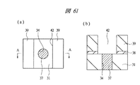
次に、図6(a)、(b)に示すように、第1層目のW配線24〜30の上部に酸化シリコン膜31を堆積し、続いてフォトレジスト膜をマスクにしたドライエッチングで酸化シリコン膜31にスルーホール32〜36を形成した後、スルーホール32〜36の内部にプラグ37を形成する。なお、図6(a)は半導体基板の主面の要部平面図、(b)は(a)のA−A線の断面図である。
Next, as shown in FIGS. 6A and 6B, a
酸化シリコン膜31は、例えばオゾン(または酸素)とテトラエトキシシラン(TEOS)とをソースガスに用いたプラズマCVD法で堆積する。また、プラグ37は、例えばW膜で構成し、前記コンタクトホール20、21、22の内部にプラグ23を形成した方法と同じ方法で形成する。
The
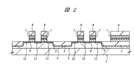
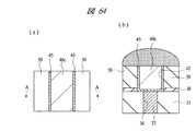
次に、図7(a)、(b)に示すように、酸化シリコン膜31の上部にプラズマCVD法で膜厚50nmの薄い窒化シリコン膜38を堆積し、続いて窒化シリコン膜38の上部にプラズマCVD法で膜厚450nm程度の酸化シリコン膜39を堆積する。その後、フォトレジスト膜をマスクにしたドライエッチングでスルーホール32〜36の上部の酸化シリコン膜39および窒化シリコン膜38を除去し、配線溝40〜44を形成する。なお、図7(a)は半導体基板の主面の要部平面図、(b)は(a)のA−A線の断面図である。
Next, as shown in FIGS. 7A and 7B, a thin
配線溝40〜44を形成するには、まず窒化シリコン膜38をエッチングストッパにして酸化シリコン膜39を選択的にエッチングし、その後、窒化シリコン膜38をエッチングする。このように、配線溝40〜44が形成される酸化シリコン膜39の下層に薄い窒化シリコン膜38を形成しておき、この窒化シリコン膜38の表面でエッチングを一旦停止した後、窒化シリコン膜38をエッチングすることにより、配線溝40〜44の掘り過ぎを生じることなく、その深さを精度良く制御することができる。
In order to form the
次に、上記配線溝40〜44の内部に以下のような方法で第2層目の配線となる埋め込みCu配線を形成する。
Next, a buried Cu wiring serving as a second-layer wiring is formed in the
まず、図8に示すように、配線溝40〜44の内部を含む酸化シリコン膜39の上部にスパッタリング法で、薄いTiN(窒化チタン)膜45を堆積した後、TiN膜45の上部に配線溝40〜44の深さよりも十分に厚い膜厚(例えば800nm程度)のCu膜46をスパッタリング法で堆積する。このTiN膜45およびCu膜46スパッタリング法としては、通常のスパッタリング法でも良いし、例えばロングスロースパッタリング法やコリメートスパッタリング法等のような指向性の高いスパッタリング法でも良い。
First, as shown in FIG. 8, a thin TiN (titanium nitride)
続いて、例えば475℃程度の非酸化性雰囲気(例えば水素雰囲気)中で基板1を熱処理することによってCu膜46をリフローさせ、配線溝40〜44の内部に隙間なくCu膜46を埋め込む。なお、ここでは、スパッタリング法によるCu膜46と、その後のリフローによる埋め込みを説明したが、薄いCu膜をスパッタリング法により形成し、その後、Cu膜46に相当する高純度のCu膜をメッキ法で形成しても良い。
Subsequently, the
TiN膜45は、Cuの拡散を防止する機能を有している。また、TiN膜45は、Cu膜46と酸化シリコン膜39との密着性を向上させる機能を有している。さらに、TiN膜45は、上記Cu膜46のリフロー時にCu膜46の濡れ性を向上させる機能を有している。
The
本実施の形態1においては、TiN膜45の最も厚い部分の厚さが50nmの場合を例示するが、本発明者らの検討結果によれば、このTiN膜45をさらに薄く、または、無くすこともできることが判明した。これについては、後の実施の形態6以降において説明する。
In the first embodiment, the case where the thickness of the thickest portion of the
このような機能を有する膜としては、TiNに代えて、Cuと殆ど反応しないWN、TaN(窒化タンタル)などの高融点金属窒化物を用いることが好ましい。また、そのTiNに代えて、高融点金属窒化物にSi(シリコン)を添加した材料や、Cuと反応し難いTa、Ti、W、TiW合金などの高融点金属を用いることもできる。 As a film having such a function, it is preferable to use refractory metal nitrides such as WN and TaN (tantalum nitride) that hardly react with Cu instead of TiN. Further, instead of TiN, a material obtained by adding Si (silicon) to a refractory metal nitride, or a refractory metal such as Ta, Ti, W, or TiW alloy that hardly reacts with Cu can be used.
次に、このようなCu膜46およびTiN膜45を上記CMP法等によって研磨する。この研磨工程に使用するCMP装置の全体構成の一例を図9に示す。
Next, the
このCMP装置100は、上記Cu膜46の研磨に用いる枚葉式のCMP装置であり、表面にCu膜46が形成された基板1を複数枚収容するローダ120、Cu膜46を研磨、平坦化する研磨処理部130、研磨が終了した基板1の表面に防蝕処理を施す防蝕処理部140、防蝕処理が終了した基板1を後洗浄するまでの間、その表面が乾燥しないように維持しておく浸漬処理部150、防蝕処理が終了した基板1を後洗浄する後洗浄処理部160および後洗浄が終了した基板1を複数枚収容するアンローダ170を備えている。
The
図10に示すように、CMP装置100の研磨処理部130は、上部が開口された筐体101を有しており、この筐体101に取り付けられた回転軸102の上端部には、モータ103によって回転駆動される研磨盤(プラテン)104が取り付けられている。この研磨盤104の表面には、多数の気孔を有する合成樹脂を均一に貼り付けて形成した研磨パッド105が取り付けられている。
As shown in FIG. 10, the polishing
また、この研磨処理部130は、基板1を保持するためのウエハキャリア106を備えている。ウエハキャリア106を取り付けた駆動軸107は、ウエハキャリア106と一体となってモータ(図示せず)により回転駆動され、かつ研磨盤104の上方で上下動されるようになっている。
In addition, the polishing
基板1は、ウエハキャリア106に設けられた真空吸着機構(図示せず)により、その主面すなわち被研磨面を下向きとしてウエハキャリア106に保持される。ウエハキャリア106の下端部には、基板1が収容される凹部106aが形成されており、この凹部106a内に基板1を収容すると、その被研磨面がウエハキャリア106の下端面とほぼ同一か僅かに突出した状態となる。
The
研磨盤104の上方には、研磨パッド105の表面と基板1の被研磨面との間に研磨スラリ(S)を供給するためのスラリ供給管108が設けられており、その下端から供給される研磨スラリ(S)によって基板1の被研磨面が化学的および機械的に研磨される。研磨スラリ(S)としては、例えばアルミナなどの砥粒と過酸化水素水または硝酸第二鉄水溶液などの酸化剤とを主成分とし、これらを水に分散または溶解させたものが使用される。
Above the polishing
また、この研磨処理部130は、研磨パッド105の表面を整形(ドレッシング)するための工具であるドレッサ109を備えている。このドレッサ109は、研磨盤104の上方で上下動する駆動軸110の下端部に取り付けられ、モータ(図示せず)により回転駆動されるようになっている。
Further, the polishing
研磨が終了した基板1は、防蝕処理部140において、その表面に防蝕処理が施される。防蝕処理部140は、上記した研磨処理部130の構成と類似した構成になっており、ここでは、まず研磨盤(プラテン)の表面に取り付けた研磨パッドに基板1の主面が押し付けられて研磨スラリが機械的に除去された後、例えばベンゾトリアゾール(BTA)などの防蝕剤を含んだ薬液が基板1の主面に供給されることによって、基板1の主面に形成されたCu配線の表面部分に疎水性保護膜が形成される。
The
研磨スラリの機械的洗浄(前洗浄)は、例えば図11に示すように、水平面内で回転させた基板1の両面をPVA(ポリビニルアルコール)のような合成樹脂の多孔質体からなる円筒状のブラシ121A、121Bで挟み、ブラシ121A、121Bを基板1の面に対して垂直な面内で回転しながら基板1の両面を同時に洗浄する。また、前洗浄後の防蝕処理に際しては、必要に応じて純水スクラブ洗浄、純水超音波洗浄、純水流水洗浄または純水スピン洗浄などを防蝕処理に先行または並行して行うことにより、研磨処理部130で基板1の主面に付着した研磨スラリ中の酸化剤を十分に除去し、酸化剤が実質的に作用しない条件下で疎水性の保護膜を形成するようにする。
For example, as shown in FIG. 11, mechanical polishing (pre-cleaning) of the polishing slurry is a cylindrical shape made of a porous body of a synthetic resin such as PVA (polyvinyl alcohol) on both sides of the
防蝕処理が終了した基板1は、その表面の乾燥を防ぐために、浸漬処理部150に一時的に保管される。浸漬処理部150は、防蝕処理が終了した基板1を後洗浄するまでの間、その表面が乾燥しないように維持するためのもので、例えば純水をオーバーフローさせた浸漬槽(ストッカ)の中に所定枚数の基板1を浸漬させて保管する構造になっている。このとき、Cu配線28〜30の電気化学的腐蝕反応が実質的に進行しない程度の低温に冷却した純水を浸漬槽に供給することにより、Cu配線28〜30の腐蝕をより一層確実に防止することができる。
The
基板1の乾燥防止は、例えば純水シャワーの供給など、少なくとも基板1の表面を湿潤状態に保持することのできる方法であれば、上記した浸漬槽中での保管以外の方法で行ってもよい。
Prevention of drying of the
後洗浄処理部160へ搬送された基板1は、その表面の湿潤状態が保たれた状態で直ちに後洗浄に付される。ここでは、酸化剤を中和するためにNH4 OHを含む洗浄液などの弱アルカリ薬液を供給しながら、基板1の表面をスクラブ洗浄(またはブラシ洗浄)した後、フッ酸水溶液を基板1の表面に供給してエッチングによる異物粒子(パーティクル)の除去を行う。また、上記のスクラブ洗浄に先行または並行して、基板1の表面を純水スクラブ洗浄、純水超音波洗浄、純水流水洗浄または純水スピン洗浄したり、基板1の裏面を純水スクラブ洗浄したりしてもよい。
The
上記後洗浄処理が終了した基板1は、純水リンスおよびスピンドライの後、乾燥した状態でアンローダ170に収容され、複数枚単位で一括して次工程へ搬送される。
The
なお、図12に示すように、防蝕処理が終了した基板1の表面乾燥を防ぐための浸漬処理部(ウエハ保管部)150を遮光構造にし、保管中の基板1の表面に照明光などが照射されないようにすることができる。これにより、光起電力効果による短絡電流の発生を防ぐようにできる。浸漬処理部150を遮光構造にするには、具体的には浸漬槽(ストッカ)の周囲を遮光シートなどで被覆することによって、浸漬槽(ストッカ)の内部の照度を少なくとも500ルクス以下、好ましくは300ルクス以下、さらに好ましくは100ルクス以下にする。
In addition, as shown in FIG. 12, the immersion process part (wafer storage part) 150 for preventing the surface drying of the board |
また、図13に示すように、研磨処理の直後、すなわちその表面に残った研磨スラリ中の酸化剤による電気化学的腐蝕反応が開始される前に直ちに乾燥処理部に搬送され、研磨スラリ中の水分が強制乾燥によって除去されてもよい。図13に示すCMP装置200は、表面にCu膜が形成された基板1を複数枚収容するローダ220、Cu膜を研磨、平坦化して配線を形成する研磨処理部230、研磨が終了した基板1の表面を乾燥させる乾燥処理部240、基板1を後洗浄する後洗浄処理部250および後洗浄が終了した基板1を複数枚収容するアンローダ260を備えている。このCMP装置200を使ったCu配線形成プロセスでは、研磨処理部230において研磨処理に付された基板1は、研磨処理の直後、すなわちその表面に残った研磨スラリ中の酸化剤による電気化学的腐蝕反応が開始される前に直ちに乾燥処理部240に搬送され、研磨スラリ中の水分が強制乾燥によって除去される。その後、基板1は、乾燥状態が維持されたまま後洗浄処理部250に搬送され、後洗浄処理に付された後、純水リンスおよびスピンドライを経てアンローダ260に収容される。この場合、研磨処理の直後から後洗浄が開始されるまでの間、基板1の表面が乾燥状態に保たれるために、電気化学的腐蝕反応の開始が抑制され、これにより、Cu配線の腐蝕を有効に防止することが可能となる。
Further, as shown in FIG. 13, immediately after the polishing process, that is, immediately before the electrochemical corrosion reaction by the oxidant in the polishing slurry remaining on the surface is started, it is immediately transferred to the drying processing unit, where the polishing slurry contains Moisture may be removed by forced drying. A
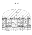
このようなCMP法による研磨工程を経て、酸化シリコン膜39上のCu膜46およびTiN膜45を除去し、図14に示すように、配線溝40〜44内にCu配線46a〜46eを形成する。
Through such a polishing process by the CMP method, the
次に、Cu配線46a〜46eと酸化シリコン膜39の表面にプラズマ処理を施す。図15は、プラズマ処理に用いる処理装置の一例を示した断面図(a)および平面図(b)である。なお、このプラズマ処理については、本願発明者などによる特願平11−226876号に記載されている。
Next, plasma processing is performed on the surfaces of the Cu wirings 46 a to 46 e and the
この処理装置には、ロードロック室301に2つの処理室302a,302bとカセットインタフェイス303が取り付けられている。ロードロック室301内には基板1を搬送するロボット304を有する。ロードロック室301と処理室302a,302bとの間には、処理中にもロードロック室301内の高真空状態が保てるようにゲートバルブ305を有する。
In this processing apparatus, two processing
処理室302a,302b内には基板1を保持するサセプタ306、ガス流を整えるバッフル板307、サセプタ306を支持する支持部材308、サセプタ306に対向して配置されるメッシュ状の電極309、バッフル板307にほぼ対向して配置された絶縁板310を有する。絶縁板310はサセプタ306と電極309の間以外の不必要な領域での寄生放電を抑制する作用がある。サセプタ306の裏面側には反射ユニット311内に設置されたランプ312が配置され、ランプ312を発した赤外線313が石英窓314を通過してサセプタ306および基板1に照射される。これにより基板1が加熱される。なお、基板1はサセプタ306上にフェイスアップで設置される。
In the
処理室302a,302bはその内部を高真空に排気することが可能であり、処理ガスおよび高周波電力がガスポート315から供給される。処理ガスはメッシュ状の電極309を通過して基板1の近傍に供給される。処理ガスは真空マニホールド316から排出され、処理ガスの供給流量および排気速度を制御することにより圧力が制御される。高周波電力は電極309に印加され、サセプタ306と電極309との間でプラズマを生成する。高周波電力はたとえば13.56MHzの周波数を用いる。
The inside of the
処理室302aでは、たとえば次に説明するアンモニアプラズマ処理が行われる。また、処理室302bでは、後に説明するキャップ膜(窒化シリコン膜)の堆積が行われる。処理室302aと処理室302bとはロードロック室301を介して接続されているため、アンモニアプラズマ処理の後に真空破壊することなく基板1を処理室302bに搬送することができ、アンモニアプラズマ処理とキャップ膜の形成を連続的に行うことができる。
In the
次に、上記したプラズマ処理装置を用いて、基板1にアンモニアプラズマ処理を施す。カセットインタフェイス303から基板1がロボット304によりロードロック室301に搬入される。ロードロック室301を十分な減圧状態になるまで真空排気し、ロボット304を用いて処理室302aに基板1を搬送する。処理室302aのゲートバルブ305を閉じ、処理室302a内が十分な真空度になるまで排気した後、処理室302aにアンモニアガスを導入し、圧力調整を行って所定の圧力に維持する。その後、高周波電源から電極309に電界を印加し、図16に示すように、基板1の表面をプラズマ処理する。所定時間の経過後高周波電界を停止し、プラズマを停止する。その後、処理室302a内を真空排気し、ゲートバルブ305を開いてロボット304により基板1をロードロック室301に搬出する。なお、ロードロック室301は高真空状態に維持されているため、基板1の表面が大気雰囲気に曝されることがない。
Next, ammonia plasma treatment is performed on the
プラズマ処理条件は、たとえば、基板1のサイズを8インチ(=20cm程度)とした場合、処理圧力を5.0Torr(=6.6661×10²Pa)、RF電力を600W、基板温度を400℃、アンモニア流量を200sccm、処理時間を10秒とすることができる。電極間距離は600milsとした。なお、プラズマ処理条件は、これら例示した条件に限られないのはもちろんである。本発明者らの検討では、圧力が高いほどプラズマダメージを低減でき、基板温度が高いほどTDDB寿命の基板内ばらつきの低減と長寿命化がはかれる。また、基板温度が高く、RF電力が大きく、処理時間が長いほどCuの表面にヒロックが発生しやすい、という知見が得られている。これらの知見と装置構成による条件のばらつきを考慮すると、処理圧力は0.5〜6Torr(=0.66661×10²〜7.99932×10²Pa)、RF電力は300〜600W、基板温度は350〜450℃、アンモニア流量は20〜500sccm、処理時間は5〜180秒、電極間距離は300〜600milsの範囲で設定することができる。
As for the plasma processing conditions, for example, when the size of the
このように、Cu配線46a〜46eと酸化シリコン膜39の表面にプラズマ処理を施すことにより、Cu配線46a〜46eおよび酸化シリコン膜39の表面のごく薄い領域に各々の下地材料の窒化膜を形成することができる。これにより、次に説明するキャップ膜(窒化シリコン膜)とCu配線46a〜46eおよび酸化シリコン膜39との密着性が向上し、TDDB寿命を著しく向上できる。この点は、本発明者らの実験結果の解析とともに後に詳しく説明する。
In this way, by performing plasma treatment on the surfaces of the Cu wirings 46 a to 46 e and the
次に、ロボット304を用いて基板1を処理室302bに搬送する。処理室302bのゲートバルブ305を閉じ、処理室302b内が十分な真空度になるまで排気した後、処理室302bにシラン(SiH4 )、アンモニア、窒素の混合ガスを導入し、圧力調整を行って所定の圧力に維持する。その後、高周波電源から電極309に電界を印加してプラズマを発生し、図17に示すように、Cu配線46a〜46eおよび酸化シリコン膜39の表面に窒化シリコン膜47(キャップ膜)を堆積する。所定時間の経過後高周波電界を停止しプラズマを停止する。その後、処理室302b内を真空排気し、ゲートバルブ305を開いてロボット304により基板1をロードロック室301に搬出する。さらに、ロボット304を用いてカセットインタフェイス303に基板1を排出する。
Next, the
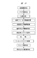
窒化シリコン膜47の膜厚は、たとえば50nmとする。その後、第3層目の配線と第2層目の配線(Cu配線46a〜46e)とを接続するプラグを形成するための酸化シリコン膜を形成し、前記したのと同様の方法で、第3層目以降の埋め込みCu配線が形成される。図18は、上述したCu配線46a〜46eの形成プロセスの全体フロー図である。
The film thickness of the
図19に第7層目の配線までを形成したCMOS−LSIの一例を示す。第1層目の配線(M1)は、前記した通りタングステン膜からなる。第1層目の配線の膜厚および配線ピッチ(隣接配線の中心から中心までの距離)は、例えば0.4μm程度または0.25μm程度である。 FIG. 19 shows an example of a CMOS-LSI in which the wiring up to the seventh layer is formed. The first layer wiring (M1) is made of a tungsten film as described above. The film thickness and the wiring pitch of the first layer wiring (distance from the center of the adjacent wiring to the center) are, for example, about 0.4 μm or about 0.25 μm.
また、第2層配線(M2)から第5層配線(M5)までは、前記したCu配線の形成方法で製造する。第2層配線(M2)および第3層配線(M3)のTiN膜の厚さは、例えば0.05μm程度、Cu膜の厚さは、例えば0.35μm程度、配線幅および配線ピッチは、例えば0.5μm程度または0.25μm程度である。第4層配線(M4)および第5層配線(M5)のTiN膜の厚さは、例えば0.05μm程度、Cu膜の厚さは、例えば0.95μm程度、配線幅および配線ピッチは、例えば1.0μm程度または0.25μm程度である。 The second layer wiring (M2) to the fifth layer wiring (M5) are manufactured by the above-described Cu wiring forming method. The thickness of the TiN film of the second layer wiring (M2) and the third layer wiring (M3) is, for example, about 0.05 μm, the thickness of the Cu film is, for example, about 0.35 μm, and the wiring width and wiring pitch are, for example, It is about 0.5 μm or about 0.25 μm. The thickness of the TiN film of the fourth layer wiring (M4) and the fifth layer wiring (M5) is, for example, about 0.05 μm, the thickness of the Cu film is, for example, about 0.95 μm, and the wiring width and wiring pitch are, for example, It is about 1.0 μm or about 0.25 μm.
また、第6層配線(M6)は、例えばタングステン膜、アルミニウム膜およびタングステン膜の3層構成とされている。また、第7層配線(M7)は、例えばアルミニウム膜からなる。第7層配線(M7)のパッドには、バンプ電極が形成される、またはボンディングワイヤが接続されるが図示を省略している。なお、第7層配線(M7)をアルミニウムとタングステンとの積層膜で構成している理由の1つのとして、その積層膜は、ダマシン配線構造を採用しない通常の半導体集積回路装置の最上層に使用しており、バンプ電極やボンディングワイヤとの接続上の信頼性を確保できることが経験的に実証されているからである。 The sixth layer wiring (M6) has a three-layer structure of, for example, a tungsten film, an aluminum film, and a tungsten film. The seventh layer wiring (M7) is made of, for example, an aluminum film. A bump electrode or a bonding wire is connected to the pad of the seventh layer wiring (M7), but the illustration is omitted. As one of the reasons why the seventh layer wiring (M7) is composed of a laminated film of aluminum and tungsten, the laminated film is used as the uppermost layer of a normal semiconductor integrated circuit device that does not employ a damascene wiring structure. This is because it has been empirically proved that reliability in connection with bump electrodes and bonding wires can be secured.
第1層配線M1と第2層配線M2とを接続するスルーホールの直径は、例えば0.45μm程度または0.25μm程度である。第2層配線M2と第3層配線M3とを接続するスルーホールの直径は、例えば0.5μm程度または0.25μm程度である。第3層配線M3と第4層配線M4とを接続するスルーホールの直径は、例えば0.5μm程度または0.25μm程度である。第4層配線M4と第5層配線M5とを接続するスルーホールの直径は、例えば1.0μm程度または0.25μm程度である。第5層配線M5と第6層配線M6とを接続するスルーホールの直径は、例えば0.5μm程度または0.25μm程度である。 The diameter of the through hole connecting the first layer wiring M1 and the second layer wiring M2 is, for example, about 0.45 μm or about 0.25 μm. The diameter of the through hole connecting the second layer wiring M2 and the third layer wiring M3 is, for example, about 0.5 μm or about 0.25 μm. The diameter of the through hole connecting the third layer wiring M3 and the fourth layer wiring M4 is, for example, about 0.5 μm or about 0.25 μm. The diameter of the through hole connecting the fourth layer wiring M4 and the fifth layer wiring M5 is, for example, about 1.0 μm or about 0.25 μm. The diameter of the through hole connecting the fifth layer wiring M5 and the sixth layer wiring M6 is, for example, about 0.5 μm or about 0.25 μm.
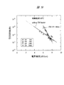
本実施の形態によれば、TDDB寿命が大幅に改善される。図20は、本実施の形態の第2層配線M2(Cu配線46a〜46e)と同層に形成されたTEGサンプルのTDDB寿命を示すグラフであり、本実施の形態の場合のデータをラインAに示す。比較のためにアンモニアプラズマ処理をしない場合のTDDB寿命データ(ラインRef)も同時に示す。図から明らかな通り、本実施の形態では、比較データと比べて約6桁の寿命向上が見られる。 According to the present embodiment, the TDDB life is significantly improved. FIG. 20 is a graph showing the TDDB life of the TEG sample formed in the same layer as the second layer wiring M2 (Cu wirings 46a to 46e) of the present embodiment. Shown in For comparison, TDDB life data (line Ref) when ammonia plasma treatment is not performed are also shown. As is apparent from the figure, in this embodiment, the life is improved by about 6 digits compared to the comparison data.
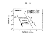
図21は、本実施の形態で適用した酸化シリコン膜39をそれよりも緻密で強固な窒化シリコン膜に置き換えた場合のデータ(ラインB)を示す。絶縁膜を窒化シリコンに置き換えた場合であってもアンモニアプラズマ処理を施さなければ絶縁膜を酸化シリコン膜とした場合と何ら相違はない(ラインRef)。一方、窒化シリコン膜を絶縁膜に適用し、アンモニアプラズマ処理を施せば、本実施の形態以上にTDDB寿命が向上する。しかし、その向上の割合は大きくなく、アンモニアプラズマ処理を行うことによる要因の方が支配的であることがわかる。これは、TDDB寿命を支配する要因は絶縁膜のバルクよりは、その界面が支配的であることを示している。
FIG. 21 shows data (line B) when the
そこで、本発明者らは、アンモニアプラズマ処理によりTDDB寿命が向上する機構を解析するために銅と酸化シリコン膜の表面分析を行った。以下に解析の結果を説明する。 Therefore, the present inventors conducted surface analysis of copper and silicon oxide films in order to analyze the mechanism by which the TDDB life is improved by the ammonia plasma treatment. The results of the analysis will be described below.
図22〜図24は、Cu配線表面のXPS(X-ray Photo-electron Spectroscopy )分析の結果を示したグラフである。各図の(a)、(c)はCu2pの分光結果を示し、(b)、(d)はN1sの分光結果を示す。 22 to 24 are graphs showing the results of XPS (X-ray Photo-electron Spectroscopy) analysis of the Cu wiring surface. In each figure, (a) and (c) show the spectral results of Cu2p, and (b) and (d) show the spectral results of N1s.
図22(a)、(b)はアズデポ状態のCu膜表面を分析した結果である。Cu2pのピークが観察され、N1sのピークはノイズレベルであることから、アズデポ状態のCu膜には窒素は存在しないことがわかる。図22(c)、(d)は、Cu膜にCMPのみを施した直後のCu配線表面を分析した結果である。Cu2pのピークとともにN1sのピークが観察される。前記した通りスラリにはBTAが含まれるため、Cu表面に残留したBTA内の窒素を観察しているものと推察できる。図23(a)、(b)は、CMP後に後洗浄まで行った状態のCu配線表面を分析した結果である。Cu2pピークに変化は見られないが、N1sピークが低下している。洗浄によりBTAが除去されたと考えられる。図23(c)、(d)は、後洗浄後大気雰囲気に24時間放置した状態のCu配線表面を分析した結果である。Cu2pのピークとともにCuOのピークが観察される。N1sピークには放置による変化は見られない。放置によりCu表面が酸化され、CuOが生成していることがわかる。 FIGS. 22A and 22B show the results of analysis of the as-deposited Cu film surface. Since the Cu2p peak is observed and the N1s peak is a noise level, it can be seen that nitrogen is not present in the as-deposited Cu film. 22C and 22D show the results of analysis of the Cu wiring surface immediately after the CMP of the Cu film only. The N1s peak is observed together with the Cu2p peak. As described above, since BTA is contained in the slurry, it can be assumed that nitrogen in BTA remaining on the Cu surface is observed. FIGS. 23A and 23B show the results of analysis of the Cu wiring surface in a state where the post-cleaning is performed after the CMP. Although no change is observed in the Cu2p peak, the N1s peak is lowered. It is thought that BTA was removed by washing. 23 (c) and 23 (d) show the results of analysis of the Cu wiring surface in a state where it is left in the air atmosphere after post-cleaning for 24 hours. A CuO peak is observed together with a Cu2p peak. The N1s peak is not changed by standing. It can be seen that the Cu surface was oxidized by being left and CuO was produced.
このように酸化されたCu配線にアンモニアプラズマ処理を施した状態のCu配線表面を分析した結果が図24(a)、(b)である。CuOのピークはほぼ消失している。一方、N1sピークは強く生じている。Cu表面が還元されて酸素が引き抜かれているとともに表面が窒化されていると考えられる。比較のため、酸化されたCu配線に350℃の水素熱処理を施した状態のCu配線表面を分析した。結果は図24(c)、(d)である。Cu2pピークについて、図24(c)と図24(a)とを比較すれば、よりアズデポ状態(図22(a))に近いことから、水素熱処理の方が還元性は強いと考えられる。一方、N1sピークはほとんど観察されないことから、水素熱処理ではCu表面が還元されるのみである。 FIGS. 24A and 24B show results obtained by analyzing the surface of the Cu wiring in a state where the ammonia wiring is applied to the oxidized Cu wiring. The CuO peak has almost disappeared. On the other hand, the N1s peak is strongly generated. It is considered that the Cu surface is reduced and oxygen is extracted and the surface is nitrided. For comparison, the surface of the Cu wiring in a state where the oxidized Cu wiring was subjected to hydrogen heat treatment at 350 ° C. was analyzed. The results are shown in FIGS. 24 (c) and 24 (d). When the Cu2p peak is compared with FIG. 24C and FIG. 24A, it is closer to the as-deposited state (FIG. 22A), and therefore it is considered that the hydrogen heat treatment is more reducible. On the other hand, since almost no N1s peak is observed, the hydrogen heat treatment only reduces the Cu surface.
以上の結果から、アンモニアプラズマ処理によりCu配線46a〜46eの表面は還元されるとともに窒化層が形成されてことがわかる。この窒化層は、アンモニアプラズマ処理の後に窒化シリコン膜を堆積する際の原料ガスに含まれるシランと銅との反応を防止し、銅のシリサイドの形成を抑制する働きを有すると考えられる。シリサイド形成の防止は配線抵抗の増加を抑制する効果がある。
From the above results, it can be seen that the surfaces of the
図25は、酸化シリコン膜表面のXPS分析を行った結果を示すグラフであり、図26および図27は、酸化シリコン膜の質量分析(TDS−APIMS)を行った結果を示すグラフである。酸化シリコン膜の分析においては、CMP後に洗浄まで行った状態(プロファイルC)、CMP後洗浄後に水素プラズマ処理を行った状態(プロファイルD)、CMP後洗浄後にアンモニアプラズマ処理を行った状態(プロファイルE)、CMP後洗浄後に窒素プラズマ処理を行った状態(プロファイルF)について分析した。なお、プロファイルCの1eV程度の高エネルギー方向へのずれはチャージアップの影響によるものである。 FIG. 25 is a graph showing the results of XPS analysis of the silicon oxide film surface, and FIGS. 26 and 27 are graphs showing the results of mass analysis (TDS-APIMS) of the silicon oxide film. In the analysis of the silicon oxide film, the state after cleaning after CMP (profile C), the state after hydrogen cleaning after CMP (profile D), and the state after ammonia cleaning after cleaning after CMP (profile E) ), A state (profile F) in which nitrogen plasma treatment was performed after post-CMP cleaning was analyzed. Note that the shift of profile C in the high energy direction of about 1 eV is due to the effect of charge-up.
図25(a)、(b)はともにSi2pスペクトルを観察したデータであり、(a)は10nm程度の深さを、(b)は2nm程度の深さを分析したものである。図25(c)、(d)、(e)は各々N1s、O1s、C1sスペクトルを観察したデータである。 FIGS. 25A and 25B are data obtained by observing the Si2p spectrum. FIG. 25A shows the depth of about 10 nm, and FIG. 25B shows the depth of about 2 nm. 25 (c), (d), and (e) are data obtained by observing N1s, O1s, and C1s spectra, respectively.
図25(b)から、水素プラズマ処理(プロファイルD)の低エネルギー側(102eV付近)にブロードなピークが見られる。これはSi−H結合が存在すると考えられ、水素プラズマ処理により酸化シリコン膜表面にSi−Hが形成されると推察される。 FIG. 25B shows a broad peak on the low energy side (near 102 eV) of the hydrogen plasma treatment (profile D). This is considered that Si-H bonds exist, and it is assumed that Si-H is formed on the surface of the silicon oxide film by the hydrogen plasma treatment.
図25(a)から、アンモニアプラズマ処理(プロファイルE)と窒素プラズマ処理(プロファイルF)の105eVのピークが低エネルギー側に広がった非対称なピークになっている。非対称部分のピーク(103.5eV)はSi−O−N結合と考えられる。アンモニアプラズマ処理および窒素プラズマ処理により酸化シリコン膜の表面が窒化されていると推察される。また、図25(a)と(b)との比較から、窒化は表面でより強くされていると考えられる。アンモニアプラズマ処理および窒素プラズマ処理による窒化は、図25(c)でも確認できる。 From FIG. 25 (a), the 105 eV peak of the ammonia plasma treatment (profile E) and the nitrogen plasma treatment (profile F) is an asymmetric peak spreading toward the low energy side. The asymmetric peak (103.5 eV) is considered to be a Si—O—N bond. It is presumed that the surface of the silicon oxide film is nitrided by ammonia plasma treatment and nitrogen plasma treatment. Further, from the comparison between FIGS. 25A and 25B, it is considered that nitriding is strengthened on the surface. Nitridation by ammonia plasma treatment and nitrogen plasma treatment can also be confirmed in FIG.
図25(e)から、水素プラズマ処理(プロファイルD)では炭素はほとんど検出されない。水素プラズマ処理により表面の有機物が除去されていることがわかる。また、CMP後(プロファイルC)の289eVのピークはC−O結合と考えられる。CMP後ではスラリが残留していると考える。 From FIG. 25 (e), almost no carbon is detected in the hydrogen plasma treatment (profile D). It can be seen that organic substances on the surface are removed by the hydrogen plasma treatment. Further, the peak at 289 eV after CMP (profile C) is considered to be a C—O bond. It is considered that slurry remains after CMP.
図25(f)は、SiピークとNピークとからそれらの存在比を求め、N量を推定した値を示す。アンモニアプラズマ処理と窒素プラズマ処理とではほぼ同等の窒化がなされていると考える。 FIG. 25 (f) shows a value obtained by obtaining the abundance ratio from the Si peak and the N peak and estimating the N amount. It is considered that almost the same nitriding is performed in the ammonia plasma treatment and the nitrogen plasma treatment.
図26(a)、(b)、(c)、(d)は各々質量数41(Ar−H)、質量数27(C2 H3 )、質量数57(C4 H9 )、質量数59(C3 H7 O)を測定したグラフである。また、図27(a)、(b)、(c)、(d)は各々質量数28(Si、C2 H4 )、質量数44(SiO、C3 H6)、質量数29(SiH、C2 H5 )、質量数31(SiH3 )を測定したグラフである。 26 (a), (b), (c), and (d) are mass numbers 41 (Ar-H), mass numbers 27 (C2 H3), mass numbers 57 (C4 H9), and mass numbers 59 (C3 H7). It is the graph which measured O). FIGS. 27 (a), (b), (c), and (d) are mass numbers 28 (Si, C2 H4), mass numbers 44 (SiO, C3 H6), and mass numbers 29 (SiH, C2 H5), respectively. FIG. 3 is a graph obtained by measuring a mass number 31 (SiH 3).
図26(a)から、プラズマ処理による水素の脱離量の相違はほとんどないが、水素プラズマ処理(プロファイルD)の脱離温度が他の場合(560℃)と比較して520℃と低いことがわかる。 From FIG. 26 (a), there is almost no difference in the amount of hydrogen desorbed by the plasma treatment, but the desorption temperature of the hydrogen plasma treatment (profile D) is as low as 520 ° C compared to the other cases (560 ° C). I understand.
図26(a)、(b)、(c)から、各プロセスとも有機物の離脱が見られる。一方、図27(a)〜(d)から、有機物の離脱以外のピークの存在が見られる。すなわち、300〜400℃のピークは各々、Si、SiO、SiH、SiH3 と思われる。各図を比較すると、水素、アンモニア、窒素の各プラズマ処理で、SiOの離脱は見られるが、アンモニアプラズマ処理ではSiH、SiH3 の離脱はほとんど観察されない。すなわち、アンモニアプラズマ処理ではSi−O−Nが形成され、比較的低いエネルギーで容易に離脱する。また、離脱に必要なエネルギーは窒素プラズマ処理の場合が最も高く、水素プラズマ処理とアンモニアプラズマ処理とではほぼ同じと言える。
26 (a), (b), and (c), organic substances are detached from each process. On the other hand, from FIGS. 27A to 27D, the presence of peaks other than the separation of organic substances can be seen. That is, the peaks at 300 to 400 ° C. are considered to be Si, SiO, SiH, and
これらの結果から、酸化シリコン膜表面のダングリングボンドの原因となるSi−OHやSi−O−は、アンモニアプラズマ処理により、弱い結合のSi−O−Nで終端されると考えられる。アンモニアプラズマ処理の後の窒化シリコン膜の成膜において、ごく表面のSi−O−Nが離脱し、バルクのSi−O結合と窒化シリコン膜のSi−Nとが強固に結合し、連続的な界面を形成する。これが界面の密着性を向上する機構と考えられる。一方、アンモニアプラズマ処理を行わない場合には、そもそもSi−OH結合の多い酸化シリコン膜の表面と窒化シリコン膜の原料ガスであるアンモニアとが縮合反応し、ダングリングボンドの原因であるSi−O−結合が多数発生していると考えられる。酸化シリコン膜と窒化シリコン膜との界面に多数のダングリングボンドが存在すれば、そこはリークパスを形成することとなり配線間のリーク電流、ひいては絶縁破壊の原因となっていると考えられる。 From these results, it is considered that Si—OH and Si—O— that cause dangling bonds on the surface of the silicon oxide film are terminated by weakly bonded Si—O—N by ammonia plasma treatment. In the film formation of the silicon nitride film after the ammonia plasma treatment, Si—O—N on the very surface is detached, and the bulk Si—O bond and the Si—N of the silicon nitride film are firmly bonded, and are continuously formed. Form an interface. This is considered to be a mechanism for improving the adhesion at the interface. On the other hand, when ammonia plasma treatment is not performed, the surface of the silicon oxide film having many Si—OH bonds and ammonia, which is a raw material gas for the silicon nitride film, undergo a condensation reaction, and Si—O, which is the cause of dangling bonds. -Many bonds are considered to have occurred. If there are a large number of dangling bonds at the interface between the silicon oxide film and the silicon nitride film, it forms a leak path, which is considered to cause a leakage current between wirings and, consequently, a dielectric breakdown.
以上の分析結果から、アンモニアプラズマ処理により、酸化されたCu配線の表面は還元されてCu単元素に変換され、イオン化されたCuよりも電気的に安定な状態になり、かつ、酸化シリコン膜/窒化シリコン膜界面は連続的な強固な膜になることから、リーク電流が減少し、TDDB寿命も大幅に向上すると考えられる。 From the above analysis results, the surface of the oxidized Cu wiring is reduced and converted into a Cu single element by the ammonia plasma treatment, and becomes electrically stable than the ionized Cu, and the silicon oxide film / Since the silicon nitride film interface becomes a continuous and strong film, it is considered that the leakage current is reduced and the TDDB life is greatly improved.
本発明者らはアンモニアプラズマ処理を行った場合と、行わなかった場合について、配線層と窒化シリコン膜(キャップ膜)との界面のTEM写真を撮影した。その結果、アンモニアプラズマ処理を行った本実施の形態の場合は、その界面に薄い被膜の存在が確認できた。その薄い被膜は、前記した窒化層であると考えられる。一方、アンモニアプラズマ処理を行わない場合は、そのような被膜は確認できない。 The present inventors photographed TEM photographs of the interface between the wiring layer and the silicon nitride film (cap film) when the ammonia plasma treatment was performed and when it was not performed. As a result, in the case of the present embodiment where the ammonia plasma treatment was performed, it was confirmed that a thin film was present at the interface. The thin film is considered to be the aforementioned nitride layer. On the other hand, when the ammonia plasma treatment is not performed, such a film cannot be confirmed.
また、本実施の形態では、Cu配線の抵抗を低減できる。図28は、各種の処理を行った場合の配線抵抗の測定結果である。処理無し(プラズマ処理なし)とアンモニアプラズマ処理をした場合とでは、他の場合(水素プラズマ処理、水素アニール、窒素プラズマ処理)と比較して有意に低い値となっている。図29および図30は、これら各処理を施した場合のCu配線とキャップ膜(窒化シリコン膜)との界面を観察したTEM写真のトレース図面である。 Moreover, in this Embodiment, resistance of Cu wiring can be reduced. FIG. 28 shows the measurement results of the wiring resistance when various processes are performed. In the case of no treatment (no plasma treatment) and the case of ammonia plasma treatment, the values are significantly lower than in other cases (hydrogen plasma treatment, hydrogen annealing, nitrogen plasma treatment). FIG. 29 and FIG. 30 are trace drawings of TEM photographs in which the interface between the Cu wiring and the cap film (silicon nitride film) when these processes are performed is observed.
処理無しとアンモニアプラズマ処理の場合(図29)では界面に特異ものは見られないが、水素アニール、窒素プラズマ処理の場合(図30)では界面に銅のシリサイド(CuSi)層が形成されている。このシリサイド層が抵抗増加の原因と思われる。このようなシリサイド層は、窒化シリコン膜の形成の際のシランガスとの反応で形成されるが、アンモニアプラズマ処理を行っている場合にはCu表面にごく薄い窒化膜が形成されており、この窒化膜がシリサイド化のブロッキング層として機能していると考えられる。一方、水素アニール等、単に銅表面を還元するのみでは活性なCu表面が露出してシリコンとの反応が促進されるため、シリサイド層が生成され易いと考えられる。また、水素プラズマ処理(図30(c))の場合には、界面に何らかの生成物が見られる。ただし、多くの場合にはそのような生成物が形成されない場合もあり、水素プラズマ処理の場合にはシリサイド化の程度は小さいと考えられる。 In the case of no treatment and ammonia plasma treatment (FIG. 29), there is no peculiarity at the interface, but in the case of hydrogen annealing and nitrogen plasma treatment (FIG. 30), a copper silicide (CuSi) layer is formed at the interface. . This silicide layer seems to be the cause of the increase in resistance. Such a silicide layer is formed by reaction with silane gas during the formation of a silicon nitride film. However, when ammonia plasma treatment is performed, a very thin nitride film is formed on the Cu surface. It is considered that the film functions as a silicidation blocking layer. On the other hand, if the copper surface is simply reduced, such as hydrogen annealing, the active Cu surface is exposed and the reaction with silicon is promoted, so that a silicide layer is likely to be formed. In the case of hydrogen plasma treatment (FIG. 30C), some product is seen at the interface. However, in many cases, such a product may not be formed, and it is considered that the degree of silicidation is small in the case of hydrogen plasma treatment.
上記した分析結果から、TDDB寿命の劣化機構として、以下のようなモデルが考えられることが本発明者らの検討結果によって初めて見出された。図31(a)は、TDDB劣化のメカニズムの概略図を示し、(b)はそのエネルギーバンドを示している。すなわち、本実施の形態のアンモニアプラズマ処理を施さない場合には、Cu配線の表面には、その後の表面プロセスに影響され、酸化銅(CuO)が形成され、また、キャップ膜(窒化シリコン膜47)の形成の際に銅シリサイド(Cu化合物)が形成される。このような酸化銅あるいは銅シリサイドは、純粋な銅と比較してイオン化され易く、このようなイオン化された銅は配線間の電界によりドリフトされ、配線間の絶縁膜に拡散される。
From the analysis results described above, the inventors have found for the first time that the following model can be considered as a deterioration mechanism of the TDDB lifetime. FIG. 31 (a) shows a schematic diagram of the mechanism of TDDB degradation, and FIG. 31 (b) shows its energy band. That is, when the ammonia plasma treatment of the present embodiment is not performed, copper oxide (CuO) is formed on the surface of the Cu wiring due to the subsequent surface process, and the cap film (
また、銅配線を埋め込んで形成する絶縁膜(酸化シリコン膜39)とキャップ膜(窒化シリコン膜47)との界面は、本実施の形態のアンモニアプラズマ処理を施さない場合には、CMPダメージ、有機物またはダングリングボンドが多く形成され、不連続であり、密着性にも乏しい。このようなダングリングボンドの存在は銅イオンの拡散を助長する作用を有し、銅イオンは界面に沿ってドリフトされ拡散する。すなわち、配線間の前記界面にリークパスが形成される。リークパスを流れるリーク電流は、長時間のリーク作用と電流による熱ストレスも加わり、その後加速度的に電流値が増加して絶縁破壊に至る(TDDB寿命の低下)。 Further, the interface between the insulating film (silicon oxide film 39) and the cap film (silicon nitride film 47) formed by embedding the copper wiring is subject to CMP damage or organic matter when the ammonia plasma treatment of this embodiment is not performed. Alternatively, many dangling bonds are formed, are discontinuous, and have poor adhesion. The presence of such dangling bonds has a function of promoting the diffusion of copper ions, and the copper ions are drifted and diffused along the interface. That is, a leak path is formed at the interface between the wirings. The leakage current flowing through the leakage path is also subjected to a long-time leakage action and thermal stress due to the current, and then the current value increases at an accelerated rate, leading to dielectric breakdown (decrease in TDDB life).
これに対し、図32(a),(b)は、上記アンモニアプラズマ処理を施した場合のTDDB向上のメカニズムの概略図およびそのエネルギーバンドを示している。本実施の形態においては、Cu配線46a〜46eの表面にアンモニアプラズマ処理を施すため、Cu配線46a〜46e表面の酸化層は還元されて消失し、Cu配線46a〜46eの表面に薄い窒化層が形成されるため窒化シリコン膜47の形成の際に銅シリサイドが形成されない。このため、リークおよび絶縁破壊の原因となる銅イオンを支配的に供給する原因物質を生じなくすることができる。また、本実施の形態では、酸化シリコン膜39の表面にアンモニアプラズマ処理を施すため、窒化シリコン膜47との接続を連続的にし、ダングリングボンドの密度を低減してリークパスの形成を抑制できる。また、酸化シリコン膜39の表面を清浄な状態にできる。したがって、本実施の形態においては、TDDB寿命低下の原因となる銅イオンの発生を抑制し、かつ、銅の拡散を抑制できるような酸化シリコン膜39と窒化シリコン膜47との接合界面を形成できる。これによりTDDB寿命を向上できるのである。
In contrast, FIGS. 32 (a) and 32 (b) show a schematic diagram of a mechanism for improving TDDB and its energy band when the ammonia plasma treatment is performed. In the present embodiment, since the surface of
また、前記した解析から、水素プラズマ処理でもTDDB寿命を向上できると考えられる。すなわち、水素プラズマ処理により、Cu表面は還元され、Si−O−等のダングリングボンドや、その原因となるSi−OHがSi−Hで終端される。そして、窒化シリコン膜の形成の際に、結合の弱い表面のSi−Hが離脱し、Si−Nで置換される。これにより連続的な酸化シリコン膜と窒化シリコン膜の界面が形成される。ただし配線抵抗は前記の通り増加する。 From the above analysis, it is considered that the TDDB life can be improved even by hydrogen plasma treatment. That is, the surface of Cu is reduced by hydrogen plasma treatment, and dangling bonds such as Si—O— and Si—OH causing the termination are terminated with Si—H. Then, when the silicon nitride film is formed, Si—H on the surface having a weak bond is detached and replaced with Si—N. As a result, a continuous interface between the silicon oxide film and the silicon nitride film is formed. However, the wiring resistance increases as described above.
図33は、水素プラズマ処理を行った場合のTDDB寿命のデータを示したグラフである。参考にラインRef(処理無し)とラインA(アンモニアプラズマ処理)を示した。水素プラズマ処理(ラインC)では、TDDB寿命が格段に向上することがわかる。水素プラズマ処理の場合にはプラズマダメージが軽減されることが期待されるので、キャップ膜として窒化シリコン膜にかわる他の材料であってCuとの反応生成物を生じないような材料が適用できるときにはきわめて有効である。なお、窒素プラズマ処理(ラインD)ではTDDB寿命がかえって低下する。図26,27からもわかるように、窒素プラズマ処理によってかえって有機物の付着が増加していることに起因すると思われる。 FIG. 33 is a graph showing TDDB life data when hydrogen plasma treatment is performed. For reference, line Ref (no treatment) and line A (ammonia plasma treatment) are shown. It can be seen that the hydrogen plasma treatment (line C) significantly improves the TDDB life. In the case of hydrogen plasma treatment, plasma damage is expected to be reduced. Therefore, when a material that does not generate a reaction product with Cu, which is another material replacing the silicon nitride film as the cap film, can be applied. Very effective. In the nitrogen plasma treatment (line D), the TDDB life is reduced. As can be seen from FIGS. 26 and 27, this is probably due to the increased adhesion of organic matter due to the nitrogen plasma treatment.
本実施の形態では、さらに、Cu配線46a〜46eおよび酸化シリコン膜39とキャップ膜47との接着性が向上しているため、界面の剥離強度が増し、マージンが大きくなるという効果もある。
In the present embodiment, since the adhesion between the
なお、アンモニア、水素の単一ガスに限られず、窒素、アルゴン、ヘリウム等の不活性ガスとの混合ガスプラズマで処理しても良い。すなわち、アンモニアと水素、窒素、アルゴンまたはヘリウムとの混合ガス、あるいは、水素とアンモニア、窒素、アルゴンまたはヘリウムとの混合ガスでも良い。さらに、これらのガスから選択された3元系、4元系等多元系の混合ガスであっても良い。このとき、水素、アンモニア、あるいは水素とアンモニアとの和は、総流量(質量流量)に対して5%以上混合されていることが必要である。 The treatment is not limited to a single gas of ammonia and hydrogen, but may be performed by a mixed gas plasma with an inert gas such as nitrogen, argon, or helium. That is, a mixed gas of ammonia and hydrogen, nitrogen, argon, or helium, or a mixed gas of hydrogen and ammonia, nitrogen, argon, or helium may be used. Further, a mixed gas of a ternary system, a quaternary system or the like selected from these gases may be used. At this time, hydrogen, ammonia, or the sum of hydrogen and ammonia needs to be mixed by 5% or more with respect to the total flow rate (mass flow rate).
(実施の形態2)
本発明の他の実施の形態であるCMOS−LSIの製造方法を図34〜図43を用いて工程順に説明する。
(Embodiment 2)
A method of manufacturing a CMOS-LSI according to another embodiment of the present invention will be described in the order of steps with reference to FIGS.
本実施の形態の製造方法は、実施の形態1における図1〜図8までの工程については同様である。すなわち、Cu膜の堆積工程までは同じである。そこで、以下、CMP工程以降の工程を説明する。 The manufacturing method of the present embodiment is the same for the steps from FIG. 1 to FIG. 8 in the first embodiment. That is, the process is the same up to the Cu film deposition step. Therefore, the steps after the CMP step will be described below.
図34は、埋め込みCu配線の形成に用いるCMP装置の全体構成の一例を示す概略図である。 FIG. 34 is a schematic diagram showing an example of the overall configuration of a CMP apparatus used for forming embedded Cu wiring.
図示のように、CMP装置400は、研磨処理部401とその後段に設けられた後洗浄部402とによって構成されている。研磨処理部401には、ウエハ(基板)1の研磨処理を行う2台の定盤(第1定盤403A、第2定盤403B)、研磨処理が終わった基板1を予備洗浄し、その表面に防食処理を施すクリーン・ステーション404、基板1をローダ406、第1定盤403A、第2定盤403B、クリーン・ステーション404、アンローダ407間に移動させる回転アーム405などが設置されている。
As shown in the figure, the
研磨処理部401の後段には予備洗浄が終わった基板1の表面をスクラブ洗浄する後洗浄部402が設けられている。後洗浄部402には、ローダ408、第1洗浄部409A、第2洗浄部409B、スピンドライヤ410、アンローダ411などが設置されている。また、後洗浄部402は、洗浄中の基板1の表面に光が照射するのを防ぐために、全体が遮光壁430で囲まれ、内部が180ルックス、好ましくは100ルックス以下の暗室状態となっている。これは、表面に研磨液が付着した基板1に湿潤状態で光が照射されると、シリコンの光起電力によってpn接合に短絡電流が流れ、pn接合のp側(+側)に接続されたCu配線の表面からCuイオンが解離して配線腐食を引き起こすからである。
A
図35に示すように、第1定盤403Aは、その下部に設けられた駆動機構412によって水平面内で回転駆動する。また、第1定盤403Aの上面には多数の気孔を有するポリウレタンなどの合成樹脂を均一に貼り付けて形成した研磨パッド413が取り付けられている。第1定盤403Aの上方には、駆動機構414によって上下動および水平面内で回転駆動するウエハキャリア415が設置されている。基板1は、このウエハキャリア415の下端部に設けられたウエハチャック416およびリテーナリング417によって、その主面(被研磨面)を下向きにして保持され、所定の荷重で研磨パッド413に押し付けられる。研磨パッド413の表面と基板1の被研磨面との間にはスラリ供給管418を通じてスラリ(研磨液)Sが供給され、基板1の被研磨面が化学的および機械的に研磨される。また、第1定盤403Aの上方には、駆動機構419によって上下動および水平面内で回転駆動するドレッサ420が設置されている。ドレッサ420の下端部にはダイヤモンド粒子を電着した基材が取り付けられており、研磨パッド413の表面は、研磨砥粒による目詰まりを防ぐために、この基材によって定期的に切削される。なお、第2定盤403Bは、2本のスラリ供給管418a、418bが設けられている点を除き、第1定盤403Aとほぼ同様の構成になっている。
As shown in FIG. 35, the
上記CMP装置400を使ってCu配線を形成するには、ローダ406に収容された基板1を回転アーム405を使って研磨処理部401に搬入し、まず図36に示すように、第1定盤403Aの上において、砥粒を含まないスラリを使用した化学機械研磨(砥粒フリー化学機械研磨)(第1ステップのCMP)を行い、前記配線溝40〜44の外部のCu膜46を除去する(図37)。
In order to form Cu wiring using the
ここで砥粒フリー化学機械研磨とは、アルミナ、シリカなどの粉末からなる砥粒の含有量が0.5重量%以下の研磨液(スラリ)を使用した化学機械研磨を意味し、研磨液としては、特に砥粒の含有量が0.1重量%以下のものが好ましく、0.05重量%以下あるいは0.01重量%以下のものはさらに好ましい。 Here, the abrasive-free chemical mechanical polishing means chemical mechanical polishing using a polishing liquid (slurry) containing 0.5% by weight or less of abrasive grains made of powder such as alumina and silica. In particular, the content of abrasive grains is preferably 0.1% by weight or less, more preferably 0.05% by weight or less or 0.01% by weight or less.
また、研磨液としては、Cuの腐食域に属するようにそのpHが調整されたものが使用され、さらにTiN膜45(バリア層)に対するCu膜46の研磨選択比が少なくとも5以上となるようにその組成が調整されたものが使用される。このような研磨液として、酸化剤と有機酸とを含んだスラリを例示することができる。酸化剤としては、過酸化水素、水酸化アンモニウム、硝酸アンモニウム、塩化アンモニウムなどを例示することができ、有機酸としては、クエン酸、マロン酸、フマル酸、リンゴ酸、アジピン酸、安息香酸、フタル酸、酒石酸、乳酸、コハク酸などを例示することができる。これらのうち、過酸化水素は金属成分を含まず、かつ強酸ではないため、研磨液に用いて好適な酸化剤である。また、クエン酸は食品添加物としても一般に使用されており、毒性が低く、廃液としての害も低く、臭いもなく、水への溶解度も高いため、研磨液に用いて好適な有機酸である。本実施の形態では、例えば純水に5体積%の過酸化水素と0.03重量%のクエン酸とを加え、砥粒の含有量を0.01重量%未満にした研磨液を使用する。
Further, as the polishing liquid, a liquid whose pH is adjusted so as to belong to the corrosion area of Cu is used, and the polishing selectivity of the
上記研磨液で化学機械研磨を行うと、まずCu表面が酸化剤によって酸化され、表面に薄い酸化層が形成される。次に酸化物を水溶性化する物質が供給されると上記酸化層が水溶液となって溶出し、上記酸化層の厚さか減る。酸化層が薄くなった部分は再度酸化性物質に晒されて酸化層の厚さが増し、この反応を繰り返して化学機械研磨が進行する。なお、このような砥粒フリーの研磨液を使用した化学機械研磨については、本願発明者などによる日本特願平9−299937号および特願平10−317233号に詳しく記載されている。 When chemical mechanical polishing is performed with the above polishing liquid, the Cu surface is first oxidized by an oxidizing agent, and a thin oxide layer is formed on the surface. Next, when a substance for water-solubilizing the oxide is supplied, the oxide layer is eluted as an aqueous solution, and the thickness of the oxide layer is reduced. The thinned portion of the oxide layer is again exposed to the oxidizing substance to increase the thickness of the oxide layer, and this reaction is repeated to advance chemical mechanical polishing. The chemical mechanical polishing using such an abrasive-free polishing solution is described in detail in Japanese Patent Application Nos. 9-299937 and 10-317233 by the present inventors.
研磨の条件は、一例として荷重=250g/cm2、ウエハキャリア回転数=30rpm 、定盤回転数=25rpm 、スラリ流量=150cc/minとし、研磨パッドは、米国ロデール(Rodel) 社の硬質パッド(IC1400)を使用する。研磨の終点は、Cu膜46が除去されて下地のTiN膜45が露出した時点とし、終点の検出は、研磨対象がCu膜46からTiN膜45になったときに変化する定盤またはウエハキャリアの回転トルク信号強度を検出することによって行う。また、研磨パッドの一部に穴を開け、ウエハ表面からの光反射スペクトル変化に基づいて終点を検出したり、スラリの光学的スペクトル変化に基づいて終点を検出したりしてもよい。
The polishing conditions are, for example, load = 250 g / cm 2 , wafer carrier rotation speed = 30 rpm, surface plate rotation speed = 25 rpm, slurry flow rate = 150 cc / min, and the polishing pad is a hard pad (Rodel, USA) IC1400). The polishing end point is when the
図37に示すように、上記の砥粒フリー化学機械研磨を行うことにより、配線溝40〜44の外部のCu膜46は殆ど除去されて下層のTiN膜45が露出するが、図38(a),(b)に拡大して示すように、下地段差に起因して生じたTiN膜45の窪み(矢印で示す)などには、この研磨では除去しきれなかったCu膜46が残存する。
As shown in FIG. 37, by performing the above-mentioned abrasive-free chemical mechanical polishing, the
次に、配線溝40〜44の外部のTiN膜45とその上面に局所的に残ったCu膜46とを除去するために、基板1を、上記図34〜図36に示した第1定盤403Aから第2定盤403Bに移し、砥粒を含む研磨液(スラリ)を使用した化学機械研磨(有砥粒化学機械研磨)(第2ステップのCMP)を行う。ここで有砥粒化学機械研磨とは、アルミナ、シリカなどの粉末からなる砥粒の含有量が0.5重量%よりも多い研磨液を使用した化学機械研磨を意味する。本実施の形態では、研磨液として純水に5体積%の過酸化水素、0.03重量%のクエン酸および0.5重量%の砥粒を混合したものを使用するが、これに限定されるものではない。この研磨液は、前記のスラリ供給管418aを通じて第2定盤403Bの研磨パッド413に供給される。
Next, in order to remove the
また、この有砥粒化学機械研磨においては、TiN膜45の上面に局所的に残ったCu膜46の除去に引き続いて、配線溝40〜44の外部のTiN膜45を除去する。そこで、TiN膜45(バリア層)に対するCu膜46の研磨選択比が前記砥粒フリー化学機械研磨のそれよりも低い条件、例えば選択比3以下の条件で研磨を行い、配線溝40〜44の内部のCu膜46の表面が研磨されるのを抑制する。
In this abrasive-mechanical chemical polishing, the
研磨の条件は、一例として荷重=120g/cm2、ウエハキャリア回転数=30rpm 、定盤回転数=25rpm 、スラリ流量=150cc/minとし、研磨パッドは、ロデール社のIC1400を使用する。研磨量はTiN膜45の膜厚相当分とし、研磨の終点は、TiN膜45の膜厚および研磨速度から算出した時間によって制御する。
The polishing conditions are, for example, a load = 120 g / cm 2 , a wafer carrier rotation speed = 30 rpm, a platen rotation speed = 25 rpm, and a slurry flow rate = 150 cc / min, and a polishing pad IC1400 is used. The amount of polishing is equivalent to the thickness of the
図39に示すように、上記の有砥粒化学機械研磨を行うことにより、配線溝40〜44の外部のTiN膜45は殆ど除去されて下層の酸化シリコン膜39が露出するが、図40(a)、(b)に拡大して示すように、下地段差に起因して生じた酸化シリコン膜39の窪み(矢印で示す)などには、上記の研磨で除去しきれなかったTiN膜45が残存する。
As shown in FIG. 39, by carrying out the abrasive chemical mechanical polishing described above, the
次に、配線溝40〜44の内部のCu膜46の研磨を可能な限り抑制しつつ、配線溝40〜44の外部の酸化シリコン膜39上に局所的に残ったTiN膜45(バリア層)を除去するための選択的化学機械研磨(第3ステップのCMP)を行う。この選択的化学機械研磨は、Cu膜46に対するTiN膜45の研磨選択比が少なくとも5以上となる条件で行う。また、この化学機械研磨は、Cu膜46の研磨速度に対する酸化シリコン膜39の研磨速度の比が1よりも大きくなる条件で行う。
Next, the TiN film 45 (barrier layer) remaining locally on the
上記選択的化学機械研磨を行うには、一般に前記有砥粒化学機械研磨で使用したような0.5重量%よりも多いの砥粒を含有する研磨液に防食剤を添加したものを使用する。防食剤とは、Cu膜46の表面に耐食性の保護膜を形成することによって研磨の進行を阻止または抑制する薬剤をいい、ベンゾトリアゾール(BTA)、BTAカルボン酸などのBTA誘導体、ドデシルメルカプタン、トリアゾール、トリルトリアゾールなどが使用されるが、特にBTAを使用した場合に安定な保護膜を形成することができる。
In order to perform the selective chemical mechanical polishing, generally, a polishing solution containing more than 0.5 wt% of abrasive grains used in the abrasive chemical mechanical polishing is added with an anticorrosive agent. . The anticorrosive agent refers to an agent that prevents or suppresses the progress of polishing by forming a corrosion-resistant protective film on the surface of the
防食剤としてBTAを使用する場合、その濃度はスラリの種類にもよるが、通常は0.001〜1重量%、より好ましくは0.01〜1重量%、さらに好ましくは0.1〜1重量%(3段階)の添加で十分な効果が得られる。本実施の形態では、研磨液として前記第2ステップの有砥粒化学機械研磨で使用した研磨液に防食剤として0.1重量%のBTAを混合したものを使用するが、これに限定されるものではない。また、防食剤の添加による研磨速度の低下を避けるために、ポリアクリル酸、ポリメタクリル酸、これらのアンモニウム塩またはエチレンジアミン四酢酸(EDTA)などを必要に応じて添加してもよい。なお、このような防食剤を含むスラリを使用した化学機械研磨については、本願発明者などによる特願平10−209857号、特願平9−299937号および特願平10−317233号に詳しく記載されている。 When BTA is used as an anticorrosive, the concentration depends on the type of slurry, but is usually 0.001 to 1% by weight, more preferably 0.01 to 1% by weight, still more preferably 0.1 to 1% by weight. A sufficient effect can be obtained by adding% (3 steps). In the present embodiment, the polishing liquid used in the second step abrasive grain chemical mechanical polishing is mixed with 0.1% by weight of BTA as an anticorrosive agent. However, the present invention is limited to this. It is not a thing. Further, in order to avoid a decrease in polishing rate due to the addition of an anticorrosive agent, polyacrylic acid, polymethacrylic acid, ammonium salts thereof, ethylenediaminetetraacetic acid (EDTA), or the like may be added as necessary. Note that chemical mechanical polishing using a slurry containing such an anticorrosive is described in detail in Japanese Patent Application Nos. 10-209857, 9-299937 and 10-317233 by the present inventors. Has been.
この選択的化学機械研磨(第3ステップのCMP)は、前記の有砥粒化学機械研磨(第2ステップのCMP)が終了した後、引き続いて図34〜図36に示したCMP装置の第2定盤403Bの上で行われる。防食剤を添加した研磨液は、前記のスラリ供給管418bを通じて研磨パッド413の表面に供給される。研磨の条件は、一例として荷重=120g/cm2、ウエハキャリア回転数=30rpm、定盤回転数=25rpm 、スラリ流量=190cc/minとする。
In this selective chemical mechanical polishing (CMP of the third step), after the abrasive chemical mechanical polishing (CMP of the second step) is completed, the second chemical mechanical polishing of the CMP apparatus shown in FIGS. It is performed on the
図41および図42(a)、(b)に示すように、上記の選択的化学機械研磨を行うことにより、配線溝40〜44の外部のTiN膜45がすべて除去され、配線溝40〜44の内部に埋め込みCu配線46a〜46eが形成される。
As shown in FIGS. 41 and 42 (a) and 42 (b), by performing the selective chemical mechanical polishing described above, the
埋め込みCu配線46a〜46eの形成が完了した上記基板1の表面には、砥粒などのパーティクルやCu酸化物などの金属粒子を含んだスラリ残渣が付着している。そこで、このスラリ残渣を除去するために、まず、前記図34に示すクリーン・ステーション404においてBTAを含む純水で基板1を洗浄する。このとき、洗浄液に800kHz以上の高周波振動を加えて基板1の表面からスラリ残渣を遊離させるメガソニック洗浄を併用してもよい。次に、表面の乾燥を防ぐために基板1を湿潤状態に保持した状態で研磨処理部401から後洗浄部402に搬送し、第1洗浄部409Aにおいて0.1重量%のNH4 OHを含む洗浄液を用いたスクラブ洗浄を行い、続いて第2洗浄部409Bにおいて純水を用いたスクラブ洗浄を行う。前記のように、後洗浄部402は、洗浄中の基板1の表面に光が照射することに起因してCu配線46a〜46eに腐食が発生するのを防ぐため、全体が遮光壁430で覆われている。
A slurry residue containing particles such as abrasive grains and metal particles such as Cu oxide is attached to the surface of the
上記スクラブ洗浄(後洗浄)が完了した基板1は、スピンドライヤ410で乾燥された後、次工程へ搬送される。その後の工程は実施の形態1と同様である。図43は、上述したCu配線46a〜46eの形成プロセスの全体フロー図である。
After the scrub cleaning (post-cleaning) is completed, the
本実施の形態によれば、実施の形態1の場合よりさらにTDDB寿命を向上できる。図44は本実施の形態の場合のTDDB寿命を示したグラフである。本実施の形態の場合のデータはラインEで示している。参考のため、処理無し(ラインRef)と有砥粒の化学機械研磨の場合(実施の形態1)のデータ(ラインA)を同時に示している。なお、アンモニアプラズマ処理を行わず、砥粒フリーの化学機械研磨のみを行っただけでもラインFに示すようにTDDB特性が改善する。このように砥粒フリーの場合にTDDB寿命が向上するのは酸化シリコン膜に与えるダメージを低減できるためと考えられる。有砥粒の場合、スラリには2〜3μmの粒径(2次粒径)の砥粒(アルミナ等)が含まれる。この砥粒によりマイクロスクラッチが生じ、酸化シリコン膜39の表面にダメージを与える。しかし、砥粒フリーの場合にはスラリに砥粒が含まれず、あるいは含まれていてもごく少数であるため、ダメージを大幅に軽減できる。このため、TDDB特性が改善されたものと考えられる。
According to the present embodiment, the TDDB life can be further improved as compared with the case of the first embodiment. FIG. 44 is a graph showing the TDDB life in the case of the present embodiment. Data in the case of the present embodiment is indicated by a line E. For reference, data (line A) in the case of no treatment (line Ref) and chemical mechanical polishing of abrasive grains (first embodiment) are shown simultaneously. It should be noted that the TDDB characteristics are improved as shown by line F even if only the abrasive-free chemical mechanical polishing is performed without performing the ammonia plasma treatment. The reason why the TDDB life is improved when the abrasive grains are free is considered to be because damage to the silicon oxide film can be reduced. In the case of abrasive grains, the slurry contains abrasive grains (such as alumina) having a particle diameter (secondary particle diameter) of 2 to 3 μm. The abrasive grains cause micro scratches and damage the surface of the
なお、次の実施の形態で説明する酸処理(HF処理)を組み合わせると、さらにTDDB特性が改善する(ラインG)。酸処理は、CMP後洗浄後、さらに酸性水溶液(たとえばHF水溶液)で基板1を処理し、その後アンモニアプラズマ処理を行うものである。酸処理により表面のダメージ層が除去されて界面の密着性が向上しTDDB寿命が改善したものと考えられる。
In addition, when the acid treatment (HF treatment) described in the next embodiment is combined, the TDDB characteristics are further improved (line G). In the acid treatment, after the post-CMP cleaning, the
(実施の形態3)
図45は、本実施の形態3のCu配線46a〜46eの形成プロセスの全体フロー図である。同図に示すように、HFまたはクエン酸による洗浄工程を挿入した以外は実施の形態1と同様である。
(Embodiment 3)
FIG. 45 is an overall flow diagram of the formation process of the
HF洗浄は、たとえばブラシスクラブ洗浄を用い、HF濃度を0.5%、洗浄時間を20秒の条件が選択できる。 As the HF cleaning, for example, brush scrub cleaning is used, and the conditions of HF concentration of 0.5% and cleaning time of 20 seconds can be selected.
あるいはHF洗浄に代えてクエン酸洗浄を用いても良い。クエン酸洗浄は、たとえばブラシスクラブ洗浄を用い、クエン酸濃度を5%、洗浄時間を45秒の条件が選択できる。 Alternatively, citric acid cleaning may be used instead of HF cleaning. For the citric acid cleaning, for example, brush scrub cleaning is used, and a condition where the citric acid concentration is 5% and the cleaning time is 45 seconds can be selected.
このようにHFまたはクエン酸洗浄を用いることにより、CMP等で生じた表面のダメージ層を除去することができる。これによりTDDB寿命を向上できる。図46は、本実施の形態の場合のTDDB寿命を示したグラフである。本実施の形態の場合のクエン酸を適用したデータはラインH、HF洗浄を適用したデータはラインIで示している。参考のため、処理無し(ラインRef)と実施の形態1のデータ(ラインA)を同時に示している。なお、アンモニアプラズマ処理を行わず、HF洗浄のみを行っただけでもラインJに示すようにTDDB特性が改善する。これは、ダメージ層の除去により界面の特性を向上できたためと思われる。 Thus, by using HF or citric acid cleaning, the damaged layer on the surface generated by CMP or the like can be removed. Thereby, the TDDB life can be improved. FIG. 46 is a graph showing the TDDB life in the case of the present embodiment. In the present embodiment, data applying citric acid is indicated by line H, and data applying HF cleaning is indicated by line I. For reference, no processing (line Ref) and data of the first embodiment (line A) are shown at the same time. It should be noted that the TDDB characteristics are improved as shown by line J even if only the HF cleaning is performed without performing the ammonia plasma treatment. This is presumably because the interface characteristics could be improved by removing the damaged layer.
(実施の形態4)
図47〜図49は、本発明の実施の形態4である半導体集積回路装置の製造方法を示した平面図および断面図である。図47〜図49においては配線部のみ示している。
(Embodiment 4)
47 to 49 are plan views and cross-sectional views showing a method for manufacturing a semiconductor integrated circuit device according to the fourth embodiment of the present invention. 47 to 49, only the wiring portion is shown.
図47に示すように、絶縁膜501上に配線形成用の絶縁膜502を形成し、この絶縁膜502に埋め込んで銅配線503を形成する。銅配線503の形成方法は実施の形態1〜3と同様である。
As shown in FIG. 47, an insulating
さらに、窒化シリコン膜504、低誘電率の酸化シリコン膜505およびTEOSを原料ガスに用いてプラズマCVD法により形成した酸化シリコン膜(TEOS酸化膜)506を形成する。
Further, a silicon oxide film (TEOS oxide film) 506 formed by a plasma CVD method using a
低誘電率の酸化シリコン膜505は、例えば水素シルセスキオキサン(Hydrogen Silsesquioxane) を原料とする無機系SOG膜、テトラアルコキシシラン(tetra alkoxy silane) +アルキルアルコキシシラン(alkyl alkoxy silane) を原料とする有機系SOG膜といった塗布型絶縁膜や、プラズマCVD法で成膜するフロロカーボンポリマー膜など、比誘電率(ε)が3.0以下の酸化シリコン系絶縁膜によって構成する。このような低誘電率の酸化シリコン膜を用いることによって配線間寄生容量を低減し、配線遅延の問題を回避できる。
The low dielectric constant
次に、図48(a)に示すようなパターンで、図48(b)に示すように、接続孔507を開口する。接続孔507の開口にはフォトリソグラフィとエッチングを用いる。ところで、低誘電率の酸化シリコン膜505は、表面が粗な膜構造を有し、Si−OH結合を多く有する。このためその上層に形成する膜の膜質や界面状態が良くないことは経験的に判明している。また、次工程で説明するバリア膜(窒化チタン)をそのまま未処理で成膜するとTDDB特性が良くないことも経験的に判明している。そこで、次に、実施の形態1で説明したアンモニアプラズマ処理を接続孔507内部の酸化シリコン膜505露出部に施す。これにより、表面のSi−OH結合が改質されて、実施の形態1で説明したようにSi−O−N結合に転換される。
Next, in the pattern as shown in FIG. 48A, as shown in FIG. 48B, the
次に、図49に示すように、接続孔507内に窒化チタンおよびタングステンからなるプラグ508を形成する。この窒化チタンの堆積の際、実施の形態1と同様にSi−O−N結合が離脱し、窒化チタンと低誘電率の酸化シリコン膜505との界面が改善され接着性が向上する。
Next, as shown in FIG. 49, a
なお、このような接続孔内のプラズマ処理は、配線溝にも適用できることはもちろんである。 Of course, such plasma treatment in the connection hole can also be applied to the wiring trench.
また、アンモニアプラズマ処理に代えて水素プラズマ処理、窒素、アルゴン、ヘリウム等が混合されたプラズマ処理であっても良い。 Further, instead of the ammonia plasma treatment, a plasma treatment in which hydrogen plasma treatment, nitrogen, argon, helium, or the like is mixed may be used.
なお、接続孔507の開口後にフォトレジスト膜を除去するためのアッシング工程に置いて、接続孔507底部の配線503の表面が酸化される場合がある。このような酸化層を除去する技術として、特開平11−16912号公報に記載の技術がある。
Note that the surface of the
また、低誘電率の酸化シリコン膜505は、パッシベーション膜として形成される保護膜に含まれる酸化シリコン膜(たとえばTEOS酸化膜)の誘電率よりも低い誘電率を有する酸化シリコン膜と定義できる。
The
(実施の形態5)
上記した埋め込みCu配線46a〜46eの形成方法は、デュアルダマシン法を用いた埋め込みCu配線の形成に適用することもできる。この場合は、第1層目のW配線24〜30を形成した後、まず、図50に示すように、第1層目のW配線24〜30の上部にプラズマCVD法で膜厚1200nm程度の酸化シリコン膜31、膜厚50nm程度の薄い窒化シリコン膜38および膜厚350nm程度の酸化シリコン膜39を順次堆積する。
(Embodiment 5)
The method for forming the embedded
次に、図51に示すように、フォトレジスト膜をマスクにしたドライエッチングで第1層目のW配線24、26、27、29、30の上部の酸化シリコン膜39、窒化シリコン膜38および酸化シリコン膜31を順次除去した後、図52(a)、(b)に示すように、別のフォトレジスト膜をマスクに用い、窒化シリコン膜38をエッチングのストッパしたドライエッチングで酸化シリコン膜39を除去することによって、スルーホールを兼ねた配線溝50〜54を形成する。
Next, as shown in FIG. 51, the
次に、図53に示すように、配線溝50〜54の内部を含む酸化シリコン膜39の上部に膜厚50nm程度の薄いTiN膜45を堆積した後、TiN膜45の上部に配線溝50〜54の深さよりも十分に厚い膜厚のCu膜46を堆積する。スルーホールを兼ねた配線溝50〜54は、前記配線溝40〜44に比べてアスペクト比が大きいため、TiN膜45はCVD法で堆積する。また、Cu膜46はスパッタリングを2回以上繰り返すことによって堆積する。また、CVD法、電解メッキ法あるいは無電解メッキ法で形成してもよい。メッキ法でCu膜46を形成する場合には、配線溝50〜54の下層にCuのシード層をスパッタリング法などで形成する工程が必要となる。
Next, as shown in FIG. 53, a
次に、図54に示すように、前述した砥粒フリー化学機械研磨、有砥粒化学機械研磨および選択的化学機械研磨によって配線溝50〜54の外部のCu膜46とTiN膜45とを除去し、配線溝50〜54の内部に埋め込みCu配線46a〜46eを形成する。その後の工程は、前記シングルダマシン法を用いた埋め込みCu配線46a〜46eの形成方法と同じである。
Next, as shown in FIG. 54, the
(実施の形態6)
前記したように、Cuを配線材料に用いた場合は、TDDB寿命が、他の金属材料(たとえばアルミニウム、タングステン)よりも著しく短くなることが一般的に知られている。ここで、図55は、Cu配線、アルミニウム配線、タングステン配線のTDDB特性を測定したデータを示すグラフである。縦軸にTDDB寿命を横軸に電界強度を割り当てている。
(Embodiment 6)
As described above, it is generally known that when Cu is used as a wiring material, the TDDB life is significantly shorter than other metal materials (for example, aluminum and tungsten). Here, FIG. 55 is a graph showing data obtained by measuring TDDB characteristics of Cu wiring, aluminum wiring, and tungsten wiring. The vertical axis indicates the TDDB life, and the horizontal axis indicates the electric field strength.
アルミニウム配線の特性(データA)およびタングステン配線の特性(データB)を外挿すると、電界強度が0.2MV/cm(通常使用状態)におけるTDDB寿命は、本発明者らの開発目標である3×108sec(10年)を優に越える。一方、Cu配線の特性(データC)を外挿すると、10年の開発目標に対してほとんどマージンのない状態であることがわかる。
Extrapolating the characteristics of the aluminum wiring (data A) and the tungsten wiring (data B), the TDDB life at an electric field strength of 0.2 MV / cm (normal use state) is the development target of the
この試験において、アルミニウム配線は、被膜の堆積とフォトリソグラフィを用いたパターニングにより形成しているが、タングステン配線は、Cu配線と同様にダマシン法を用いて形成している。すなわち、Cu配線とタングステン配線の相違は材料のみであり、構造上の相違はない。それにもかかわらずTDDB特性の顕著な相違があることは、配線材料の相違に起因することが示唆される。なお、ここでのTDDB特性は140℃の温度下で行ったデータを示している。 In this test, the aluminum wiring is formed by depositing a film and patterning using photolithography, but the tungsten wiring is formed using the damascene method in the same manner as the Cu wiring. That is, the difference between the Cu wiring and the tungsten wiring is only the material, and there is no structural difference. Nevertheless, it is suggested that there is a significant difference in TDDB characteristics due to the difference in wiring materials. Here, the TDDB characteristics indicate data performed at a temperature of 140 ° C.
このようなTDDB寿命の劣化原因は、配線材料に適用されたCuが周辺に拡散し、これが配線間の絶縁耐圧を低下させると一般には考えられている。したがって、Cu配線の実用化に際しては、Cuの拡散を防止するためのバリア膜が必須と考えられている。しかし、配線の微細化に連れて、配線断面積中に占める高抵抗のバリア膜の断面積が増加することにより配線抵抗が増加する結果、配線材料として銅を適用したメリットが薄れるという問題が発生する。 It is generally considered that the cause of the deterioration of the TDDB life is that Cu applied to the wiring material diffuses to the periphery, and this reduces the withstand voltage between the wirings. Therefore, it is considered that a barrier film for preventing the diffusion of Cu is indispensable for putting Cu wiring into practical use. However, with the miniaturization of wiring, the wiring resistance increases as the cross-sectional area of the high-resistance barrier film occupies the wiring cross-sectional area. As a result, there is a problem that the merit of using copper as the wiring material is reduced. To do.
そこで、本発明者らは、銅の拡散現象について改めて実験を行い検討した。その結果、本発明者らは、前記したように銅の拡散現象について本質的なメカニズムを初めて見出した。すなわち、配線中の銅は原子状の銅よりも、酸化銅あるいは銅シリサイドから供給されるイオン化銅が配線間の電位でドリフトし拡散する要因が支配的である。また、銅の拡散経路は銅配線が形成された絶縁膜とキャップ膜との界面が支配的である。すなわち、銅配線の表面に酸化銅あるいは銅シリサイドが形成され、これら銅の化合物から銅イオンが形成され、イオン化された銅が配線形成用絶縁膜とキャップ膜との界面に沿って配線間電界によりドリフトして拡散し、この拡散した銅原子がリーク電流を増加させる原因になる。そして、そのリーク電流の増加は熱ストレスを増加させ、最終的にリークパスで絶縁破壊が生じてTDDB寿命に至る。 Therefore, the present inventors conducted a new experiment and examined the copper diffusion phenomenon. As a result, the present inventors found for the first time an essential mechanism for the copper diffusion phenomenon as described above. That is, the copper in the wiring is more dominant than the atomic copper because the ionized copper supplied from copper oxide or copper silicide drifts and diffuses at the potential between the wirings. Also, the copper diffusion path is dominated by the interface between the insulating film on which the copper wiring is formed and the cap film. That is, copper oxide or copper silicide is formed on the surface of the copper wiring, copper ions are formed from these copper compounds, and the ionized copper is caused by the electric field between the wirings along the interface between the wiring forming insulating film and the cap film. It drifts and diffuses, and the diffused copper atoms increase the leakage current. Then, the increase in the leakage current increases the thermal stress, and finally dielectric breakdown occurs in the leakage path, leading to the TDDB life.
図56は、前記各種の表面処理(アンモニアプラズマ処理、水素プラズマ処理、水素アニール処理、窒素プラズマ処理)および処理なし時のCu配線中のSiの含有量を示したグラフである。なお、この検査結果は、前記Cu配線(TiN膜(バリア膜)を含む)の形成工程、前記洗浄工程、前記各種の表面処理工程、前記キャップ膜の形成工程および前記層間絶縁膜の形成工程後に行った検査により作成されたものである。また、酸素や硫黄等のような他の不純物においてもSiと同じような結果が得られると考えられる。 FIG. 56 is a graph showing the content of Si in the Cu wiring without the various surface treatments (ammonia plasma treatment, hydrogen plasma treatment, hydrogen annealing treatment, nitrogen plasma treatment) and without treatment. This inspection result is obtained after the Cu wiring (including TiN film (barrier film)) forming process, the cleaning process, the various surface treatment processes, the cap film forming process, and the interlayer insulating film forming process. It was created by the inspection conducted. In addition, it is considered that the same result as that of Si can be obtained with other impurities such as oxygen and sulfur.
各種の表面処理におけるCuシリサイドは、前記したように主としてキャップ膜(窒化シリコン等)の成膜時のセットフローによるものである。この検査時点における水素アニール処理および窒素プラズマ処理においては、アンモニアプラズマ処理や水素プラズマ処理に比較して、Cu配線の表面近傍(d=10〜60nm程度)および内部(d=90〜300nm程度)におけるSiの含有量が多い。特に、表面近傍において極めて多いことが分かる。これらの処理では、前記図33に示したように、TDDB特性が悪かった。 As described above, Cu silicide in various surface treatments is mainly due to a set flow at the time of film formation of a cap film (silicon nitride or the like). In the hydrogen annealing process and the nitrogen plasma process at the time of this inspection, compared to the ammonia plasma process and the hydrogen plasma process, near the surface of the Cu wiring (d = about 10 to 60 nm) and inside (d = about 90 to 300 nm). High Si content. In particular, it can be seen that the number is extremely near the surface. In these processes, as shown in FIG. 33, the TDDB characteristics were bad.
一方、この検査時点におけるアンモニアプラズマ処理や水素プラズマ処理においては、水素アニール処理および窒素プラズマ処理に比較して、Cu配線の表面近傍および内部におけるSiの含有量が少ない。特に、表面近傍におけるSiの含有量が極めて少ない。すなわち、これらの処理では、Cu配線における不純物の含有量が少ない上、配線溝が形成された絶縁膜の表面の清浄度が高く、また、配線溝が形成された絶縁膜の表面のダングリングボンド等が少ない。したがって、前記図33に示したように、TDDB特性が良好であった。このようにTiN膜(導電性バリア膜)がある場合において、TDDB特性は、界面の影響のみで決定される。 On the other hand, in the ammonia plasma treatment and the hydrogen plasma treatment at the time of the inspection, the Si content in the vicinity of the surface of the Cu wiring and in the inside thereof is smaller than that in the hydrogen annealing treatment and the nitrogen plasma treatment. In particular, the Si content near the surface is extremely low. That is, in these treatments, the content of impurities in the Cu wiring is small, the cleanness of the surface of the insulating film in which the wiring groove is formed, and the dangling bond on the surface of the insulating film in which the wiring groove is formed. Etc. are few. Therefore, as shown in FIG. 33, the TDDB characteristics were good. Thus, when there is a TiN film (conductive barrier film), the TDDB characteristic is determined only by the influence of the interface.
このような新しい見地から本発明者らは、配線溝内の側壁部および底部にイオン化されていない中性Cuを成膜すること(銅の純度を上げること)、前記アンモニアプラズマ処理または水素プラズマ処理を施すこと、あるいはこれらと前記CMP処理または前記洗浄処理等とを組み合わせることにより、バリア膜の膜厚を10nm未満に薄くしても、あるいは、バリア膜自体を無くしてしまっても、Cu配線を有する半導体集積回路装置のTDDB寿命を向上させることができることを初めて見出した。 From such a new point of view, the present inventors have formed a film of neutral Cu that is not ionized on the side wall and bottom of the wiring trench (increasing the purity of copper), the ammonia plasma treatment or the hydrogen plasma treatment. Even if the thickness of the barrier film is reduced to less than 10 nm by combining these with the CMP process or the cleaning process, or even without the barrier film itself, the Cu wiring is formed. It has been found for the first time that the TDDB life of a semiconductor integrated circuit device can be improved.
ここで、図57に配線抵抗(TiN・x(膜厚)nm/TiN・50nm比)のTiN膜(バリア膜)厚の依存性を示す。同図は、配線幅が、例えば0.4μm程度および1.0μm程度、配線溝の深さが、例えば0.4μm程度の溝形状に対して、配線抵抗の実測値と理論値(計算値)とを示している。なお、TiN膜の膜厚は、配線溝の底部の膜厚とする。 FIG. 57 shows the dependence of the wiring resistance (TiN · x (film thickness) nm / TiN · 50 nm ratio) on the thickness of the TiN film (barrier film). The figure shows the measured value and theoretical value (calculated value) of the wiring resistance for a groove shape having a wiring width of, for example, about 0.4 μm and 1.0 μm and a wiring groove depth of, for example, about 0.4 μm. It shows. The film thickness of the TiN film is the film thickness at the bottom of the wiring trench.
この図57から、TiN膜(バリア膜)の厚さが薄くなるに連れて配線抵抗も減少し、計算値と実測値とがほぼ一致することが分かる。したがって、TiNの膜厚が、50nmの場合の配線抵抗と比較し、TiN膜が無い場合は、配線幅が0.4μm程度の場合で19%、配線幅が1.0μm程度の場合で15%程度、配線抵抗を大幅に低減できる。また、TiN膜の膜厚が10nm程度の場合でも、配線幅が0.4μm程度の場合で16%、配線幅が1.0μm程度の場合で12%程度、配線抵抗を低減できることが分かる。 From FIG. 57, it can be seen that as the thickness of the TiN film (barrier film) becomes thinner, the wiring resistance also decreases, and the calculated value and the measured value almost coincide. Therefore, compared with the wiring resistance when the film thickness of TiN is 50 nm, when there is no TiN film, 19% when the wiring width is about 0.4 μm and 15% when the wiring width is about 1.0 μm. The wiring resistance can be greatly reduced. It can also be seen that even when the thickness of the TiN film is about 10 nm, the wiring resistance can be reduced by 16% when the wiring width is about 0.4 μm and by about 12% when the wiring width is about 1.0 μm.
また、図58に、Cu配線をロングスロースパッタリング法によって形成した場合におけるTDDB特性のTiN膜依存性を示す。同図からTiN膜の膜厚が10〜50nm程度のTDDB特性は前述しているのと同等であることが分かる。一方、TiN膜が無い場合の試料のTDDB特性は、TiN膜が10〜50nm程度のTDDB特性に比べて、傾きが緩くなるが新制度目標(例えば0.2MV/cm、110℃、10年=3×108秒)を充分に越えることが分かる。 FIG. 58 shows the dependency of TDDB characteristics on the TiN film when Cu wiring is formed by the long throw sputtering method. From the figure, it can be seen that the TDDB characteristics when the thickness of the TiN film is about 10 to 50 nm are equivalent to those described above. On the other hand, the TDDB characteristic of the sample in the absence of the TiN film is less inclined than the TDDB characteristic of the TiN film of about 10 to 50 nm, but the new system target (for example, 0.2 MV / cm, 110 ° C., 10 years = 3 × 10 8 seconds).
また、図59に、TiN膜が無い場合およびTiN膜の厚さが10nm程度で形成した場合における各々のCu配線における熱処理の有無によるTDDB特性を示す。同図から、TiN膜が無い試料でも、例えば400℃、3時間の熱処理でTDDB特性が劣化しないことが分かる。 FIG. 59 shows TDDB characteristics depending on the presence or absence of heat treatment in each Cu wiring when there is no TiN film and when the thickness of the TiN film is about 10 nm. From the figure, it can be seen that the TDDB characteristics are not deteriorated even when the sample does not have a TiN film, for example, by heat treatment at 400 ° C. for 3 hours.
この図58および図59の評価結果から、TiN膜が無い場合、すなわち、Cuのみで配線を構成した場合でも充分は信頼度を達成することができ、実用的なCu配線を形成することが可能であることが本発明者らの実験によって初めて判明した。 From the evaluation results of FIGS. 58 and 59, even when there is no TiN film, that is, when the wiring is composed only of Cu, the reliability can be sufficiently achieved and a practical Cu wiring can be formed. It became clear for the first time by experiment of the present inventors.
次に、本実施の形態6の半導体集積回路装置の配線構造の具体的な一例を図60に示す。図60は、半導体集積回路装置の一部(第1層配線と第2層配線部分)を抜き出して示した断面図であり、(a)はシングルダマシン法によって形成された箇所、(b)はデュアルダマシン法によって形成された箇所をそれぞれ示している。なお、窒化シリコン膜47上には、酸化シリコン膜48が堆積されている。また、同図(b)においては、酸化シリコン膜31aおよびW配線27上に窒化シリコン膜49を介して酸化シリコン膜31bが堆積されている。そして、その酸化シリコン膜31bおよび窒化シリコン膜49には、W配線27の上面の一部が露出されるようなスルーホール34が形成されている場合が例示されている。また、以下の説明においては、説明を容易にするために、第1層配線と第2層配線部分のみを抜き出して説明するが、本発明は、その部分のみに適用されることに限定されるものではなく、他の配線層部分に適用することも可能である。
Next, FIG. 60 shows a specific example of the wiring structure of the semiconductor integrated circuit device according to the sixth embodiment. FIG. 60 is a cross-sectional view showing a part of the semiconductor integrated circuit device (first-layer wiring and second-layer wiring), where (a) is a portion formed by a single damascene method, and (b) is The locations formed by the dual damascene method are shown respectively. Note that a
配線の幅(配線溝42の幅)および隣接配線間隔(隣接配線の互いに対向する側面から側面までの距離)は、例えば0.4μm以下である。本発明者らが検討している配線幅および隣接配線間隔は、例えば0.25μm以下、あるいは0.2μm以下の配線構造を有する半導体集積回路装置である。配線溝42のアスペクト比は、例えば1である。
The width of the wiring (width of the wiring groove 42) and the interval between adjacent wirings (distance from the side surfaces of the adjacent wirings facing each other) are, for example, 0.4 μm or less. The semiconductor integrated circuit device has a wiring structure in which the wiring width and the adjacent wiring interval considered by the present inventors are, for example, 0.25 μm or less, or 0.2 μm or less. The aspect ratio of the
また、TiN膜45で例示される導電性バリア膜の厚さは、例えば10nm未満、好ましくは6〜7nm程度である。本実施の形態6においては、そのTiN膜45の膜厚を、例えば5nm以下、またはそれよりも薄い3nm以下、あるいはさらに薄い2nm程度としてもTDDB特性を向上させることができた。ここで言うTiN膜45の厚さは、最も薄く被着される面部分を指している。すなわち、ここでは、前述したように配線溝(配線溝42等)または接続孔(スルーホール34等)内のTiN膜45の膜厚において側壁部が最も薄く被着されることから、その側壁部のTiN膜45の厚さのことを指している。そして、さらに、その場合に、例えば次の2通りの構造がある。1つは、配線溝や接続孔内の側壁部(溝や孔の底部角を含む)において、TiN膜45が最も薄い部分の厚さが、上記厚さ(例えば10nm未満、好ましくは6〜7nm程度、5nm以下、3nm以下、または2nm程度)である。他の1つは、配線溝や接続孔内の側壁部において、TiN膜45の最も厚い部分の厚さが、上記厚さ(例えば10nm未満、好ましくは6〜7nm程度、5nm以下、3nm以下、または2nm程度)である。
The thickness of the conductive barrier film exemplified by the
上記のように厚さ10nm未満のTiN膜45を形成したことにより、TiN膜45の方が、酸化シリコン膜39との密着性がCu膜よりも良いので、CMP処理時にCu膜46が剥離するのを防止できる。また、TiN膜45を設けない場合(後の実施の形態8で説明)に比べて配線抵抗は上昇するものの、信頼性の高いCu配線構造を実現できる。また、TiN膜45を設けない場合に比べてTDDB特性を向上させることができる。これは、TiN膜45が無い場合、Cu膜46の成膜時にCuが配線溝42の側壁部に衝突しSiO2と反応する結果、Cuイオンが僅かに発生するためと考えられる。熱処理後であってもTDDB特性は劣化しないことから、その僅かなCu/SiO2界面のCuイオン層が影響していると考えられる。したがって、本実施の形態によれば、僅か10nm未満のTiN膜45でもイオン化したCuに対してバリアとなり、TDDB特性を向上させることができると考えられる。
Since the
また、Cu配線46cで例示されるCu配線のCu以外の成分の濃度は、0.8原子%(atomic%またはAt.%)以下または0.2atomic%以下である。また、本発明者らの実測結果では、そのCu以外の成分の濃度を、例えば0.08atomic%以下、または、それよりも低い0.05atomic%以下、あるいはそれよりもさらに低い0.02atomic%以下にすることが可能であった。このCu以外の成分の濃度の値は、半導体チップが完成した時点、すなわち、ウエハプロセスを経て半導体ウエハから半導体チップが切り出された時点での値であって、そのCu以外の成分が、Cu配線形成後の絶縁膜や金属膜の成膜処理時等の熱(例えばタングステン等では成膜時に450℃程度の熱が加わる)によってCu配線中に拡散したことを想定して算出した値である。実際のCu配線において、そのCu以外の成分は、Cu配線の上層部(キャップ膜が接する部分)の濃度が高く、Cu配線の中心に向かって次第に薄くなるような状態で分布していると考えられる。そのCu以外の成分としては、例えばシリコン、酸素、硫黄(硫黄はCu配線をメッキ法で形成した場合に考えられる)またはそれらの任意の組合せがある。
Further, the concentration of components other than Cu in the Cu wiring exemplified by the
また、酸化シリコン膜31a,31b,31,39,48等に代えて、層間絶縁膜の材料を、例えばSiOF、有機SOG(Spin On Glass)またはPSG(Phospho Silicate Glass)膜としても良い。SiOFや有機SOG膜等のような誘電率の低い絶縁材料で構成した場合、配線容量を低減できるので、半導体集積回路装置のさらに性能を向上させることが可能となる。また、PSG膜を用いた場合、Cuの拡散を防止する機能を有するので、TDDB寿命をさらに向上させることが可能となる。したがって、半導体集積回路装置の信頼性をさらに向上させることが可能となる。
Further, instead of the
次に、このようなシングルダマシン法によるCu配線構造の形成方法の一例を図61〜図65によって説明する。なお、図61〜図65の各々の(a)は、半導体集積回路装置の製造工程中の要部平面図を示し、(b)は各図(a)のA−A線の断面図を示している。また、図61〜図64の(a)は平面図であるが、図面を分かり易くするために金属膜にハッチングを付す。 Next, an example of a method for forming a Cu wiring structure by such a single damascene method will be described with reference to FIGS. Each of FIGS. 61 to 65 is a plan view of a main part during the manufacturing process of the semiconductor integrated circuit device, and (b) is a cross-sectional view taken along the line AA of each figure (a). ing. Further, although FIGS. 61A to 64A are plan views, the metal film is hatched for easy understanding of the drawings.
まず、前記実施の形態1等で説明した図1〜図6の工程を経た後、図7を用いた説明と同様にして図61に示すように、配線溝42を形成する。配線溝42の底面からはプラグ37の上面が露出している。続いて、図62に示すように、例えばTa膜45a(導電性バリア膜)を、例えばデポ膜厚で30nm程度、前記実施の形態1と同様のスパッタリング法等によって堆積する。この際、配線溝42の側壁部には、最も厚い箇所で、または、最も薄い箇所で、例えば10nm未満以下、6〜7nm程度のTa膜45aが被着される。なお、ここでは、導電性バリア膜をTaとしているが、前記したのと同様に、TiNやその他に例示した膜でも良い。
First, after the steps of FIGS. 1 to 6 described in the first embodiment and the like, a
その後、Ta膜45a上に、Cu膜46を、例えばデポ膜厚で300nm程度、前記実施の形態1と同様のスパッタリング法によって堆積する。この際の条件は、例えば次の通りである。圧力は、例えば0.02Pa、直流(DC)パワーは、例えば10kW、ターゲットと基板1との距離は、例えば300〜400mm、温度は、例えば室温である。
Thereafter, a
このように本実施の形態においては、Cu膜46をスパッタリング法によって堆積することにより、CVD法やメッキ法に比べて、化合物の生成を非常に少なくすることができる。また、その際のターゲットとして、例えば99.999%(5N)以上、好ましくは、99.9999%(6N)以上の純度の高い無酸素Cuを用いた。これにより、例えば成膜時のCu膜46のCuの濃度を99.999%以上、好ましくは、99.9999%以上にできる。したがって、さらに純度の高いCuを堆積できる。
As described above, in this embodiment, the
Ta膜45aおよびCu膜46の堆積に際しては、通常のスパッタリング法でも良いが、ロングスロースパッタリング法やコリメートスパッタリング法等のような指向性の高いスパッタリング法を用いても良い。その場合、配線溝42への金属膜のカバレージを向上させることができる。
When depositing the
次いで、水素アニール処理を施す。これにより、Cu膜46を配線溝42内に良好に埋め込む。その際の条件は、例えば475℃、3分、26.6644×10²Pa、500sccm程度である。
Next, a hydrogen annealing process is performed. As a result, the
続いて、Cu膜46およびTa膜45aを、図63に示すように、前記実施の形態1,2で説明したのと同様のCMP法等によって研磨し余分な部分を除去することにより、Cu配線46cを形成する。続いて、前記実施の形態1、2で説明したのと同様の防食プロセスおよび前記実施の形態1〜3で説明したのと同様の洗浄処理を施す。その後、図64の網掛けのハッチングで示すように、絶縁膜39およびCu配線46cの表面に対して、前記実施の形態1で説明したアンモニアプラズマ処理または水素プラズマ処理を施す。
Subsequently, as shown in FIG. 63, the
アンモニアプラズマ処理を施した場合には、酸化シリコン膜39の表面部分に、SiH結合およびSiN結合が形成される結果、酸化シリコン膜39の表面部分の膜質、清浄度および電気的な安定性を向上でき、Cuの拡散防止性能を向上させることが可能となる。また、前記実施の形態1で説明したように、キャップ膜との接着性を向上させることも可能となる。また、Cu配線46cの表面部分においては、CuNが形成され、そのCuNが、後の工程でシリコンや酸素の結合を阻止するように作用する結果、銅シリサイドや酸化銅の形成を防止でき、銅の純度を向上させることが可能となる。したがって、Cuの拡散を防止でき、TDDB寿命を向上させることが可能となる。また、Cuの純度が高いので半導体チップとして完成された状態においてCu配線の抵抗を目的通りに下げることができる。このため、半導体集積回路装置の性能を向上させることが可能となる。
When the ammonia plasma treatment is performed, SiH bonds and SiN bonds are formed on the surface portion of the
一方、水素プラズマ処理を施した場合には、酸化シリコン膜39の表面部分で、SiH結合が形成される結果、アンモニアプラズマ処理の場合とほぼ同じ効果が得られた。また、本発明者らの実験結果によれば、水素プラズマ処理においては、その後のキャップ膜の形成工程においてCuが数%程度のシリコンと反応するが、水素アニール、窒素プラズマ処理あるいは無処理の場合に比べて、リーク電流を大幅に低減することができ、TDDB寿命を向上させることが可能であった。また、Cu配線の抵抗は、アンモニアプラズマ処理に比べれば劣るものの、水素アニールまたは窒素プラズマ処理の場合に比べて低下させることができた。
On the other hand, when the hydrogen plasma treatment was performed, SiH bonds were formed on the surface portion of the
その後、図65に示すように、窒化シリコン膜(キャップ膜)47を前記実施の形態1等と同様に堆積する。その後、図60(a)に示したように、窒化シリコン膜47上に、例えばTEOS(Tetraethoxysilane)ガスを用いたプラズマCVD法等によって酸化シリコン膜48を堆積する。
Thereafter, as shown in FIG. 65, a silicon nitride film (cap film) 47 is deposited as in the first embodiment. Thereafter, as shown in FIG. 60A, a
次に、デュアルダマシン法によるCu配線構造の形成方法の一例を図66〜図77によって説明する。なお、図66〜図77の各々の(a)は、半導体集積回路装置の製造工程中の要部平面図を示し、(b)は各図(a)のA−A線の断面図を示している。また、図73〜図76の(a)は平面図であるが、図面を分かり易くするために金属膜にハッチングを付す。 Next, an example of a method for forming a Cu wiring structure by the dual damascene method will be described with reference to FIGS. 66 (a) to 77 (a) are plan views of the main part during the manufacturing process of the semiconductor integrated circuit device, and FIG. 66 (b) is a cross-sectional view taken along the line AA of FIG. ing. Further, (a) in FIGS. 73 to 76 is a plan view, but the metal film is hatched for easy understanding of the drawings.
まず、前記実施の形態1等で説明した図1〜図5の工程を経て、前記実施の形態5の図50の工程を経た後、図66に示すように、酸化シリコン膜39上に、反射防止膜65を塗布し、その上にフォトレジストパターン66を形成する。フォトレジストパターン66は、例えば平面円形状の孔を形成するためのマスクパターンであり、通常のフォトリソグラフィ技術によって形成されている。続いて、図67に示すように、フォトレジストパターン66をマスクとして、そこから露出する反射防止膜65をドライエッチング法によってエッチング除去した後、さらに、酸化シリコン膜39,窒化シリコン膜38および酸化シリコン膜31bをドライエッチング法によってエッチング除去することにより、スルーホール34を形成する。この酸化シリコン膜39,窒化シリコン膜38および酸化シリコン膜31bのエッチング処理では、最初、非選択で行い、途中から、酸化シリコン膜と窒化シリコン膜とのエッチング選択比を大きくし、酸化シリコン膜の方が窒化シリコン膜よりもエッチング除去され易い条件でエッチングする。これにより、窒化シリコン膜49をエッチングストッパとしてスルーホール34を穿孔する。したがって、この段階では、スルーホール34の底面からは窒化シリコン膜49が露出されている。
First, after the steps of FIGS. 1 to 5 described in the first embodiment and the like, and after the step of FIG. 50 of the fifth embodiment, as shown in FIG. A
次いで、フォトレジストパターン66および反射防止膜65をアッシング法等によって図68に示すように除去した後、再度、図69に示すように、反射防止膜67をスルーホール34内に埋め込まれるように酸化シリコン膜39上に全面に塗布する。続いて、図70に示すように、反射防止膜67上に、フォトレジストパターン68を形成する。フォトレジストパターン68は、例えば平面帯状の配線溝を形成するためのマスクパターンであり、通常のフォトリソグラフィ技術によって形成されている。その後、図71に示すように、フォトレジストパターン68をマスクとして、そこから露出する反射防止膜67をドライエッチング法によってエッチング除去した後、さらに、酸化シリコン膜39をドライエッチング法によってエッチング除去することにより、配線溝42を形成する。この酸化シリコン膜39のエッチング処理では、酸化シリコン膜と窒化シリコン膜とのエッチング選択比を大きくし、酸化シリコン膜の方が窒化シリコン膜よりもエッチング除去され易い条件でエッチングする。これにより、窒化シリコン膜38をエッチングストッパとして配線溝42を形成する。したがって、この段階では、配線溝42の底面からは窒化シリコン膜38が露出されている。
Next, after removing the
次いで、フォトレジストパターン68および反射防止膜67をアッシング法等によって図72に示すように除去した後、配線溝42およびスルーホール34の底部に露出される窒化シリコン膜38,49を選択的に除去する。このエッチング処理では、酸化シリコン膜と窒化シリコン膜とのエッチング選択比を大きくし、窒化シリコン膜の方が酸化シリコン膜よりもエッチング除去され易い条件でエッチングする。これにより、図73に示すように、配線溝42およびスルーホール34の底面から酸化シリコン膜39およびW配線27の一部を露出させる。これは、W配線27と上層埋め込み配線との電気的な接続をとるためである。また、酸化シリコン膜よりも誘電率の高い窒化シリコン膜38,49を可能な限り減らすことで、配線容量の低減を図るためでもある。このようにして、配線溝42およびスルーホール34を形成する。
Next, after removing the
次いで、図74に示すように、例えばTa膜45a(導電性バリア膜)を、本実施の形態6で説明したシングルダマシン法の場合と同様の条件でスパッタリング法によって堆積する。この際、配線溝42およびスルーホール34の側壁部には、最も厚い箇所で、または、最も薄い箇所で、例えば10nm未満以下、6〜7nm程度のバリア膜45aが被着される。なお、ここでも、導電性バリア膜をTaとしているが、前記したのと同様に、TiNやその他に例示した膜でも良い。
Next, as shown in FIG. 74, for example, a
続いて、Ta膜45a上に、Cu膜46を、例えばデポ膜厚で150nm程度、本実施の形態6で説明したシングルダマシン法の場合と同様の条件でスパッタリング法によって堆積する。その際のターゲットとして、例えば99.999%(5N)以上、好ましくは、99.9999%(6N)以上の純度の高い無酸素Cuを用いた。これにより、例えば成膜時のCu膜46のCuの濃度を99.999%以上、好ましくは、99.9999%以上にできる。したがって、Cu配線の底面および側面部に純度の高いCuを堆積できる。
Subsequently, a
その後、電解メッキ法等によってCu膜46を形成する。Cu膜46を電解メッキ法によりスルーホール34内に埋め込む時の条件は、例えば電流密度が0.5〜1.0A/dm2、40秒程度である。また、Cu膜46を配線溝42内に埋め込む時の条件は、例えば電流密度が1.0〜2.0A/dm2、140秒程度である。
Thereafter, a
次いで、本実施の形態6で説明したシングルダマシン法の場合と同様に水素アニール処理を施す。なお、この処理は場合によって無くても良い。 Next, hydrogen annealing is performed in the same manner as in the single damascene method described in the sixth embodiment. This process may not be necessary depending on circumstances.
続いて、Cu膜46およびTa膜45aを、図75に示すように、前記実施の形態1,2で説明したのと同様のCMP法等によって研磨し余分な部分を除去することによりCu配線46cを形成した後、前記実施の形態1、2で説明したのと同様の防食プロセスおよび前記実施の形態1〜3で説明したのと同様の洗浄処理を施す。その後、図76の網掛けのハッチングで示すように、絶縁膜39およびCu配線46cの表面に対して、前記実施の形態1で説明したアンモニアプラズマ処理または水素プラズマ処理を施す。これにより、本実施の形態6のシングルダマシン法で説明した場合と同様の効果を得ることができた。
Subsequently, as shown in FIG. 75, the
その後、図77に示すように、窒化シリコン膜(キャップ膜)47を前記実施の形態1等と同様に堆積した後、図60(b)に示したように、窒化シリコン膜47上に、例えばTEOSガスを用いたプラズマCVD法等によって酸化シリコン膜48を堆積する。
Thereafter, as shown in FIG. 77, a silicon nitride film (cap film) 47 is deposited in the same manner as in the first embodiment, and then, for example, on the
このような本実施の形態6では、上記本実施の形態6の構成で得られる効果の他、前記実施の形態1〜5と同じ構成部分については、前記実施の形態1〜5で説明したのと同じ効果を得ることが可能となる。 In the sixth embodiment, in addition to the effects obtained by the configuration of the sixth embodiment, the same components as those of the first to fifth embodiments have been described in the first to fifth embodiments. The same effect can be obtained.
(実施の形態7)
本実施の形態7においては、配線溝や接続孔を穿孔した後に上記アンモニアプラズマ処理または水素プラズマ処理を施すものである。シングルダマシン法でもデュアルダマシン法でも同じなので、デュアルダマシン法を一例として本実施の形態7を図78および図79によって説明する。なお、図78、79の各々の(a)は、半導体集積回路装置の製造工程中の要部平面図を示し、(b)は各図(a)のA−A線の断面図を示している。また、図78、79の(a)は平面図であるが、図面を分かり易くするために金属膜にハッチングを付す。
(Embodiment 7)
In the seventh embodiment, the ammonia plasma treatment or the hydrogen plasma treatment is performed after a wiring groove or a connection hole is formed. Since both the single damascene method and the dual damascene method are the same, the seventh embodiment will be described with reference to FIGS. 78 and 79 by taking the dual damascene method as an example. 78A, 78A, 79A, 79A, 79A, and 79A are plan views of main parts during the manufacturing process of the semiconductor integrated circuit device, and FIG. 78B is a cross-sectional view taken along the line AA of FIGS. Yes. 78 and 79 (a) are plan views, the metal film is hatched for easy understanding of the drawings.
本実施の形態7においては、前記実施の形態6の図66〜図73を用いて説明した製造工程を経た後、図78の網掛けのハッチングで示すように、上記アンモニアプラズマ処理または水素プラズマ処理を施す。 In the seventh embodiment, after the manufacturing process described with reference to FIGS. 66 to 73 of the sixth embodiment, the ammonia plasma treatment or the hydrogen plasma treatment is performed as shown by hatching in FIG. Apply.
アンモニアプラズマ処理を施した場合には、酸化シリコン膜39の上面、配線溝42の側壁部の酸化シリコン膜39の表面、配線溝42の底部の酸化シリコン膜31bの上面およびスルーホール34の側壁部の酸化シリコン膜31bの表面に、SiH結合およびSiN結合が形成される(例えば厚さ10nm未満の薄い窒化シリコン膜が形成される)結果、酸化シリコン膜39の上面、配線溝42の側壁部の酸化シリコン膜39の表面、配線溝42の底部の酸化シリコン膜31bの上面およびスルーホール34の側壁部の酸化シリコン膜31bの表面部分の膜質、清浄度、電気的な安定性を向上でき、Cuの拡散防止性能を向上させることが可能となる。また、前記実施の形態1で説明したのと同様に、酸化シリコン膜39とキャップ膜との接着性を向上させることも可能となる。なお、アンモニアプラズマ処理を施した後、軽くドライエッチング処理を施すことにより、W配線27の上部に形成された窒化膜(この場合はWN膜)を除去しても良い。
When the ammonia plasma treatment is performed, the upper surface of the
一方、水素プラズマ処理を施した場合には、酸化シリコン膜39の上面、配線溝42の側壁部の酸化シリコン膜39の表面、配線溝42の底部の酸化シリコン膜31bの上面およびスルーホール34の側壁部の酸化シリコン膜31bの表面で、SiH結合が形成される結果、アンモニアプラズマ処理の場合とほぼ同じ効果が得られる。
On the other hand, when the hydrogen plasma treatment is performed, the upper surface of the
続いて、図79に示すように、前記実施の形態6と同様にしてTa膜45aおよびCu膜46を下層から順に堆積する。この後の工程は、前記実施の形態6で説明したのと同じなので説明を省略する。
Subsequently, as shown in FIG. 79, a
このような本実施の形態7では、前記実施の形態6で得られた効果の他に、配線溝42およびスルーホール34の側壁部に対してもアンモニアプラズマ処理または水素プラズマ処理を施すことにより、TDDB寿命をさらに向上させることができるので、半導体集積回路装置の信頼性および歩留まりをさらに向上させることできる、という効果が得られる。
In the present seventh embodiment, in addition to the effects obtained in the sixth embodiment, by performing ammonia plasma treatment or hydrogen plasma treatment on the side wall portions of the
(実施の形態8)
本実施の形態8の半導体集積回路装置の配線構造の具体的な一例を図80に示す。図80は、半導体集積回路装置の一部を抜き出して示した断面図であり、(a)はシングルダマシン法によって形成された箇所、(b)はデュアルダマシン法によって形成された箇所をそれぞれ示している。
(Embodiment 8)
A specific example of the wiring structure of the semiconductor integrated circuit device according to the eighth embodiment is shown in FIG. FIG. 80 is a cross-sectional view showing a part of the semiconductor integrated circuit device, in which (a) shows a portion formed by the single damascene method, and (b) shows a portion formed by the dual damascene method. Yes.
本実施の形態8においては、導電性バリア膜が形成されていない。すなわち、配線溝42またはスルーホール34内には、Cuのみが埋め込まれている。したがって、Cu配線46cの側壁部および底部は、ほぼ直接に酸化シリコン膜39と直接接した状態とされる。ただし、前記実施の形態7で説明した形成方法を採用した場合には、Cu配線46cの側壁部および底部は、配線溝42およびスルーホール34内の酸化シリコン膜39の側壁部や底部に形成された薄い窒化シリコン膜に直接接した状態とされる。
In the eighth embodiment, the conductive barrier film is not formed. That is, only Cu is embedded in the
また、Cu配線46cで例示されるCu配線のCu以外の成分の濃度や分布は、前記実施の形態6で説明したのと同じである。また、酸化シリコン膜31a,31b,31,39,48等に代えて使用する層間絶縁膜の材料についても同じである。さらに、配線の幅(配線溝42の幅)および隣接配線間隔(隣接配線の互いに対向する側面から側面までの距離)等、各寸法は、前記実施の形態6の図60で説明したのと同じである。
The concentration and distribution of components other than Cu in the Cu wiring exemplified by the
このような本実施の形態8においても、前記実施の形態6で説明したように、TDDB寿命を向上させることができた。したがって、半導体集積回路装置の歩留まりおよび信頼性を向上させることが可能となる。また、本実施の形態8においては、導電性バリア膜が設けられておらず、配線溝42やスルーホール34内にはCu膜46のみが埋め込まれているので、配線抵抗を大幅に向上させることが可能となっている。また、異層配線間が導電性バリア膜(Ta膜45aやTiN膜45等)を介さずに直接接続される(ここでは、Cu配線46cとW配線27とが直接接続される構造を例示したが、配線層の異なるCu配線同士が直接接続される場合もある)ので、その異層配線間の接触抵抗を大幅に低減させることができ、微細なスルーホールでの抵抗を低減させることが可能となっている。したがって、配線溝42やスルーホール34が微細化されたとしても半導体集積回路装置の性能を向上させることが可能となる。
Also in this eighth embodiment, as described in the sixth embodiment, the TDDB life could be improved. Therefore, the yield and reliability of the semiconductor integrated circuit device can be improved. In the eighth embodiment, the conductive barrier film is not provided, and only the
このようなCu配線構造の形成方法は、前記実施の形態6,7で説明したのと同じである。一例として、本実施の形態8のCu配線構造をデュアルダマシン法により形成する方法を図81〜図84によって説明する。なお、図81〜図84の各々の(a)は、半導体集積回路装置の製造工程中の要部平面図を示し、(b)は各図(a)のA−A線の断面図を示している。また、図81〜図83の(a)は平面図であるが、図面を分かり易くするために金属膜にハッチングを付す。 The method for forming such a Cu wiring structure is the same as described in the sixth and seventh embodiments. As an example, a method of forming the Cu wiring structure of the eighth embodiment by the dual damascene method will be described with reference to FIGS. Each of FIGS. 81 to 84 is a plan view of the main part of the semiconductor integrated circuit device during the manufacturing process, and FIG. 81B is a cross-sectional view taken along line AA of FIG. ing. Further, although FIGS. 81 to 83A are plan views, the metal film is hatched for easy understanding of the drawings.
本実施の形態8においては、前記実施の形態6の図66〜図73を用いて説明した製造工程を経た後、図81の網掛けのハッチングで示すように、上記アンモニアプラズマ処理または水素プラズマ処理を施す。 In the eighth embodiment, after the manufacturing process described with reference to FIGS. 66 to 73 of the sixth embodiment, the ammonia plasma treatment or the hydrogen plasma treatment is performed as shown by the hatched area in FIG. Apply.
アンモニアプラズマ処理または水素プラズマ処理を施すことにより、前記実施の形態7で説明したように、酸化シリコン膜39の上面、配線溝42の側壁部の酸化シリコン膜39の表面、配線溝42の底部の酸化シリコン膜31bの上面およびスルーホール34の側壁部の酸化シリコン膜31bの表面部分の膜質、清浄度、電気的な安定性を向上でき、Cuの拡散防止性能を向上させることが可能となる。また、前記実施の形態1で説明したのと同様に、酸化シリコン膜39とキャップ膜との接着性を向上させることも可能となる。なお、前記実施の形態7で説明したように、アンモニアプラズマ処理を施した後、軽くドライエッチング処理を施すことにより、W配線27の上部に形成された窒化膜(この場合はWN膜)を除去しても良い。
By performing ammonia plasma treatment or hydrogen plasma treatment, as described in the seventh embodiment, the upper surface of the
続いて、図82に示すように、前記実施の形態6のCu膜の成膜処理と同様にして純度の高いCu膜46を堆積する。すなわち、本実施の形態8においては、導電性バリア膜(Ta膜45aやTiN膜45等)を堆積せずに、直接的に、純度の高いCu膜46を酸化シリコン膜39上(配線溝42およびスルーホール34の内部を含む)に堆積する。配線溝42およびスルーホール34内に埋め込まれたCu膜46は、その側壁部および底部において薄い窒化シリコン膜に直接接していると考えられる。したがって、そのCu膜46の側壁部および底部においてCuがイオン化され難い構造となっている。
Subsequently, as shown in FIG. 82, a high-
その後、Cu膜46を、前記実施の形態6で説明したのと同様に、CMP法等によって研磨して除去した後、洗浄処理を施す。これにより、図83に示すように、Cu配線46cを形成する。Cu配線46cは、基本的にCuで形成されている。
Thereafter, the
次いで、図83の網掛けのハッチングで示すように、酸化シリコン膜39の上面およびCu配線46cの上面(露出面)に、上記アンモニアプラズマ処理または水素プラズマ処理を施す。これにより、前記実施の形態6で説明したように、Cuの拡散を防止でき、TDDB寿命を向上させることが可能となる。また、Cuの純度が高いままとすることができるので半導体チップとして完成された状態においてCu配線の抵抗を下げることが可能となる。
Next, as shown by hatching in FIG. 83, the ammonia plasma treatment or the hydrogen plasma treatment is performed on the upper surface of the
続いて、図84に示すように、前記実施の形態6で説明したのと同様に、窒化シリコン膜(キャップ膜)47を前記実施の形態1等と同様に堆積した後、その上に、図80(b)に示したように、例えばTEOSガスを用いたプラズマCVD法等によって酸化シリコン膜48を堆積する。
Subsequently, as shown in FIG. 84, a silicon nitride film (cap film) 47 is deposited in the same manner as in the first embodiment and the like, as described in the sixth embodiment. As shown in FIG. 80B, the
このような本実施の形態8では、上記本実施の形態1〜7の構成で得られる効果の他、以下の効果を得ることが可能となる。すなわち、導電性バリア膜を設けないことにより、Cu配線46cの抵抗を大幅に低減させることが可能となる。したがって、半導体集積回路装置の性能を向上させることが可能となる。
In the eighth embodiment, in addition to the effects obtained by the configurations of the first to seventh embodiments, the following effects can be obtained. That is, by not providing the conductive barrier film, it is possible to greatly reduce the resistance of the
以上、本発明者によってなされた発明を実施の形態に基づき具体的に説明したが、本発明は前記実施の形態に限定されるものではなく、その要旨を逸脱しない範囲で種々変更可能であることはいうまでもない。 As mentioned above, the invention made by the present inventor has been specifically described based on the embodiment. However, the present invention is not limited to the embodiment, and various modifications can be made without departing from the scope of the invention. Needless to say.
例えば前記実施の形態1〜8は、各々独立に適用できることはもちろん、相互に組み合わせて適用できることは言うまでもない。たとえば実施の形態2の技術を適用して砥粒フリーで化学機械研磨を施し、その後実施の形態3を適用して酸処理を施し、さらに実施の形態1を適用してアンモニアあるいは水素、その他のプラズマ処理を施しても良い。
For example, it is needless to say that
また、前記実施の形態1〜8では、アンモニアプラズマ処理後の窒化シリコン膜47の形成を真空破壊することなく連続的に行ったが、アンモニアプラズマ処理の後、一旦真空破壊をして、その後窒化シリコン膜47を形成しても良い。真空破壊しない方が本発明の効果をより効果的に奏することができるが、アンモニアプラズマ処理により薄い窒化層が形成されるため、真空破壊を行い大気雰囲気に暴露しても酸化層の形成を抑制できる。よって、真空破壊した場合であっても、本実施の形態の効果をある程度奏することは可能である。
In the first to eighth embodiments, the formation of the
また、前記実施の形態1〜8では、Cu膜をスパッタリング法で形成した場合について説明したが、Cuの純度を高く確保できる条件でならば、スパッタリング法に代えてメッキ法やCVD法を用いても良い。 In the first to eighth embodiments, the case where the Cu film is formed by the sputtering method has been described. However, if the Cu can be secured with a high purity, a plating method or a CVD method can be used instead of the sputtering method. Also good.
以上の説明では主として本発明者によってなされた発明をその背景となった利用分野であるCMOS−LSI技術に適用した場合について説明したが、それに限定されるものではなく、例えばDRAM(Dynamic Random Access Memory)、SRAM(Static Random Access Memory)、フラッシュメモリ(EEPROM;Electric Erasable Programmable Read Only Memory)またはFRAM(Ferroelectric Random Access Memory)等のようなメモリ回路を有する半導体集積回路装置、マイクロプロセッサ等のような論理回路を有する半導体集積回路装置または上記メモリ回路と論理回路とを同一半導体基板に設けている混載型の半導体集積回路装置にも適用できる。本発明は、少なくとも微細銅配線構造を有する半導体集積回路装置、半導体装置、電子回路装置または電子装置等に適用可能である。 In the above description, the case where the invention made mainly by the present inventor is applied to the CMOS-LSI technology which is the field of use as the background has been described. However, the present invention is not limited to this. For example, DRAM (Dynamic Random Access Memory) ), SRAM (Static Random Access Memory), flash memory (EEPROM: Electric Erasable Programmable Read Only Memory), FRAM (Ferroelectric Random Access Memory), etc. The present invention can also be applied to a semiconductor integrated circuit device having a circuit or a mixed semiconductor integrated circuit device in which the memory circuit and the logic circuit are provided on the same semiconductor substrate. The present invention is applicable to a semiconductor integrated circuit device, a semiconductor device, an electronic circuit device, an electronic device, or the like having at least a fine copper wiring structure.
1 基板
2 素子分離溝
3 酸化シリコン膜
4 p型ウエル
5 n型ウエル
6 ゲート絶縁膜
7 ゲート電極
9 シリサイド層
11 n−型半導体領域
12 p−型半導体領域
13 サイドウォールスペーサ
14 n+型半導体領域
15 p+型半導体領域
18 酸化シリコン膜
20〜22 コンタクトホール
23 プラグ
24〜30 W配線
28〜30 Cu配線
31 酸化シリコン膜
31a 酸化シリコン膜
31b 酸化シリコン膜
32〜36 スルーホール
37 プラグ
38 窒化シリコン膜
39 酸化シリコン膜
40〜44 配線溝
45 TiN膜
46 Cu膜
46a〜46e Cu配線
47 窒化シリコン膜(キャップ膜)
48 酸化シリコン膜
49 窒化シリコン膜
50〜54 配線溝
60 絶縁膜
61 配線溝
62 バリア膜
65 反射防止膜
66 フォトレジストパターン
67 反射防止膜
68 フォトレジストパターン
100 CMP装置
101 筐体
102 回転軸
103 モータ
104 研磨盤
105 研磨パッド
106 ウエハキャリア
106a 凹部
107 駆動軸
108 スラリ供給管
109 ドレッサ
110 駆動軸
120 ローダ
121A ブラシ
130 研磨処理部
140 防蝕処理部
150 浸漬処理部
160 後洗浄処理部
170 アンローダ
200 CMP装置
220 ローダ
230 研磨処理部
240 乾燥処理部
250 後洗浄処理部
260 アンローダ
301 ロードロック室
302a 処理室
302b 処理室
303 カセットインタフェイス
304 ロボット
305 ゲートバルブ
306 サセプタ
307 バッフル板
308 支持部材
309 電極
310 絶縁板
311 反射ユニット
312 ランプ
313 赤外線
314 石英窓
315 ガスポート
316 真空マニホールド
400 CMP装置
401 研磨処理部
402 後洗浄部
403A 第1定盤
403B 第2定盤
404 クリーン・ステーション
405 回転アーム
406 ローダ
407 アンローダ
408 ローダ
409A 第1洗浄部
409B 第2洗浄部
410 スピンドライヤ
411 アンローダ
412 駆動機構
413 研磨パッド
414 駆動機構
415 ウエハキャリア
416 ウエハチャック
417 リテーナリング
418 スラリ供給管
418a スラリ供給管
418b スラリ供給管
419 駆動機構
420 ドレッサ
430 遮光壁
501 絶縁膜
502 絶縁膜
503 配線
504 窒化シリコン膜
505 酸化シリコン膜
507 接続孔
508 プラグ
Qn nチャネル型MISFET
Qp pチャネル型MISFET
1
48 Silicon oxide film 49 Silicon nitride films 50 to 54 Wiring groove 60 Insulating film 61 Wiring groove 62 Barrier film 65 Antireflection film 66 Photoresist pattern 67 Antireflection film 68 Photoresist pattern 100 CMP apparatus 101 Housing 102 Rotating shaft 103 Motor 104 Polishing board 105 Polishing pad 106 Wafer carrier 106a Recess 107 Drive shaft 108 Slurry supply tube 109 Dresser 110 Drive shaft 120 Loader 121A Brush 130 Polishing processing unit 140 Corrosion processing unit 150 Immersion processing unit 160 Post-cleaning processing unit 170 Unloader 200 CMP apparatus 220 Loader 230 Polishing processing unit 240 Drying processing unit 250 Post-cleaning processing unit 260 Unloader 301 Load lock chamber 302a Processing chamber 302b Processing chamber 303 Cassette interface 304 Robot 305 Gate valve 306 Susceptor 307 Baffle plate 308 Support member 309 Electrode 310 Insulating plate 311 Reflecting unit 312 Lamp 313 Infrared ray 314 Quartz window 315 Gas port 316 Vacuum manifold 400 CMP apparatus 401 Polishing processing unit 402 Post cleaning unit 403A First surface plate 403B Second surface plate 404 Clean station 405 Rotating arm 406 Loader 407 Unloader 408 Loader 409A First cleaning unit 409B Second cleaning unit 410 Spin dryer 411 Unloader 412 Drive mechanism 413 Polishing pad 414 Drive mechanism 415 Wafer carrier 416 Wafer chuck 417 Retainer ring 418 Slurry supply pipe 418a Slurry supply pipe 418b Slurry supply pipe 419 Drive mechanism 420 Dresser 430 Light shielding wall 501 Insulating film 502 Insulating film 503 Wiring 504 Nitride Silicon film 505 a silicon oxide film 507 connecting holes 508 plug Qn n-channel type MISFET
Qp p-channel MISFET
Claims (6)
(b)前記(a)工程後に、前記第1絶縁膜に溝と前記溝の底面に接続される孔を形成する工程;
(c)前記(b)工程後に、前記溝内および前記孔内を含む前記第1絶縁膜の表面にアンモニアプラズマ処理を施す工程;
(d)前記(c)工程後に、Cuを主成分とする導電性膜を、前記第1絶縁膜上に直接接するように形成する工程;
(e)前記(d)工程後に、前記溝の外部および前記孔の外部の前記導電性膜を除去することで、前記溝内および前記孔内に前記導電性膜を埋め込む工程;
(f)前記(e)工程後に、前記第1絶縁膜の表面および前記導電性膜の表面にアンモニアプラズマ処理を施す工程;
を有し、
前記(c)工程によって、前記溝内および前記孔内を含む前記第1絶縁膜は、その表面から10nm未満の領域が窒化されることを特徴とする半導体集積回路装置の製造方法。 (A) forming a first insulating film on the semiconductor substrate;
(B) after the step (a), forming a groove and a hole connected to the bottom surface of the groove in the first insulating film;
(C) after the step (b), subjecting the surface of the first insulating film including the inside of the groove and the hole to an ammonia plasma treatment;
(D) After the step (c), a step of forming a conductive film containing Cu as a main component so as to be in direct contact with the first insulating film;
(E) After the step (d), the step of embedding the conductive film in the groove and in the hole by removing the conductive film outside the groove and outside the hole;
(F) A step of performing an ammonia plasma treatment on the surface of the first insulating film and the surface of the conductive film after the step (e);
Have
In the method of manufacturing a semiconductor integrated circuit device, the first insulating film including the inside of the groove and the inside of the hole is nitrided in a region less than 10 nm from the surface by the step (c).
前記(e)工程は、CMP法によって行われることを特徴とする半導体集積回路装置の製造方法。 In the manufacturing method of the semiconductor integrated circuit device according to claim 1,
The method of manufacturing a semiconductor integrated circuit device, wherein the step (e) is performed by a CMP method.
(b)前記(a)工程後に、前記第1絶縁膜に溝と前記溝の底面に接続される孔を形成する工程;
(c)前記(b)工程後に、前記溝内および前記孔内を含む前記第1絶縁膜の表面にアンモニアプラズマ処理を施す工程;
(d)前記(c)工程後に、純度が99.999%以上のCuターゲットを用いることで、シード層を前記第1絶縁膜上に直接接するように形成する工程;
(e)前記(d)工程後に、前記シード層上に、Cuを主成分とする導電性膜を形成する工程;
(f)前記(e)工程後に、前記溝の外部および前記孔の外部の前記シード層および前記導電性膜を除去し、前記溝内および前記孔内に前記シード層および前記導電性膜を埋め込むことで、第1配線を形成する工程;
(g)前記(f)工程後に、前記第1絶縁膜の表面および前記第1配線の表面にアンモニアプラズマ処理を施す工程;
を有し、
前記(c)工程によって、前記溝内および前記孔内を含む前記第1絶縁膜は、その表面から10nm未満の領域が窒化されることを特徴とする半導体集積回路装置の製造方法。 (A) forming a first insulating film on the semiconductor substrate;
(B) after the step (a), forming a groove and a hole connected to the bottom surface of the groove in the first insulating film;
(C) after the step (b), subjecting the surface of the first insulating film including the inside of the groove and the hole to an ammonia plasma treatment;
(D) After the step (c), by using a Cu target having a purity of 99.999% or more, a step of forming a seed layer so as to be in direct contact with the first insulating film;
(E) After the step (d), forming a conductive film containing Cu as a main component on the seed layer;
(F) After the step (e), the seed layer and the conductive film outside the groove and outside the hole are removed, and the seed layer and the conductive film are embedded in the groove and in the hole. A step of forming the first wiring;
(G) A step of performing an ammonia plasma treatment on the surface of the first insulating film and the surface of the first wiring after the step (f);
Have
In the method of manufacturing a semiconductor integrated circuit device, the first insulating film including the inside of the groove and the inside of the hole is nitrided in a region less than 10 nm from the surface by the step (c).
(b)前記(a)工程後に、前記第1絶縁膜に溝と前記溝の底面に接続される孔を形成する工程;
(c)前記(b)工程後に、前記溝内および前記孔内を含む前記第1絶縁膜の表面にアンモニアプラズマ処理を施す工程;
(d)前記(c)工程後に、純度が99.999%以上のCuターゲットを用いることで、シード層を前記第1絶縁膜上に直接接するように形成する工程;
(e)前記(d)工程後に、前記シード層上に、Cuを主成分とする導電性膜を形成する工程;
(f)前記(e)工程後に、前記溝の外部および前記孔の外部の前記シード層および前記導電性膜を除去し、前記溝内および前記孔内に前記シード層および前記導電性膜を埋め込むことで、第1配線を形成する工程;
(g)前記(f)工程後に、前記第1絶縁膜の表面および前記第1配線の表面にアンモニアプラズマ処理を施す工程;
(h)前記(g)工程後、前記第1絶縁膜上および前記第1配線上に、プラズマCVD法によってバリア絶縁膜を形成する工程;
を有し、
前記(h)工程を終了した時点での前記第1配線におけるCu以外の成分の濃度が0.8At.%以下であり、
前記(c)工程によって、前記溝内および前記孔内を含む前記第1絶縁膜は、その表面から10nm未満の領域が窒化されることを特徴とする半導体集積回路装置の製造方法。 (A) forming a first insulating film on the semiconductor substrate;
(B) after the step (a), forming a groove and a hole connected to the bottom surface of the groove in the first insulating film;
(C) after the step (b), subjecting the surface of the first insulating film including the inside of the groove and the hole to an ammonia plasma treatment;
(D) After the step (c), by using a Cu target having a purity of 99.999% or more, a step of forming a seed layer so as to be in direct contact with the first insulating film;
(E) After the step (d), forming a conductive film containing Cu as a main component on the seed layer;
(F) After the step (e), the seed layer and the conductive film outside the groove and outside the hole are removed, and the seed layer and the conductive film are embedded in the groove and in the hole. A step of forming the first wiring;
(G) A step of performing an ammonia plasma treatment on the surface of the first insulating film and the surface of the first wiring after the step (f);
(H) After the step (g), a step of forming a barrier insulating film on the first insulating film and the first wiring by a plasma CVD method;
Have
The concentration of components other than Cu in the first wiring at the time of completing the step (h) is 0.8 At. % Or less,
In the method of manufacturing a semiconductor integrated circuit device, the first insulating film including the inside of the groove and the inside of the hole is nitrided in a region less than 10 nm from the surface by the step (c).
前記(f)工程は、CMP法によって行われることを特徴とする半導体集積回路装置の製造方法。 The method of manufacturing a semiconductor integrated circuit device according to claim 3 or 4,
The method of manufacturing a semiconductor integrated circuit device, wherein the step (f) is performed by a CMP method.
前記溝の幅は0.4μm以下であることを特徴とする半導体集積回路装置の製造方法。 In the manufacturing method of the semiconductor integrated circuit device according to any one of claims 1 to 5,
A method of manufacturing a semiconductor integrated circuit device, wherein the groove has a width of 0.4 μm or less.
Priority Applications (1)
| Application Number | Priority Date | Filing Date | Title |
|---|---|---|---|
| JP2007310344A JP2008141204A (en) | 2007-11-30 | 2007-11-30 | Manufacturing method of semiconductor integrated circuit device |
Applications Claiming Priority (1)
| Application Number | Priority Date | Filing Date | Title |
|---|---|---|---|
| JP2007310344A JP2008141204A (en) | 2007-11-30 | 2007-11-30 | Manufacturing method of semiconductor integrated circuit device |
Related Parent Applications (1)
| Application Number | Title | Priority Date | Filing Date |
|---|---|---|---|
| JP2000104015A Division JP2001291720A (en) | 2000-04-05 | 2000-04-05 | Semiconductor integrated circuit device and its manufacturing method |
Publications (2)
| Publication Number | Publication Date |
|---|---|
| JP2008141204A true JP2008141204A (en) | 2008-06-19 |
| JP2008141204A5 JP2008141204A5 (en) | 2008-07-31 |
Family
ID=39602295
Family Applications (1)
| Application Number | Title | Priority Date | Filing Date |
|---|---|---|---|
| JP2007310344A Pending JP2008141204A (en) | 2007-11-30 | 2007-11-30 | Manufacturing method of semiconductor integrated circuit device |
Country Status (1)
| Country | Link |
|---|---|
| JP (1) | JP2008141204A (en) |
Cited By (5)
| Publication number | Priority date | Publication date | Assignee | Title |
|---|---|---|---|---|
| JP2013526012A (en) * | 2010-03-30 | 2013-06-20 | 東京エレクトロン株式会社 | Surface cleaning and selective deposition of metal-containing cap layers for semiconductor devices. |
| JP2016025315A (en) * | 2014-07-24 | 2016-02-08 | 東京エレクトロン株式会社 | Organic monomolecular film formation method and surface treatment method |
| KR20170135760A (en) * | 2016-05-31 | 2017-12-08 | 도쿄엘렉트론가부시키가이샤 | Selective deposition with surface treatment |
| CN110709967A (en) * | 2017-07-24 | 2020-01-17 | 应用材料公司 | Pretreatment method for improving continuity of ultra-thin amorphous silicon film on silicon oxide |
| US20230069456A1 (en) * | 2021-08-18 | 2023-03-02 | Lyten, Inc. | Negative emission, large scale carbon capture for clean fossil fuel power generation |
Citations (6)
| Publication number | Priority date | Publication date | Assignee | Title |
|---|---|---|---|---|
| JPH10125783A (en) * | 1996-10-15 | 1998-05-15 | Sony Corp | Manufacturing method of semiconductor device |
| JPH10154709A (en) * | 1996-09-25 | 1998-06-09 | Toshiba Corp | Manufacture of semiconductor device |
| JPH1116912A (en) * | 1997-06-25 | 1999-01-22 | Hitachi Ltd | Manufacture of semiconductor integrated circuit device and manufacture device of semiconductor integrated circuit device |
| JPH1187353A (en) * | 1997-07-08 | 1999-03-30 | Fujitsu Ltd | Semiconductor device and manufacture thereof |
| JP2000003958A (en) * | 1998-06-12 | 2000-01-07 | Nec Corp | Semiconductor device and its manufacture |
| JP2000064028A (en) * | 1998-06-09 | 2000-02-29 | Sumitomo Heavy Ind Ltd | FORMATION OF Cu FILM |
-
2007
- 2007-11-30 JP JP2007310344A patent/JP2008141204A/en active Pending
Patent Citations (6)
| Publication number | Priority date | Publication date | Assignee | Title |
|---|---|---|---|---|
| JPH10154709A (en) * | 1996-09-25 | 1998-06-09 | Toshiba Corp | Manufacture of semiconductor device |
| JPH10125783A (en) * | 1996-10-15 | 1998-05-15 | Sony Corp | Manufacturing method of semiconductor device |
| JPH1116912A (en) * | 1997-06-25 | 1999-01-22 | Hitachi Ltd | Manufacture of semiconductor integrated circuit device and manufacture device of semiconductor integrated circuit device |
| JPH1187353A (en) * | 1997-07-08 | 1999-03-30 | Fujitsu Ltd | Semiconductor device and manufacture thereof |
| JP2000064028A (en) * | 1998-06-09 | 2000-02-29 | Sumitomo Heavy Ind Ltd | FORMATION OF Cu FILM |
| JP2000003958A (en) * | 1998-06-12 | 2000-01-07 | Nec Corp | Semiconductor device and its manufacture |
Cited By (9)
| Publication number | Priority date | Publication date | Assignee | Title |
|---|---|---|---|---|
| JP2013526012A (en) * | 2010-03-30 | 2013-06-20 | 東京エレクトロン株式会社 | Surface cleaning and selective deposition of metal-containing cap layers for semiconductor devices. |
| JP2016025315A (en) * | 2014-07-24 | 2016-02-08 | 東京エレクトロン株式会社 | Organic monomolecular film formation method and surface treatment method |
| KR20170135760A (en) * | 2016-05-31 | 2017-12-08 | 도쿄엘렉트론가부시키가이샤 | Selective deposition with surface treatment |
| CN110709967A (en) * | 2017-07-24 | 2020-01-17 | 应用材料公司 | Pretreatment method for improving continuity of ultra-thin amorphous silicon film on silicon oxide |
| JP2020528670A (en) * | 2017-07-24 | 2020-09-24 | アプライド マテリアルズ インコーポレイテッドApplied Materials,Incorporated | Pretreatment method to improve the continuity of ultra-thin amorphous silicon film on silicon oxide |
| JP7242631B2 (en) | 2017-07-24 | 2023-03-20 | アプライド マテリアルズ インコーポレイテッド | Pretreatment Techniques for Improving Continuity of Ultrathin Amorphous Silicon Films on Silicon Oxide |
| CN110709967B (en) * | 2017-07-24 | 2023-09-01 | 应用材料公司 | Pretreatment method for improving continuity of ultrathin amorphous silicon film on silicon oxide |
| US20230069456A1 (en) * | 2021-08-18 | 2023-03-02 | Lyten, Inc. | Negative emission, large scale carbon capture for clean fossil fuel power generation |
| US11826718B2 (en) * | 2021-08-18 | 2023-11-28 | Lyten, Inc. | Negative emission, large scale carbon capture during clean hydrogen fuel synthesis |
Similar Documents
| Publication | Publication Date | Title |
|---|---|---|
| JP4554011B2 (en) | Manufacturing method of semiconductor integrated circuit device | |
| KR100698987B1 (en) | Fabrication method for semiconductor integrated circuit device | |
| US7084063B2 (en) | Fabrication method of semiconductor integrated circuit device | |
| JP2003051481A (en) | Manufacturing method for semiconductor integrated circuit device | |
| JP2003188254A (en) | Semiconductor device and manufacturing method therefor | |
| JP2003332426A (en) | Method for manufacturing semiconductor device and semiconductor device | |
| JP2006179948A (en) | Semiconductor device and method of manufacturing device | |
| JP2008141204A (en) | Manufacturing method of semiconductor integrated circuit device | |
| KR100746895B1 (en) | Manufacturing method of semiconductor integrated circuit device | |
| JP2003347299A (en) | Method for manufacturing semiconductor integrated circuit device | |
| JP2002329780A (en) | Fabrication method of semiconductor device and semiconductor device | |
| JP2007005840A (en) | Method of manufacturing semiconductor integrated circuit device | |
| JP2006165597A (en) | Method of manufacturing semiconductor device | |
| JP2003124311A (en) | Method for manufacturing semiconductor device and semiconductor device |
Legal Events
| Date | Code | Title | Description |
|---|---|---|---|
| A521 | Written amendment |
Free format text: JAPANESE INTERMEDIATE CODE: A523 Effective date: 20080502 |
|
| A711 | Notification of change in applicant |
Free format text: JAPANESE INTERMEDIATE CODE: A712 Effective date: 20100528 |
|
| A131 | Notification of reasons for refusal |
Free format text: JAPANESE INTERMEDIATE CODE: A131 Effective date: 20101221 |
|
| A977 | Report on retrieval |
Free format text: JAPANESE INTERMEDIATE CODE: A971007 Effective date: 20101222 |
|
| A521 | Written amendment |
Free format text: JAPANESE INTERMEDIATE CODE: A523 Effective date: 20110217 |
|
| A02 | Decision of refusal |
Free format text: JAPANESE INTERMEDIATE CODE: A02 Effective date: 20110524 |