JP4640425B2 - Power converter - Google Patents
Power converter Download PDFInfo
- Publication number
- JP4640425B2 JP4640425B2 JP2008054051A JP2008054051A JP4640425B2 JP 4640425 B2 JP4640425 B2 JP 4640425B2 JP 2008054051 A JP2008054051 A JP 2008054051A JP 2008054051 A JP2008054051 A JP 2008054051A JP 4640425 B2 JP4640425 B2 JP 4640425B2
- Authority
- JP
- Japan
- Prior art keywords
- substrate
- wiring member
- electrode wiring
- portions
- main body
- Prior art date
- Legal status (The legal status is an assumption and is not a legal conclusion. Google has not performed a legal analysis and makes no representation as to the accuracy of the status listed.)
- Expired - Fee Related
Links
Images


Classifications
-
- H—ELECTRICITY
- H02—GENERATION; CONVERSION OR DISTRIBUTION OF ELECTRIC POWER
- H02M—APPARATUS FOR CONVERSION BETWEEN AC AND AC, BETWEEN AC AND DC, OR BETWEEN DC AND DC, AND FOR USE WITH MAINS OR SIMILAR POWER SUPPLY SYSTEMS; CONVERSION OF DC OR AC INPUT POWER INTO SURGE OUTPUT POWER; CONTROL OR REGULATION THEREOF
- H02M7/00—Conversion of ac power input into dc power output; Conversion of dc power input into ac power output
- H02M7/003—Constructional details, e.g. physical layout, assembly, wiring or busbar connections
-
- H—ELECTRICITY
- H01—ELECTRIC ELEMENTS
- H01L—SEMICONDUCTOR DEVICES NOT COVERED BY CLASS H10
- H01L25/00—Assemblies consisting of a plurality of individual semiconductor or other solid state devices ; Multistep manufacturing processes thereof
- H01L25/03—Assemblies consisting of a plurality of individual semiconductor or other solid state devices ; Multistep manufacturing processes thereof all the devices being of a type provided for in the same subgroup of groups H01L27/00 - H01L33/00, or in a single subclass of H10K, H10N, e.g. assemblies of rectifier diodes
- H01L25/04—Assemblies consisting of a plurality of individual semiconductor or other solid state devices ; Multistep manufacturing processes thereof all the devices being of a type provided for in the same subgroup of groups H01L27/00 - H01L33/00, or in a single subclass of H10K, H10N, e.g. assemblies of rectifier diodes the devices not having separate containers
- H01L25/07—Assemblies consisting of a plurality of individual semiconductor or other solid state devices ; Multistep manufacturing processes thereof all the devices being of a type provided for in the same subgroup of groups H01L27/00 - H01L33/00, or in a single subclass of H10K, H10N, e.g. assemblies of rectifier diodes the devices not having separate containers the devices being of a type provided for in group H01L29/00
- H01L25/072—Assemblies consisting of a plurality of individual semiconductor or other solid state devices ; Multistep manufacturing processes thereof all the devices being of a type provided for in the same subgroup of groups H01L27/00 - H01L33/00, or in a single subclass of H10K, H10N, e.g. assemblies of rectifier diodes the devices not having separate containers the devices being of a type provided for in group H01L29/00 the devices being arranged next to each other
-
- H—ELECTRICITY
- H01—ELECTRIC ELEMENTS
- H01L—SEMICONDUCTOR DEVICES NOT COVERED BY CLASS H10
- H01L2224/00—Indexing scheme for arrangements for connecting or disconnecting semiconductor or solid-state bodies and methods related thereto as covered by H01L24/00
- H01L2224/01—Means for bonding being attached to, or being formed on, the surface to be connected, e.g. chip-to-package, die-attach, "first-level" interconnects; Manufacturing methods related thereto
- H01L2224/02—Bonding areas; Manufacturing methods related thereto
- H01L2224/04—Structure, shape, material or disposition of the bonding areas prior to the connecting process
- H01L2224/06—Structure, shape, material or disposition of the bonding areas prior to the connecting process of a plurality of bonding areas
- H01L2224/0601—Structure
- H01L2224/0603—Bonding areas having different sizes, e.g. different heights or widths
-
- H—ELECTRICITY
- H01—ELECTRIC ELEMENTS
- H01L—SEMICONDUCTOR DEVICES NOT COVERED BY CLASS H10
- H01L2224/00—Indexing scheme for arrangements for connecting or disconnecting semiconductor or solid-state bodies and methods related thereto as covered by H01L24/00
- H01L2224/01—Means for bonding being attached to, or being formed on, the surface to be connected, e.g. chip-to-package, die-attach, "first-level" interconnects; Manufacturing methods related thereto
- H01L2224/26—Layer connectors, e.g. plate connectors, solder or adhesive layers; Manufacturing methods related thereto
- H01L2224/31—Structure, shape, material or disposition of the layer connectors after the connecting process
- H01L2224/32—Structure, shape, material or disposition of the layer connectors after the connecting process of an individual layer connector
- H01L2224/321—Disposition
- H01L2224/32151—Disposition the layer connector connecting between a semiconductor or solid-state body and an item not being a semiconductor or solid-state body, e.g. chip-to-substrate, chip-to-passive
- H01L2224/32221—Disposition the layer connector connecting between a semiconductor or solid-state body and an item not being a semiconductor or solid-state body, e.g. chip-to-substrate, chip-to-passive the body and the item being stacked
- H01L2224/32225—Disposition the layer connector connecting between a semiconductor or solid-state body and an item not being a semiconductor or solid-state body, e.g. chip-to-substrate, chip-to-passive the body and the item being stacked the item being non-metallic, e.g. insulating substrate with or without metallisation
-
- H—ELECTRICITY
- H01—ELECTRIC ELEMENTS
- H01L—SEMICONDUCTOR DEVICES NOT COVERED BY CLASS H10
- H01L2224/00—Indexing scheme for arrangements for connecting or disconnecting semiconductor or solid-state bodies and methods related thereto as covered by H01L24/00
- H01L2224/01—Means for bonding being attached to, or being formed on, the surface to be connected, e.g. chip-to-package, die-attach, "first-level" interconnects; Manufacturing methods related thereto
- H01L2224/42—Wire connectors; Manufacturing methods related thereto
- H01L2224/47—Structure, shape, material or disposition of the wire connectors after the connecting process
- H01L2224/48—Structure, shape, material or disposition of the wire connectors after the connecting process of an individual wire connector
- H01L2224/481—Disposition
- H01L2224/48151—Connecting between a semiconductor or solid-state body and an item not being a semiconductor or solid-state body, e.g. chip-to-substrate, chip-to-passive
- H01L2224/48221—Connecting between a semiconductor or solid-state body and an item not being a semiconductor or solid-state body, e.g. chip-to-substrate, chip-to-passive the body and the item being stacked
- H01L2224/48225—Connecting between a semiconductor or solid-state body and an item not being a semiconductor or solid-state body, e.g. chip-to-substrate, chip-to-passive the body and the item being stacked the item being non-metallic, e.g. insulating substrate with or without metallisation
- H01L2224/48227—Connecting between a semiconductor or solid-state body and an item not being a semiconductor or solid-state body, e.g. chip-to-substrate, chip-to-passive the body and the item being stacked the item being non-metallic, e.g. insulating substrate with or without metallisation connecting the wire to a bond pad of the item
-
- H—ELECTRICITY
- H01—ELECTRIC ELEMENTS
- H01L—SEMICONDUCTOR DEVICES NOT COVERED BY CLASS H10
- H01L2224/00—Indexing scheme for arrangements for connecting or disconnecting semiconductor or solid-state bodies and methods related thereto as covered by H01L24/00
- H01L2224/73—Means for bonding being of different types provided for in two or more of groups H01L2224/10, H01L2224/18, H01L2224/26, H01L2224/34, H01L2224/42, H01L2224/50, H01L2224/63, H01L2224/71
- H01L2224/732—Location after the connecting process
- H01L2224/73251—Location after the connecting process on different surfaces
- H01L2224/73265—Layer and wire connectors
-
- H—ELECTRICITY
- H01—ELECTRIC ELEMENTS
- H01L—SEMICONDUCTOR DEVICES NOT COVERED BY CLASS H10
- H01L24/00—Arrangements for connecting or disconnecting semiconductor or solid-state bodies; Methods or apparatus related thereto
- H01L24/73—Means for bonding being of different types provided for in two or more of groups H01L24/10, H01L24/18, H01L24/26, H01L24/34, H01L24/42, H01L24/50, H01L24/63, H01L24/71
-
- H—ELECTRICITY
- H01—ELECTRIC ELEMENTS
- H01L—SEMICONDUCTOR DEVICES NOT COVERED BY CLASS H10
- H01L2924/00—Indexing scheme for arrangements or methods for connecting or disconnecting semiconductor or solid-state bodies as covered by H01L24/00
- H01L2924/10—Details of semiconductor or other solid state devices to be connected
- H01L2924/11—Device type
- H01L2924/13—Discrete devices, e.g. 3 terminal devices
- H01L2924/1301—Thyristor
-
- H—ELECTRICITY
- H01—ELECTRIC ELEMENTS
- H01L—SEMICONDUCTOR DEVICES NOT COVERED BY CLASS H10
- H01L2924/00—Indexing scheme for arrangements or methods for connecting or disconnecting semiconductor or solid-state bodies as covered by H01L24/00
- H01L2924/10—Details of semiconductor or other solid state devices to be connected
- H01L2924/11—Device type
- H01L2924/13—Discrete devices, e.g. 3 terminal devices
- H01L2924/1304—Transistor
- H01L2924/1305—Bipolar Junction Transistor [BJT]
- H01L2924/13055—Insulated gate bipolar transistor [IGBT]
-
- H—ELECTRICITY
- H01—ELECTRIC ELEMENTS
- H01L—SEMICONDUCTOR DEVICES NOT COVERED BY CLASS H10
- H01L2924/00—Indexing scheme for arrangements or methods for connecting or disconnecting semiconductor or solid-state bodies as covered by H01L24/00
- H01L2924/10—Details of semiconductor or other solid state devices to be connected
- H01L2924/11—Device type
- H01L2924/13—Discrete devices, e.g. 3 terminal devices
- H01L2924/1304—Transistor
- H01L2924/1306—Field-effect transistor [FET]
- H01L2924/13091—Metal-Oxide-Semiconductor Field-Effect Transistor [MOSFET]
-
- H—ELECTRICITY
- H01—ELECTRIC ELEMENTS
- H01L—SEMICONDUCTOR DEVICES NOT COVERED BY CLASS H10
- H01L2924/00—Indexing scheme for arrangements or methods for connecting or disconnecting semiconductor or solid-state bodies as covered by H01L24/00
- H01L2924/30—Technical effects
- H01L2924/301—Electrical effects
- H01L2924/30107—Inductance
-
- H—ELECTRICITY
- H05—ELECTRIC TECHNIQUES NOT OTHERWISE PROVIDED FOR
- H05K—PRINTED CIRCUITS; CASINGS OR CONSTRUCTIONAL DETAILS OF ELECTRIC APPARATUS; MANUFACTURE OF ASSEMBLAGES OF ELECTRICAL COMPONENTS
- H05K2201/00—Indexing scheme relating to printed circuits covered by H05K1/00
- H05K2201/06—Thermal details
- H05K2201/068—Thermal details wherein the coefficient of thermal expansion is important
-
- H—ELECTRICITY
- H05—ELECTRIC TECHNIQUES NOT OTHERWISE PROVIDED FOR
- H05K—PRINTED CIRCUITS; CASINGS OR CONSTRUCTIONAL DETAILS OF ELECTRIC APPARATUS; MANUFACTURE OF ASSEMBLAGES OF ELECTRICAL COMPONENTS
- H05K2201/00—Indexing scheme relating to printed circuits covered by H05K1/00
- H05K2201/10—Details of components or other objects attached to or integrated in a printed circuit board
- H05K2201/10227—Other objects, e.g. metallic pieces
- H05K2201/10272—Busbars, i.e. thick metal bars mounted on the PCB as high-current conductors
-
- H—ELECTRICITY
- H05—ELECTRIC TECHNIQUES NOT OTHERWISE PROVIDED FOR
- H05K—PRINTED CIRCUITS; CASINGS OR CONSTRUCTIONAL DETAILS OF ELECTRIC APPARATUS; MANUFACTURE OF ASSEMBLAGES OF ELECTRICAL COMPONENTS
- H05K2201/00—Indexing scheme relating to printed circuits covered by H05K1/00
- H05K2201/10—Details of components or other objects attached to or integrated in a printed circuit board
- H05K2201/10431—Details of mounted components
- H05K2201/10507—Involving several components
- H05K2201/10522—Adjacent components
-
- H—ELECTRICITY
- H05—ELECTRIC TECHNIQUES NOT OTHERWISE PROVIDED FOR
- H05K—PRINTED CIRCUITS; CASINGS OR CONSTRUCTIONAL DETAILS OF ELECTRIC APPARATUS; MANUFACTURE OF ASSEMBLAGES OF ELECTRICAL COMPONENTS
- H05K2201/00—Indexing scheme relating to printed circuits covered by H05K1/00
- H05K2201/20—Details of printed circuits not provided for in H05K2201/01 - H05K2201/10
- H05K2201/2018—Presence of a frame in a printed circuit or printed circuit assembly
-
- H—ELECTRICITY
- H05—ELECTRIC TECHNIQUES NOT OTHERWISE PROVIDED FOR
- H05K—PRINTED CIRCUITS; CASINGS OR CONSTRUCTIONAL DETAILS OF ELECTRIC APPARATUS; MANUFACTURE OF ASSEMBLAGES OF ELECTRICAL COMPONENTS
- H05K3/00—Apparatus or processes for manufacturing printed circuits
- H05K3/30—Assembling printed circuits with electric components, e.g. with resistor
- H05K3/301—Assembling printed circuits with electric components, e.g. with resistor by means of a mounting structure
Description
本発明は、電力変換装置に関する。 The present invention relates to a power conversion device.
スイッチング素子とコンデンサを備えた電力変換装置において、特許文献1には、配線に寄生するインダクタンスを小さくする構造が開示されている。詳しくは、図11(a),(b)に示すように、ベース100の上面に6枚の絶縁基板101が設けられ、各絶縁基板101にはコレクタパターン102とエミッタパターン103が形成され、コレクタパターン102にはスイッチングチップ104とダイオードチップ105が搭載され、スイッチングチップ104及びダイオードチップ105とエミッタパターン103との間をボンディングワイヤ106で接続している。P側導体107は、平板状の主導体107aから下方に突設する接続導体107bにより絶縁基板101に接続されている。同様に、N側導体108は、平板状の主導体108aから下方に突設する接続導体108bにより絶縁基板101に接続されている。主導体107a,108aは絶縁され積層状に設けられている。また、主導体107a,108aの端部において帯状の副導体107c,108cが絶縁され積層状に設けられ、副導体107c,108cの端部が外部接続端子P10,N10となっている。
ところが、P側導体107及びN側導体108について、絶縁基板101との接続部を、平板状の主導体107a,108aから折り曲げて平板状に構成した場合には、ベース100が熱により伸縮することでP側導体107及びN側導体108と絶縁基板101との接合部に応力が加わると、接合部の強度低下を招き信頼性が低下してしまう。詳しくは、熱サイクルが加わった際においてベース100と絶縁基板101の熱膨張係数の差により接合部に応力が加わったりP側導体107及びN側導体108と絶縁基板101との接合時に前記熱膨張係数の差により接合部に応力が加わり、接合部の強度低下を招く。
However, when the P-
本発明はこのような背景の下になされたものであって、その目的は、基板が熱により伸縮することで正極用配線部材及び負極用配線部材と基板との接合部に加わる応力を低減することができる電力変換装置を提供することにある。 The present invention has been made under such a background, and an object of the present invention is to reduce the stress applied to the joint portion between the positive electrode wiring member and the negative electrode wiring member and the substrate as the substrate expands and contracts due to heat. It is in providing the power converter device which can do.
請求項1に記載の発明では、スイッチング素子が実装された基板と、平板状の本体部が前記基板の上方において前記基板と平行に、かつ相互に電気的に絶縁された状態で近接して重なるように配置された正極用配線部材及び負極用配線部材と、正極端子が前記正極用配線部材の本体部に接続され、負極端子が前記負極用配線部材の本体部に接続されたコンデンサと、を備え、前記正極用配線部材及び負極用配線部材は、前記本体部の幅方向の両端部から前記基板に向かって延びる基板側延設部が平板状に形成され、かつ、前記基板側延設部が平行状態で互いに近接した状態とされ、かつ、前記基板側延設部から延びる端子部にて前記基板に接合されるとともに当該近接した状態の各基板側延設部には切り欠き部が両基板側延設部間で互いに対向するように設けられ、当該切り欠き部が基板側延設部の下端から少なくとも基板側延設部の上端まで延設され、前記基板と平行に配置した前記正極用配線部材の本体部及び負極用配線部材の本体部のうちの前記基板と対向しない一方の本体部上にコンデンサが搭載されていることを要旨とする。 In the first aspect of the present invention, the substrate on which the switching element is mounted and the flat plate-like main body portion overlap in close proximity to each other in parallel with the substrate and electrically insulated from each other above the substrate. A positive electrode wiring member and a negative electrode wiring member arranged as described above, and a capacitor in which a positive electrode terminal is connected to the main body portion of the positive electrode wiring member and a negative electrode terminal is connected to the main body portion of the negative electrode wiring member. The positive electrode wiring member and the negative electrode wiring member are formed such that a substrate side extending portion extending from both end portions in the width direction of the main body portion toward the substrate is formed in a flat plate shape, and the substrate side extending portion been a state of being close to each other in a parallel state, and notches on each substrate side extending portion in a state in which the proximity while being joined to the substrate at a terminal portion extending from said substrate side extending portion is both Pairs of extension parts on the board side Provided to, the notch is extended up to the upper end of at least the substrate-side extending portion from the lower end of the substrate-side extending portion, for main body portion and the negative electrode of the positive interconnection member which is arranged parallel to the said substrate The gist is that a capacitor is mounted on one of the main body portions of the wiring member that does not face the substrate .
請求項1に記載の発明によれば、基板が熱により伸縮することで正極用配線部材及び負極用配線部材と基板との接合部に応力が加わるが、基板側延設部の下端から少なくとも基板側延設部の上端まで延設された切り欠き部の存在により接合部に加わる応力が低減される。また、基板と平行に配置した正極用配線部材の本体部及び負極用配線部材の本体部のうちの基板と対向しない一方の本体部上にコンデンサが搭載されているため、コンデンサをスイッチング素子を含めた基板側部品に一体化することができる。 According to the first aspect of the present invention, stress is applied to the bonding portion between the positive electrode wiring member and the negative electrode wiring member and the substrate due to the expansion and contraction of the substrate due to heat, but at least the substrate from the lower end of the substrate side extending portion. Due to the presence of the notch extending to the upper end of the side extension, the stress applied to the joint is reduced. In addition, since the capacitor is mounted on one of the main body part of the positive electrode wiring member and the main body part of the negative electrode wiring member that are arranged in parallel to the substrate and not facing the substrate, the capacitor is included in the switching element. It can be integrated with the board-side component.
請求項2に記載の発明では、請求項1に記載の電力変換装置において、前記端子部は複数設けられ、当該複数の端子部が前記基板に接合され、前記正極用配線部材及び負極用配線部材の基板側延設部における端子部の間に前記切り欠き部が形成されている。これにより、基板が熱により伸縮することで、正極用配線部材及び負極用配線部材の基板側延設部における端子部の間に応力が加わるが、端子部間(接合部間)に設けた切り欠き部によって、より効率的に応力緩和が図られる。 According to a second aspect of the present invention, in the power conversion device according to the first aspect, a plurality of the terminal portions are provided, the plurality of terminal portions are joined to the substrate, and the positive wiring member and the negative wiring member The notch is formed between the terminal portions of the board-side extending portion. As a result, the substrate expands and contracts due to heat, so that stress is applied between the terminal portions of the positive electrode wiring member and the negative electrode wiring member on the substrate side extending portion, but the cut provided between the terminal portions (between the joint portions). Stress relaxation can be achieved more efficiently by the notch.
本発明によれば、基板が熱により伸縮することで正極用配線部材及び負極用配線部材と基板との接合部に加わる応力を低減することができる電力変換装置を提供することがきる。 ADVANTAGE OF THE INVENTION According to this invention, the power converter device which can reduce the stress added to the junction part of the wiring member for positive electrodes and the wiring member for negative electrodes and a board | substrate when a board | substrate expands-contracts with a heat | fever can be provided.
以下、本発明を3相用のインバータ装置に具体化した一実施形態を図1〜図9にしたがって説明する。
先ずインバータ装置の回路構成を説明する。図1(a)に示すように、インバータ装置11は、6個のスイッチング素子Q1〜Q6を有するインバータ回路12を備えている。各スイッチング素子Q1〜Q6には、MOSFET(metal oxide semiconductor 電界効果トランジスタ)が使用されている。インバータ回路12は、第1及び第2のスイッチング素子Q1,Q2、第3及び第4のスイッチング素子Q3,Q4、第5及び第6のスイッチング素子Q5,Q6がそれぞれ直列に接続されている。各スイッチング素子Q1〜Q6のドレインとソース間には、ダイオードD1〜D6が、逆並列に接続されている。第1、第3及び第5のスイッチング素子Q1,Q3,Q5及び各第1、第3及び第5のスイッチング素子Q1,Q3,Q5に接続されたダイオードD1,D3,D5の組はそれぞれ上アームと呼ばれる。また、第2、第4及び第6のスイッチング素子Q2,Q4,Q6及び第2、第4及び第6のスイッチング素子Q2,Q4,Q6に接続されたダイオードD2,D4,D6の組はそれぞれ下アームと呼ばれる。
Hereinafter, an embodiment in which the present invention is embodied in a three-phase inverter device will be described with reference to FIGS.
First, the circuit configuration of the inverter device will be described. As shown in FIG. 1A, the
第1、第3及び第5のスイッチング素子Q1,Q3,Q5のドレインが、配線13を介して電源入力用のプラス入力端子14に接続され、第2、第4及び第6のスイッチング素子Q2,Q4,Q6のソースが、配線15を介して電源入力用のマイナス入力端子16に接続されている。配線13及び配線15間にはコンデンサ17が複数並列に接続されている。この実施形態ではコンデンサ17として電解コンデンサが使用され、コンデンサ17の正極(プラス)端子が配線13に接続され、コンデンサ17の負極(マイナス)端子が配線15に接続されている。
The drains of the first, third and fifth switching elements Q1, Q3 and Q5 are connected to the
スイッチング素子Q1,Q2の間の接合点はU相端子Uに、スイッチング素子Q3,Q4の間の接合点はV相端子Vに、スイッチング素子Q5,Q6の間の接合点はW相端子Wに、それぞれ接続されている。各スイッチング素子Q1〜Q6のゲートは駆動信号入力端子G1〜G6に接続されている。各スイッチング素子Q1〜Q6のソースは信号端子S1〜S6に接続されている。 The junction between switching elements Q1 and Q2 is at U-phase terminal U, the junction between switching elements Q3 and Q4 is at V-phase terminal V, and the junction between switching elements Q5 and Q6 is at W-phase terminal W. , Each connected. The gates of the switching elements Q1 to Q6 are connected to the drive signal input terminals G1 to G6. The sources of the switching elements Q1 to Q6 are connected to the signal terminals S1 to S6.
図1(a)では各上アーム及び各下アームがそれぞれ、1個のスイッチング素子及び1個のダイオードで構成されているが、各アームを流れる電流量が大きな場合は、各アームを図1(b)に示すようにスイッチング素子QとダイオードDの組が複数並列に接続された構成としても差し支えない。この実施形態では各アームはそれぞれ4組のスイッチング素子Q及びダイオードDで構成されている。 In FIG. 1A, each upper arm and each lower arm are each composed of one switching element and one diode, but when the amount of current flowing through each arm is large, each arm is shown in FIG. As shown in b), a plurality of pairs of switching elements Q and diodes D may be connected in parallel. In this embodiment, each arm is composed of four sets of switching elements Q and diodes D.
次にインバータ装置11の構造を説明する。
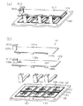
図2は、インバータ装置のカバーを省略した模式斜視図であり、図3は同じく平面図である。図4について(a)は図3のA−A線断面図であり、(b)は(a)の一部省略部分拡大図である。図5は基板上の結線状態を示す部分平面図である。図6について、(a)は図3のB−B線断面図であり、(b)は(a)の部分拡大図である。図7について、(a)はチップ部品が実装されたセラミック基板21の模式斜視図であり、(b)はセラミック基板21が実装された金属ベース20の模式斜視図である。図8について、(a)は金属ベース20に支持枠30が取り付けられた状態の模式斜視図であり、(b)は出力電極部材32U,32V,32Wを取り付けた状態の模式斜視図である。
Next, the structure of the
FIG. 2 is a schematic perspective view in which a cover of the inverter device is omitted, and FIG. 3 is also a plan view. 4A is a cross-sectional view taken along line AA of FIG. 3, and FIG. 4B is an enlarged view of a part of FIG. FIG. 5 is a partial plan view showing a connection state on the substrate. 6A is a cross-sectional view taken along the line BB of FIG. 3, and FIG. 6B is a partially enlarged view of FIG. 7A is a schematic perspective view of the
図2及び図3に示すように、インバータ装置11は、銅製の金属ベース20と、絶縁基板としてのセラミック基板21とで構成された基板22上に半導体チップ23が実装されている。半導体チップ23は、1個のスイッチング素子(MOSFET)及び1個のダイオードが一つのデバイスとして組み込まれている。即ち、半導体チップ23は、図1(b)に示される一つのスイッチング素子Q及び一つのダイオードDを備えたデバイスとなる。
As shown in FIGS. 2 and 3, in the
セラミック基板21は、図5に示すように、表面に回路パターン24a,24b,24c,24dを有し、図4(b)に示すように、裏面にセラミック基板21と金属ベース20とを接合する接合層として機能する金属板25を有するセラミック板26で構成されている。セラミック板26は、例えば、窒化アルミニウム、アルミナ、窒化ケイ素等により形成され、回路パターン24a,24b,24c,24d及び金属板25は、例えば、アルミニウムや銅等で形成されている。セラミック基板21は、金属板25を介して半田(図示せず)で金属ベース20に接合されている。以下、この明細書では、金属ベース20をインバータ装置11の底部(下部)として説明する。
As shown in FIG. 5, the
図5に示すように回路パターン24aはゲート信号用の回路パターン、回路パターン24bはドレイン用の回路パターン、回路パターン24cはソース用の回路パターン、回路パターン24dはソース信号用の回路パターンである。各回路パターン24a,24b,24c,24dは帯状に形成されている。ドレイン用の回路パターン24bと、ソース用の回路パターン24cとは、隣接して平行に延びるように形成され、ゲート信号用の回路パターン24a及びソース信号用の回路パターン24dは、回路パターン24cと反対側において回路パターン24bと平行に延びるように形成されている。半導体チップ23は、ドレイン用の回路パターン24b上に半田で接合されている。半導体チップ23は、ゲートとゲート信号用の回路パターン24aとの間、ソースとソース用の回路パターン24cとの間及びソースとソース信号用の回路パターン24dとの間をワイヤボンディングにより電気的に接続されている。
As shown in FIG. 5, the
図7(b)に示すように、金属ベース20はほぼ矩形状に形成され、セラミック基板21も矩形状に形成されている。セラミック基板21は12個設けられ、長手方向が金属ベース20の長手方向と直交する状態で各列6個となるように2列、6行に配置されている。そして、各行の2個のセラミック基板21上に配置された半導体チップ23がインバータ回路12の各アームを構成する。この実施形態では、半導体チップ23は、各セラミック基板21上に2個ずつ実装されており、4個の半導体チップ23がそれぞれ1つのアームを構成する。図5に示すように半導体チップ23は回路パターン24bの長手方向中央部にスペースが存在し、スペースの両側に半導体チップ23が1個ずつ位置するように配置されている。
As shown in FIG. 7B, the
図3,4に示すように、基板22の上には板状の正極用配線部材27及び負極用配線部材28が配置されている。この実施形態では、正極用配線部材27の上方に負極用配線部材28が配置されている。正極用配線部材27は図1(a)における配線13を、負極用配線部材28は図1(a)における配線15をそれぞれ構成する。
As shown in FIGS. 3 and 4, a plate-like positive
図4において正極用配線部材27及び負極用配線部材28について、長方形の平板状をなす本体部27a,28aは、基板22の上方において基板22と平行に、かつ相互に絶縁された状態で近接して重なるように配置されている。基板側延設部としての垂下部27b,28bが、本体部27a,28aの幅方向の端部両側から屈曲し基板22側に向かって延びている。垂下部27b,28bは、図4(b)等に示すように本体部27a,28aの幅方向の中心線に対して線対称に設けられている。垂下部27b,28bは、互いに重なる状態で配置されている。このように正極用配線部材27及び負極用配線部材28は、本体部27a,28aから基板22に向かって延びる基板側延設部としての垂下部27b,28bが平板状に形成され、かつ、垂下部27b,28bは、基板22(セラミック基板21)との接合部の直近まで平行状態で互いに近接した状態に保持されている。
In FIG. 4, for the positive
垂下部27b,28bの下端から端子部27c,28cが下方に延び、さらに、その下端から本体部27a,28aと平行に延びるように屈曲形成されている(図2参照)。端子部27c,28cは複数(この実施形態では3対6個)設けられている。端子部27cの先端において接合部27c1が、上アームを構成するセラミック基板21上のドレイン用の回路パターン24bの中央部に超音波接合されている。一方、端子部28cの先端において接合部28c1が、下アームを構成するセラミック基板21上のソース用の回路パターン24cの中央部に超音波接合されている。そして、各接合部27c1,28c1は、図3に示すように配線部材27,28の同じ側に配置された各端子部27c,28cの超音波接合箇所が一直線上に位置するように設けられて、各回路パターン24b,24cに超音波接合されている。
The
図6において垂下部27b,28bには切り欠き部27d,28dが複数、それぞれ対向するように設けられている。この切り欠き部27d,28dは垂下部27b,28bの下端から垂下部27b,28bの上端まで延設されている。また、正極用配線部材27及び負極用配線部材28での1つの垂下部27b,28bにつき3つの端子部27c,28cが基板22に接合されており、切り欠き部27d,28dは正極用配線部材27及び負極用配線部材28の垂下部27b,28bにおける端子部27c,28cの間に形成されている。この切り欠き部27d,28dの幅はゲルの通過に支障のない大きさに形成されている。
In FIG. 6, a plurality of
一方、正極用配線部材27の本体部27aと負極用配線部材28の本体部28aとの間には、両者の電気的絶縁性を確保するための絶縁シート29(図4(b)に図示)が配置されている。絶縁シート29として樹脂シートを挙げることができる。また、正極用配線部材27の本体部27a、負極用配線部材28の本体部28a及び絶縁シート29にはコンデンサ17の正極端子17a及び負極端子17bを挿通可能な長孔が形成されている。
On the other hand, between the
図2,3に示すように、金属ベース20には、その周縁に沿うように電気的絶縁性の支持枠30が、全てのセラミック基板21を枠内に収容する状態に固定されている。正極用配線部材27の本体部27aの長手方向の一端部には、外部電源入力用のプラス入力端子14が形成されている。プラス入力端子14は、一部が支持枠30の外側に位置するように配置されている。負極用配線部材28の本体部28aには、その長手方向の正極用配線部材27のプラス入力端子14が形成された側と反対側の端部に、外部電源入力用のマイナス入力端子16が形成されている。マイナス入力端子16も、一部が支持枠30の外側に位置するように配置されている。
As shown in FIGS. 2 and 3, an electrically insulating
図4に示すように、負極用配線部材28の本体部28a上、即ち正極用配線部材27の本体部27a及び負極用配線部材28の本体部28aうちの基板22と対向しない一方の配線部材の本体部上に、複数(この実施形態では4個)のコンデンサ17が正極端子17a及び負極端子17bが下向きになる状態で電気的な絶縁部材(図示せず)を介して配置されている。各コンデンサ17は、正極端子17a及び負極端子17bがコンデンサ本体の一方の側に設けられ、正極端子17aが正極用配線部材27の本体部27aに接続され、負極端子17bが負極用配線部材28の本体部28aに接続されている。
As shown in FIG. 4, on the
図2及び図3等に示すように、インバータ装置11の3つの出力電極部材32U,32V,32Wは、側面ほぼL字状に形成されるとともに、上方に向かって延びる部分が支持枠30の近くに位置し、横方向に延びる部分が正極用配線部材27の本体部27aの下方においてその長手方向と直交する状態で配置されている。正極用配線部材27と出力電極部材32U,32V,32Wとは、シリコーンゲル36(図4(a)に図示)で絶縁が確保されている。また、ゲル36を用いて正極用配線部材27の垂下部27bと負極用配線部材28の垂下部28bとの絶縁が確保されている。出力電極部材32Uは、第1のスイッチング素子Q1及びダイオードD1で構成される上アームのソース用の回路パターン24cと、第2のスイッチング素子Q2及びダイオードD2で構成される下アームのドレイン用の回路パターン24bとに超音波接合されている。出力電極部材32Vは、第3のスイッチング素子Q3及びダイオードD3で構成される上アームのソース用の回路パターン24cと、第4のスイッチング素子Q4及びダイオードD4で構成される下アームのドレイン用の回路パターン24bとに超音波接合されている。出力電極部材32Wは、第5のスイッチング素子Q5及びダイオードD5で構成される上アームのソース用の回路パターン24cと、第6のスイッチング素子Q6及びダイオードD6で構成される下アームのドレイン用の回路パターン24bとに超音波接合されている。
As shown in FIGS. 2 and 3, the three output electrode members 32 </ b> U, 32 </ b> V, and 32 </ b> W of the
図3等に示すように、各出力電極部材32U,32V,32Wは、セラミック基板21とほぼ同じ幅の銅板をプレス加工することで形成されている。図5に示すように、各出力電極部材32U,32V,32Wには、上アームを構成する2個のセラミック基板21の回路パターン24bのほぼ中央部と、下アームを構成する2個のセラミック基板21の回路パターン24cのほぼ中央部にそれぞれ接合される合計4個の接合部35がそれぞれ設けられている。図8(b)に示すように各出力電極部材32U,32V,32Wは、ほぼL字状に屈曲され、かつ2個の接合部35が水平に延びる部分の先端両側で、2個の接合部35が屈曲部寄りでそれぞれ下側に突出するように形成されている。各出力電極部材32U,32V,32Wは、各2個の接合部35の間に負極用配線部材28の端子部28cを配置可能な空間50が設けられている。そして、各2個の接合部35は、図3に示すように、正極用配線部材27及び負極用配線部材28の接合部27c1,28c1と一直線上に位置するように回路パターン24b,24c上に接合されている。
As shown in FIG. 3 etc., each
図3,5に示すように、各アームに対応するそれぞれ2個のセラミック基板21のうち、出力電極部材32U,32V,32Wの先端側と対応するセラミック基板21のゲート信号用の回路パターン24aには、駆動信号入力端子G1〜G6の第1端部が、ソース信号用の回路パターン24dには信号端子S1〜S6の第1端部が、それぞれ接合されている。各端子G1〜G6,S1〜S6は、図3に示すように、第2端部が支持枠30から突出するように、支持枠30を貫通する状態で支持枠30に一体成形されている。なお、図5において各アームを構成する2個のセラミック基板21上に形成された、回路パターン24a同士及び回路パターン24d同士はそれぞれワイヤボンディングで電気的に接続されている。
As shown in FIGS. 3 and 5, the
図4(a)に示すように、支持枠30内には半導体チップ23の絶縁性確保や保護のためにシリコーンゲル36が充填、硬化されている。そして、金属ベース20上には、基板22の半導体チップ23、即ちスイッチング素子Q1〜Q6が実装された側の面、正極用配線部材27、負極用配線部材28、コンデンサ17、出力電極部材32U,32V,32W及び支持枠30を囲繞するカバー37がボルトにより固定されるようになっている。
As shown in FIG. 4A,
次に前記のように構成されたインバータ装置11の製造方法を説明する。
先ずセラミック基板21上への半導体チップ23の実装工程が行われる。この工程では、図7(a)に示すように、セラミック基板21のドレイン用の回路パターン24b上に2個の半導体チップ23を、回路パターン24bの長手方向の中央部にスペースが存在するように半田付けにより接合する。次に図5に示したように半導体チップ23のゲートとゲート信号用の回路パターン24aとの間、半導体チップ23のソースとソース用の回路パターン24cとの間及び半導体チップ23のソースとソース信号用の回路パターン24dとの間をワイヤボンディングにより電気的に接続する。
Next, a method for manufacturing the
First, the mounting process of the
次にセラミック基板21を金属ベース20上に接合する工程が行われる。この工程では、図7(b)に示すように、半導体チップ23が実装されたセラミック基板21を金属ベース20上に、6行2列に半田付けで接合し、図5に示すように同じアームを構成する各2個のセラミック基板21のゲート信号用の回路パターン24a同士及びソース信号用の回路パターン24d同士をワイヤボンディングにより電気的に接続する。
Next, a step of bonding the
次に出力電極部材32U,32V,32Wをセラミック基板21に接合する工程が行われる。この工程では、図8(a)に示すように、先ず駆動信号入力端子G1〜G6及び信号端子S1〜S6が装備された支持枠30を、金属ベース20上にセラミック基板21を囲むように固定する。支持枠30の固定は接着剤やねじを用いて行われる。次に出力電極部材32U,32V,32Wを、図8(b)に示すように、各接合部35がドレイン用の回路パターン24b及びソース用の回路パターン24cのほぼ中央部と当接するように配置する(図5参照)。そして、超音波接合により各接合部35を順次回路パターン24b及び回路パターン24cに接合する。また、駆動信号入力端子G1〜G6の第1端部を回路パターン24aに、信号端子S1〜S6の第1端部を回路パターン24dに、それぞれ超音波接合により接合する。
Next, a step of joining the
次に図9におけるコンデンサアッシー(組立品)38を組み立てる工程が行われる。この工程では、4個のコンデンサ17を正極端子17a及び負極端子17bが上向きになる状態において、所定間隔で1列に治具で固定する。その状態で絶縁材を介して負極用配線部材28を各コンデンサ17の負極端子17bにねじで固定する。次に絶縁シート29を負極用配線部材28の本体部28aとの間に配置した状態で正極用配線部材27をコンデンサ17の正極端子17aにねじで固定する。以上により、正極用配線部材27の本体部27a及び負極用配線部材28の本体部28a間の絶縁が確保された状態で、コンデンサ17の正極端子17aに正極用配線部材27が、負極端子17bに負極用配線部材28がそれぞれ電気的に接合されたコンデンサアッシー38(図9参照)が組み立てられる。
Next, a process of assembling the capacitor assembly (assembly) 38 in FIG. 9 is performed. In this step, the four
次にセラミック基板21にコンデンサアッシー38を超音波接合する工程が行われる。この工程では、先ず、コンデンサアッシー38をセラミック基板21上に載置する。図9に示すように、コンデンサアッシー38は、セラミック基板21の上方から支持枠30内の所定位置に配置される。この状態では、図3に示すように、正極用配線部材27及び負極用配線部材28の幅方向の同じ側に配置された各接合部27c1,28c1が一直線上に位置する状態になる。
Next, a step of ultrasonically bonding the
その状態で各接合部27c1,28c1を順に超音波接合で回路パターン24b,24cに接合する。接合部27c1,28c1とコンデンサ17とが近いため、端子部27c,28cの接合に半田付けを用いる場合、一般の耐熱性を特に考慮していないコンデンサを使用すると、半田付けのための加熱によりコンデンサ17が悪影響を受ける虞がある。しかし、接合部27c1,28c1の接合が超音波接合で行われるため、コンデンサ17に加わる熱量が小さくなり、耐熱性の高い特殊なコンデンサを使用する必要がない。
In this state, the joint portions 27c1 and 28c1 are joined to the
次に図4に示すように半導体チップ23や各接合部等湿気や酸化を嫌う部分の電気的絶縁及び保護のため、支持枠30内へのシリコーンゲル36の注入、硬化処理が行われる(シリコーンゲル36の充填、硬化が行われる)。ここで、図6に示すごとく正極用配線部材27及び負極用配線部材28の垂下部27b,28bに切り欠き部27d,28dが形成されているため、切り欠き部27d,28dがない場合に比較して、シリコーンゲルの注入時にシリコーンゲルが正極用配線部材27と負極用配線部材28との間に容易に流入する。そして、最後に図4(a)に示すようにカバー37が金属ベース20にボルトにより固定されて、インバータ装置11が完成する。
Next, as shown in FIG. 4, in order to electrically insulate and protect the
次に前記のように構成されたインバータ装置11の作用を説明する。
インバータ装置11は、例えば、車両の電源装置の一部を構成するものとして使用される。図1においてインバータ装置11は、プラス入力端子14及びマイナス入力端子16が直流電源(図示せず)に接続され、U相端子U、V相端子V及びW相端子Wがモータ(図示せず)に接続され、駆動信号入力端子G1〜G6及び信号端子S1〜S6が制御装置(図示せず)に接続された状態で使用される。
Next, the operation of the
The
上アームの第1、第3及び第5のスイッチング素子Q1,Q3,Q5及び下アームの第2、第4及び第6のスイッチング素子Q2,Q4,Q6がそれぞれ所定周期でオン、オフ制御されることによりモータに交流が供給されてモータが駆動される。 The first, third, and fifth switching elements Q1, Q3, and Q5 of the upper arm and the second, fourth, and sixth switching elements Q2, Q4, and Q6 of the lower arm are turned on and off at predetermined intervals, respectively. As a result, alternating current is supplied to the motor to drive the motor.
図2等において正極用配線部材27及び負極用配線部材28には、スイッチング素子Q1〜Q6のスイッチング時に急峻に立ち上がる電流又は立ち下がる電流が流れ、その電流は正極用配線部材27及び負極用配線部材28で逆方向となる。正極用配線部材27及び負極用配線部材28の本体部27a,28aは平行な平板状に形成され、互いに近接して配置されているため、相互インダクタンスの効果により配線インダクタンスが低減する。また、垂下部27b,28bも平行に近接して配置されているため、即ち、互いに逆方向に流れる電流に対応する垂下部27b,28bにおいてインダクタンスをより低減することができる。
In FIG. 2 and the like, the
このようにしてコンデンサ17から半導体チップ23の直近までの配線のインダクタンスを低減でき、スイッチング素子Q1〜Q6のスイッチング動作時に発生するサージ電圧を抑制して半導体チップ23の破損を防止することができる。
Thus, the inductance of the wiring from the
また、金属ベース20がヒートシンク(放熱板)として機能する。そして、スイッチング素子Q1〜Q6、ダイオードD1〜D6が通電に伴い発熱し、金属ベース20がその熱により伸縮する。これにより、正極用配線部材27及び負極用配線部材28とセラミック基板21との接合部に応力が加わる。このとき、正極用配線部材27及び負極用配線部材28における垂下部27b,28bが平板状に形成され、かつ、当該平板状の垂下部27b,28bには本体部27a,28aの長手方向と交差する方向に切り欠き部27d,28dが垂下部27b,28bの上端まで形成されている。この切り欠き部27d,28dの存在により接合部に加わる応力が低減される。
Further, the
このように熱サイクルが加わった際において金属ベース20とセラミック基板21の熱膨張係数の差により接合部に応力が加わる以外にも、正極用配線部材27及び負極用配線部材28とセラミック基板21との接合時に熱膨張係数の差により接合部に応力が加わるが、切り欠き部27d,28dの存在により接合部に加わる応力が低減される。
In addition to applying stress to the joint due to the difference in thermal expansion coefficient between the
また、切り欠き部27d,28dが垂下部27b,28bにおける基板22との接合部の間の領域において形成されているので、金属ベース20が熱により伸縮することで、正極用配線部材27及び負極用配線部材28の垂下部27b,28bにおけるセラミック基板21との接合部の間の領域において応力が加わるが、切り欠き部27d,28dにより応力緩和が図られる。また、切り欠き部27d,28dにより電流の流れを規制することもできる。つまり、図1(a),図6(a)における正極用配線部材27を通して上アームに入る電流i1,i2,i3を規制できるとともに負極用配線部材28を通して下アームから出る電流i4,i5,i6を規制できる。
Further, since the
上記実施形態によれば、以下のような効果を得ることができる。
(1)正極用配線部材27及び負極用配線部材28は、本体部27a,28aから基板22に向かって延びる垂下部(基板側延設部)27b,28bが平板状に形成され、かつ、垂下部27b,28bから延びる端子部27c,28cにて基板22に接合されるとともに平板状の垂下部27b,28bには切り欠き部27d,28dが垂下部27b,28bの下端から垂下部27b,28bの上端まで延設されている。よって、基板22が熱により伸縮することで正極用配線部材27及び負極用配線部材28と基板22との接合部に加わる応力を低減することができる。
According to the above embodiment, the following effects can be obtained.
(1) The positive
(2)端子部27c,28cは複数設けられ、複数の端子部27c,28cが基板22に接合され、正極用配線部材27及び負極用配線部材28の垂下部27b,28bにおける端子部27c,28cの間に切り欠き部27d,28dが形成されている。これにより、基板22が熱により伸縮することで、正極用配線部材27及び負極用配線部材28の垂下部27b,28bにおける端子部27c,28cの間に応力が加わるが、端子部27c,28c間(接合部間)に設けた切り欠き部27d,28dによって、より効率的に応力緩和が図られる。
(2) A plurality of
(3)基板22と平行に配置した正極用配線部材の本体部27a及び負極用配線部材の本体部28aのうちの基板22と対向しない一方の本体部28a上にコンデンサ17が搭載されているで、コンデンサ17をスイッチング素子としての半導体チップ23を含めた基板側部品に一体化することができる。
(3) The
実施形態は前記に限定されるものではなく、例えば、次のように具体化してもよい。
○ 配線部材27,28の垂下部(基板側延設部)27b,28bに切り欠き部27d,28dを、垂下部27b,28bの下端から垂下部27b,28bの上端まで延設したが、切り欠き部を、垂下部27b,28bの下端から垂下部27b,28bの上端を超えて延設してもよい。要は、切り欠き部27d,28dは垂下部27b,28bの下端から少なくとも垂下部27b,28bの上端まで延設されていればよい。
The embodiment is not limited to the above, and may be embodied as follows, for example.
○
○ 図4(b)での絶縁シート29に代わり板状のもの(例えば樹脂板)を用いることができ、他にも、正極用配線部材27及び負極用配線部材28の全体をゲルで絶縁してもよい。
○ Instead of the insulating
○ 正極用配線部材27及び負極用配線部材28とセラミック基板21との接合は超音波接合以外にもレーザ溶接や半田付け等でもよい。同様に、出力電極部材32U,32V,32Wとセラミック基板21との接合は超音波接合以外にもレーザ溶接や半田付け等でもよい。さらに、駆動信号入力端子G1〜G6及び信号端子S1〜S6とセラミック基板21との接合は超音波接合以外にもレーザ溶接や半田付け等でもよい。
The joining of the positive
○ 正極用配線部材27及び負極用配線部材28の本体部27a,28aは、基板22と平行に、かつ相互に絶縁された状態で近接して重なるように配置されていればよく、負極用配線部材28が上側、即ち基板22と対向しない側に配置される構成に限らず、正極用配線部材27が上側に配置される構成としてもよい。しかし、電解コンデンサの場合、外側がグランドのため、負極用配線部材28が上側に配置される方が好ましい。
The
○ コンデンサ17の配置は、基板22と対応する位置、即ち金属ベース20の上方に限らない。例えば、図10に示すように、金属ベース20の側方に配置してもよい。正極用配線部材27及び負極用配線部材28は、負極用配線部材28の本体部28aがコンデンサ17側、即ち下側になるように平行に配置されるとともに、垂下部27b,28b,端子部27c,28cが正極用配線部材27の本体部27a及び負極用配線部材28の本体部28aの先端から下方に屈曲形成されている。そして、正極用配線部材27の接合部27c1がセラミック基板21上のドレイン用の回路パターン24bに接合され、負極用配線部材28の接合部28c1がセラミック基板21上のソース用の回路パターン24cに接合されている。この実施形態では、各アームが1個のセラミック基板21上に2個の半導体チップ23が実装された構成で、図10の紙面と垂直方向にセラミック基板21が6列に配置された構成になっている。そして、図10では回路パターン24b以外の回路基板や出力電極部材32U等の図示を省略している。この場合も、平板状の垂下部27b,28bに切り欠き部27d,28dを垂下部27b,28bの下端から少なくとも垂下部27b,28bの上端まで延設することにより、基板22が熱により伸縮することで正極用配線部材27及び負極用配線部材28と基板22との接合部に応力が加わるが、切り欠き部27d,28dの存在により接合部に加わる応力が低減される。また、切り欠き部27d,28dを垂下部27b,28bにおける基板22との接合部の間の領域において形成することにより、基板22が熱により伸縮することで、正極用配線部材27及び負極用配線部材28の垂下部27b,28bにおける基板22との接合部の間の領域において応力が加わるが、切り欠き部27d,28dにより応力緩和が図られる。なお、図10では、セラミック基板21を金属ベース20に接合するための半田H及び半導体チップ23を回路パターン24bに接合するための半田Hを図示している。
The arrangement of the
○ 各アームを2個のセラミック基板21で構成する代わりに、1個のセラミック基板21で構成してもよく、この場合、ゲート信号用の回路パターン24a間及びソース信号用の回路パターン24d間をそれぞれ電気的に接続するワイヤボンディングが不要になる。また、各アームのドレイン用の回路パターン24b及びソース用の回路パターン24cと、正極用配線部材27、負極用配線部材28及び出力電極部材32U,32V,32Wの各接合部27c1,28c1,35との接合箇所は2箇所でなく、1箇所ずつでもよくなる。
Each arm may be composed of one
○ 各アームを構成するセラミック基板21を1個にしてセラミック基板21の数を少なくする構成に限らず、1個のセラミック基板21上に複数のアームを構成するようにしてもよい。
The present invention is not limited to a configuration in which the number of
○ 金属ベース20をアルミニウム系金属で形成し、セラミック基板21として、両面にアルミニウム層が形成されたDBA(Direct Brazing Aluminum )基板を用い、DBA 基板の表面に回路パターン24a,24b,24c,24dを形成し、裏面を金属ベース20にアルミニウム系ろう材によりろう付けしてもよい。
A DBA (Direct Brazing Aluminum) substrate in which the
○ セラミック基板21に代えて、絶縁基板として金属基板の表面に絶縁層を形成し、絶縁層上に回路パターン24a,24b,24c,24dを形成した構成の物を使用してもよい。
O Instead of the
○ 金属ベース20上に絶縁基板を半田付けあるいはろう付けで接合する代わりに、金属ベース20上に絶縁層を形成し、その絶縁層上に回路パターン24a,24b,24c,24dを形成してもよい。この場合、部品点数が少なくなるとともに、絶縁基板を金属ベース20上に接合する工程が不要になる。
○ Instead of joining the insulating substrate on the
○ コンデンサ17の数は4個に限らず、インバータ装置11の定格電流値及び使用するコンデンサの容量により決まり、3個以下でも5個以上でもよい。
○ コンデンサ17は電解コンデンサに限らず、例えば電気二重層コンデンサであってもよい。
The number of
The
○ スイッチング素子Q,Q1〜Q6はMOSFETに限らず、他のパワートランジスタ(例えば、IGBT(絶縁ゲートバイポーラ型トランジスタ))やサイリスタを使用してもよい。 The switching elements Q, Q1 to Q6 are not limited to MOSFETs, and other power transistors (for example, IGBT (insulated gate bipolar transistor)) or thyristors may be used.
○ 各アームを構成するスイッチング素子Q及びダイオードDの組は4組に限らず、各アームを流れる電流量の大きさによって3組以下でも5組以上でもよい。また、複数組に限らず、1組のスイッチング素子Q及びダイオードDの組で構成されてもよい。 The group of switching elements Q and diodes D constituting each arm is not limited to four, and may be three or less or five or more depending on the amount of current flowing through each arm. Moreover, it is not limited to a plurality of sets, and may be configured by a set of a switching element Q and a diode D.
○ 1組のスイッチング素子及びダイオードは、1個の半導体チップ23としてパッケージ化される構成に限らず、スイッチング素子及びダイオードがそれぞれ回路パターン上に実装された構成でもよい。
The pair of switching elements and diodes is not limited to the configuration packaged as one
○ インバータ装置11は、3相交流を出力する構成に限らず、単相交流を出力する構成としてもよい。単相交流を出力する構成では上アーム及び下アームの組が2組存在する。
(Circle) the
○ 電力変換装置は、インバータ装置11に限らず、例えば、DC−DCコンバータに適用してもよい。
○ コンデンサ17の正極端子17aと正極用配線部材27との接合及び負極端子17bと負極用配線部材28との接合は、ねじによる締め付け固定に限らず、コンデンサ17に対する熱の影響が半田付けに比較して小さな接合方法、例えば、精密抵抗溶接やレーザビーム溶接で行ってもよい。
(Circle) not only the
The joining of the
Q,Q1,Q2,Q3,Q4,Q5,Q6…スイッチング素子、11…インバータ装置、17…コンデンサ、17a…正極端子、17b…負極端子、20…金属ベース、21…セラミック基板、22…基板、23…スイッチング素子としての半導体チップ、24b,24c…回路パターン、26…セラミック板、27…正極用配線部材、27a…本体部、27b…基板側延設部としての垂下部、27c…端子部、27c1…接合部、27d…切り欠き部、28…負極用配線部材、28a…本体部、28b…基板側延設部としての垂下部、28c…端子部、28c1…接合部、28d…切り欠き部。 Q, Q1, Q2, Q3, Q4, Q5, Q6 ... switching element, 11 ... inverter device, 17 ... capacitor, 17a ... positive electrode terminal, 17b ... negative electrode terminal, 20 ... metal base, 21 ... ceramic substrate, 22 ... substrate, 23 ... Semiconductor chip as switching element, 24b, 24c ... Circuit pattern, 26 ... Ceramic plate, 27 ... Wiring member for positive electrode, 27a ... Main body part, 27b ... Hanging part as extension part on substrate side, 27c ... Terminal part, 27c1 ... Junction part, 27d ... Notch part, 28 ... Negative electrode wiring member, 28a ... Main body part, 28b ... Draft part as a board side extension part, 28c ... Terminal part, 28c1 ... Joint part, 28d ... Notch part .
Claims (2)
平板状の本体部が前記基板の上方において前記基板と平行に、かつ相互に電気的に絶縁された状態で近接して重なるように配置された正極用配線部材及び負極用配線部材と、
正極端子が前記正極用配線部材の本体部に接続され、負極端子が前記負極用配線部材の本体部に接続されたコンデンサと、
を備え、
前記正極用配線部材及び負極用配線部材は、前記本体部の幅方向の両端部から前記基板に向かって延びる基板側延設部が平板状に形成され、かつ、前記基板側延設部が平行状態で互いに近接した状態とされ、かつ、前記基板側延設部から延びる端子部にて前記基板に接合されるとともに当該近接した状態の各基板側延設部には切り欠き部が両基板側延設部間で互いに対向するように設けられ、当該切り欠き部が基板側延設部の下端から少なくとも基板側延設部の上端まで延設され、
前記基板と平行に配置した前記正極用配線部材の本体部及び負極用配線部材の本体部のうちの前記基板と対向しない一方の本体部上にコンデンサが搭載されていることを特徴とする電力変換装置。 A substrate on which a switching element is mounted;
A positive electrode wiring member and a negative electrode wiring member arranged so that the flat plate-like main body portion is adjacent to and overlaps with the substrate in a state of being electrically insulated from each other above the substrate;
A capacitor in which a positive terminal is connected to the main body of the positive wiring member, and a negative terminal is connected to the main body of the negative wiring member;
With
In the positive electrode wiring member and the negative electrode wiring member, a substrate side extending portion extending from both end portions in the width direction of the main body portion toward the substrate is formed in a flat plate shape, and the substrate side extending portion is parallel. In the state of being close to each other and being joined to the substrate at a terminal portion extending from the substrate-side extension portion, each substrate-side extension portion in the proximity state has a notch on both substrate sides. Provided so as to be opposed to each other between the extended portions, the notch portion is extended from the lower end of the substrate side extended portion to at least the upper end of the substrate side extended portion ,
A power conversion , wherein a capacitor is mounted on one of the main body portion of the positive electrode wiring member and the main body portion of the negative electrode wiring member arranged in parallel to the substrate, the main body portion not facing the substrate. apparatus.
Priority Applications (4)
| Application Number | Priority Date | Filing Date | Title |
|---|---|---|---|
| JP2008054051A JP4640425B2 (en) | 2008-03-04 | 2008-03-04 | Power converter |
| EP09003031.3A EP2099120B1 (en) | 2008-03-04 | 2009-03-03 | Power converter |
| CN200910127005A CN101527303A (en) | 2008-03-04 | 2009-03-03 | Power converter |
| US12/397,215 US8040707B2 (en) | 2008-03-04 | 2009-03-03 | Power converter |
Applications Claiming Priority (1)
| Application Number | Priority Date | Filing Date | Title |
|---|---|---|---|
| JP2008054051A JP4640425B2 (en) | 2008-03-04 | 2008-03-04 | Power converter |
Publications (2)
| Publication Number | Publication Date |
|---|---|
| JP2009213272A JP2009213272A (en) | 2009-09-17 |
| JP4640425B2 true JP4640425B2 (en) | 2011-03-02 |
Family
ID=40765647
Family Applications (1)
| Application Number | Title | Priority Date | Filing Date |
|---|---|---|---|
| JP2008054051A Expired - Fee Related JP4640425B2 (en) | 2008-03-04 | 2008-03-04 | Power converter |
Country Status (4)
| Country | Link |
|---|---|
| US (1) | US8040707B2 (en) |
| EP (1) | EP2099120B1 (en) |
| JP (1) | JP4640425B2 (en) |
| CN (1) | CN101527303A (en) |
Families Citing this family (10)
| Publication number | Priority date | Publication date | Assignee | Title |
|---|---|---|---|---|
| DE102010028927A1 (en) | 2010-05-12 | 2011-11-17 | Zf Friedrichshafen Ag | Power electronics arrangement |
| JP2012089565A (en) * | 2010-10-15 | 2012-05-10 | Honda Motor Co Ltd | Semiconductor device |
| JP5782995B2 (en) * | 2011-10-31 | 2015-09-24 | 富士電機株式会社 | Inverter device |
| JP2014110721A (en) * | 2012-12-04 | 2014-06-12 | Samsung Electronics Co Ltd | Power conversion device |
| JP5655846B2 (en) * | 2012-12-04 | 2015-01-21 | 株式会社デンソー | Power converter |
| CN103208473B (en) * | 2012-12-15 | 2016-01-20 | 南京银茂微电子制造有限公司 | Adopt the power model of laser welding terminal |
| US9985453B2 (en) * | 2016-03-03 | 2018-05-29 | GM Global Technology Operations LLC | Apparatus for discharging a high-voltage bus |
| JP6646819B2 (en) * | 2016-03-25 | 2020-02-14 | パナソニックIpマネジメント株式会社 | Switching power supply |
| JP7309396B2 (en) * | 2019-03-18 | 2023-07-18 | 株式会社東芝 | semiconductor equipment |
| JP6979997B2 (en) * | 2019-12-04 | 2021-12-15 | 三菱電機株式会社 | Power semiconductor devices |
Citations (7)
| Publication number | Priority date | Publication date | Assignee | Title |
|---|---|---|---|---|
| JP2000060126A (en) * | 1998-08-11 | 2000-02-25 | Hitachi Ltd | Main circuit structure for power converter |
| JP2002044964A (en) * | 2000-07-21 | 2002-02-08 | Hitachi Ltd | Semiconductor device, power converter and vehicle |
| JP2004214452A (en) * | 2003-01-06 | 2004-07-29 | Fuji Electric Device Technology Co Ltd | Semiconductor module for power and method for connecting to external electrode |
| JP2005347561A (en) * | 2004-06-03 | 2005-12-15 | Toshiba Corp | Power semiconductor module and power conversion apparatus |
| JP2007143272A (en) * | 2005-11-17 | 2007-06-07 | Hitachi Ltd | Capacitor module, power conversion device, and on-vehicle electric machinery system |
| JP2009213271A (en) * | 2008-03-04 | 2009-09-17 | Toyota Industries Corp | Power conversion device |
| JP2009213270A (en) * | 2008-03-04 | 2009-09-17 | Toyota Industries Corp | Power conversion device |
Family Cites Families (7)
| Publication number | Priority date | Publication date | Assignee | Title |
|---|---|---|---|---|
| JP2809095B2 (en) * | 1994-03-04 | 1998-10-08 | 株式会社デンソー | Inverter device |
| JP3228021B2 (en) * | 1994-09-13 | 2001-11-12 | 富士電機株式会社 | Inverter unit and inverter device |
| JPH1169840A (en) * | 1997-08-22 | 1999-03-09 | Aisin Seiki Co Ltd | Switching assembly |
| CA2255441C (en) * | 1997-12-08 | 2003-08-05 | Hiroki Sekiya | Package for semiconductor power device and method for assembling the same |
| JPH11191605A (en) * | 1997-12-26 | 1999-07-13 | Murata Mfg Co Ltd | Electronic component and its manufacture |
| JP3906440B2 (en) * | 2000-09-06 | 2007-04-18 | 株式会社日立製作所 | Semiconductor power converter |
| US6456515B1 (en) * | 2000-11-27 | 2002-09-24 | Briggs & Stratton Corporation | Three-phase H-bridge assembly and method of assembling the same |
-
2008
- 2008-03-04 JP JP2008054051A patent/JP4640425B2/en not_active Expired - Fee Related
-
2009
- 2009-03-03 EP EP09003031.3A patent/EP2099120B1/en not_active Expired - Fee Related
- 2009-03-03 US US12/397,215 patent/US8040707B2/en not_active Expired - Fee Related
- 2009-03-03 CN CN200910127005A patent/CN101527303A/en active Pending
Patent Citations (7)
| Publication number | Priority date | Publication date | Assignee | Title |
|---|---|---|---|---|
| JP2000060126A (en) * | 1998-08-11 | 2000-02-25 | Hitachi Ltd | Main circuit structure for power converter |
| JP2002044964A (en) * | 2000-07-21 | 2002-02-08 | Hitachi Ltd | Semiconductor device, power converter and vehicle |
| JP2004214452A (en) * | 2003-01-06 | 2004-07-29 | Fuji Electric Device Technology Co Ltd | Semiconductor module for power and method for connecting to external electrode |
| JP2005347561A (en) * | 2004-06-03 | 2005-12-15 | Toshiba Corp | Power semiconductor module and power conversion apparatus |
| JP2007143272A (en) * | 2005-11-17 | 2007-06-07 | Hitachi Ltd | Capacitor module, power conversion device, and on-vehicle electric machinery system |
| JP2009213271A (en) * | 2008-03-04 | 2009-09-17 | Toyota Industries Corp | Power conversion device |
| JP2009213270A (en) * | 2008-03-04 | 2009-09-17 | Toyota Industries Corp | Power conversion device |
Also Published As
| Publication number | Publication date |
|---|---|
| EP2099120A2 (en) | 2009-09-09 |
| US8040707B2 (en) | 2011-10-18 |
| EP2099120B1 (en) | 2018-05-16 |
| JP2009213272A (en) | 2009-09-17 |
| US20090225577A1 (en) | 2009-09-10 |
| CN101527303A (en) | 2009-09-09 |
| EP2099120A3 (en) | 2013-11-06 |
Similar Documents
| Publication | Publication Date | Title |
|---|---|---|
| JP4582161B2 (en) | Power converter | |
| JP4640425B2 (en) | Power converter | |
| JP4561874B2 (en) | Power converter | |
| JP4640423B2 (en) | Power converter | |
| JP6763998B2 (en) | Semiconductor module | |
| EP2099119B1 (en) | Power converter apparatus | |
| JP2009278772A (en) | Inverter module | |
| WO2023065602A1 (en) | Power module and motor controller | |
| JP5056595B2 (en) | Power converter | |
| JP5092892B2 (en) | Semiconductor device | |
| EP2099121B1 (en) | Power converter apparatus | |
| JP5062029B2 (en) | Semiconductor device | |
| JP5092804B2 (en) | Power converter | |
| CN110622307B (en) | Semiconductor module and power conversion device | |
| JP2012089794A (en) | Semiconductor device | |
| JP4640424B2 (en) | Power converter | |
| JP6220265B2 (en) | Semiconductor mounting structure and mounting method thereof | |
| JP2012209598A (en) | Semiconductor device |
Legal Events
| Date | Code | Title | Description |
|---|---|---|---|
| A621 | Written request for application examination |
Free format text: JAPANESE INTERMEDIATE CODE: A621 Effective date: 20100224 |
|
| A131 | Notification of reasons for refusal |
Free format text: JAPANESE INTERMEDIATE CODE: A131 Effective date: 20100803 |
|
| A521 | Request for written amendment filed |
Free format text: JAPANESE INTERMEDIATE CODE: A523 Effective date: 20101004 |
|
| TRDD | Decision of grant or rejection written | ||
| A01 | Written decision to grant a patent or to grant a registration (utility model) |
Free format text: JAPANESE INTERMEDIATE CODE: A01 Effective date: 20101102 |
|
| A01 | Written decision to grant a patent or to grant a registration (utility model) |
Free format text: JAPANESE INTERMEDIATE CODE: A01 |
|
| A61 | First payment of annual fees (during grant procedure) |
Free format text: JAPANESE INTERMEDIATE CODE: A61 Effective date: 20101115 |
|
| R151 | Written notification of patent or utility model registration |
Ref document number: 4640425 Country of ref document: JP Free format text: JAPANESE INTERMEDIATE CODE: R151 |
|
| FPAY | Renewal fee payment (event date is renewal date of database) |
Free format text: PAYMENT UNTIL: 20131210 Year of fee payment: 3 |
|
| LAPS | Cancellation because of no payment of annual fees |