JP4637473B2 - Stacked photoelectric conversion device - Google Patents
Stacked photoelectric conversion device Download PDFInfo
- Publication number
- JP4637473B2 JP4637473B2 JP2003398188A JP2003398188A JP4637473B2 JP 4637473 B2 JP4637473 B2 JP 4637473B2 JP 2003398188 A JP2003398188 A JP 2003398188A JP 2003398188 A JP2003398188 A JP 2003398188A JP 4637473 B2 JP4637473 B2 JP 4637473B2
- Authority
- JP
- Japan
- Prior art keywords
- photoelectric conversion
- dye
- light
- film
- conversion device
- Prior art date
- Legal status (The legal status is an assumption and is not a legal conclusion. Google has not performed a legal analysis and makes no representation as to the accuracy of the status listed.)
- Expired - Fee Related
Links
Images


Classifications
-
- Y—GENERAL TAGGING OF NEW TECHNOLOGICAL DEVELOPMENTS; GENERAL TAGGING OF CROSS-SECTIONAL TECHNOLOGIES SPANNING OVER SEVERAL SECTIONS OF THE IPC; TECHNICAL SUBJECTS COVERED BY FORMER USPC CROSS-REFERENCE ART COLLECTIONS [XRACs] AND DIGESTS
- Y02—TECHNOLOGIES OR APPLICATIONS FOR MITIGATION OR ADAPTATION AGAINST CLIMATE CHANGE
- Y02E—REDUCTION OF GREENHOUSE GAS [GHG] EMISSIONS, RELATED TO ENERGY GENERATION, TRANSMISSION OR DISTRIBUTION
- Y02E10/00—Energy generation through renewable energy sources
- Y02E10/50—Photovoltaic [PV] energy
- Y02E10/542—Dye sensitized solar cells
Description
本発明は、高い光電変換効率が期待でき、耐候性に優れ、しかも低コスト化が図れる積層型光電変換装置に関する。 The present invention relates to a stacked photoelectric conversion device that can be expected to have high photoelectric conversion efficiency, is excellent in weather resistance, and can be reduced in cost.
バルク型結晶系シリコン太陽電池は、耐候性に優れ20年以上の耐久性を有することから急速に市場を拡大している。このバルク型結晶系シリコン太陽電池は、高純度の単一材料から成る厚いシリコン半導体基板(約300μm)にpn半導体接合を形成し光電変換を行
なっている。太陽光や可視光は広い波長スペクトルからなるが、半導体のバンドギャップによって光エネルギーの吸収と発電には波長制限があり、単一材料からなる光電変換装置では光電変換効率に限界が生じる。また、厚いシリコン基板は高い材料コストとなる。このため、太陽電池の一般家庭への普及には現在の半額以下の生産コストが切望されている。
Bulk-type crystalline silicon solar cells are rapidly expanding the market due to their excellent weather resistance and durability of more than 20 years. In this bulk-type crystalline silicon solar cell, a pn semiconductor junction is formed on a thick silicon semiconductor substrate (about 300 μm) made of a high-purity single material to perform photoelectric conversion. Although sunlight and visible light have a wide wavelength spectrum, there is a wavelength limitation on light energy absorption and power generation due to the band gap of the semiconductor, and a photoelectric conversion device made of a single material has a limit in photoelectric conversion efficiency. In addition, a thick silicon substrate has a high material cost. For this reason, the production cost of less than half the current cost is eagerly desired for the spread of solar cells to ordinary households.
また、薄膜アモルファスシリコン系太陽電池は、薄いシリコン膜(約0.3μm)で済み
低コストで生産が可能である。また、光劣化の問題についても解消されつつある。しかし、変換効率が低いために市場拡大に至っていない。
In addition, a thin-film amorphous silicon solar cell can be produced at a low cost by using a thin silicon film (about 0.3 μm). Moreover, the problem of light degradation is being solved. However, the market has not expanded due to low conversion efficiency.
また、アモルファスシリコン系光電変換装置と微結晶シリコン系光電変換装置とを薄膜で積層した構成の積層型薄膜シリコン系太陽電池が知られている。同じシリコンでもアモルファスと微結晶では異なるバンドギャップを持つので、これら2つの光電変換装置を積層することで、より広く太陽光スペクトルをカバーして変換効率を上げたもので、積極的な開発とともに量産され始めている。この積層型薄膜シリコン系太陽電池では、アモルファスシリコン光電変換装置の膜厚は0.2μm程度で薄いが、微結晶シリコン光電変換装置
の膜厚は2μm程度で厚い。従って、微結晶シリコン光電変換装置の製造コストが薄膜アモルファスシリコン系太陽電池よりはるかに高いので、急速な市場拡大に至っていない。
In addition, a stacked thin film silicon solar cell having a structure in which an amorphous silicon photoelectric conversion device and a microcrystalline silicon photoelectric conversion device are stacked in a thin film is known. Even with the same silicon, amorphous and microcrystals have different band gaps, so by stacking these two photoelectric conversion devices, the conversion efficiency has been increased by covering the solar spectrum more widely. Being started. In this stacked thin-film silicon solar cell, the amorphous silicon photoelectric conversion device is as thin as about 0.2 μm, but the microcrystalline silicon photoelectric conversion device is as thick as about 2 μm. Therefore, since the manufacturing cost of the microcrystalline silicon photoelectric conversion device is much higher than that of the thin film amorphous silicon solar cell, the market has not been rapidly expanded.
また、色素増感型太陽電池は、高温処理や真空装置を必要としないことから低コスト化に有利であると考えられ、近年急速に研究開発が進められている。この色素増感型太陽電池は、導電性ガラス基板上に構築した粒径数10nmの微粒子を焼結して得られる多孔質の酸化チタン層の粒子表面に、有機色素を単分子吸着させた電極を光作用極として用い、白金をスパッタした導電性ガラス対極との間に、ヨウ素/ヨウ化物レドックス対を含む電解質溶液を満たし、この電解質溶液を封止した構造である。このような多孔質化により、光作用極の表面積を1000倍以上に高めて、吸着色素による光吸収を効率よく行っており、研究レベルで最大10%程度、再現レベルでは7%前後の光電変換効率が知られている。このため、市場投入には更なる光電変換効率の向上が必要とされている。 In addition, since dye-sensitized solar cells do not require high-temperature treatment or vacuum equipment, they are considered to be advantageous for cost reduction, and research and development have been promoted rapidly in recent years. This dye-sensitized solar cell is an electrode in which a single molecule of an organic dye is adsorbed on the particle surface of a porous titanium oxide layer obtained by sintering fine particles having a particle size of several tens of nanometers built on a conductive glass substrate. Is used as a light working electrode, and an electrolyte solution containing an iodine / iodide redox pair is filled between a conductive glass counter electrode sputtered with platinum, and this electrolyte solution is sealed. By making such a porous structure, the surface area of the photoactive electrode is increased more than 1000 times, and light absorption by the adsorbing dye is efficiently performed. Photoelectric conversion of about 10% at the research level and around 7% at the reproduction level. Efficiency is known. For this reason, further improvement in photoelectric conversion efficiency is required for market introduction.
色素増感型太陽電池の変換効率を向上させる方法として、多孔質の酸化物半導体の導電性を向上させる方法や色素の増感能力を高める方法(分光感度の長波長化や波長の広幅化など)が研究されている。このなかで酸化物半導体の導電性を向上させる方法として、酸化物半導体の形状を針状やナノチューブとしたり、粒状であれば焼結を強固にしたり、酸化物半導体の物性をより導電性としたりする研究がなされている。また、色素増感型太陽電池では色素を二酸化チタンなどに担持しているため、紫外線や短波長光によって色素の光劣化が生じることが懸念されている。このため、まず室内用途であるパソコンや携帯電話などの電源として実用化することが検討されている。強い照度の太陽光下では、光入射側に紫外線吸収フィルムなどを挿入して、色素の光劣化を抑制することが考えられているが、この手法で光劣化が完全に抑制されるかどうかは未だ疑問であり、紫外線吸収フィルムなどの挿入は可視光の吸収も生じてしまい光電変換効率の低下を生じる。 Methods for improving the conversion efficiency of dye-sensitized solar cells include improving the conductivity of porous oxide semiconductors and increasing the sensitizing ability of dyes (such as increasing the spectral sensitivity and increasing the wavelength) ) Has been studied. Among these, as a method for improving the conductivity of the oxide semiconductor, the shape of the oxide semiconductor is made into a needle shape or a nanotube. Research has been done. Moreover, since the dye-sensitized solar cell carries the dye on titanium dioxide or the like, there is a concern that the dye may be photodegraded by ultraviolet rays or short wavelength light. For this reason, it is considered to put it into practical use as a power source for personal computers and mobile phones for indoor use. Under strong sunlight, it is considered to insert a UV absorbing film on the light incident side to suppress the photodegradation of the dye. It is still a question, and insertion of an ultraviolet absorbing film or the like causes absorption of visible light, resulting in a decrease in photoelectric conversion efficiency.
ここで、色素増感型太陽電池の光電変換効率を向上させたとする複合型太陽電池の従来例について説明する。特許文献1に開示された複合型太陽電池によれば、太陽光に面した側に色素増感型太陽電池を配し、この色素増感型太陽電池の後側に結晶系シリコン太陽電池を配して、複合型太陽電池を形成している。ルテニウム錯体を用いた色素増感型太陽電池では、波長600nm以下の太陽光を有効に利用することができるとしている。色素には
、ルテニウム錯体のほか、キサンテン系色素を用いることができるとしている。そして、波長600nm以上の太陽光で発電する太陽電池として、単結晶シリコン及び多結晶シリコ
ンを用いた結晶系シリコン太陽電池に注目し、これがシリコンのpn接合によってバンドの勾配が形成され、太陽光のうち波長400nm〜1100nmの光により生成した電子と正孔
が内部電界によって分離され、起電力が発生するとしている。すなわち、この従来例の複合型太陽電池では、太陽光に面した側に、ルテニウム錯体を用いた色素増感型太陽電池を配して、波長300nm〜600nmの光で発電を行い、一方、該色素増感型太陽電池の後側に結晶系シリコン太陽電池を配して、前記色素増感型太陽電池を透過した光のうち波長400
nm〜1100nmで発電を行なうように構成されている。
The power generation is performed at nm to 1100 nm.
バルク型結晶系シリコン太陽電池は、シリコンの厚みが約300μmもあって資源の問題
と材料コストの問題を抱えている。また結晶化に1000℃以上の高温処理が必要でありプロセスコストがかかる。また、発電セルである基板サイズ(約15cm角)に限界があるので、発電セルからモジュール化(メートルサイズ)に要するアセンブルコストがかかる。
Bulk type crystalline silicon solar cells have a problem of resources and material cost because the silicon thickness is about 300 μm. In addition, a high temperature treatment of 1000 ° C. or higher is required for crystallization, and the process cost is high. In addition, since there is a limit to the substrate size (approximately 15 cm square) that is a power generation cell, the assembly cost required for modularization (meter size) from the power generation cell is increased.
薄膜アモルファスシリコン系太陽電池は、薄いシリコン膜厚(約0.3μm)と低温プロ
セス(約300℃)、そして自由サイズの大きな基板を供することにより、前記問題がほと
んど解消できる。しかしながら、アモルファスシリコンはバンドギャップが大きいため、約700nm以下の短波長光しか吸収できないので、光電変換効率が低いという問題を抱え
ている。
The thin film amorphous silicon solar cell can solve almost all of the above problems by providing a thin silicon film (about 0.3 μm), a low temperature process (about 300 ° C.), and a substrate having a large free size. However, since amorphous silicon has a large band gap, it can absorb only short-wavelength light of about 700 nm or less, and thus has a problem of low photoelectric conversion efficiency.
積層型薄膜シリコン系太陽電池は、変換効率を高めるためにアモルファスシリコン系光電変換装置と微結晶シリコン系光電変換装置を積層した構成であり、いずれも薄膜であり低コスト化太陽電池の候補と考えられている。しかしながら、実際には微結晶シリコン光電変換装置の膜厚がアモルファスシリコン光電変換装置の膜厚に対し約10倍であり、これらの製造装置はほぼ同じ高価な大型真空設備(PCVDなど)を用いており、アモルファスシリコン光電変換装置に比べ微結晶シリコン光電変換装置の製造コストが膜厚に比例する傾向があるので、低コスト化できないという問題を抱えている。 Laminated thin-film silicon solar cells have a structure in which amorphous silicon photoelectric conversion devices and microcrystalline silicon photoelectric conversion devices are stacked in order to increase conversion efficiency. It has been. However, in actuality, the film thickness of the microcrystalline silicon photoelectric conversion device is about 10 times that of the amorphous silicon photoelectric conversion device, and these manufacturing apparatuses use almost the same expensive large-scale vacuum equipment (such as PCVD). In addition, since the manufacturing cost of the microcrystalline silicon photoelectric conversion device tends to be proportional to the film thickness as compared with the amorphous silicon photoelectric conversion device, there is a problem that the cost cannot be reduced.
色素増感型太陽電池は、高温処理や真空装置を必要としないことから最も低コストで製造が可能な太陽電池と考えられている。しかしながら、変換効率が低く、バルク型結晶系シリコン太陽電池や積層型薄膜シリコン系太陽電池に及ばない。また色素増感型太陽電池では紫外線や短波長光によって色素の光劣化が生じることが懸念されている。また、太陽光の熱によって色素の光劣化は加速される。現在、最初に室内用途での実用化が検討されているが、これでは真の太陽電池といえない。紫外線吸収フィルムなどの挿入は可視光の吸収も生じ光電変換効率の低下となるので積極的には使えない。こうして色素増感型太陽電池は色素の光劣化や熱劣化の不安がまだ解消されておらず、耐候性に問題がある。 The dye-sensitized solar cell is considered to be a solar cell that can be manufactured at the lowest cost because it does not require a high-temperature treatment or a vacuum apparatus. However, the conversion efficiency is low and it does not reach the bulk type crystalline silicon solar cell and the laminated thin film silicon solar cell. In addition, in dye-sensitized solar cells, there is a concern that photodegradation of the dye may occur due to ultraviolet light or short wavelength light. Moreover, the photodegradation of the pigment is accelerated by the heat of sunlight. At present, practical application for indoor use is first considered, but this is not a true solar cell. Insertion of an ultraviolet absorbing film or the like also absorbs visible light and lowers the photoelectric conversion efficiency, so it cannot be used actively. In this way, the dye-sensitized solar cell has a problem in weather resistance since the fears of light deterioration and heat deterioration of the dye have not yet been solved.
色素増感型太陽電池の光電変換効率を向上させたとする複合型太陽電池の従来例では、太陽光に面した側に色素増感型太陽電池を配し、該色素増感型太陽電池の後側に結晶系シリコン太陽電池とを配して、複合型太陽電池を形成している。この複合太陽電池では、色素増感型太陽電池を太陽光に面した側に配しており、前記のように色素の光劣化や熱劣化の不安がまだ解消されておらず、耐候性の問題を抱えたままである。さらには、光入射側の後側には前記のようなバルク型結晶系シリコン太陽電池を配して高い光電変換効率を得ようとしている。しかしながら、上述したように、バルク型結晶系シリコン太陽電池はシリコンの厚みが約300μmもあって資源の問題と材料コストの問題を抱えている。また、
結晶化に1000℃以上の高温処理が必要でありプロセスコストがかかる。また発電セルである基板サイズに限界があって発電セルからモジュール化に要するアセンブルコストがかかる。
In the conventional example of the composite type solar cell in which the photoelectric conversion efficiency of the dye-sensitized solar cell is improved, the dye-sensitized solar cell is arranged on the side facing the sunlight, and the dye-sensitized solar cell is disposed after the dye-sensitized solar cell. A crystalline silicon solar cell is arranged on the side to form a composite solar cell. In this composite solar cell, the dye-sensitized solar cell is arranged on the side facing the sunlight, and as described above, the fear of light deterioration and heat deterioration of the dye has not been solved yet, and the problem of weather resistance Is still held. Furthermore, a bulk type crystalline silicon solar cell as described above is arranged behind the light incident side to obtain high photoelectric conversion efficiency. However, as described above, the bulk-type crystalline silicon solar cell has a problem of resources and material cost because the thickness of silicon is about 300 μm. Also,
Crystallization requires a high-temperature treatment of 1000 ° C. or higher, and the process cost is high. In addition, there is a limit to the size of the substrate that is the power generation cell, and the assembly cost required for modularization from the power generation cell is increased.
本発明は斯かる事情に鑑みてなされ、変換効率を高めるとともに、低コスト化が可能で、しかも耐候性(光劣化や熱劣化)の問題を大幅に軽減し解消する優れた積層型光電変換装置を提供することを目的とするものである。 The present invention has been made in view of such circumstances, and has an excellent stacked photoelectric conversion device that can improve conversion efficiency, reduce costs, and greatly reduce and eliminate the problem of weather resistance (light deterioration and heat deterioration). Is intended to provide.
上記目的を達成するために、本発明の積層型光電変換装置は、1)一方主面側から光を入射させる透光性基板の他方主面上に、前記透光性基板側から、第1の透明導電層と、非
単結晶光電変換層と、第2の透明導電層と、触媒層と、正孔輸送体と、色素と、電子輸送体とが、この順で配置されていることを特徴とする。
In order to achieve the above object, the stacked photoelectric conversion device according to the present invention includes: 1) the first main surface of the translucent substrate on which light is incident from the first main surface side; The transparent conductive layer, the non-single crystal photoelectric conversion layer, the second transparent conductive layer, the catalyst layer, the hole transporter, the dye, and the electron transporter are arranged in this order. Features.
また、2)上記1)において、前記色素の分光感度のピーク波長が前記非単結晶光電変換層の分光感度のピーク波長より長波長側にあることを特徴とする。 2) In the above 1), the peak wavelength of the spectral sensitivity of the dye is longer than the peak wavelength of the spectral sensitivity of the non-single-crystal photoelectric conversion layer.
さらに、3)上記1)において、前記非単結晶光電変換層はi型の非晶質シリコン層を備えたpin構造を有していることを特徴とする。 3) In the above 1), the non-single-crystal photoelectric conversion layer has a pin structure including an i-type amorphous silicon layer.
本発明の積層型光電変換装置は、第1の透明導電層、非単結晶光電変換層、第2の透明導電層および触媒層を有する薄膜光電変換体と、この薄膜光電変換体を透過した光を吸収する色素を有し該色素の増感作用により光電変換を行なう色素増感型光電変換体とが、この順で積層されているので、薄膜光電変換体で短波長光がよく光電変換され、色素増感型光電変換体で長波長光(透過してしまった短波長光も含む)がよく光電変換され、両光電変換体の変換効率を合わせた変換効率が得られる。 The stacked photoelectric conversion device of the present invention includes a thin film photoelectric converter having a first transparent conductive layer, a non-single-crystal photoelectric conversion layer, a second transparent conductive layer, and a catalyst layer, and light transmitted through the thin film photoelectric converter. Since a dye-sensitized photoelectric converter that has a dye that absorbs light and performs photoelectric conversion by the sensitizing action of the dye is laminated in this order, short-wavelength light is often photoelectrically converted by the thin-film photoelectric converter. In the dye-sensitized photoelectric conversion body, long wavelength light (including transmitted short wavelength light) is often photoelectrically converted, and conversion efficiency combining the conversion efficiency of both photoelectric conversion bodies is obtained.
また、薄膜光電変換体も色素増感型光電変換体もそれぞれが低温プロセスで作製できるので、積層構成をとっても従来の太陽電池より簡便容易にかつ低コストで製造可能である。さらに、光の入射側に薄膜光電変換体を配し、その後側に色素増感型光電変換体を配したことにより、後側の色素増感型光電変換体が太陽光などの強い光を直接受けることがない。しかも、光入射側の薄膜光電変換体ではよりよく短波長光を吸収し長波長光をほとんど透過する。よって、後側に配置された色素増感型光電変換体は、太陽光などの強い光を直接受けることがなく、紫外線が無く短波長光が激減するので色素の光劣化が大幅に軽減し解消できる。また強い光を直接受けることがなく、背面側より容易に色素増感型光電変換体を冷却することにより温度上昇が抑制できて、色素の熱劣化を抑制できる。 In addition, since each of the thin-film photoelectric conversion body and the dye-sensitized photoelectric conversion body can be produced by a low-temperature process, it can be easily and easily manufactured at a lower cost than a conventional solar cell even if it has a laminated structure. Furthermore, a thin-film photoelectric converter is arranged on the light incident side, and a dye-sensitized photoelectric converter is arranged on the rear side, so that the rear dye-sensitized photoelectric converter directly emits strong light such as sunlight. I will not receive it. Moreover, the thin film photoelectric conversion body on the light incident side better absorbs short wavelength light and almost transmits long wavelength light. Therefore, the dye-sensitized photoelectric converter placed on the rear side does not directly receive strong light such as sunlight, and since there is no ultraviolet light and the short wavelength light is drastically reduced, the light deterioration of the dye is greatly reduced and eliminated. it can. In addition, strong light is not directly received, and the temperature increase can be suppressed by cooling the dye-sensitized photoelectric conversion body easily from the back side, and thermal deterioration of the dye can be suppressed.
また、本発明の積層型光電変換装置は、色素の分光感度のピーク波長が薄膜光電変換体の半導体層の分光感度のピーク波長より長波長側にあることにより、それぞれ異なった波長域の光を光電変換できて、高い光電変換効率が得られる。 In addition, the stacked photoelectric conversion device of the present invention is capable of emitting light in different wavelength ranges because the peak wavelength of the spectral sensitivity of the dye is longer than the spectral sensitivity peak wavelength of the semiconductor layer of the thin film photoelectric converter. Photoelectric conversion is possible, and high photoelectric conversion efficiency is obtained.
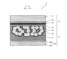
以下、本発明に係る実施形態について図面を参照にしつつ詳細に説明する。本発明の積層型光電変換装置の断面模式図を図1に示す。また、参考としての積層型光電変換装置の断面模式図を図2に示す。図中の矢印は光の入射側を示す。また、図1と図2の相違は、多孔質の一導電型輸送体15とこの多孔質を埋めるように形成した逆多孔質で逆導電型輸送体17との構成が光入射方向に対して反対向きになっている点である。
Hereinafter, embodiments according to the present invention will be described in detail with reference to the drawings. A schematic cross-sectional view of the stacked photoelectric conversion device of the present invention is shown in FIG . FIG . 2 is a schematic cross-sectional view of a stacked photoelectric conversion device as a reference . The arrow in the figure indicates the light incident side. Also, the difference between FIG. 1 and FIG. 2 is that the configuration of the porous one-conducting
図1、図2に示す一実施形態によれば、一方主面側から光を入射させる透光性基板の他方主面上に、薄膜形成法により作製し、光電変換を行なう非単結晶の半導体層を有する薄膜光電変換体である非単結晶光電変換装置2、この非単結晶光電変換装置より長波長側にピーク感度を有し、非単結晶光電変換装置2を透過した光を吸収する色素の増感作用により光電変換を行なう色素増感型光電変換体である色素増感型光電変換装置3を積層して成る。
According to one embodiment shown in FIGS. 1 and 2, a non-single-crystal semiconductor that is produced by thin film formation and photoelectric conversion is performed on the other main surface of a light-transmitting substrate on which light is incident from one main surface side. Non-single crystal
非単結晶光電変換装置2は透光性基板11上に順次形成された第1の透明導電層12、非単結晶光電変換層13、第2の透明導電層14から成る。この非単結晶光電変換層13としては、シリコン系の非単結晶の薄膜pin接合層でもよく、CIGS(CuInGaSe)などの化合物半導体系の薄膜接合層でもよい。また、これらの接合層はpin接合型、pn接合型、ショットキー接合型、ヘテロ接合型など内部電界を生じるものがよい。シリコン系
の非単結晶としては、アモルファスシリコン系、ナノサイズ結晶を含むアモルファスシリコン系、微結晶シリコン系などがよく、特に短波長感度を有するアモルファスシリコン系や光劣化が抑制されるナノサイズ結晶を含むアモルファスシリコン系がよい。ここでアモルファスシリコン系とはアモルファスシリコンカーバイト、アモルファスシリコンナイトライドなどの合金系を含む。
The non-single-crystal
色素増感型光電変換装置3は第2の透明導電層14上に形成されており、多孔質の電子輸送体15、該多孔質を埋めるように形成した逆多孔質の正孔輸送体17、導電性シート18から成るともに、該両輸送体の界面に色素16を配した構成から成る。
The dye-sensitized
非単結晶光電変換層2からの第1の出力と、色素増感型光電変換装置3からの第2の出
力とは、それぞれ独立して出力しても、接続して出力してもよい。本発明のように、積層型光電変換装置の場合、第1の出力の電流と第2の出力の電流とが同じになるように両光
電変換装置の性能を合わせてやれば、第2の透明電極層から外部に出力を取り出す必要がなく集積化などの電極配線構造がシンプルになって具合がよい。両光電流を合わせるにはそれぞれの膜厚や感度などを調整すればよい。
The first output from the non-single crystal
図3に、図2における非単結晶光電変換層2をより詳しく示した参考としての積層型光電変換装置の断面模式図を示す。図3に示す構造は、光が入射される透光性基板11上に、順次、第1の透明導電層12、一導電型シリコン系半導体層13a、実質的に真性である非晶
質シリコン系半導体層13b、逆導電型シリコン系半導体層13c、第2の透明導電層14、多孔質の電子輸送体15、この多孔質を埋めるように形成した逆多孔質の正孔輸送体17、導電性シート18を積層して成るとともに、該両輸送体の界面に(該非晶質シリコン系半導体より長波長側にピーク感度を有する)色素16を配して成る。
FIG. 3 is a schematic cross-sectional view of a stacked photoelectric conversion device as a reference showing the non-single crystal
<透光性基板>
透光性基板11として、鉄成分の少ない白板ガラスが高い透過率で機械的強度もあり最もよい。他に、青板ガラス、硼珪酸ガラス、ソーダガラス、セラミック、サファイアなどの透明無機質基板、ポリカーボネートなどの透明有機樹脂基板などでもよい。また透光性基板11は両面が平坦なものでよいが入射光の波長オーダーの凹凸を有する表面の方が光閉じ込め効果があってなおよい。透光性基板の厚みは材料や基板サイズや用途によるが0.05mm〜6mmがよく、ガラスでメートルサイズの屋根置き用途であれば強度や重量の関係から3mm〜4mmが望ましい。
<Translucent substrate>
As the light-transmitting
<第1の透明導電層> 第1の透明導電層12として、熱CVD法やスプレー熱分解法で作製したフッ素ドープの二酸化スズ膜(SnO2:F膜)が低コストでシート抵抗も小さく最もよい。他に、スパッタ法で作製したスズドープ酸化インジウム膜(ITO膜)、溶液成長法で作製した不純物ドープの酸化亜鉛膜(ZnO膜)、などを用いてもよく、これらを積層して用いてもよい。これらの膜成長によって入射光の波長オーダーの表面凹凸を形成すると光閉じ込め効果があってなおよい。他に、不純物ドープの酸化インジウム膜(In2O3膜)などが使用可能である。また、ディップコート法、ゾル・ゲル法、真空蒸着法、イオンプレーティング法、等で形成できる。
<First Transparent Conductive Layer> As the first transparent
<非単結晶光電変換層>
非単結晶光電変換層13として、プラズマCVD法によって連続堆積したpin接合の水素化アモルファスシリコン系半導体膜がよい。ここで、一導電型シリコン系半導体層13aと逆導電型シリコン系半導体層13cとはそれぞれp型半導体とn型半導体もしくはn型半導体とp型半導体を意味する。また実質的に真性である非晶質シリコン系半導体層13bはi型半導体を意味する。
<Non-single crystal photoelectric conversion layer>
As the non-single-crystal
ここで、i型半導体膜が非晶質であれば、p型半導体膜とn型半導体膜は少なくともいずれかが微結晶でも構わない。また水素化アモルファスシリコン合金系の膜でも構わない。例えば、光入射側のp膜は水素化アモルファスシリコンカーバイドが透光性を高めて光の侵入ロスが少なくより好ましい。他の堆積法として触媒CVD法などで堆積してもよい。プラズマCVD法と触媒CVD法を組み合わせると光劣化が抑制できて信頼性が高まる。これらのシリコン系半導体層13a,13b,13cは、化学気相成長法によりそれぞれの製膜条件で連続堆積できるので具合がよい。
Here, as long as the i-type semiconductor film is amorphous, at least one of the p-type semiconductor film and the n-type semiconductor film may be microcrystalline. Also, a hydrogenated amorphous silicon alloy film may be used. For example, hydrogenated amorphous silicon carbide is more preferable for the p-film on the light incident side because it increases translucency and reduces light penetration loss. Other deposition methods such as catalytic CVD may be used. When plasma CVD and catalytic CVD are combined, photodegradation can be suppressed and reliability can be improved. These silicon-based
より詳しく説明すると、例えば、p型a−Si:H膜の場合、原料ガスとしてSiH4、H2ガス、B2H6(H2で500ppmに希釈したもの)を用い、これらのガスの流量
をそれぞれ最適化し、膜厚は50Å〜200Åの範囲がよく、好適には80Å〜120Åがよく、薄いと内部電界が形成できず厚いと光量損失が増える。続いてi型a−Si:Hの原料ガスとしてSiH4、H2ガスを用い、これらのガスの流量を最適化し、膜厚は500Å〜5000
Å(0.05μm〜0.5μm)の範囲がよく、好適には1500Å〜2500Å(0.15μm〜0.25μm
)、なぜなら薄いと充分な光電流が得られず、厚いと後の色素増感型光電変換装置に光を透過できないからである。続いてn型a−Si:H膜の場合、原料ガスとしてSiH4、H2ガス、PH3(H2で1000ppmに希釈したもの)を用い、これらのガスの流量をそれぞれ最適化し、膜厚は50Å〜200Åの範囲がよく、好適には80Å〜120Åがよく、薄いと内部電界が形成できず厚いと光量損失が増える。基板温度は、pin膜の何れも150℃〜300℃の範囲がよく、好適には180℃〜240℃がよく、低くても高くてもよい光半導体が得られない。
More specifically, for example, in the case of a p-type a-Si: H film, SiH 4 , H 2 gas, and B 2 H 6 (diluted to 500 ppm with H 2 ) are used as source gases, and the flow rates of these gases The film thickness is in the range of 50 mm to 200 mm, preferably 80 mm to 120 mm. If it is thin, an internal electric field cannot be formed, and if it is thick, the light loss increases. Subsequently, SiH 4 and H 2 gases are used as the i-type a-Si: H source gas, the flow rates of these gases are optimized, and the film thickness is 500 to 5000 mm.
The range of Å (0.05 μm to 0.5 μm) is good, preferably 1500 Å to 2500 Å (0.15 μm to 0.25 μm)
) Because, if it is thin, sufficient photocurrent cannot be obtained, and if it is thick, light cannot be transmitted to the subsequent dye-sensitized photoelectric conversion device. Subsequently, in the case of an n-type a-Si: H film, SiH 4 , H 2 gas, and PH 3 (diluted to 1000 ppm with H 2 ) are used as source gases, and the flow rates of these gases are optimized, respectively. Is preferably in the range of 50 mm to 200 mm, preferably 80 mm to 120 mm. If it is thin, an internal electric field cannot be formed, and if it is thick, light loss increases. The substrate temperature is in the range of 150 ° C. to 300 ° C. for any pin film, preferably 180 ° C. to 240 ° C., and an optical semiconductor that may be low or high cannot be obtained.
<第2の透明導電層>
第2の透明導電層14として、低温成長のスパッタ法や低温スプレー熱分解法で作製したスズドープ酸化インジウム膜(ITO膜)がよい。他に、溶液成長法で作製した不純物ドープの酸化亜鉛膜(ZnO膜)、熱CVD法で形成したフッ素ドープの二酸化スズ膜(SnO2:F膜)などがよい。他に、不純物ドープの酸化インジウム膜(In2O3膜)などが使える。他の製膜法として、真空蒸着法、イオンプレーティング法、ディップコート法、ゾル・ゲル法、等がある。これらの膜成長によって入射光の波長オーダーの表面凹凸を形成すると光閉じ込め効果があってなおよい。
<Second transparent conductive layer>
As the second transparent
<多孔質の電子輸送体>
多孔質の電子輸送体15として、多孔質の二酸化チタンなどのn型金属酸化物半導体が特によい。
<Porous electron transporter>
As the
図1の場合は導電性シート18上にこの多孔質の電子輸送体15を形成するが、図2の場合には第2の透明導電層14上に形成する。
In the case of FIG. 1, the
電子輸送体15は、通常、n型金属酸化物半導体が用いられ、好適には粒状体または線状体(針状体、チューブ状体、柱状体、など)の複数が集合して成る。
The
電子輸送体15を多孔質体等とすることにより、この接合面積が拡がり、色素を担持する表面積が増えて、光電変換効率を高めることができる。 By making the electron transporter 15 a porous body or the like, the bonding area is expanded, the surface area for supporting the dye is increased, and the photoelectric conversion efficiency can be increased.
金属酸化物半導体の材料や組成としては、酸化チタン(TiO2)が最適であり、他の材料や組成としては、チタン(Ti),亜鉛(Zn),スズ(Sn),ニオブ(Nb),インジウム(In),イットリウム(Y),ランタン(La),ジルコニウム(Zr),タンタル(Ta),ハフニウム(Hf),ストロンチウム(Sr),バリウム(Ba),カルシウム(Ca),バナジウム(V)などの金属元素の少なくとも1種以上から成る酸化物半導体がよく、また窒素(N),炭素(C),弗素(F),硫黄(S),塩素(Cl
),リン(P)などの非金属元素の1種以上を含有させてもよい。いずれも電子エネルギーバンドギャップが可視光のエネルギーより大きい2eV〜5eVの範囲にあり、且つ電子エネルギー準位において金属酸化物半導体の伝導帯が色素の伝導帯より低いn型半導体がよい。
As the material and composition of the metal oxide semiconductor, titanium oxide (TiO 2 ) is optimal, and as other material and composition, titanium (Ti), zinc (Zn), tin (Sn), niobium (Nb), Indium (In), Yttrium (Y), Lanthanum (La), Zirconium (Zr), Tantalum (Ta), Hafnium (Hf), Strontium (Sr), Barium (Ba), Calcium (Ca), Vanadium (V), etc. An oxide semiconductor composed of at least one of the above metal elements is preferable, and nitrogen (N), carbon (C), fluorine (F), sulfur (S), chlorine (Cl
), One or more non-metallic elements such as phosphorus (P) may be contained. In any case, an n-type semiconductor whose electron energy band gap is in a range of 2 eV to 5 eV larger than the energy of visible light and whose conduction band of the metal oxide semiconductor is lower than the conduction band of the dye in the electron energy level is preferable.
この金属酸化物半導体は空孔率が20%〜80%、より好適には40%〜60%の多孔質体状がよい。この理由は、この程度の空孔率の多孔質化により光作用極の表面積を1000倍以上に高めることができて、光吸収と発電と電子伝導を効率よく行うことができるからである。多孔質体の形状は、その表面積が大きくなり且つ電気抵抗が小さい形状がよく、通常は、微細粒子もしくは微細線状から成るのがよく、その平均粒径もしくは平均線径は5nm〜500nmとするのがよく、より好適には10nm〜200nmとする。ここで、平均線径は5nm〜500nmにおける下限値は、これ以下になると材料の微細化ができず、上限値は、こ
れ以上になると接合面積が小さくなり光電流が著しく小さくなるからである。
This metal oxide semiconductor is preferably a porous body having a porosity of 20% to 80%, more preferably 40% to 60%. This is because the surface area of the light working electrode can be increased 1000 times or more by making the porosity of this degree of porosity, and light absorption, power generation and electron conduction can be performed efficiently. The shape of the porous body is preferably a shape having a large surface area and a small electric resistance, and is usually composed of fine particles or fine lines, and the average particle diameter or average wire diameter is 5 nm to 500 nm. More preferably, the thickness is 10 nm to 200 nm. Here, if the average wire diameter is less than 5 nm to 500 nm, the material cannot be refined if the lower limit is less than this, and if the upper limit is more than this, the junction area is reduced and the photocurrent is significantly reduced.
また、金属酸化物半導体の膜厚は0.1μm〜50μmがよく、より好適には1μm〜20μ
mとする。ここで、0.1μm〜50μmにおける下限値は、これより膜厚が小さくなると光
電変換作用が著しく小さくなって実使用できず、上限値は、これ以上膜厚が厚くなると光が透過しなくなって光が入射しなくなるからである。
The film thickness of the metal oxide semiconductor is preferably 0.1 μm to 50 μm, more preferably 1 μm to 20 μm.
m. Here, the lower limit value between 0.1 μm and 50 μm cannot be used practically because the photoelectric conversion effect becomes extremely small when the film thickness is smaller than this, and the upper limit value is that light cannot be transmitted when the film thickness becomes thicker than this. This is because no longer enters.
チタン酸化物半導体の製造方法は、まず、TiO2のアナターゼ粉末にアセチルアセトンを添加した後、脱イオン水とともに混練し、界面活性剤で安定化させた酸化チタンのペーストを作製する。作製したペーストをドクターブレード法で透光性導電膜が形成されている面上に、一定の速度で塗布し、大気中において300℃〜600℃、好適には400℃〜500℃で、10分〜60分、好適には20分〜40分処理することにより、多孔質体の金属酸化物半導体を作製する。この手法は簡便であり、図1のように、耐熱性の導電性シートに予め形成できる場合に有効である。 The titanium oxide semiconductor is manufactured by first adding acetylacetone to TiO 2 anatase powder and then kneading with deionized water to produce a titanium oxide paste stabilized with a surfactant. The prepared paste is applied at a constant speed onto the surface on which the translucent conductive film is formed by the doctor blade method, and is 300 to 600 ° C., preferably 400 to 500 ° C. in the atmosphere for 10 minutes. A porous metal oxide semiconductor is produced by treatment for ˜60 minutes, preferably 20 minutes to 40 minutes. This method is simple and effective when it can be formed in advance on a heat-resistant conductive sheet as shown in FIG.
図2のように、第2の透明導電層上に直接形成する場合、低温成長法が前記非単結晶光電変換装置への悪影響がなく好都合である。 As shown in FIG. 2, in the case of forming directly on the second transparent conductive layer, the low temperature growth method is advantageous because it does not adversely affect the non-single crystal photoelectric conversion device.
このような金属酸化物半導体の低温成長法として、電析法、泳動電着法、水熱合成法などがよく、後処理としてマイクロ波処理、CVD/UV処理などがよい。金属酸化物半導
体の材料としては、電析法による多孔質ZnO、泳動電着法による多孔質TiO2などがよい。
As a low temperature growth method of such a metal oxide semiconductor, an electrodeposition method, an electrophoretic electrodeposition method, a hydrothermal synthesis method, or the like is preferable, and a microwave treatment, a CVD / UV treatment, or the like is preferable as a post treatment. As a material of the metal oxide semiconductor, porous ZnO by an electrodeposition method, porous TiO 2 by an electrophoretic electrodeposition method, or the like is preferable.
<色素>
色素16としては、入射光に対する光電流効率(Incident Photon to Current Efficiency;IPCE)いわゆる感度が前記非単結晶光電変換装置2の吸収限界波長より長波長側へ伸びている特性を有する色素であれば有効である。また、実質的に真性である非晶質シリコン系半導体13bより長波長側へ伸びている特性を有する色素であれば有効である。
<Dye>
The
実質的に真性である非晶質シリコン系半導体の吸収限界波長は約700nmであり、この
場合は約700nm以上にIPCEを示す色素であれば有効である。従って好ましくは、で
きるだけ長波長感度を有する色素、前記非単結晶光電変換装置2のピーク感度より長波長側にピーク感度を有する色素、前記実質的に真性である非晶質シリコン系半導体のピーク感度より長波長側にピーク感度を有する色素、実質的に真性である非晶質シリコン系半導体の吸収限界波長の約700nmより長波長側にピーク感度を有する色素が有効である。そ
のような色素として、ビス型スクアリリウムシアニン色素はIPCEのピーク波長が800
nm近くにあり有効である。他に、波長700nm以上に高い感度(IPCE)をもつアズ
レニウム塩化合物、スクワリン酸誘導体、トリアリルピラゾリン、ヒドラゾン誘導体、ビ
フェニルジアミン誘導体、トリ−p−トリルアミン(TPTA)、トリスアゾ顔料、τ型無金属フタロシアニン、チタニルフタロシアニン、スクアリリウムシアニン、ブラック・ダイ、クマリン、βジケトナート、Re錯体、Os錯体、Ni錯体、Pd錯体、Pt錯体などの色素が有効である。
The absorption limit wavelength of a substantially intrinsic amorphous silicon-based semiconductor is about 700 nm. In this case, any dye that exhibits IPCE above about 700 nm is effective. Therefore, preferably, a dye having a long wavelength sensitivity as much as possible, a dye having a peak sensitivity longer than the peak sensitivity of the non-single-crystal
It is near nm and effective. In addition, azurenium salt compounds, squalinic acid derivatives, triallylpyrazoline, hydrazone derivatives, biphenyldiamine derivatives, tri-p-tolylamine (TPTA), trisazo pigments, τ-type non-metals having high sensitivity (IPCE) at wavelengths of 700 nm or more Dyes such as phthalocyanine, titanyl phthalocyanine, squarylium cyanine, black dye, coumarin, β-diketonate, Re complex, Os complex, Ni complex, Pd complex, and Pt complex are effective.
多孔質体の金属酸化物半導体に色素を吸着させる方法としては、金属酸化物半導体を形成した基板を、色素を溶解した溶液に浸漬する方法が挙げられる。多孔質体の金属酸化物半導体を形成した基体を、色素を溶解した溶液に浸漬する際、溶液及び雰囲気の温度は特に限定されるものではなく、例えば、大気圧下、室温が挙げられ、浸漬時間は色素,溶媒の種類,溶液の濃度等により適宜調整することができる。これにより色素を多孔質体の金属酸化物半導体に吸着させることができる。 Examples of a method for adsorbing a dye on a porous metal oxide semiconductor include a method in which a substrate on which a metal oxide semiconductor is formed is immersed in a solution in which the dye is dissolved. When the substrate on which the porous metal oxide semiconductor is formed is immersed in the solution in which the dye is dissolved, the temperature of the solution and the atmosphere is not particularly limited, and examples include immersion under atmospheric pressure and room temperature. The time can be appropriately adjusted depending on the type of the dye, the solvent, the concentration of the solution, and the like. Thereby, a pigment | dye can be made to adsorb | suck to a porous metal oxide semiconductor.
色素を溶解させるために用いる溶媒は、エタノール等のアルコール類、アセトン等のケトン類、ジエチルエーテル等のエーテル類、アセトニトリル等の窒素化合物等を1種また
は2種以上混合したものが挙げられる。
Examples of the solvent used for dissolving the dye include a mixture of one or more alcohols such as ethanol, ketones such as acetone, ethers such as diethyl ether, nitrogen compounds such as acetonitrile, and the like.
また、溶液中の色素濃度は5×10⁻⁵〜2×10⁻³mol/l程度が好ましい。 Further, the dye concentration in the solution is preferably about 5 × 10 −5 to 2 × 10 −3 mol / l.
色素材の他の例として、金属錯体色素や有機色素や有機顔料の他に、無機色素、無機顔料、無機系半導体などでもよく、また該色素の形状が分子、超薄膜、微粒子、超微粒子、量子ドットの少なくとも一種からなってもよい。特に、超微粒子半導体の場合、もはやバンドギャップは材料固有の値で無くなりサイズに依るようになり、バンドギャップがかなり小さい材料(1eV以下)でも、ナノサイズ化でバンドギャップを大きくできるので、吸収波長が選択できて感度の長波長化もしやすい。超微粒子半導体として、CdS、Cd
Se、PbS、PbSe、CdTe、Bi2S3、InP、Siなどがある。
As other examples of color materials, in addition to metal complex dyes, organic dyes and organic pigments, inorganic dyes, inorganic pigments, inorganic semiconductors, etc. may be used, and the shape of the dye may be molecules, ultrathin films, fine particles, ultrafine particles, It may consist of at least one kind of quantum dot. In particular, in the case of ultrafine particle semiconductors, the band gap is no longer a value specific to the material, but depends on the size. Even with a material with a very small band gap (1 eV or less), the band gap can be increased by nano-sizing, so the absorption wavelength Can be selected and it is easy to increase the wavelength of sensitivity. CdS, Cd as ultrafine particle semiconductors
Examples include Se, PbS, PbSe, CdTe, Bi 2 S 3 , InP, Si, and the like.
<正孔輸送体>
逆多孔質で正孔輸送体17として、ゲル電解質などの正孔輸送体(p型半導体、液体電解質、固体電解質、電解塩など)が特によい。逆多孔質体とは前記多孔質を埋めるように形成することであり、電解液が最もよいキャリア移動を示すが液漏れなどの問題があるのでゲル化や固体化が好まれる。
< Hole transporter>
As the reverse
図1の場合、非単結晶光電変換装置2と、導電性シート18上に色素16を担持した多孔質の金属酸化物半導体15とを積層した構造としているが、図2の場合には第2の透明導電層14、色素16を担持した多孔質の金属酸化物半導体15上に直接形成する。
In the case of FIG. 1, the non-single crystal
正孔輸送層の材料としては、透明導電性酸化物,電解質溶液,ゲル電解質や固体電解質などの電解質、有機正孔輸送剤、極薄膜金属などが挙げられる。透明導電性酸化物としては、一価の銅を含む化合物半導体やGaP,NiO,CoO,FeO,Bi2O3,MoO2,Cr2O3などがよく、中でも一価の銅を含む半導体がよい。本発明によい化合物半導体としてはCuI,CuInSe2,Cu2O,CuSCN,CuS,CuInS2,CuAlSe2などがよく、この中ではCuIおよびCuSCNがよく、CuIが製造しやすく最も望ましい。 Examples of the material for the hole transport layer include transparent conductive oxides, electrolyte solutions, electrolytes such as gel electrolytes and solid electrolytes, organic hole transport agents, and ultrathin metal films. As the transparent conductive oxide, a compound semiconductor containing monovalent copper, GaP, NiO, CoO, FeO, Bi 2 O 3 , MoO 2 , Cr 2 O 3, and the like are preferable. Among them, a semiconductor containing monovalent copper is preferable. Good. As compound semiconductors suitable for the present invention, CuI, CuInSe 2 , Cu 2 O, CuSCN, CuS, CuInS 2 , CuAlSe 2 and the like are preferable, and among these, CuI and CuSCN are preferable, and CuI is most preferable because it is easy to manufacture.
電解質溶液としては第4級アンモニウム塩やLi塩などを用いる。電解質溶液の組成としては例えば、炭酸エチレン、アセトニトリル、またはメトキシプロピオニトリルなどに、ヨウ化テトラプロピルアンモニウム、ヨウ化リチウム、ヨウ素などを混合し調製したものを用いることができる。 As the electrolyte solution, a quaternary ammonium salt or a Li salt is used. As the composition of the electrolyte solution, for example, one prepared by mixing ethylene carbonate, acetonitrile, methoxypropionitrile, or the like with tetrapropylammonium iodide, lithium iodide, iodine, or the like can be used.
ゲル電解質は、大別して化学ゲルと物理ゲルに分けられる。化学ゲルは架橋反応などに
より化学結合でゲルを形成しているものであり、物理ゲルは、物理的な相互作用により室温付近でゲル化しているものである。ゲル電解質としては、アセトニトリル、エチレンカーボネート、プロピレンカーボネート、またはそれらの混合物に対し、ポリエチレンオキサイド、ポリアクリロニトリル、ポリフッ化ビニリデン、ポリビニルアルコール、ポリアクリル酸、ポリアクリルアミドなどのホストポリマーを混入して重合させたゲル電解質が好ましい。なお、ゲル電解質や固体電解質を使用する場合、低粘度の前駆体を酸化物半導体層に含有させ、加熱,紫外線照射,電子線照射などの手段で二次元,三次元の架橋反応をおこさせることによってゲル化または固体化できる。
Gel electrolytes are roughly classified into chemical gels and physical gels. A chemical gel is a gel formed by chemical bonding by a cross-linking reaction or the like, and a physical gel is gelled near room temperature due to physical interaction. As a gel electrolyte, acetonitrile, ethylene carbonate, propylene carbonate, or a mixture thereof was mixed with a host polymer such as polyethylene oxide, polyacrylonitrile, polyvinylidene fluoride, polyvinyl alcohol, polyacrylic acid, polyacrylamide, and polymerized. A gel electrolyte is preferred. When using a gel electrolyte or solid electrolyte, a low-viscosity precursor is included in the oxide semiconductor layer, and a two-dimensional or three-dimensional crosslinking reaction is caused by means such as heating, ultraviolet irradiation, or electron beam irradiation. Can be gelled or solidified.
イオン伝導性の固体電解質としては、ポリエチレンオキサイド、ポリエチレンオキサイドもしくはポリエチレンなどの高分子鎖にスルホンイミダゾリウム塩、テトラシアノキノジメタン塩、ジシアノキノジイミン塩などの塩をもつ固体電解質が好ましい。ヨウ化物の溶融塩としてはイミダゾリウム塩、第4級アンモニウム塩、イソオキサゾリジニウム塩、イソチアゾリジニウム塩、ピラゾリジウム塩、ピロリジニウム塩、ピリジニウム塩などのヨウ化物を用いることができる。 As the ion conductive solid electrolyte, a solid electrolyte having a polymer chain such as polyethylene oxide, polyethylene oxide or polyethylene having a salt such as sulfoimidazolium salt, tetracyanoquinodimethane salt or dicyanoquinodiimine salt is preferable. As the molten salt of iodide, iodides such as imidazolium salt, quaternary ammonium salt, isoxazolidinium salt, isothiazolidinium salt, pyrazolidium salt, pyrrolidinium salt, pyridinium salt can be used.
上述のヨウ化物の溶融塩としては、例えば、1,1−ジメチルイミダゾリウムアイオダイド、1,メチル−3−エチルイミダゾリウムアイオダイド、1−メチル−3−ペンチルイミダゾリウムアイオダイド、1−メチル−3−イソペンチルイミダゾリウムアイオダイド、1−メチル−3−ヘキシルイミダゾリウムアイオダイド、1−メチル−3−エチルイミダゾリウムアイオダイド、1,2−ジメチル−3−プロピルイミダゾールアイオダイド、1−エチル−3−イソプロピルイミダゾリウムアイオダイド、ピロリジニウムアイオダイド等を挙げることができる。 Examples of the molten salt of iodide include 1,1-dimethylimidazolium iodide, 1, methyl-3-ethylimidazolium iodide, 1-methyl-3-pentylimidazolium iodide, 1-methyl- 3-isopentylimidazolium iodide, 1-methyl-3-hexylimidazolium iodide, 1-methyl-3-ethylimidazolium iodide, 1,2-dimethyl-3-propylimidazole iodide, 1-ethyl- Examples thereof include 3-isopropylimidazolium iodide and pyrrolidinium iodide.
有機正孔輸送剤としては、トリフェニルジアミン(TPD1,TPD2,TPD3)やOMeTADなどが挙げられる。 Examples of the organic hole transporting agent include triphenyldiamine (TPD1, TPD2, TPD3) and OMeTAD.
<導電性シート>
導電性シート18として、図1及び図2の場合、薄い金属シートが単独でよく、チタン、ステンレス、アルミニウム、銀、銅などがよい。またカーボンや金属の微粒子や微細線を含浸した樹脂シートなどがよい。また金属薄膜のチタン、ステンレス、アルミニウム、銀、銅など、透明導電膜のITO、SnO2:F、ZnO:Alなど、積層のTi/ITO/Tiなどの導電膜18b付き絶縁シート18aなどがよい。絶縁シート18aとしては、PET(ポリエチレンテレフタレート)、PEN(ポリエチレンナフタレート)、ポリイミド、ポリカーボネートなどの樹脂シートやソーダガラス、硼珪酸ガラス、セラミックなどの無機質シート、有機無機ハイブリッドシートがよい。
<Conductive sheet>
In the case of FIGS. 1 and 2, the
導電性シート18に光反射性を持たせると、透過光を反射させて再利用することができる。金属シートの場合、銀やアルミニウムなどがよい。また、導電膜18bの場合、銀(Ag)、密着層付きTi/Ag/Tiの積層膜などがよく、真空蒸着法,イオンプレーティング法,スパッタリング法,電解析出法などで形成するのがよい。導電性シートの厚みは0.01mm〜5mm、好ましくは0.01mm〜0.5mmがよい。
If the
<下地層>
下地層として、図示しなかったが、図1の場合、導電性シート18と多孔質の電子輸送体15との間に多孔質の電子輸送体の薄い緻密層を挿入すると逆電流が流れなくなってよい。
<Underlayer>
Although not shown as an underlayer, in the case of FIG. 1, if a thin dense layer of a porous electron transporter is inserted between the
また図2の場合、図示しなかったが、第2の透明導電層14と多孔質の電子輸送体15との間に多孔質の電子輸送体の薄い緻密層を挿入すると逆電流が流れなくなってよい。
In the case of FIG. 2, although not shown, if a thin dense layer of a porous electron transporter is inserted between the second transparent
<触媒層>
触媒層として、図示しなかったが、図1の場合、第2の透明導電層14と逆多孔質で正孔輸送体17との間に白金あるいはカーボンなどの極薄膜を挿入すると正孔の移動がよく具合がよい。
<Catalyst layer>
Although not shown as a catalyst layer, in the case of FIG. 1, when an ultrathin film such as platinum or carbon is inserted between the second transparent
また図2の場合、図示しなかったが、導電性シート18と逆多孔質で正孔輸送体17との間に白金あるいはカーボンなどの極薄膜を挿入すると正孔の移動がよく具合がよい。
In the case of FIG. 2, although not shown, if an ultrathin film such as platinum or carbon is inserted between the
第1の透明導電層、第2の透明導電層、および導電性シートに集電極を設けて、電気抵抗を小さくするとよい。 A collector electrode may be provided on the first transparent conductive layer, the second transparent conductive layer, and the conductive sheet to reduce the electrical resistance.
かくして、本発明の積層型光電変換装置は、光が入射される透光性基板上に、光電変換を行なう非単結晶の半導体層を有する薄膜光電変換体と、前記半導体層を透過した光を吸収する色素の増感作用により光電変換を行なう色素増感型光電変換体とが、この順で積層されているので、薄膜光電変換体で短波長光がよく光電変換され、色素増感型光電変換体で長波長光(透過してしまった短波長光も含む)がよく光電変換され、両光電変換体の変換効率を合わせた変換効率が得られる。 Thus, the stacked photoelectric conversion device of the present invention has a thin film photoelectric conversion body having a non-single-crystal semiconductor layer for performing photoelectric conversion on a light-transmitting substrate on which light is incident, and light transmitted through the semiconductor layer. Since the dye-sensitized photoelectric converter that performs photoelectric conversion by the sensitizing action of the absorbing dye is laminated in this order, short-wavelength light is often photoelectrically converted by the thin-film photoelectric converter, and the dye-sensitized photoelectric converter Long wavelength light (including transmitted short wavelength light) is often photoelectrically converted by the converter, and conversion efficiency combining the conversion efficiencies of both photoelectric converters is obtained.
また、薄膜光電変換体も色素増感型光電変換体もそれぞれが低温プロセスで作製できるので、積層構成をとっても従来の太陽電池より簡便容易にかつ低コストで製造可能である。さらに、光の入射側に薄膜光電変換体を配し、その後側に色素増感型光電変換体を配したことにより、後側の色素増感型光電変換体が太陽光などの強い光を直接受けることがない。しかも、光入射側の薄膜光電変換体ではよりよく短波長光を吸収し長波長光をほとんど透過する。よって、後側に配置された色素増感型光電変換体は、太陽光などの強い光を直接受けることがなく、紫外線が無く短波長光が激減するので色素の光劣化が大幅に軽減し解消できる。また強い光を直接受けることがなく、背面側より容易に色素増感型光電変換体を冷却することにより温度上昇が抑制できて、色素の熱劣化を抑制できる。 In addition, since each of the thin-film photoelectric conversion body and the dye-sensitized photoelectric conversion body can be produced by a low-temperature process, it can be easily and easily manufactured at a lower cost than a conventional solar cell even if it has a laminated structure. Furthermore, a thin-film photoelectric converter is arranged on the light incident side, and a dye-sensitized photoelectric converter is arranged on the rear side, so that the rear dye-sensitized photoelectric converter directly emits strong light such as sunlight. I do not receive it. Moreover, the thin film photoelectric conversion body on the light incident side better absorbs short wavelength light and almost transmits long wavelength light. Therefore, the dye-sensitized photoelectric converter placed on the rear side does not directly receive strong light such as sunlight, and since there is no ultraviolet light and the short wavelength light is drastically reduced, the light deterioration of the dye is greatly reduced and eliminated. it can. In addition, strong light is not directly received, and the temperature increase can be suppressed by cooling the dye-sensitized photoelectric conversion body easily from the back side, and thermal deterioration of the dye can be suppressed.
また、本発明の積層型光電変換装置は、色素の分光感度のピーク波長が薄膜光電変換体の半導体層の分光感度のピーク波長より長波長側にあることにより、それぞれ異なった波長域の光を光電変換できて、高い光電変換効率が得られる。 In addition, the stacked photoelectric conversion device of the present invention is capable of emitting light in different wavelength ranges because the peak wavelength of the spectral sensitivity of the dye is longer than the spectral sensitivity peak wavelength of the semiconductor layer of the thin film photoelectric converter. Photoelectric conversion is possible, and high photoelectric conversion efficiency is obtained.
また、本発明の積層型光電変換装置は、実質的に真性である非晶質シリコン系半導体を用いる場合、約700nm以下の短波長光を吸収・発電し、約700nm以上の長波長光を透過してしまうので、後側にも充分な波長域の光が透過できて発電に使うことができる。太陽光の波長域は310nm〜2000nmであり、強度が大きい波長域は400nm〜1200nmである。したがって、後側の色素増感光電変換装置に、700nm〜1200nmあるいは700nm〜2000nmに感度を有する色素を用いることにより、充分な光電変換効率が得られる。このことから、色素は充分に広い波長域に感度を有するのがよいが、少なくとも非単結晶薄膜より分光感度のピーク波長が長波長側にあることが好ましい。 The stacked photoelectric conversion device of the present invention, when Ru an amorphous silicon-based semiconductor which is substantive intrinsic absorbs and generator short wavelength light of less than about 700nm, more than about 700nm long-wavelength light Therefore, light in a sufficient wavelength region can be transmitted to the rear side and can be used for power generation. The wavelength range of sunlight is 310 nm to 2000 nm, and the wavelength range with high intensity is 400 nm to 1200 nm. Therefore, sufficient photoelectric conversion efficiency can be obtained by using a dye having sensitivity at 700 nm to 1200 nm or 700 nm to 2000 nm in the dye sensitized photoelectric conversion device on the rear side. For this reason, it is preferable that the dye has sensitivity in a sufficiently wide wavelength range, but it is preferable that the peak wavelength of spectral sensitivity is on the longer wavelength side than at least the non-single crystal thin film.
また、本発明の積層型光電変換装置は、該色素の分光感度のピーク波長が700nm以上
であることにより、薄膜光電変換体を通過した長波長光を色素増感型光電変換体にて効果的に光電変換することができる。
In addition, the multilayer photoelectric conversion device of the present invention is effective in using a dye-sensitized photoelectric converter for long-wavelength light that has passed through a thin film photoelectric converter because the peak wavelength of the spectral sensitivity of the dye is 700 nm or more. Can be photoelectrically converted.
また、本発明の積層型光電変換装置は、色素増感型光電変換体の色素材が金属錯体色素、有機色素、無機色素、有機顔料、無機顔料、無機系半導体の少なくとも1種から成り、且つ該色素の形状が分子、超薄膜、微粒子、超微粒子、量子ドットの少なくとも1種から成ることにより、薄膜光電変換体を通過した長波長光を良く光電変換することができる。また、色素の形状が超微粒子、量子ドットとなることにより、より小さいバンドギャップ
の半導体材料が使用できて材料の選択性が向上し具合がよい。
In the stacked photoelectric conversion device of the present invention, the color material of the dye-sensitized photoelectric conversion body is composed of at least one of a metal complex dye, an organic dye, an inorganic dye, an organic pigment, an inorganic pigment, and an inorganic semiconductor, and When the shape of the dye is at least one of molecules, ultrathin films, fine particles, ultrafine particles, and quantum dots, long wavelength light that has passed through the thin film photoelectric converter can be well photoelectrically converted. In addition, since the shape of the dye becomes ultrafine particles and quantum dots, a semiconductor material having a smaller band gap can be used, and the selectivity of the material is improved.
以下、本発明をより具体的に示す実施例について説明する。透明導電膜(SnO2:F、シート抵抗10Ω/□)付きガラス基板(サイズ1cm×2cm)上に、まずプラズマCVD装置にて、p型a−Si:H膜、i型a−Si:H膜、n型a−Si:H膜を順次連続して真空中で堆積した。 Hereinafter, examples showing the present invention more specifically will be described. On a glass substrate (size 1 cm × 2 cm) with a transparent conductive film (SnO 2 : F, sheet resistance 10 Ω / □), a p-type a-Si: H film and an i-type a-Si: H are first formed by a plasma CVD apparatus. A film and an n-type a-Si: H film were successively deposited in vacuum.
p型a−Si:H膜の原料ガスとしてSiH4、H2ガス、B2H6(H2で500pp
mに希釈したもの)を用い、これらのガスの流量をそれぞれ3sccm、10sccm、2sccmとし、膜厚で90Å(0.009μm)堆積させた。
p-type a-Si: 500pp as the source gas of H film SiH 4, H 2 gas, with B 2 H 6 (H 2
1), and the flow rates of these gases were 3 sccm, 10 sccm, and 2 sccm, respectively, and the film thickness was 90 mm (0.009 μm).
続いてi型a−Si:H膜の原料ガスとしてSiH4、H2ガスを用い、これらのガスの流量をそれぞれ30sccm、80sccmとし、膜厚で1700Å堆積させた。 Subsequently, SiH 4 and H 2 gases were used as the source gas for the i-type a-Si: H film, and the flow rates of these gases were 30 sccm and 80 sccm, respectively, and the film thickness was 1700 Å.
続いてn型a−Si:H膜の原料ガスとしてSiH4、H2ガス、PH3(H2で1000ppmに希釈したもの)を用い、これらのガスの流量をそれぞれ3sccm、30sccm、6sccmとして、膜厚で100Å堆積させた。基板温度はpin膜の何れも220℃とした。 Subsequently, SiH 4 , H 2 gas, and PH 3 (those diluted to 1000 ppm with H 2 ) were used as source gases for the n-type a-Si: H film, and the flow rates of these gases were 3 sccm, 30 sccm, and 6 sccm, respectively. The film was deposited with a thickness of 100 mm. The substrate temperature was 220 ° C. for all pin films.
次に、スパッタ装置でITO膜を厚み0.3μm堆積した。 Next, an ITO film having a thickness of 0.3 μm was deposited by a sputtering apparatus.
他方、導電性シートとして、厚みが0.1mmのチタンシート(サイズ1cm×2cm)
に多孔質の二酸化チタンを形成した。電子輸送体である二酸化チタンの製造方法は、まず、TiO2のアナターゼ粉末にアセチルアセトンを添加した後、脱イオン水とともに混練し、界面活性剤で安定化させた酸化チタンのペーストを作製した。作製したペーストをドクターブレード法で透光性導電膜が形成されている面上に、一定の速度で塗布し、大気中において450℃で20分焼成した。
On the other hand, as a conductive sheet, a titanium sheet having a thickness of 0.1 mm (size 1 cm × 2 cm)
Porous titanium dioxide was formed. In the production method of titanium dioxide, which is an electron transporter, first, acetylacetone was added to TiO 2 anatase powder, and then kneaded with deionized water to prepare a titanium oxide paste stabilized with a surfactant. The prepared paste was applied at a constant speed onto the surface on which the translucent conductive film was formed by the doctor blade method, and baked at 450 ° C. for 20 minutes in the air.
色素としては、N719色素を用い、色素を溶解させるために用いる溶媒としては、アセ
トニトリルとt−ブタノール(容積で1:1)を用い、金属酸化物半導体層を形成した支持基体を、色素を溶解した溶液に浸漬して色素を金属酸化物半導体に担持した。
N719 dye is used as the dye, acetonitrile and t-butanol (1: 1 by volume) are used as the solvent used to dissolve the dye, and the support substrate on which the metal oxide semiconductor layer is formed is dissolved in the dye. The dye was supported on the metal oxide semiconductor by immersion in the solution.
前記FTO付ガラス基板に第1の透明導電層、pin型アモルファスシリコン層、第2の透明導電層を積層した基板に、色素を担持した多孔質二酸化チタン被膜のチタンシートに下記電解液を添加して軽く貼り合わせ、特性を評価した。 The following electrolytic solution is added to a titanium sheet of a porous titanium dioxide film carrying a dye on a substrate obtained by laminating a first transparent conductive layer, a pin-type amorphous silicon layer, and a second transparent conductive layer on the glass substrate with FTO. And lightly bonded together to evaluate the characteristics.
ここで正孔輸送体として、ゲル電解質もしくは固体電解質が好ましいが、本実施例では液体電解質である沃素(I2)と沃化リチウム(LiI)とアセトニトリル溶液を調整して用いた。 Here, a gel electrolyte or a solid electrolyte is preferable as the hole transporter, but in this example, iodine (I 2 ), lithium iodide (LiI) and acetonitrile solutions as liquid electrolytes were prepared and used.
こうして得られた積層型光電変換装置は、AM1.5下、100mW/cm2で高い変換効率(10.1%)を示した。 The stacked photoelectric conversion device thus obtained showed high conversion efficiency (10.1%) at 100 mW / cm 2 under AM 1.5.
以上のように、この実施例において、本発明の積層型光電変換装置が簡便容易に作製でき、しかも高い光電変換効率を実現することができた。 As described above, in this example, the stacked photoelectric conversion device of the present invention can be easily and easily manufactured, and high photoelectric conversion efficiency can be realized.
1:積層型光電変換装置
2:非単結晶光電変換装置(薄膜光電変換体)
3:色素増感型光電変換装置(色素増感型光電変換体)
11:透光性基板
12:第1の透明導電層
13:非単結晶光電変換層
14:透明導電層
15:金属酸化物半導体
16:色素
17:逆導電型輸送体
18:導電性シート
1: Stacked photoelectric conversion device 2: Non-single crystal photoelectric conversion device (thin film photoelectric conversion body)
3: Dye-sensitized photoelectric conversion device (dye-sensitized photoelectric converter)
11: Translucent substrate
12: First transparent conductive layer
13: Non-single-crystal photoelectric conversion layer
14: Transparent conductive layer
15: Metal oxide semiconductor
16: Dye
17: Reverse conductivity type transporter
18: Conductive sheet
Claims (3)
Priority Applications (1)
| Application Number | Priority Date | Filing Date | Title |
|---|---|---|---|
| JP2003398188A JP4637473B2 (en) | 2003-11-27 | 2003-11-27 | Stacked photoelectric conversion device |
Applications Claiming Priority (1)
| Application Number | Priority Date | Filing Date | Title |
|---|---|---|---|
| JP2003398188A JP4637473B2 (en) | 2003-11-27 | 2003-11-27 | Stacked photoelectric conversion device |
Publications (3)
| Publication Number | Publication Date |
|---|---|
| JP2005158620A JP2005158620A (en) | 2005-06-16 |
| JP2005158620A5 JP2005158620A5 (en) | 2008-03-06 |
| JP4637473B2 true JP4637473B2 (en) | 2011-02-23 |
Family
ID=34723104
Family Applications (1)
| Application Number | Title | Priority Date | Filing Date |
|---|---|---|---|
| JP2003398188A Expired - Fee Related JP4637473B2 (en) | 2003-11-27 | 2003-11-27 | Stacked photoelectric conversion device |
Country Status (1)
| Country | Link |
|---|---|
| JP (1) | JP4637473B2 (en) |
Families Citing this family (7)
| Publication number | Priority date | Publication date | Assignee | Title |
|---|---|---|---|---|
| KR101110651B1 (en) | 2005-04-08 | 2012-02-24 | 코오롱인더스트리 주식회사 | Dye-sensitized solar cell |
| JP5153248B2 (en) * | 2007-07-30 | 2013-02-27 | 京セラ株式会社 | Photoelectric conversion device and photovoltaic power generation device |
| JP2009059782A (en) * | 2007-08-30 | 2009-03-19 | Kyocera Corp | Photoelectric conversion device |
| EP2352201B1 (en) | 2008-10-29 | 2018-10-17 | FUJIFILM Corporation | Dye, photoelectric conversion element and photoelectrochemical cell each comprising the dye, and process for producing dye |
| JP2012532447A (en) * | 2009-06-30 | 2012-12-13 | ピルキントン グループ リミテッド | Double-sided photovoltaic module having a reflective element and method for manufacturing the same |
| JP5524557B2 (en) | 2009-09-28 | 2014-06-18 | 富士フイルム株式会社 | Method for producing photoelectric conversion element, photoelectric conversion element, and photoelectrochemical cell |
| JP5620081B2 (en) | 2009-09-28 | 2014-11-05 | 富士フイルム株式会社 | Method for manufacturing photoelectric conversion element |
Citations (2)
| Publication number | Priority date | Publication date | Assignee | Title |
|---|---|---|---|---|
| JPH1012903A (en) * | 1996-06-26 | 1998-01-16 | Kyocera Corp | Photoelectric transducer |
| JPH11345991A (en) * | 1998-06-02 | 1999-12-14 | Ricoh Co Ltd | Solar battery |
-
2003
- 2003-11-27 JP JP2003398188A patent/JP4637473B2/en not_active Expired - Fee Related
Patent Citations (2)
| Publication number | Priority date | Publication date | Assignee | Title |
|---|---|---|---|---|
| JPH1012903A (en) * | 1996-06-26 | 1998-01-16 | Kyocera Corp | Photoelectric transducer |
| JPH11345991A (en) * | 1998-06-02 | 1999-12-14 | Ricoh Co Ltd | Solar battery |
Also Published As
| Publication number | Publication date |
|---|---|
| JP2005158620A (en) | 2005-06-16 |
Similar Documents
| Publication | Publication Date | Title |
|---|---|---|
| JP4637523B2 (en) | Photoelectric conversion device and photovoltaic device using the same | |
| Lenzmann et al. | Recent advances in dye-sensitized solar cells | |
| JP5159877B2 (en) | Photoelectric conversion device and photovoltaic power generation device | |
| JP2006324090A (en) | Photoelectric conversion module and photovoltaic generator using it | |
| JP4925605B2 (en) | Photoelectric conversion device and photovoltaic device using the same | |
| JP4969046B2 (en) | Photoelectric conversion device and photovoltaic device using the same | |
| WO2010029961A1 (en) | Photoelectric converter | |
| JP2005285472A (en) | Photoelectric conversion device | |
| JP2004241378A (en) | Dye sensitized solar cell | |
| JP4637473B2 (en) | Stacked photoelectric conversion device | |
| JP5153215B2 (en) | Photoelectric conversion device | |
| JP2009009936A (en) | Photoelectric conversion device | |
| JP2005191137A (en) | Stacked photoelectric converter | |
| JP2005285473A (en) | Photoelectric conversion device | |
| JP4578090B2 (en) | Stacked photoelectric conversion device | |
| JP2008277422A (en) | Laminated photoelectric converter | |
| JP4841128B2 (en) | Photoelectric conversion device and photovoltaic device using the same | |
| JP2001156314A (en) | Photoelectric conversion element and solar battery | |
| JP2005064493A (en) | Photoelectric converter and photovoltaic device using the same | |
| JP4637543B2 (en) | Photoelectric conversion device and photovoltaic device using the same | |
| JP2006164697A (en) | Dye-sensitized solar cell and dye-sensitized solar cell module | |
| JP2008244258A (en) | Photoelectric conversion device and photovoltaic generator | |
| JP2009135395A (en) | Photoelectric conversion device, photovoltaic generator, and photoelectric conversion module | |
| JP2009009851A (en) | Photoelectric conversion device | |
| KR101462356B1 (en) | Dye sensitized solar cell and method of fabricating the same |
Legal Events
| Date | Code | Title | Description |
|---|---|---|---|
| A621 | Written request for application examination |
Free format text: JAPANESE INTERMEDIATE CODE: A621 Effective date: 20061109 |
|
| A521 | Request for written amendment filed |
Free format text: JAPANESE INTERMEDIATE CODE: A523 Effective date: 20080121 |
|
| A131 | Notification of reasons for refusal |
Free format text: JAPANESE INTERMEDIATE CODE: A131 Effective date: 20100413 |
|
| A521 | Request for written amendment filed |
Free format text: JAPANESE INTERMEDIATE CODE: A523 Effective date: 20100608 |
|
| A131 | Notification of reasons for refusal |
Free format text: JAPANESE INTERMEDIATE CODE: A131 Effective date: 20100629 |
|
| A521 | Request for written amendment filed |
Free format text: JAPANESE INTERMEDIATE CODE: A523 Effective date: 20100820 |
|
| TRDD | Decision of grant or rejection written | ||
| A01 | Written decision to grant a patent or to grant a registration (utility model) |
Free format text: JAPANESE INTERMEDIATE CODE: A01 Effective date: 20101026 |
|
| A01 | Written decision to grant a patent or to grant a registration (utility model) |
Free format text: JAPANESE INTERMEDIATE CODE: A01 |
|
| A61 | First payment of annual fees (during grant procedure) |
Free format text: JAPANESE INTERMEDIATE CODE: A61 Effective date: 20101124 |
|
| FPAY | Renewal fee payment (event date is renewal date of database) |
Free format text: PAYMENT UNTIL: 20131203 Year of fee payment: 3 |
|
| R150 | Certificate of patent or registration of utility model |
Free format text: JAPANESE INTERMEDIATE CODE: R150 |
|
| LAPS | Cancellation because of no payment of annual fees |