JP4636737B2 - Recording device - Google Patents
Recording device Download PDFInfo
- Publication number
- JP4636737B2 JP4636737B2 JP2001182524A JP2001182524A JP4636737B2 JP 4636737 B2 JP4636737 B2 JP 4636737B2 JP 2001182524 A JP2001182524 A JP 2001182524A JP 2001182524 A JP2001182524 A JP 2001182524A JP 4636737 B2 JP4636737 B2 JP 4636737B2
- Authority
- JP
- Japan
- Prior art keywords
- recording
- logic
- recording apparatus
- signal
- power supply
- Prior art date
- Legal status (The legal status is an assumption and is not a legal conclusion. Google has not performed a legal analysis and makes no representation as to the accuracy of the status listed.)
- Expired - Fee Related
Links
Images


Description
【0001】
【発明の属する技術分野】
本発明は、例えば、インクジェット方式の記録装置に関する。
【0002】
【従来の技術】
インクジェット方式の記録ヘッドは、インクを吐出させるためのヒータやピエゾ素子等の電気エネルギ変換素子だけでなく、この電気エネルギ変換素子と共に当該素子を駆動するためのドライバや、画像データ、時分割駆動、駆動時間決定信号を受け取りつつ論理演算を行ってドライバを制御するロジック回路などが同時に作り込まれることが一般的となっている。
【0003】
従来は、ロジック回路の電源電圧に5Vが用いられていた。これは、インクジェット記録装置本体に搭載されているCPU、メモリ等のICの電源電圧も一般的に5Vが用いられ、インクジェット記録装置全体として、ヒータ等の記録素子駆動用の高電圧以外の電源としては、5Vで統一することで余計な電源用のスペースも必要なく小型化が実現され、かつ記録ヘッドのロジック回路用の電源を別に用意するコストを削減できるからである。
【0004】
【発明が解決しようとする課題】
ところで、従来プリンターのインタフェースとしてパラレルインタフェースが一般的に用いられてきた。その場合、プリンター本体のロジック用の電源として5Vを用いており、ヘッド内のインクジェット記録ヘッド用基板においてもロジック電源としてその5Vを用いていた。またプリンター内部回路のICにおいて一部のICが5Vの電源を必要としていたこともロジック電圧を5Vとして発展してきたインクジェット記録ヘッド用基板の特長の背景である。
【0005】
しかしながら、近年においてICの設計ルールの微細化技術の向上と新しいインタフェースの採用等も加わり、プリンター本体のロジック電源として5Vを用意することは、コスト面、サイズ面において不利な状況となってきた。そこでプリンター本体のロジック電源電圧の主流として最近は3.3Vを採用しようとする動きがある。しかしながら、これまで実績のあるヘッド用基板のロジック電源電圧を5Vから3.3Vに低下させた場合にいくつかの課題が発生することが確認された。この課題について以下に図を用いて説明する。
【0006】
その課題のひとつであるインクジェット記録ヘッド内基板の画像データ転送能力の低下について説明する。
【0007】
図7は、インクジェット記録ヘッド用基板内の構成例である。図中1003は、外部から信号を受け取るパッドであり、このパッド1003は、ロジック電源電圧を受け取るVDD端子1006、ヒータ駆動電源電圧を受け取るVH端子1008、グランドにつながるGWDH端子1005、CSS端子1007等を有している。また、画像データをシリアルで受け取りパラレル出力するシフトレジスタ等のロジック回路1002、ヒータを駆動するためのドライバ1001、ヒータ1004等がひとつのシリコン基板上に構成されている。
【0008】
620ビットのヒータが形成されている場合について図8にさらに詳しく記載した。ここでは、620ビットのヒータを最大同時に40ビット駆動し、これを16回繰り返すことで620ビット全てのヒータを駆動する(1周期分)構成となっている。図9にそのタイミングを記述した。ここで一定の高速記録を行う場合に必要な駆動周波数15kHz(既存の製品でも使用)で620ビットを全て駆動する時にどの程度のスピードで画像データを送ることが必要かを説明する。
【0009】
15kHzは66.67μSの周期となる。この時間内に40ビットの画像データ転送を16時分割(ブロック)分行わなくてはならない。これを計算すると画像データの転送速度は少なくとも12MHz以上は必要となる。この速度は、一般的なCPU等から考えると大きな値ではないが、インクジェット記録ヘッドの場合、稼動するキャリッジと本体を長いフレキシブル基板等でつないでいると友に、プリンターの小型化からキャリッジを小型化しなくてはならないニーズもあり、12MHzという数字は決して小さい値ではなかった。
【0010】
このような状況のもと、ロジック電源電圧を5Vから3.3Vに低下させた場合の転送能力の低下について図10を用いて説明する。図10の(a)には、ロジック信号(電源)の電圧と画像データ転送可能である最大のCLK周波数について記述した。
【0011】
図にあるようにロジック信号(電源)電圧の低下に伴い、CLK周波数が落ちていく傾向がある。これは、画像データ転送を行うためのCLK等の入力回路部、シフトレジスター部に用いているMOSトランジスタの駆動能力がCMOSのゲート電圧としてそのまま利用されるロジック電源電圧の低下により同時に下がりことにより低下することによる。図によればゲート電圧の低下により駆動能力(ドレイン電流Id)が低下することがわかる。
さらにインクジェット記録ヘッド基板においては、基板上においてヒータを駆動することにより、温度面でもスピードを満足することが必要である。これはインクをヒータによって吐出するインクジェット記録ヘッド用基板に特徴的に求められる能力である。図10の(b)に基板の温度とCLK最大周波数の関係を示した。ここでは3.3V化した場合の能力の低下とそれだけでなく、温度が高くなるにつれてさらに能力が低下する傾向があることを示している。
【0012】
以上より、これまで5Vでは12MHzのCLK周波数において問題がなかったが、3.3V化によって能力をアップしなければならないことがわかる。
【0013】
更には、記録ヘッドはキャリッジに搭載されて往復動作される関係上、記録ヘッドと装置本体をフレキシブル基板等の長い配線で接続していることから、寄生の容量がつきやすく、ロジック信号の振幅が装置本体から送出された時よりも公差を考慮すると小さくなりやすいという環境にある。
【0014】
本発明は上述の課題に鑑みてなされ、その目的は、ヒータ駆動時の大電流ノイズに対する耐性を高め、画像データなどの転送速度の低下を防止できる記録装置を提供することである。
【0015】
【課題を解決するための手段】
上述の課題を解決し、目的を達成するために、本発明の記録装置は、記録剤を吐出させるために用いられる複数の記録素子と、前記複数の記録素子を駆動するための画像データ及び該画像データを転送するためのクロック信号を含むロジック信号の転送ラインと、前記複数の記録素子の其々に対応して設けられ、前記ロジック信号によって通電するかを決定するトランジスタからなる複数のスイッチング素子を有するロジック回路と、前記転送ラインに閾値以上の電圧が印加されたときに、前記ロジック回路を制御するためのロジック電源電位と同電位の第一ラインまたは接地電位に接続する第二ラインに電流を逃すように動作する保護ダイオードと、を備えた記録ヘッドを、搭載可能な記録装置であって、前記ロジック電源電位と前記接地電位との電位差と同じ電位差の振幅を有する前記ロジック信号を生成する信号生成部と、前記保護ダイオードの前記閾値の範囲内の電圧の振幅であり、かつ、前記ロジック電源電位より高い第一電位と前記接地電位より低い第二電位との間の振幅となるように、前記信号生成部で生成された前記ロジック信号の振幅を増幅して前記記録ヘッドに出力する変換回路と、を有する。
【0018】
【発明の実施の形態】
以下に、本発明の記録装置をインクジェットプリンタに適用した実施形態について添付図面を参照して詳細に説明する。
[記録装置の概略構成]
図1は、本発明の代表的な実施の形態であるインクジェットプリンタIJRAの構成の概要を示す外観斜視図である。図1において、駆動モータ5013の正逆回転に連動して駆動力伝達ギア5011,5009を介して回転するリードスクリュー5005の螺旋溝5004に対して係合するキャリッジHCはピン(不図示)を有し、矢印a,b方向に往復移動される。このキャリッジHCには、インクジェットカートリッジIJCが搭載されている。5002は紙押え板であり、キャリッジの移動方向に亙って紙をプラテン5000に対して押圧する。5007,5008はフォトカプラで、キャリッジのレバー5006のこの域での存在を確認して、モータ5013の回転方向切り換え等を行うためのホームポジション検知手段である。5016は記録ヘッドの前面をキャップするキャップ部材5022を支持する部材で、5015はこのキャップ内を吸引する吸引手段で、キャップ内開口5023を介して記録ヘッドの吸引回復を行う。5017はクリーニングブレードで、5019はこのブレードを前後方向に移動可能にする部材であり、本体支持板5018にこれらが支持されている。ブレードは、この形態でなく周知のクリーニングブレードが本例に適用できることは言うまでもない。又、5012は、吸引回復の吸引を開始するためのレバーで、キャリッジと係合するカム5020の移動に伴って移動し、駆動モータからの駆動力がクラッチ切り換え等の公知の伝達手段で移動制御される。
【0019】
これらのキャッピング、クリーニング、吸引回復は、キャリッジがホームポジション側の領域に来た時にリードスクリュー5005の作用によってそれらの対応位置で所望の処理が行えるように構成されているが、周知のタイミングで所望の作動を行うようにすれば、本例にはいずれも適用できる。
【0020】
次に、上述した装置の記録制御を実行するための制御構成について説明する。
図2はインクジェットプリンタIJRAの制御回路の構成を示すブロック図である。制御回路を示す同図において、1700は記録信号を入力するインタフェース、1701はMPU、1702はMPU1701が実行する制御プログラムを格納するプログラムROM、1703は各種データ(上記記録信号やヘッドに供給される記録データ等)を保存しておくダイナミック型のRAMである。1704は記録ヘッド1708に対する記録データの供給制御を行うゲートアレイであり、インタフェース1700、MPU1701、RAM1703間のデータ転送制御も行う。1710は記録ヘッド1708を搬送するためのキャリアモータ、1709は記録紙搬送のための搬送モータである。1705はヘッドを駆動するヘッドドライバ、1706,1707はそれぞれ搬送モータ1709、キャリアモータ1710を駆動するためのモータドライバである。
【0021】
上記制御構成の動作を説明すると、インタフェース1700に記録信号が入るとゲートアレイ1704とMPU1701との間で記録信号がプリント用の記録データに変換される。そして、モータドライバ1706、1707が駆動されると共に、ヘッドドライバ1705に送られた記録データに従って記録ヘッドが駆動され、印字が行われる。
【0022】
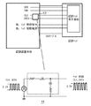
図3は、インクジェットプリンタにおける装置本体と記録ヘッドの間のデータ転送ケーブルによる接続構成を示し、同図において、記録ヘッドは従来とほぼ同様の構成であって、記録装置本体と記録ヘッドとは、ロジック電源電圧VDD、ロジックGND、クロック信号CLK、画像データ信号DATA、その他のヘッド制御信号やヘッド駆動電源などの各信号線がフレキシブルケーブルを介して接続されている。
【0023】
そして、記録装置本体からクロック信号CLKと画像データ信号DATAを記録ヘッドに転送する転送部10にLCR回路11を形成し、このLCR回路11は、各信号CLK,DATAのHIGHレベルを記録ヘッドのロジック電源電圧VDDよりも高い電圧に及び/又はLOWレベルをGNDレベルGNDよりも低い電圧に変換して記録ヘッドに転送する。
【0024】
このHIGHレベルは、VDDが3.3Vに対してLCR回路の設定値を3.6Vとし、LOWレベルについては−0.3VとなるようにLCR回路を設定する。ここで、画像データ信号DATAを送るためのクロック信号CLKの周波数は10MHzを用いる。
【0025】
LCR回路11は、図4に示すように、画像データ信号DATAを転送するためのクロック周波数の帯域に対し、出力対入力の振幅比が1.1倍以上となるように形成される。
【0026】
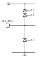
一方、図5に示すように、記録ヘッドの回路基板には、クロック信号CLK、画像データ信号DATAの転送ライン12における、VDDと転送ライン12の間、及び転送ライン12とGNDの間に静電気に対する保護ダイオード13が夫々接続されている。
【0027】
そして、保護ダイオード13が動作するHIGHレベル電圧をVmax、ロジック電源電圧をVDD、クロック信号及び画像データ信号のHIGHレベル電圧をVphとした時、Vmax>Vph>VDDの関係を満たすように記録ヘッドにロジック信号が転送される。
【0028】
また、保護ダイオード13が動作するLOWレベル電圧をVmin、ロジックGNDをVSS、クロック信号及び画像データのLOWレベル電圧をVplとした時、Vmin<Vpl<VSSの関係を満たすように記録ヘッドにロジック信号が転送される。このVmaxは、VDD+1×0.7Vに設定される。
[他の実施形態]
本例は、図6に示すように、記録ヘッドの保護ダイオード13について、VDD側のダイオードを2段に形成して、保護ダイオードが動作する電圧をVDD+0.7VからVDD+1.4Vに増加するように構成している。これは、記録素子と同一基板であっても良いし、記録素子基板と分離している場合は、記録素子を駆動するためのドライバと画像データ信号を受け取るロジック回路とが同時に形成されたICの入力部であっても良い。
【0029】
この実施形態においても、図3と同様に、記録装置本体より記録ヘッドに画像データ信号を転送するためのクロック信号及び画像データ信号を転送する転送部10にLCR回路11を形成して、各信号のHIGHレベルをVDDより高く、及び/又はLOWレベルをGNDより低い電圧を生成して記録ヘッドに信号を供給する。
【0030】
この時のHIGHレベルは、VDDが3.3Vに対してLCR回路の設定値を4.3Vとし、LOWレベルについては上記実施形態と同じ−0.3VとなるようにLCR回路が設定されている。ここでの画像データを送るためのクロック信号の周波数は12MHzに設定される。
【0031】
尚、保護ダイオード13を複数段設けて、さらに入力の振幅を増加させてもよい。
【0032】
なお、以上の実施形態において、記録ヘッドから吐出される液滴はインクであるとして説明し、さらにインクタンクに収容される液体はインクであるとして説明したが、その収容物はインクに限定されるものではない。例えば、記録画像の定着性や耐水性を高めたり、その画像品質を高めたりするために記録媒体に対して吐出される処理液のようなものがインクタンクに収容されていても良い。
【0033】
以上の実施形態は、特にインクジェット記録方式の中でも、インク吐出を行わせるために利用されるエネルギーとして熱エネルギーを発生する手段(例えば電気熱変換体やレーザ光等)を備え、前記熱エネルギーによりインクの状態変化を生起させる方式を用いることにより記録の高密度化、高精細化が達成できる。
【0034】
その代表的な構成や原理については、例えば、米国特許第4723129号明細書、同第4740796号明細書に開示されている基本的な原理を用いて行うものが好ましい。この方式はいわゆるオンデマンド型、コンティニュアス型のいずれにも適用可能であるが、特に、オンデマンド型の場合には、液体(インク)が保持されているシートや液路に対応して配置されている電気熱変換体に、記録情報に対応していて核沸騰を越える急速な温度上昇を与える少なくとも1つの駆動信号を印加することによって、電気熱変換体に熱エネルギーを発生せしめ、記録ヘッドの熱作用面に膜沸騰を生じさせて、結果的にこの駆動信号に1対1で対応した液体(インク)内の気泡を形成できるので有効である。この気泡の成長、収縮により吐出用開口を介して液体(インク)を吐出させて、少なくとも1つの滴を形成する。この駆動信号をパルス形状をすると、即時適切に気泡の成長収縮が行われるので、特に応答性に優れた液体(インク)の吐出が達成でき、より好ましい。
【0035】
このパルス形状の駆動信号としては、米国特許第4463359号明細書、同第4345262号明細書に記載されているようなものが適している。なお、上記熱作用面の温度上昇率に関する発明の米国特許第4313124号明細書に記載されている条件を採用すると、さらに優れた記録を行うことができる。
【0036】
記録ヘッドの構成としては、上述の各明細書に開示されているような吐出口、液路、電気熱変換体の組み合わせ構成(直線状液流路または直角液流路)の他に熱作用面が屈曲する領域に配置されている構成を開示する米国特許第4558333号明細書、米国特許第4459600号明細書を用いた構成も本発明に含まれるものである。加えて、複数の電気熱変換体に対して、共通するスロットを電気熱変換体の吐出部とする構成を開示する特開昭59−123670号公報や熱エネルギーの圧力波を吸収する開口を吐出部に対応させる構成を開示する特開昭59−138461号公報に基づいた構成としても良い。
【0037】
さらに、記録装置が記録できる最大記録媒体の幅に対応した長さを有するフルラインタイプの記録ヘッドとしては、上述した明細書に開示されているような複数記録ヘッドの組み合わせによってその長さを満たす構成や、一体的に形成された1個の記録ヘッドとしての構成のいずれでもよい。
【0038】
加えて、上記の実施形態で説明した記録ヘッド自体に一体的にインクタンクが設けられたカートリッジタイプの記録ヘッドのみならず、装置本体に装着されることで、装置本体との電気的な接続や装置本体からのインクの供給が可能になる交換自在のチップタイプの記録ヘッドを用いてもよい。
【0039】
また、以上説明した記録装置の構成に、記録ヘッドに対する回復手段、予備的な手段等を付加することは記録動作を一層安定にできるので好ましいものである。これらを具体的に挙げれば、記録ヘッドに対してのキャッピング手段、クリーニング手段、加圧あるいは吸引手段、電気熱変換体あるいはこれとは別の加熱素子あるいはこれらの組み合わせによる予備加熱手段などがある。また、記録とは別の吐出を行う予備吐出モードを備えることも安定した記録を行うために有効である。
【0040】
さらに、記録装置の記録モードとしては黒色等の主流色のみの記録モードだけではなく、記録ヘッドを一体的に構成するか複数個の組み合わせによってでも良いが、異なる色の複色カラー、または混色によるフルカラーの少なくとも1つを備えた装置とすることもできる。
【0041】
以上説明した実施の形態においては、インクが液体であることを前提として説明しているが、室温やそれ以下で固化するインクであっても、室温で軟化もしくは液化するものを用いても良く、あるいはインクジェット方式ではインク自体を30°C以上70°C以下の範囲内で温度調整を行ってインクの粘性を安定吐出範囲にあるように温度制御するものが一般的であるから、使用記録信号付与時にインクが液状をなすものであればよい。
【0042】
加えて、積極的に熱エネルギーによる昇温をインクの固形状態から液体状態への状態変化のエネルギーとして使用せしめることで積極的に防止するため、またはインクの蒸発を防止するため、放置状態で固化し加熱によって液化するインクを用いても良い。いずれにしても熱エネルギーの記録信号に応じた付与によってインクが液化し、液状インクが吐出されるものや、記録媒体に到達する時点では既に固化し始めるもの等のような、熱エネルギーの付与によって初めて液化する性質のインクを使用する場合も本発明は適用可能である。このような場合インクは、特開昭54−56847号公報あるいは特開昭60−71260号公報に記載されるような、多孔質シート凹部または貫通孔に液状または固形物として保持された状態で、電気熱変換体に対して対向するような形態としてもよい。本発明においては、上述した各インクに対して最も有効なものは、上述した膜沸騰方式を実行するものである。
【0043】
さらに加えて、本発明に係る記録装置の形態としては、コンピュータ等の情報処理機器の画像出力端末として一体または別体に設けられるものの他、リーダ等と組み合わせた複写装置、さらには送受信機能を有するファクシミリ装置の形態を取るものであっても良い。
【0044】
また、本発明は、複数の機器(例えばホストコンピュータ、インタフェイス機器、リーダ、プリンタなど)から構成されるシステムに適用しても、一つの機器からなる装置(例えば、複写機、ファクシミリ装置など)に適用してもよい。
【0045】
【発明の効果】
以上説明したように、本発明によれば、近年のロジック回路の電源電圧低下に伴って記録ヘッドのロジック電源電圧が低下した中で、クロック信号及び画像データ信号の転送時の振幅を装置本体と記録ヘッドの間で簡単な部品で増加でき、ロジック電源電圧よりも積極的に高い振幅とすることで、従来の高耐圧プロセスとのバランスを保った状態で画像データの転送速度の低下を最小限に抑えることができる。
【図面の簡単な説明】
【図1】本発明の代表的な実施の形態であるインクジェットプリンタIJRAの構成の概要を示す外観斜視図である。
【図2】インクジェットプリンタIJRAの制御回路の構成を示すブロック図である。
【図3】インクジェットプリンタにおける装置本体と記録ヘッドの間のデータ転送ケーブルによる接続構成を示す図である。
【図4】LCR回路の構成を示す図である。
【図5】クロック信号CLK、画像データ信号DATAの転送ラインにおける保護ダイオードの接続構成を示す図である。
【図6】クロック信号CLK、画像データ信号DATAの転送ラインにおける保護ダイオードを複数設けた接続構成を示す図である。
【図7】従来のインクジェット記録ヘッド用基板のレイアウトを示す図である。
【図8】インクジェット記録ヘッド用基板のブロック図である。
【図9】インクジェット記録ヘッド用基板の駆動タイミング例である。
【図10】ロジック電源電圧に対する画像転送可能最大CLK周波数を示す図である。[0001]
BACKGROUND OF THE INVENTION
The present invention, for example, relates to a recording equipment of an ink jet system.
[0002]
[Prior art]
The ink jet recording head is not only an electric energy conversion element such as a heater or a piezoelectric element for discharging ink, but also a driver for driving the element together with the electric energy conversion element, image data, time-division driving, In general, a logic circuit that controls a driver by performing a logical operation while receiving a driving time determination signal is generally built.
[0003]
Conventionally, 5 V has been used as the power supply voltage of the logic circuit. This is because the power supply voltage of an IC such as a CPU and a memory mounted in the ink jet recording apparatus main body is generally 5 V. As a power supply other than a high voltage for driving a recording element such as a heater as the whole ink jet recording apparatus. This is because by unifying at 5 V, it is possible to reduce the size without requiring an extra space for the power supply, and it is possible to reduce the cost of separately preparing a power supply for the logic circuit of the recording head.
[0004]
[Problems to be solved by the invention]
Incidentally, a parallel interface has been generally used as an interface of a conventional printer. In that case, 5V was used as the logic power source of the printer body, and the 5V was also used as the logic power source in the inkjet recording head substrate in the head. In addition, the fact that some of the ICs in the printer internal circuit required a 5V power supply is the background of the characteristics of the inkjet recording head substrate that has been developed with a logic voltage of 5V.
[0005]
However, in recent years, with the improvement of the IC design rule miniaturization technology and the adoption of a new interface, it has been disadvantageous in terms of cost and size to prepare 5V as a logic power source for the printer body. Therefore, there is a movement to adopt 3.3V as the mainstream logic power supply voltage of the printer itself. However, it has been confirmed that some problems occur when the logic power supply voltage of the head substrate, which has been proven so far, is lowered from 5V to 3.3V. This problem will be described below with reference to the drawings.
[0006]
The reduction of the image data transfer capability of the substrate in the ink jet recording head, which is one of the problems, will be described.
[0007]
FIG. 7 shows a configuration example in the substrate for the ink jet recording head. In the figure,
[0008]
The case where a 620-bit heater is formed is described in more detail in FIG. Here, the 620-bit heater is driven at the same time by 40 bits at the maximum, and this is repeated 16 times to drive all the 620-bit heaters (for one cycle). FIG. 9 describes the timing. Here, the speed at which image data needs to be transmitted when all 620 bits are driven at a driving frequency of 15 kHz (also used in existing products) required for performing a constant high-speed recording will be described.
[0009]
15 kHz has a period of 66.67 μS. Within this time, 40-bit image data must be transferred for 16 time divisions (blocks). When this is calculated, the transfer rate of the image data is required to be at least 12 MHz. This speed is not a big value considering the general CPU etc., but in the case of inkjet recording head, if the carriage and the main body are connected by a long flexible board, etc. There was a need that had to be made, and the figure of 12 MHz was never a small value.
[0010]
Under such circumstances, a decrease in transfer capability when the logic power supply voltage is decreased from 5 V to 3.3 V will be described with reference to FIG. FIG. 10A shows the voltage of the logic signal (power supply) and the maximum CLK frequency at which image data can be transferred.
[0011]
As shown in the figure, the CLK frequency tends to decrease as the logic signal (power supply) voltage decreases. This is due to the fact that the driving capability of the MOS transistors used in the input circuit unit such as CLK and the shift register unit for transferring image data is simultaneously reduced by the decrease in the logic power supply voltage used as the gate voltage of the CMOS. By doing. According to the figure, it can be seen that the driving capability (drain current Id) decreases due to a decrease in the gate voltage.
Further, in the ink jet recording head substrate, it is necessary to satisfy the speed in terms of temperature by driving a heater on the substrate. This is a characteristic required for an ink jet recording head substrate that ejects ink with a heater. FIG. 10B shows the relationship between the substrate temperature and the maximum CLK frequency. Here, it shows that there is a tendency for the capacity to decrease further as the temperature increases, as well as a decrease in capacity when the voltage is 3.3V.
[0012]
From the above, it has been found that there has been no problem with a CLK frequency of 12 MHz so far at 5 V, but it is necessary to improve the capacity by 3.3 V.
[0013]
Furthermore, since the recording head is mounted on the carriage and reciprocated, the recording head and the apparatus main body are connected by a long wiring such as a flexible substrate, so that parasitic capacitance is easily added and the amplitude of the logic signal is increased. It is in an environment where it is likely to be smaller when tolerance is taken into consideration than when it is sent from the apparatus main body.
[0014]
The present invention has been made in view of the above problems, its object is to increase the resistance to high current noise during heater drive is to provide a recording equipment that can prevent a decrease in transfer rate such as image data.
[0015]
[Means for Solving the Problems]
To solve the problems described above and achieve the object, a recording apparatus of the present invention includes a plurality of printing elements used for discharging the recording material, the image data and the to drive the plurality of printing elements A plurality of switching elements including a transfer line of a logic signal including a clock signal for transferring image data and a transistor which is provided corresponding to each of the plurality of recording elements and determines whether to energize according to the logic signal. Current applied to the first line having the same potential as the logic power supply potential for controlling the logic circuit or the second line connected to the ground potential when a voltage higher than a threshold is applied to the transfer line. recording head and a protection diode operative to miss, a mountable recording apparatus, the ground and the logic power supply potential A signal generator that generates the logic signal having the same potential difference amplitude as the potential difference between the first and second potentials, and a first potential that is the amplitude of the voltage within the threshold range of the protection diode and higher than the logic power supply potential. A conversion circuit that amplifies the amplitude of the logic signal generated by the signal generation unit and outputs the amplitude to the recording head so that the amplitude is between a second potential lower than the ground potential .
[0018]
DETAILED DESCRIPTION OF THE INVENTION
Hereinafter, an embodiment in which the recording apparatus of the present invention is applied to an ink jet printer will be described in detail with reference to the accompanying drawings.
[Schematic configuration of recording device]
FIG. 1 is an external perspective view showing an outline of the configuration of an ink jet printer IJRA which is a typical embodiment of the present invention. In FIG. 1, the carriage HC engaged with the
[0019]
These capping, cleaning, and suction recovery are configured so that desired processing can be performed at their corresponding positions by the action of the
[0020]
Next, a control configuration for executing the recording control of the above-described apparatus will be described.
FIG. 2 is a block diagram showing the configuration of the control circuit of the inkjet printer IJRA. In the figure, showing a control circuit, 1700 is an interface for inputting a recording signal, 1701 is an MPU, 1702 is a program ROM for storing a control program executed by the
[0021]
The operation of the control configuration will be described. When a recording signal enters the
[0022]
FIG. 3 shows a connection configuration by a data transfer cable between the apparatus main body and the recording head in the ink jet printer. In FIG. 3, the recording head has almost the same configuration as the conventional one. Each signal line such as a logic power supply voltage VDD, a logic GND, a clock signal CLK, an image data signal DATA, other head control signals and a head drive power supply is connected via a flexible cable.
[0023]
The
[0024]
The LCR circuit is set so that the HIGH level is set to 3.6 V with respect to VDD of 3.3 V and the LOW level is set to −0.3 V. Here, the frequency of the clock signal CLK for sending the image data signal DATA is 10 MHz.
[0025]
As shown in FIG. 4, the
[0026]
On the other hand, as shown in FIG. 5, the circuit board of the recording head has a resistance against static electricity between the VDD and the
[0027]
When the HIGH level voltage at which the
[0028]
Further, when the LOW level voltage at which the
[Other Embodiments]
In this example, as shown in FIG. 6, with respect to the
[0029]
Also in this embodiment, the
[0030]
At this time, the LCR circuit is set so that the HIGH level is set to 4.3 V with respect to VDD of 3.3 V, and the LOW level is set to −0.3 V as in the above embodiment. . The frequency of the clock signal for sending the image data here is set to 12 MHz.
[0031]
A plurality of
[0032]
In the above embodiment, the liquid droplets ejected from the recording head have been described as ink, and the liquid stored in the ink tank has been described as ink. However, the storage is limited to ink. It is not a thing. For example, a treatment liquid discharged to the recording medium may be accommodated in the ink tank in order to improve the fixability and water resistance of the recorded image or to improve the image quality.
[0033]
The above embodiment includes means (for example, an electrothermal converter, a laser beam, etc.) that generates thermal energy as energy used for performing ink discharge, particularly in the ink jet recording system, and the ink is generated by the thermal energy. By using a system that causes a change in the state of recording, it is possible to achieve higher recording density and higher definition.
[0034]
As its typical configuration and principle, for example, those performed using the basic principle disclosed in US Pat. Nos. 4,723,129 and 4,740,796 are preferable. This method can be applied to both the so-called on-demand type and continuous type. In particular, in the case of the on-demand type, it is arranged corresponding to the sheet or liquid path holding the liquid (ink). By applying at least one drive signal corresponding to the recorded information and applying a rapid temperature rise exceeding nucleate boiling to the electrothermal transducer, the thermal energy is generated in the electrothermal transducer, and the recording head This is effective because film boiling occurs on the heat acting surface of the liquid, and as a result, bubbles in the liquid (ink) corresponding to the drive signal on a one-to-one basis can be formed. By the growth and contraction of the bubbles, liquid (ink) is ejected through the ejection opening to form at least one droplet. When the drive signal is pulse-shaped, the bubble growth and contraction is performed immediately and appropriately, and thus it is possible to achieve the discharge of liquid (ink) with particularly excellent responsiveness.
[0035]
As this pulse-shaped drive signal, those described in US Pat. Nos. 4,463,359 and 4,345,262 are suitable. Further excellent recording can be performed by employing the conditions described in US Pat. No. 4,313,124 of the invention relating to the temperature rise rate of the heat acting surface.
[0036]
As the configuration of the recording head, in addition to the combination configuration (straight liquid flow path or right-angle liquid flow path) of the discharge port, the liquid path, and the electrothermal transducer as disclosed in each of the above-mentioned specifications, the heat acting surface The configurations using US Pat. No. 4,558,333 and US Pat. No. 4,459,600, which disclose a configuration in which is disposed in a bending region, are also included in the present invention. In addition, Japanese Patent Application Laid-Open No. 59-123670, which discloses a configuration in which a common slot is used as a discharge portion of an electrothermal transducer, or an opening that absorbs a pressure wave of thermal energy is discharged to a plurality of electrothermal transducers. A configuration based on Japanese Patent Laid-Open No. 59-138461 disclosing a configuration corresponding to each part may be adopted.
[0037]
Furthermore, as a full-line type recording head having a length corresponding to the width of the maximum recording medium that can be recorded by the recording apparatus, the length is satisfied by a combination of a plurality of recording heads as disclosed in the above specification. Either a configuration or a configuration as a single recording head formed integrally may be used.
[0038]
In addition to the cartridge-type recording head in which the ink tank is integrally provided in the recording head itself described in the above embodiment, it can be electrically connected to the apparatus body by being attached to the apparatus body. A replaceable chip type recording head that can supply ink from the apparatus main body may be used.
[0039]
In addition, it is preferable to add recovery means, preliminary means, and the like for the recording head to the configuration of the recording apparatus described above because the recording operation can be further stabilized. Specific examples thereof include a capping unit for the recording head, a cleaning unit, a pressurizing or sucking unit, an electrothermal converter, a heating element different from this, or a preheating unit using a combination thereof. In addition, it is effective to provide a preliminary ejection mode for performing ejection different from recording in order to perform stable recording.
[0040]
Further, the recording mode of the recording apparatus is not limited to the recording mode of only the mainstream color such as black, but the recording head may be integrated or may be a combination of a plurality of colors. An apparatus having at least one of full colors can also be provided.
[0041]
In the embodiment described above, the description is made on the assumption that the ink is a liquid, but it may be an ink that is solidified at room temperature or lower, or an ink that is softened or liquefied at room temperature, Alternatively, the ink jet method generally controls the temperature of the ink so that the viscosity of the ink is within a stable discharge range by adjusting the temperature within a range of 30 ° C. or higher and 70 ° C. or lower. It is sufficient if the ink sometimes forms a liquid.
[0042]
In addition, it is solidified in a stand-by state in order to actively prevent temperature rise by heat energy as energy for changing the state of ink from the solid state to the liquid state, or to prevent ink evaporation. Ink that is liquefied by heating may be used. In any case, by applying heat energy according to a recording signal of thermal energy, the ink is liquefied and liquid ink is ejected, or when it reaches the recording medium, it already starts to solidify. The present invention can also be applied to the case where ink having a property of being liquefied for the first time is used. In such a case, the ink is held as a liquid or solid in a porous sheet recess or through-hole as described in JP-A-54-56847 or JP-A-60-71260, It is good also as a form which opposes with respect to an electrothermal converter. In the present invention, the most effective one for each of the above-described inks is to execute the above-described film boiling method.
[0043]
In addition, as a form of the recording apparatus according to the present invention, a copying apparatus combined with a reader or the like, and a transmission / reception function are provided as an image output terminal of an information processing apparatus such as a computer or the like. It may take the form of a facsimile machine.
[0044]
In addition, the present invention can be applied to a system composed of a plurality of devices (for example, a host computer, interface device, reader, printer, etc.), or a device (for example, a copier, a facsimile device, etc.) composed of a single device. You may apply to.
[0045]
【The invention's effect】
As described above, according to the present invention, while the logic power supply voltage of the recording head has decreased with the recent decrease in the power supply voltage of the logic circuit, the amplitude at the time of transfer of the clock signal and the image data signal can be It can be increased with simple parts between recording heads, and the amplitude is positively higher than the logic power supply voltage, minimizing the decrease in image data transfer speed while maintaining a balance with the conventional high voltage process. Can be suppressed.
[Brief description of the drawings]
FIG. 1 is an external perspective view showing an outline of the configuration of an inkjet printer IJRA that is a representative embodiment of the present invention.
FIG. 2 is a block diagram illustrating a configuration of a control circuit of the inkjet printer IJRA.
FIG. 3 is a diagram illustrating a connection configuration using a data transfer cable between an apparatus main body and a recording head in an inkjet printer.
FIG. 4 is a diagram illustrating a configuration of an LCR circuit.
FIG. 5 is a diagram illustrating a connection configuration of protection diodes in a transfer line of a clock signal CLK and an image data signal DATA.
FIG. 6 is a diagram showing a connection configuration in which a plurality of protection diodes are provided in a transfer line for a clock signal CLK and an image data signal DATA.
FIG. 7 is a diagram showing a layout of a conventional inkjet recording head substrate.
FIG. 8 is a block diagram of an inkjet recording head substrate.
FIG. 9 is an example of drive timing of the inkjet recording head substrate.
FIG. 10 is a diagram illustrating a maximum CLK frequency at which an image can be transferred with respect to a logic power supply voltage.
Claims (13)
前記複数の記録素子を駆動するための画像データ及び該画像データを転送するためのクロック信号を含むロジック信号の転送ラインと、
前記複数の記録素子の其々に対応して設けられ、前記ロジック信号によって通電するかを決定するトランジスタからなる複数のスイッチング素子を有するロジック回路と、
前記転送ラインに閾値以上の電圧が印加されたときに、前記ロジック回路を制御するためのロジック電源電位と同電位の第一ラインまたは接地電位に接続する第二ラインに電流を逃すように動作する保護ダイオードと、
を備えた記録ヘッドを、搭載可能な記録装置であって、
前記ロジック電源電位と前記接地電位との電位差と同じ電位差の振幅を有する前記ロジック信号を生成する信号生成部と、
前記保護ダイオードの前記閾値の範囲内の電圧の振幅であり、かつ、前記ロジック電源電位より高い第一電位と前記接地電位より低い第二電位との間の振幅となるように、前記信号生成部で生成された前記ロジック信号の振幅を増幅して前記記録ヘッドに出力する変換回路と、
を有することを特徴とする記録装置。A plurality of recording elements used for discharging the recording agent ;
A transfer line for logic signals including a clock signal for transferring the image data and the image data for driving the plurality of recording elements,
A logic circuit that is provided corresponding to each of the plurality of recording elements and includes a plurality of switching elements including transistors that determine whether to energize according to the logic signal;
When a voltage equal to or higher than a threshold is applied to the transfer line, it operates so as to release current to the first line having the same potential as the logic power supply potential for controlling the logic circuit or the second line connected to the ground potential. A protective diode;
A recording apparatus capable of mounting a recording head comprising:
A signal generation unit that generates the logic signal having the same potential difference amplitude as the potential difference between the logic power supply potential and the ground potential;
The signal generator has an amplitude of a voltage within the threshold range of the protection diode and an amplitude between a first potential higher than the logic power supply potential and a second potential lower than the ground potential. A conversion circuit that amplifies the amplitude of the logic signal generated in step (a) and outputs the amplified signal to the recording head;
A recording apparatus comprising:
前記電源生成部で生成された前記ロジック電源電位は、前記信号生成部において前記ロジック信号の生成にも用いられることを特徴とする請求項1に記載の記録装置。The recording apparatus according to claim 1, wherein the logic power supply potential generated by the power generation unit is also used for generation of the logic signal by the signal generation unit.
前記保護ダイオードが動作するLOWレベル電圧をVmin、ロジックGNDをVSS、前記変換回路で増幅されたクロック信号及び画像データのLOWレベル電圧をVplとした時、Vmin<Vpl<VSSの関係を満たすように増幅することを特徴とする請求項1乃至5のいずれか1項に記載の記録装置。 The conversion circuit is Vmax>Vph>, where Vmax is the HIGH level voltage at which the protection diode operates, VDD is the logic power supply voltage, and Vph is the HIGH level voltage of the clock signal and image data signal amplified by the conversion circuit. meet the relationship VDD, and,
When the LOW level voltage at which the protection diode operates is Vmin, the logic GND is VSS, and the clock signal amplified by the conversion circuit and the LOW level voltage of the image data are Vpl, Vmin <Vpl <VSS is satisfied. The recording apparatus according to claim 1, wherein the recording apparatus amplifies the recording apparatus.
Priority Applications (1)
| Application Number | Priority Date | Filing Date | Title |
|---|---|---|---|
| JP2001182524A JP4636737B2 (en) | 2001-06-15 | 2001-06-15 | Recording device |
Applications Claiming Priority (1)
| Application Number | Priority Date | Filing Date | Title |
|---|---|---|---|
| JP2001182524A JP4636737B2 (en) | 2001-06-15 | 2001-06-15 | Recording device |
Publications (2)
| Publication Number | Publication Date |
|---|---|
| JP2002370359A JP2002370359A (en) | 2002-12-24 |
| JP4636737B2 true JP4636737B2 (en) | 2011-02-23 |
Family
ID=19022616
Family Applications (1)
| Application Number | Title | Priority Date | Filing Date |
|---|---|---|---|
| JP2001182524A Expired - Fee Related JP4636737B2 (en) | 2001-06-15 | 2001-06-15 | Recording device |
Country Status (1)
| Country | Link |
|---|---|
| JP (1) | JP4636737B2 (en) |
Citations (5)
| Publication number | Priority date | Publication date | Assignee | Title |
|---|---|---|---|---|
| JPH0365059U (en) * | 1989-10-27 | 1991-06-25 | ||
| JPH04369262A (en) * | 1991-06-17 | 1992-12-22 | Olympus Optical Co Ltd | Cmos semiconductor device and manufacture thereof |
| JPH08137346A (en) * | 1994-11-09 | 1996-05-31 | Ricoh Co Ltd | Image forming device |
| JPH09321149A (en) * | 1996-05-28 | 1997-12-12 | Nkk Corp | Semiconductor device having input/output protection circuit |
| JPH10143341A (en) * | 1996-09-05 | 1998-05-29 | Ricoh Co Ltd | Image forming system and its controlling method, peripheral equipment and its controlling method, peripheral equipment interface switching device and its controlling method, and interface, computer, and recording medium for peripheral equipment |
-
2001
- 2001-06-15 JP JP2001182524A patent/JP4636737B2/en not_active Expired - Fee Related
Patent Citations (5)
| Publication number | Priority date | Publication date | Assignee | Title |
|---|---|---|---|---|
| JPH0365059U (en) * | 1989-10-27 | 1991-06-25 | ||
| JPH04369262A (en) * | 1991-06-17 | 1992-12-22 | Olympus Optical Co Ltd | Cmos semiconductor device and manufacture thereof |
| JPH08137346A (en) * | 1994-11-09 | 1996-05-31 | Ricoh Co Ltd | Image forming device |
| JPH09321149A (en) * | 1996-05-28 | 1997-12-12 | Nkk Corp | Semiconductor device having input/output protection circuit |
| JPH10143341A (en) * | 1996-09-05 | 1998-05-29 | Ricoh Co Ltd | Image forming system and its controlling method, peripheral equipment and its controlling method, peripheral equipment interface switching device and its controlling method, and interface, computer, and recording medium for peripheral equipment |
Also Published As
| Publication number | Publication date |
|---|---|
| JP2002370359A (en) | 2002-12-24 |
Similar Documents
| Publication | Publication Date | Title |
|---|---|---|
| US7802858B2 (en) | Element board for printhead, printhead and printhead control method | |
| JP4989433B2 (en) | Head substrate, recording head, head cartridge, and recording apparatus | |
| EP1543972B1 (en) | Element board for printhead, and printhead having the same | |
| US6471324B1 (en) | Printhead with malfunction prevention function and printing apparatus using it | |
| JP4666818B2 (en) | RECORDING HEAD, RECORDING HEAD CARTRIDGE, AND RECORDING DEVICE THEREOF | |
| JP4859213B2 (en) | Element base of recording head, recording head, recording apparatus | |
| EP1142715A1 (en) | Printhead as well as printing apparatus comprising such printhead | |
| US6382755B1 (en) | Printhead and printing apparatus using printhead | |
| EP1266760B1 (en) | Printhead, head cartridge having said printhead, printing apparatus using said printhead and printhead element substrate | |
| US6712437B2 (en) | Printhead board, printhead and printing apparatus | |
| JP4035253B2 (en) | Recording head and recording apparatus using the recording head | |
| JP4636737B2 (en) | Recording device | |
| JP4724272B2 (en) | Recording head and recording apparatus using the recording head | |
| JP3517612B2 (en) | Ink jet recording head and recording device | |
| JP2001246751A (en) | Recording head, recording apparatus with the recording head, and method for driving recording head | |
| JP4208431B2 (en) | Recording head and recording apparatus using the recording head | |
| JP3884924B2 (en) | Printhead heater board | |
| JP2002370362A (en) | Recording head, head cartridge having the recording head, recorder using the recording head, and recording head element substrate | |
| JP2002011883A (en) | Recording method and recording apparatus | |
| JP2002370358A (en) | Recording head and recorder using it | |
| JP2000043268A (en) | Recording head and recorder employing it | |
| JP2005047229A (en) | Control circuit, driving circuit, and recording device | |
| JPH1178019A (en) | Recording head, recorder employing it, driving method for recording head, and recording head cartridge |
Legal Events
| Date | Code | Title | Description |
|---|---|---|---|
| A621 | Written request for application examination |
Free format text: JAPANESE INTERMEDIATE CODE: A621 Effective date: 20080616 |
|
| A131 | Notification of reasons for refusal |
Free format text: JAPANESE INTERMEDIATE CODE: A131 Effective date: 20100906 |
|
| A521 | Written amendment |
Free format text: JAPANESE INTERMEDIATE CODE: A523 Effective date: 20101028 |
|
| TRDD | Decision of grant or rejection written | ||
| A01 | Written decision to grant a patent or to grant a registration (utility model) |
Free format text: JAPANESE INTERMEDIATE CODE: A01 Effective date: 20101115 |
|
| A01 | Written decision to grant a patent or to grant a registration (utility model) |
Free format text: JAPANESE INTERMEDIATE CODE: A01 |
|
| A61 | First payment of annual fees (during grant procedure) |
Free format text: JAPANESE INTERMEDIATE CODE: A61 Effective date: 20101122 |
|
| FPAY | Renewal fee payment (event date is renewal date of database) |
Free format text: PAYMENT UNTIL: 20131203 Year of fee payment: 3 |
|
| R150 | Certificate of patent or registration of utility model |
Free format text: JAPANESE INTERMEDIATE CODE: R150 |
|
| LAPS | Cancellation because of no payment of annual fees |