JP4635286B2 - Semiconductor device - Google Patents
Semiconductor device Download PDFInfo
- Publication number
- JP4635286B2 JP4635286B2 JP33395899A JP33395899A JP4635286B2 JP 4635286 B2 JP4635286 B2 JP 4635286B2 JP 33395899 A JP33395899 A JP 33395899A JP 33395899 A JP33395899 A JP 33395899A JP 4635286 B2 JP4635286 B2 JP 4635286B2
- Authority
- JP
- Japan
- Prior art keywords
- type impurity
- impurity diffusion
- diffusion region
- type
- gate electrode
- Prior art date
- Legal status (The legal status is an assumption and is not a legal conclusion. Google has not performed a legal analysis and makes no representation as to the accuracy of the status listed.)
- Expired - Fee Related
Links
Images

Landscapes
- Electrodes Of Semiconductors (AREA)
Description
【0001】
【発明の属する技術分野】
本発明は、ゲート電極を備えた半導体装置に関する。
【0002】
【従来の技術】
近年、MOSFET(Metal Oxide SemiconductorField Effect Transistor)やIGBT(Insulated Gate Bipolar Transistor)等のゲート電極を備えた半導体装置は、高速スイッチング特性を備えているため様々な分野に広く用いられている。特にIGBTは、MOSFETの高速スイッチング特性とバイポーラトランジスタの高出力特性を兼ね備えており、パワーエレクトロニクスの分野で多く用いられている。
【0003】
ゲート電極を備えた半導体装置として、図8に従来のIGBT500の断面図が示されている。
【0004】
p型高濃度半導体基板2上にn型高濃度ドリフト層4が選択的に形成されている。このn型高濃度ドリフト層4には、n型低濃度ドリフト領域6が選択的に形成されている。このn型低濃度ドリフト領域6表面には、p型ボディ領域8が形成されている。このp型ボディ領域8の表面にはn型エミッタ領域10が形成されている。そして、ゲート絶縁膜12を介して、n型低濃度ドリフト領域6上及びp型ボディ領域8上にゲート電極84が形成されている。一方、n型エミッタ領域10に接触するようにエミッタ電極16が形成され、p型高濃度半導体基板2の裏面側には、コレクタ電極18が形成される。
【0005】
このIGBT500の動作は原理は以下の通りである。IGBT500を導通させるとき(導通時)には、ゲート電極84にエミッタ電極16に対して正の電圧(正のバイアス電圧)が印加される。ゲート電極84に正のバイアス電圧が印加されると、p型ボディ領域8の表面にn型チャネルが形成され、n型エミッタ領域10からn型低濃度ドリフト領域6及びn型高濃度ドリフト層4へ多数キャリアが注入される。n型低濃度ドリフト領域6及びn型高濃度ドリフト層4へ多数キャリアが注入されると、p型高濃度半導体基板2側から、少数キャリアがn型高濃度ドリフト層4及びn型低濃度ドリフト領域6へ注入され、エミッタ電極16とコレクタ電極18との間に電流が流れる。
【0006】
一方、IGBT500を導通させないとき(非導通時)には、ゲート電極84にエミッタ電極16に対して負の電圧(負のバイアス電圧)が印加される。これにより、前述したn型チャネルが消失し、エミッタ電極16とコレクタ電極18との間に電流が流れなくなる。
【0007】
IGBT500の導通時及び非導通時のエネルギーバンド図が、図9に示されている。図9(a)及び図9(b)には、p型ボディ領域8表面、ゲート絶縁膜12及びゲート電極84のエネルギーバンド図が示されている。また、図9(c)及び(d)には、n型低濃度ドリフト領域6表面及びゲート電極84のエネルギーバンド図が示されている。
【0008】
図9において、qФMはゲート電極84の材料の仕事関数、EFはフェルミ準位、VACは真空準位、Ecは伝導帯下端、Evは価電子帯上端を示している。
【0009】
非導通時(ゲートバイアス電圧Vg=0)では、図9(a)に示されているように、ゲート絶縁膜を介して、ゲート電極とp型ボディ領域とのフェルミ準位が等しくなるように平衡が保たれている。
【0010】
ところが、導通時(Vg>0)となると、図9(b)に示されているように、ゲート電極側のフェルミ準位が下がり、p型ボディ領域側では、p型ボディ領域とゲート絶縁膜との界面で伝導体下端が曲がり、少数キャリア(電子)が蓄積される。
【0011】
非導通時(ゲートバイアス電圧Vg=0)では、図9(c)に示されているように、絶縁膜を介して、ゲート電極とn型低濃度ドリフト領域とのフェルミ準位が等しくなるように平衡が保たれている。
【0012】
一方、導通時(Vg>0)になると、図9(d)に示されているように、ゲート電極側のフェルミ準位が下がり、n型低濃度ドリフト領域側では、n型低濃度ドリフト領域とゲート絶縁膜との界面で伝導体下端が曲がり、多数キャリア(電子)が蓄積される。
【0013】
【発明が解決しようとする課題】
ところで、IGBT500の導通時には、ゲート電極84に正のバイアス電圧が印加されるため、p型ボディ領域8とn型低濃度ドリフト領域6との間の空乏層が濃度の低いn型低濃度ドリフト領域6側へ延びる。この空乏層のために、n型エミッタ領域10側から注入される多数キャリア(電子)が流れる電流路が狭くなり、n型低濃度ドリフト領域6及びn型高濃度ドリフト層4における抵抗(ジャンクションFET抵抗、JFET抵抗)成分が大きくなってしまう。
【0014】
また、JFET抵抗を減らすために、P型ボディ領域8の拡散深さを浅くするとIGBT500がラッチアップを起こしやすくなり、破壊耐量が低下するという問題があった。
【0015】
本発明は、上記課題を解決するためになされたものであり、破壊耐量が大きく、低損失な半導体装置を提供することを目的とする。
【0016】
【課題を解決するための手段】
本発明は、半導体基板内に形成された第1のn型不純物拡散領域と、前記第1の第1導電型不純物拡散領域表面に形成されたp型不純物拡散領域と、前記第2導電型不純物拡散領域表面に形成された第2のn型不純物拡散領域と、ゲート絶縁膜を介して、少なくとも前記第1のn型不純物拡散領域と前記p型不純物拡散領域に隣接するゲート電極と、前記第2のn型不純物拡散領域からp型不純物拡散領域を介して前記第1のn型不純物拡散領域に達するように形成された溝と、を備え、前記ゲート電極は、前記ゲート絶縁膜を介して前記溝内壁に形成されており、前記ゲート電極に電圧を印加したときに、前記第1のn型不純物拡散領域のゲート絶縁膜との界面での伝導体下端の曲がりが、前記p型不純物拡散領域の伝導体下端の曲がりよりも大きくなるように、前記ゲート電極の前記第1のn型不純物拡散領域に隣接する第1部位の材料が有する第1部位仕事関数を、前記ゲート電極の前記p型不純物拡散領域に隣接する第2部位の材料が有する第2部位仕事関数よりも小さくし、且つ前記第1部位をn型不純物ポリシリコンで、前記第2部位をp型不純物ポリシリコンでそれぞれ構成することを特徴とする。
また、本発明の別の形態は、半導体基板内に形成された第1のp型不純物拡散領域と、前記第1の第1導電型不純物拡散領域表面に形成されたn型不純物拡散領域と、前記第2導電型不純物拡散領域表面に形成された第2のp型不純物拡散領域と、ゲート絶縁膜を介して、少なくとも前記第1のp型不純物拡散領域と前記p型不純物拡散領域に隣接するゲート電極と、前記第2のp型不純物拡散領域からn型不純物拡散領域を介して前記第1のp型不純物拡散領域に達するように形成された溝と、を備え、前記ゲート電極は、前記ゲート絶縁膜を介して前記溝内壁に形成されており、前記ゲート電極に電圧を印加したときに、前記第1のp型不純物拡散領域のゲート絶縁膜との界面での伝導体下端の曲がりが、前記n型不純物拡散領域の伝導体下端の曲がりよりも大きくなるように、前記ゲート電極の前記第1のp型不純物拡散領域に隣接する第1部位の材料が有する第1部位仕事関数を、前記ゲート電極の前記n型不純物拡散領域に隣接する第2部位の材料が有する第2部位仕事関数よりも大きくし、且つ前記第1部位をp型不純物ポリシリコンで、前記第2部位をn型不純物ポリシリコンでそれぞれ構成することを特徴とする。
【0017】
上記構成によれば、半導体装置の導通時に、第1の第1導電型(例えば、n型)不純物拡散領域のゲート電極に隣接する部位に蓄積される多数キャリア量が多くなる。そのため、第1の第1導電型不純物拡散領域と第2導電型(例えば、p型)不純物拡散領域との接合部の空乏層の第1の第1導電型不純物拡散領域側への延びが抑えられ、JFET抵抗を減らすことができる。また、第1の第1導電型不純物拡散領域のゲート電極に隣接する部位に蓄積される多数キャリア量が多くなり、第1の第1導電型不純物拡散領域に注入される少数キャリア量が増えるため、第1の第1導電型不純物拡散領域自体の抵抗を減らすことができる。したがって、低損失な半導体装置を提供することが可能である。
【0021】
【発明の実施の形態】
以下、本発明の実施の形態(以下実施形態という)を、図面に従って説明する。尚、各図を通じて、同じ部材には同一の符号が付されている。
【0022】
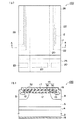
図1には、本実施形態の半導体装置であるIGBT100が示されている。図1(a)には、IGBT100の平面図が示されており、図1(b)には、図1(a)におけるAA線での断面図が示されている。p型高濃度半導体基板2上にn型高濃度ドリフト層4が選択的に形成されている。このn型高濃度ドリフト層4の表面には、n型低濃度ドリフト領域6が選択的に形成されている。このn型低濃度ドリフト領域6表面には、p型ボディ領域8が形成されている。このp型ボディ領域8の表面にはn型エミッタ領域10が形成されている。そして、ゲート絶縁膜12を介して、少なくともn型低濃度ドリフト領域6及びp型ボディ領域8に隣接するようにポリシリコンを材料とするゲート電極14が形成されている。一方、n型エミッタ領域10に接触するようにエミッタ電極16が形成される。エミッタ電極16は、層間絶縁膜17によって、ゲート電極14と電気的に絶縁されている。p型高濃度半導体基板2の裏面側には、コレクタ電極18が形成される。ゲート電極14は、コンタクト20を介してゲート用アルミ電極24に接続されている。また、エミッタ電極16は、コンタクト22を介してエミッタ用アルミ電極26に接続されている。
【0023】
ゲート電極14は、n型低濃度ドリフト領域6に隣接する第1部位30と、p型ボディ領域8に隣接する第2部位32とを備えている。この第1部位30と第2部位32はポリシリコンを材料としているが、各々不純物濃度が異なっているので、各々仕事関数も異なっている。
【0024】
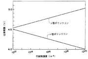
図2には、ポリシリコン中の不純物濃度と仕事関数との関係が示されている。
横軸が不純物濃度を示し、縦軸が仕事関数を示している。ポリシリコン中にヒ素やリン等の不純物を注入し、ポリシリコンをn型にした場合(図2中のn型ポリシリコンの場合)、ポリシリコン中の不純物濃度を高くすると仕事関数が小さくなる。ポリシリコン中にホウ素等の不純物を注入し、ポリシリコンをp型にした場合(図2中のp型ポリシリコンの場合)、ポリシリコン中の不純物濃度を高くすると仕事関数が小さくなる。
【0025】
図2に示された関係を利用して、ゲート電極14の第1部位30のポリシリコン中の不純物濃度と、第2部位32のポリシリコン中の不純物濃度とを、異ならせることによって、第1部位30のポリシリコンと第2部位32のポリシリコンとの仕事関数を変えることができる。
【0026】
本実施形態では、ゲート電極14の第1部位30のポリシリコンのみに不純物としてヒ素を注入し、第1部位30のポリシリコンをn型の導電型にし、第1部位30の仕事関数を第2部位32の仕事関数より小さくしている。尚、第2部位32に不純物としてホウ素を注入することで、第2部位の仕事関数をより大きくし、第1部位30と第2部位32の仕事関数差を大きくしてもよい。
【0027】
このように、第1部位30の仕事関数を第2部位32の仕事関数より小さくすることで、IGBT100の導通時にn型低濃度ドリフト領域6に蓄積される多数キャリア(電子)の量を増やすことができる。
【0028】
次に、IGBT100の導通時のエネルギーバンドの様子を説明することで、n型低濃度ドリフト領域6に蓄積される多数キャリア(電子)の量が増える原理を説明する。
【0029】
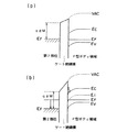
図3には、p型ボディ領域8表面及びゲート電極14の第2部位32でのエネルギーバンド図が示されている。図3において、qФMはゲート電極14の第2部位32の材料の仕事関数、EFはフェルミ準位、VACは真空準位、Ecは伝導帯下端、Evは価電子帯上端を示している。
【0030】
非導通時(ゲートバイアス電圧Vg=0)では、図3(a)に示されているように、ゲート絶縁膜を介して、ゲート電極の第2部位とp型ボディ領域とのフェルミ準位が等しくなるように平衡が保たれている。
【0031】
ところが、導通時(Vg>0)となると、図3(b)に示されているように、ゲート電極側のフェルミ準位が下がり、p型ボディ領域側では、p型ボディ領域とゲート絶縁膜との界面で伝導体下端Ecが曲がり、電子が蓄積される。
【0032】
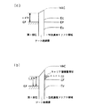
一方、図4には、本実施形態のゲート電極の第1部位の材料の仕事関数が第2部位の材料の仕事関数より小さい場合のn型低濃度ドリフト領域6表面及びゲート電極の第1部位のエネルギーバンド図が示されている。ここで、qФ’Mを第1部位30の材料の仕事関数とする。
【0033】
非導通状態(ゲートバイアス電圧Vg=0)では、図4(a)に示されているように、ゲート絶縁膜を介して、ゲート電極とn型低濃度ドリフト領域とのフェルミ準位が等しくなるように平衡が保たれている。しかし、ゲート電極の第1部位の材料の仕事関数が第2部位の材料の仕事関数と同じ場合(図9(c))と比較すると、伝導帯下端Ecが大きく曲がっている。
【0034】
一方、導通状態(Vg>0)となると、図4(b)に示されているように、ゲート電極側のフェルミ準位が上がり、n型低濃度ドリフト領域側では、n型低濃度ドリフト領域とゲート絶縁膜との界面で伝導帯下端Ecが曲がり、多数キャリア(電子)が蓄積される。この伝導帯下端Ecの曲がりは、ゲート電極の第1部位の材料の仕事関数が第2部位の材料の仕事関数と同じ場合(図9(d))と比較すると大きくなり、より多くのキャリア(電子)を蓄積することができる。
【0035】
このように、本実施形態においては、ゲート電極14の第1部位30の材料の仕事関数と、ゲート電極14の第2部位32の材料の仕事関数とが異なっており、第1部位30の材料の仕事関数のほうが、第2部位32の仕事関数より小さい。したがって、n型低濃度ドリフト領域6表面のエネルギーバンドの曲がりが大きくなり、n型低濃度ドリフト領域6表面に蓄積される多数キャリア(電子)の量を増やすことができる。したがって、p型ボディ領域8とn型低濃度ドリフト領域6との接合部の空乏層がn型低濃度ドリフト領域6側に延びるのを抑えることができ、JFET抵抗を下げることができる。また、表面に多数キャリア(電子)が多くなるので、コレクタ電極から少数キャリア(正孔)が多く注入され、見かけ上、n型低濃度ドリフト領域6の抵抗を下げることができる。
【0036】
図5には、他の実施形態の半導体装置として、溝(トレンチ)を備えたIGBT200が示されている。図5(a)には、IGBT200の平面図が示されており、図5(b)には、図5(a)におけるBB線での断面図が示されている。このIGBT200は、n型エミッタ領域10からp型ボディ領域8を介してn型低濃度ドリフト領域6へ達するトレンチ50を備えている。このトレンチ50内に、ゲート電極14が形成されている。このゲート電極14は、n型低濃度ドリフト領域6に隣接する第1部位30と、p型ボディ領域8に隣接する第2部位32とを備えている。この第1部位30と第2部位32はポリシリコンを材料としているが、各々不純物濃度が異なっているため、各々仕事関数が異なっている。このように、ゲート電極14の第1部位30のポリシリコン中の不純物濃度と第2部位32のポリシリコン中の不純物濃度とを異ならせることによって、第1部位30のポリシリコンと第2部位32のポリシリコンとの仕事関数を変えることができる。このとき、第1部位30の材料の仕事関数を第2部位32の材料の仕事関数より小さくすると、導通時にn型低濃度ドリフト領域6に蓄積される多数キャリア(電子)の量を増やし、n型低濃度ドリフト領域6の抵抗を減らすことができる。
【0037】
前述した実施形態においては、ゲート電極14内部にポリシリコンより抵抗値が小さい別の金属を材料とし、抵抗率が低い異種金属層をCVD法等を用いて形成するのも好適である。図6には、ゲート電極14内に異種金属層60を備えたIGBT300の断面図が示されている。異種金属層60は抵抗値が小さいため、ゲート入力抵抗を下げることができる。
【0038】
前述した実施形態において、各領域においてn型をp型の導電型に、p型をn型の導電型にしてもよい。図7には、図1において導電型を逆にしたIGBT400の断面図が示されている。n型高濃度半導体基板102上にp型高濃度ドリフト層104が選択的に形成されている。このp型高濃度ドリフト層104には、p型低濃度ドリフト領域106が選択的に形成されている。このp型低濃度ドリフト領域106の表面には、n型ボディ領域108が形成されている。このn型ボディ領域108の表面にはp型エミッタ領域110が形成されている。そして、ゲート絶縁膜112を介して、p型低濃度ドリフト領域106及びn型ボディ領域108に隣接するようにポリシリコンを材料とするゲート電極114が形成されている。一方、p型エミッタ領域110に接触するようにエミッタ電極116が形成され、n型高濃度半導体基板102の裏面側には、コレクタ電極118が形成される。
【0039】
ゲート電極114は、p型低濃度ドリフト領域106に隣接する第1部位130と、n型ボディ領域108に隣接する第2部位132とを備えている。この第1部位130及び第2部位132はポリシリコンを材料としているが、各々不純物濃度が異なっており、各々仕事関数も異なっている。このとき、第1部位130の仕事関数を第2部位132の仕事関数より大きく設定することが好適である。
【0040】
ゲート電極114の第1部位130の材料の仕事関数よりゲート電極114の第2部位132の材料の仕事関数が大きいため、p型低濃度ドリフト領域106の伝導体下端が大きく曲がり、多数キャリア(正孔)を多く蓄積することができる。そのため、n型ボディ領域108とp型低濃度ドリフト領域106との接合部の空乏層がp型低濃度ドリフト領域106側に延びるのを抑えることができ、JFET抵抗を下げることができる。また、表面に多数キャリア(正孔)が多くなるので、コレクタ電極118から少数キャリア(電子)が多く注入され、見かけ上、p型低濃度ドリフト領域106の抵抗を下げることができる。
【0041】
各実施形態では、半導体装置としてIGBTを例示したが、IGBTに限定したものではなく、MOSFET等のゲート電極と2つの同一導電型の不純物拡散領域と、その2つの領域に挟まれた1つの他の導電型の不純物拡散領域とを備えた電解効果トランジスタ等に適用することが可能である。
【0042】
【発明の効果】
本発明においては、第1の第1導電型不純物拡散領域にゲート絶縁膜を介して隣接するゲート電極の第1部位と、第2導電型不純物拡散領域にゲート絶縁膜を介して隣接するゲート電極の第2部位との仕事関数を適宜設定することができる。したがって、半導体装置の導通時に、第1の第1導電型不純物拡散領域のゲート電極の隣接する部位に蓄積される多数キャリア量が多くなる。そのため、第1の第1導電型不純物拡散領域と第2導電型不純物拡散領域との接合部の空乏層の第1の第1導電型不純物拡散領域側への延びが抑えられ、JFET抵抗を減らすことができる。また、第1の第1導電型不純物拡散領域のゲート電極の隣接する部位に蓄積される多数キャリア量が多くなり、第1の第1導電型不純物拡散領域に注入される少数キャリア量が増えるため、第1の第1導電型不純物拡散領域自体の抵抗を減らすことができる。したがって、低損失な半導体装置を提供することが可能である。
【図面の簡単な説明】
【図1】 本実施形態のIGBTが示された図である。
【図2】 ポリシリコンの不純物濃度と仕事関数との関係が現れた図である。
【図3】 本実施形態のIGBTのp型ボディ領域表面とゲート電極14の第2部位におけるエネルギーバンドが示された図である。
【図4】 本実施形態のIGBTのn型ボディ領域表面とゲート電極14の第2部位におけるエネルギーバンドが示された図である。
【図5】 他の実施形態のIGBTが示された図である。
【図6】 他の実施形態のIGBTが示された図である。
【図7】 導電型異なった他の実施形態のIGBTが示された図である。
【図8】 従来のIGBTが示された図である。
【図9】 従来のIGBTのp型ボディ領域表面、n型低濃度ドリフト領域表面及びゲート電極におけるエネルギーバンドが示された図である。
【符号の説明】
2 p型高濃度半導体基板、6 n型低濃度ドリフト領域、8 p型ボディ領域、12,112 ゲート絶縁膜、14,84,114 ゲート電極、30,130 第1部位、32,132 第2部位、100,200,300,400 500 IGBT、102 n型高濃度半導体基板、106 p型低濃度ドリフト領域、108 n型ボディ領域。[0001]
BACKGROUND OF THE INVENTION
The present invention relates to a semiconductor device provided with a gate electrode.
[0002]
[Prior art]
In recent years, semiconductor devices including gate electrodes such as MOSFETs (Metal Oxide Semiconductor Field Effect Transistors) and IGBTs (Insulated Gate Bipolar Transistors) have been widely used in various fields because they have high-speed switching characteristics. In particular, IGBTs have both high-speed switching characteristics of MOSFETs and high output characteristics of bipolar transistors, and are often used in the field of power electronics.
[0003]
As a semiconductor device provided with a gate electrode, a cross-sectional view of a
[0004]
An n-type high
[0005]
The principle of the operation of the IGBT 500 is as follows. When the
[0006]
On the other hand, when the
[0007]
An energy band diagram when the IGBT 500 is conductive and non-conductive is shown in FIG. 9A and 9B show energy band diagrams of the surface of the p-
[0008]
In FIG. 9, qФM is the work function of the material of the
[0009]
At the time of non-conduction (gate bias voltage Vg = 0), as shown in FIG. 9A, the Fermi levels of the gate electrode and the p-type body region are made equal through the gate insulating film. Equilibrium is maintained.
[0010]
However, when conducting (Vg> 0), as shown in FIG. 9B, the Fermi level on the gate electrode side decreases, and on the p-type body region side, the p-type body region and the gate insulating film The lower end of the conductor is bent at the interface, and minority carriers (electrons) are accumulated.
[0011]
At the time of non-conduction (gate bias voltage Vg = 0), as shown in FIG. 9C, the Fermi levels of the gate electrode and the n-type low concentration drift region are made equal through the insulating film. Equilibrium is maintained.
[0012]
On the other hand, when it becomes conductive (Vg> 0), as shown in FIG. 9D, the Fermi level on the gate electrode side decreases, and on the n-type low concentration drift region side, the n-type low concentration drift region The lower end of the conductor is bent at the interface between the gate insulating film and the gate insulating film, and majority carriers (electrons) are accumulated.
[0013]
[Problems to be solved by the invention]
By the way, since a positive bias voltage is applied to the
[0014]
Further, if the diffusion depth of the P-
[0015]
The present invention has been made to solve the above-described problems, and an object of the present invention is to provide a semiconductor device having a large breakdown resistance and a low loss.
[0016]
[Means for Solving the Problems]
The present invention provides a first n-type impurity diffusion region formed in a semiconductor substrate, a p-type impurity diffusion region formed on a surface of the first first conductivity type impurity diffusion region, and the second conductivity type impurity. a second n-type impurity diffusion region formed in the diffusion region surface via a gate insulating film, a gate electrode adjacent to at least the first n-type impurity diffusion region and the p-type impurity diffusion region, the second And a groove formed so as to reach the first n-type impurity diffusion region from the n-type impurity diffusion region through the p-type impurity diffusion region, and the gate electrode passes through the gate insulating film The bending of the lower end of the conductor at the interface with the gate insulating film of the first n-type impurity diffusion region when the voltage is applied to the gate electrode is formed on the groove inner wall, and the p-type impurity diffusion Bend the bottom edge of the conductor in the region As is also increased, the first region work function with the material of the first portion adjacent to the first n-type impurity diffusion region of the gate electrode, the adjacent said p-type impurity diffusion region of said gate electrode The second part work function is smaller than the second part work function of the material of the two parts , the first part is made of n-type impurity polysilicon, and the second part is made of p-type impurity polysilicon .
According to another aspect of the present invention, there is provided a first p-type impurity diffusion region formed in a semiconductor substrate, an n-type impurity diffusion region formed on the surface of the first first conductivity type impurity diffusion region, Adjacent to at least the first p-type impurity diffusion region and the p-type impurity diffusion region via a second p-type impurity diffusion region formed on the surface of the second conductivity type impurity diffusion region and a gate insulating film A gate electrode; and a groove formed so as to reach the first p-type impurity diffusion region from the second p-type impurity diffusion region via the n-type impurity diffusion region. The bottom wall of the conductor is bent at the interface with the gate insulating film of the first p-type impurity diffusion region when a voltage is applied to the gate electrode. , Conduction in the n-type impurity diffusion region The first part work function of the material of the first part adjacent to the first p-type impurity diffusion area of the gate electrode is larger than the bending of the lower end, and the n-type impurity diffusion area of the gate electrode The second part work function of the material of the second part adjacent to the first part is made larger, the first part is made of p-type impurity polysilicon, and the second part is made of n-type impurity polysilicon. And
[0017]
According to the above configuration, the amount of majority carriers accumulated in the portion of the first first conductivity type (for example, n-type) impurity diffusion region adjacent to the gate electrode increases when the semiconductor device is conductive. Therefore, the extension of the depletion layer at the junction between the first first conductivity type impurity diffusion region and the second conductivity type (for example, p-type) impurity diffusion region toward the first first conductivity type impurity diffusion region is suppressed. JFET resistance can be reduced. Further, the amount of majority carriers accumulated in the portion of the first first conductivity type impurity diffusion region adjacent to the gate electrode increases, and the amount of minority carriers injected into the first first conductivity type impurity diffusion region increases. The resistance of the first first conductivity type impurity diffusion region itself can be reduced. Therefore, a low-loss semiconductor device can be provided.
[0021]
DETAILED DESCRIPTION OF THE INVENTION
Hereinafter, embodiments of the present invention (hereinafter referred to as embodiments) will be described with reference to the drawings. Note that the same reference numerals are given to the same members throughout the drawings.
[0022]
FIG. 1 shows an
[0023]
The
[0024]
FIG. 2 shows the relationship between the impurity concentration in polysilicon and the work function.
The horizontal axis indicates the impurity concentration, and the vertical axis indicates the work function. When impurities such as arsenic and phosphorus are implanted into polysilicon to make the polysilicon n-type (in the case of n-type polysilicon in FIG. 2), the work function decreases as the impurity concentration in the polysilicon is increased. When impurities such as boron are implanted into polysilicon to make the polysilicon p-type (in the case of p-type polysilicon in FIG. 2), the work function decreases as the impurity concentration in the polysilicon is increased.
[0025]
By using the relationship shown in FIG. 2, the impurity concentration in the polysilicon of the
[0026]
In the present embodiment, arsenic is implanted as an impurity only in the polysilicon of the
[0027]
Thus, by making the work function of the
[0028]
Next, the principle of increasing the amount of majority carriers (electrons) accumulated in the n-type low
[0029]
FIG. 3 shows an energy band diagram at the surface of the p-
[0030]
At the time of non-conduction (gate bias voltage Vg = 0), as shown in FIG. 3A, the Fermi level between the second portion of the gate electrode and the p-type body region is interposed via the gate insulating film. Equilibrium is maintained to be equal.
[0031]
However, when conducting (Vg> 0), as shown in FIG. 3B, the Fermi level on the gate electrode side decreases, and on the p-type body region side, the p-type body region and the gate insulating film The lower end Ec of the conductor is bent at the interface, and electrons are accumulated.
[0032]
On the other hand, FIG. 4 shows the surface of the n-type low
[0033]
In the non-conduction state (gate bias voltage Vg = 0), as shown in FIG. 4A, the Fermi levels of the gate electrode and the n-type low concentration drift region are equalized via the gate insulating film. The balance is maintained. However, when compared with the case where the work function of the material of the first part of the gate electrode is the same as the work function of the material of the second part (FIG. 9C), the conduction band lower end Ec is greatly bent.
[0034]
On the other hand, when the conductive state (Vg> 0) is reached, as shown in FIG. 4B, the Fermi level on the gate electrode side increases, and the n-type low concentration drift region is formed on the n-type low concentration drift region side. The conduction band lower end Ec is bent at the interface between the gate insulating film and the gate insulating film, and majority carriers (electrons) are accumulated. The bending of the conduction band lower end Ec is larger than that in the case where the work function of the material of the first part of the gate electrode is the same as that of the material of the second part (FIG. 9D), and more carriers ( Electron) can be stored.
[0035]
Thus, in this embodiment, the work function of the material of the
[0036]
FIG. 5 shows an
[0037]
In the embodiment described above, it is also preferable to form another metal layer having a lower resistivity than that of polysilicon in the
[0038]
In the embodiment described above, the n-type may be changed to the p-type conductivity and the p-type may be changed to the n-type conductivity in each region. FIG. 7 shows a cross-sectional view of
[0039]
The
[0040]
Since the work function of the material of the
[0041]
In each embodiment, the IGBT is exemplified as the semiconductor device. However, the IGBT is not limited to the IGBT, but a gate electrode such as a MOSFET, two impurity diffusion regions of the same conductivity type, and one other sandwiched between the two regions. The present invention can be applied to a field effect transistor having an impurity diffusion region of the above conductivity type.
[0042]
【The invention's effect】
In the present invention, the first portion of the gate electrode adjacent to the first first conductivity type impurity diffusion region via the gate insulating film and the gate electrode adjacent to the second conductivity type impurity diffusion region via the gate insulating film The work function with the second part can be appropriately set. Therefore, when the semiconductor device is conductive, the amount of majority carriers accumulated in the portion adjacent to the gate electrode in the first first conductivity type impurity diffusion region increases. Therefore, the extension of the depletion layer at the junction between the first first conductivity type impurity diffusion region and the second conductivity type impurity diffusion region toward the first first conductivity type impurity diffusion region is suppressed, and the JFET resistance is reduced. be able to. Further, the amount of majority carriers accumulated in the portion of the first first conductivity type impurity diffusion region adjacent to the gate electrode increases, and the amount of minority carriers injected into the first first conductivity type impurity diffusion region increases. The resistance of the first first conductivity type impurity diffusion region itself can be reduced. Therefore, a low-loss semiconductor device can be provided.
[Brief description of the drawings]
FIG. 1 is a view showing an IGBT according to an embodiment of the present invention.
FIG. 2 is a diagram showing the relationship between the impurity concentration of polysilicon and the work function.
FIG. 3 is a diagram showing energy bands at the surface of the p-type body region of the IGBT and the second part of the
FIG. 4 is a diagram showing energy bands at the surface of the n-type body region of the IGBT and the second part of the
FIG. 5 is a diagram showing an IGBT according to another embodiment.
FIG. 6 is a diagram showing an IGBT according to another embodiment.
FIG. 7 is a view showing IGBTs of other embodiments having different conductivity types.
FIG. 8 is a diagram showing a conventional IGBT.
FIG. 9 is a diagram showing energy bands on the surface of a p-type body region, the surface of an n-type low concentration drift region, and a gate electrode of a conventional IGBT.
[Explanation of symbols]
2 p-type high concentration semiconductor substrate, 6 n-type low concentration drift region, 8 p-type body region, 12, 112 gate insulating film, 14, 84, 114 gate electrode, 30, 130 first part, 32, 132 second part , 100, 200, 300, 400 500 IGBT, 102 n-type high concentration semiconductor substrate, 106 p-type low concentration drift region, 108 n-type body region.
Claims (2)
前記第1のn型不純物拡散領域表面に形成されたp型不純物拡散領域と、
前記p型不純物拡散領域表面に形成された第2のn型不純物拡散領域と、
ゲート絶縁膜を介して、少なくとも前記第1のn型不純物拡散領域と前記p型不純物拡散領域に隣接するゲート電極と、
前記第2のn型不純物拡散領域からp型不純物拡散領域を介して前記第1のn型不純物拡散領域に達するように形成された溝と、
を備え、
前記ゲート電極は、前記ゲート絶縁膜を介して前記溝内壁に形成されており、
前記ゲート電極に電圧を印加したときに、前記第1のn型不純物拡散領域のゲート絶縁膜との界面での伝導体下端の曲がりが、前記p型不純物拡散領域の伝導体下端の曲がりよりも大きくなるように、前記ゲート電極の前記第1のn型不純物拡散領域に隣接する第1部位の材料が有する第1部位仕事関数を、前記ゲート電極の前記p型不純物拡散領域に隣接する第2部位の材料が有する第2部位仕事関数よりも小さくし、且つ前記第1部位をn型不純物ポリシリコンで、前記第2部位をp型不純物ポリシリコンでそれぞれ構成することを特徴とする半導体装置。A first n-type impurity diffusion region formed in the semiconductor substrate;
A p-type impurity diffusion region formed on the surface of the first n-type impurity diffusion region;
A second n-type impurity diffusion region formed on the surface of the p-type impurity diffusion region;
A gate electrode adjacent to at least the first n-type impurity diffusion region and the p-type impurity diffusion region via a gate insulating film;
A groove formed so as to reach the first n-type impurity diffusion region from the second n-type impurity diffusion region via the p-type impurity diffusion region;
With
The gate electrode is formed on the inner wall of the trench through the gate insulating film,
When a voltage is applied to the gate electrode, the bending of the lower end of the conductor at the interface with the gate insulating film of the first n-type impurity diffusion region is more than the bending of the lower end of the conductor of the p-type impurity diffusion region. as increases, the adjacent first portion work function with the material of the first region is adjacent to the first n-type impurity diffusion region of the gate electrode, the p-type impurity diffusion region of the gate electrode 2 A semiconductor device characterized in that it is smaller than the second part work function of the material of the part , the first part is made of n-type impurity polysilicon, and the second part is made of p-type impurity polysilicon .
前記第1のp型不純物拡散領域表面に形成されたn型不純物拡散領域と、An n-type impurity diffusion region formed on the surface of the first p-type impurity diffusion region;
前記n型不純物拡散領域表面に形成された第2のp型不純物拡散領域と、A second p-type impurity diffusion region formed on the surface of the n-type impurity diffusion region;
ゲート絶縁膜を介して、少なくとも前記第1のp型不純物拡散領域と前記n型不純物拡散領域に隣接するゲート電極と、A gate electrode adjacent to at least the first p-type impurity diffusion region and the n-type impurity diffusion region via a gate insulating film;
前記第2のp型不純物拡散領域からn型不純物拡散領域を介して前記第1のp型不純物拡散領域に達するように形成された溝と、A groove formed so as to reach the first p-type impurity diffusion region from the second p-type impurity diffusion region via the n-type impurity diffusion region;
を備え、With
前記ゲート電極は、前記ゲート絶縁膜を介して前記溝内壁に形成されており、The gate electrode is formed on the inner wall of the trench through the gate insulating film,
前記ゲート電極に電圧を印加したときに、前記第1のp型不純物拡散領域のゲート絶縁膜との界面での伝導体下端の曲がりが、前記n型不純物拡散領域の伝導体下端の曲がりよりも大きくなるように、前記ゲート電極の前記第1のp型不純物拡散領域に隣接する第1部位の材料が有する第1部位仕事関数を、前記ゲート電極の前記n型不純物拡散領域に隣接する第2部位の材料が有する第2部位仕事関数よりも大きくし、且つ前記第1部位をp型不純物ポリシリコンで、前記第2部位をn型不純物ポリシリコンでそれぞれ構成することを特徴とする半導体装置。When a voltage is applied to the gate electrode, the lower end of the conductor at the interface with the gate insulating film of the first p-type impurity diffusion region is more bent than the lower end of the conductor in the n-type impurity diffusion region. The first part work function of the material of the first part adjacent to the first p-type impurity diffusion region of the gate electrode is increased so as to increase the second part work function adjacent to the n-type impurity diffusion region of the gate electrode. A semiconductor device characterized in that it is larger than the second part work function of the material of the part, the first part is made of p-type impurity polysilicon, and the second part is made of n-type impurity polysilicon.
Priority Applications (1)
| Application Number | Priority Date | Filing Date | Title |
|---|---|---|---|
| JP33395899A JP4635286B2 (en) | 1999-11-25 | 1999-11-25 | Semiconductor device |
Applications Claiming Priority (1)
| Application Number | Priority Date | Filing Date | Title |
|---|---|---|---|
| JP33395899A JP4635286B2 (en) | 1999-11-25 | 1999-11-25 | Semiconductor device |
Publications (2)
| Publication Number | Publication Date |
|---|---|
| JP2001156288A JP2001156288A (en) | 2001-06-08 |
| JP4635286B2 true JP4635286B2 (en) | 2011-02-23 |
Family
ID=18271899
Family Applications (1)
| Application Number | Title | Priority Date | Filing Date |
|---|---|---|---|
| JP33395899A Expired - Fee Related JP4635286B2 (en) | 1999-11-25 | 1999-11-25 | Semiconductor device |
Country Status (1)
| Country | Link |
|---|---|
| JP (1) | JP4635286B2 (en) |
Families Citing this family (3)
| Publication number | Priority date | Publication date | Assignee | Title |
|---|---|---|---|---|
| JP5638559B2 (en) | 2012-03-26 | 2014-12-10 | 株式会社東芝 | Semiconductor device |
| JP5700027B2 (en) | 2012-12-07 | 2015-04-15 | トヨタ自動車株式会社 | Semiconductor device |
| JP7095500B2 (en) * | 2018-08-31 | 2022-07-05 | 株式会社デンソー | Switching element |
Family Cites Families (9)
| Publication number | Priority date | Publication date | Assignee | Title |
|---|---|---|---|---|
| NL8203870A (en) * | 1982-10-06 | 1984-05-01 | Philips Nv | SEMICONDUCTOR DEVICE. |
| JPS6247163A (en) * | 1985-08-27 | 1987-02-28 | Matsushita Electric Works Ltd | Insulated gate field effect transistor |
| JPH0279474A (en) * | 1988-09-14 | 1990-03-20 | Nec Corp | MOS transistor |
| JPH0669508A (en) * | 1992-08-14 | 1994-03-11 | Matsushita Electric Works Ltd | Double diffused field effect transistor |
| JP3400025B2 (en) * | 1993-06-30 | 2003-04-28 | 株式会社東芝 | High voltage semiconductor device |
| JPH09232332A (en) * | 1996-02-27 | 1997-09-05 | Fuji Electric Co Ltd | Semiconductor device |
| JPH09246545A (en) * | 1996-03-08 | 1997-09-19 | Fuji Electric Co Ltd | Power semiconductor device |
| JP3425316B2 (en) * | 1997-01-27 | 2003-07-14 | 株式会社東芝 | Semiconductor device |
| JP2000138370A (en) * | 1998-10-30 | 2000-05-16 | Matsushita Electric Works Ltd | MOSFET |
-
1999
- 1999-11-25 JP JP33395899A patent/JP4635286B2/en not_active Expired - Fee Related
Also Published As
| Publication number | Publication date |
|---|---|
| JP2001156288A (en) | 2001-06-08 |
Similar Documents
| Publication | Publication Date | Title |
|---|---|---|
| US11901444B2 (en) | Method for manufacturing semiconductor device | |
| US7915617B2 (en) | Semiconductor device | |
| US9299695B2 (en) | Semiconductor device | |
| US9318547B2 (en) | Wide bandgap insulated gate semiconductor device | |
| CN100524809C (en) | A field effect transistor semiconductor device | |
| US11094691B2 (en) | Semiconductor device | |
| US20160240614A1 (en) | Semiconductor device and semiconductor package | |
| US10916628B2 (en) | Semiconductor device | |
| JP3704007B2 (en) | Semiconductor device and manufacturing method thereof | |
| CN116722038A (en) | Semiconductor device | |
| JP7512920B2 (en) | Semiconductor device and its manufacturing method | |
| JP2018152426A (en) | Semiconductor device | |
| CN112201690A (en) | MOSFET transistor | |
| US9263560B2 (en) | Power semiconductor device having reduced gate-collector capacitance | |
| US9825027B1 (en) | Semiconductor device | |
| KR102406116B1 (en) | Semiconductor device and method manufacturing the same | |
| JP4635286B2 (en) | Semiconductor device | |
| CN118738084A (en) | A semiconductor component | |
| JPH11195784A (en) | Insulated gate semiconductor device | |
| JP2000031483A (en) | Static induction semiconductor device | |
| CN113871452A (en) | Semiconductor device | |
| CN118136678B (en) | Double-gate double-channel LDMOS device and manufacturing method | |
| CN119630040B (en) | SiC trench MOSFET superjunction for enhanced reverse recovery performance and its fabrication method | |
| EP4704515A1 (en) | Insulated gate field effect transistor including trench structure | |
| US20240088250A1 (en) | Semiconductor device |
Legal Events
| Date | Code | Title | Description |
|---|---|---|---|
| A621 | Written request for application examination |
Free format text: JAPANESE INTERMEDIATE CODE: A621 Effective date: 20060616 |
|
| A977 | Report on retrieval |
Free format text: JAPANESE INTERMEDIATE CODE: A971007 Effective date: 20100729 |
|
| A131 | Notification of reasons for refusal |
Free format text: JAPANESE INTERMEDIATE CODE: A131 Effective date: 20100810 |
|
| A521 | Request for written amendment filed |
Free format text: JAPANESE INTERMEDIATE CODE: A523 Effective date: 20101004 |
|
| TRDD | Decision of grant or rejection written | ||
| A01 | Written decision to grant a patent or to grant a registration (utility model) |
Free format text: JAPANESE INTERMEDIATE CODE: A01 Effective date: 20101026 |
|
| A01 | Written decision to grant a patent or to grant a registration (utility model) |
Free format text: JAPANESE INTERMEDIATE CODE: A01 |
|
| A61 | First payment of annual fees (during grant procedure) |
Free format text: JAPANESE INTERMEDIATE CODE: A61 Effective date: 20101108 |
|
| FPAY | Renewal fee payment (event date is renewal date of database) |
Free format text: PAYMENT UNTIL: 20131203 Year of fee payment: 3 |
|
| FPAY | Renewal fee payment (event date is renewal date of database) |
Free format text: PAYMENT UNTIL: 20131203 Year of fee payment: 3 |
|
| LAPS | Cancellation because of no payment of annual fees |