JP4628580B2 - Manufacturing method of bonded substrate - Google Patents
Manufacturing method of bonded substrate Download PDFInfo
- Publication number
- JP4628580B2 JP4628580B2 JP2001119457A JP2001119457A JP4628580B2 JP 4628580 B2 JP4628580 B2 JP 4628580B2 JP 2001119457 A JP2001119457 A JP 2001119457A JP 2001119457 A JP2001119457 A JP 2001119457A JP 4628580 B2 JP4628580 B2 JP 4628580B2
- Authority
- JP
- Japan
- Prior art keywords
- substrate
- bonding
- bonded
- drying
- moisture
- Prior art date
- Legal status (The legal status is an assumption and is not a legal conclusion. Google has not performed a legal analysis and makes no representation as to the accuracy of the status listed.)
- Expired - Lifetime
Links
Images


Classifications
-
- H—ELECTRICITY
- H01—ELECTRIC ELEMENTS
- H01L—SEMICONDUCTOR DEVICES NOT COVERED BY CLASS H10
- H01L21/00—Processes or apparatus adapted for the manufacture or treatment of semiconductor or solid state devices or of parts thereof
- H01L21/02—Manufacture or treatment of semiconductor devices or of parts thereof
-
- H—ELECTRICITY
- H01—ELECTRIC ELEMENTS
- H01L—SEMICONDUCTOR DEVICES NOT COVERED BY CLASS H10
- H01L21/00—Processes or apparatus adapted for the manufacture or treatment of semiconductor or solid state devices or of parts thereof
- H01L21/70—Manufacture or treatment of devices consisting of a plurality of solid state components formed in or on a common substrate or of parts thereof; Manufacture of integrated circuit devices or of parts thereof
- H01L21/71—Manufacture of specific parts of devices defined in group H01L21/70
- H01L21/76—Making of isolation regions between components
- H01L21/762—Dielectric regions, e.g. EPIC dielectric isolation, LOCOS; Trench refilling techniques, SOI technology, use of channel stoppers
- H01L21/7624—Dielectric regions, e.g. EPIC dielectric isolation, LOCOS; Trench refilling techniques, SOI technology, use of channel stoppers using semiconductor on insulator [SOI] technology
- H01L21/76251—Dielectric regions, e.g. EPIC dielectric isolation, LOCOS; Trench refilling techniques, SOI technology, use of channel stoppers using semiconductor on insulator [SOI] technology using bonding techniques
- H01L21/76254—Dielectric regions, e.g. EPIC dielectric isolation, LOCOS; Trench refilling techniques, SOI technology, use of channel stoppers using semiconductor on insulator [SOI] technology using bonding techniques with separation/delamination along an ion implanted layer, e.g. Smart-cut, Unibond
Description
【0001】
【発明の属する技術分野】
本発明は、貼り合せ基板の製造において、材料となる基板を貼り合せる前の洗浄工程と乾燥工程に関するものである。
【0002】
【従来の技術】
貼り合せ基板の製造では、単一または複数種類の材料となる基板を洗浄・乾燥してから、材料基板の接合を行う。その後、接合した基板の接合界面の接合強度を高める熱処理を加えて強固に結合した後、一方の基板を薄膜化することで貼り合せ基板が製造される。ここで、材料基板の洗浄工程の次に行われる乾燥工程は、通常揮発性の高い有機溶剤の一種であるIPA(イソプロピルアルコール)の加熱蒸気中に基板を入れて、凝縮IPAで基板表面上に付着した水分を置換しながら、基板を蒸気温度まで昇温させて乾燥する方法(以下、IPA蒸気乾燥法と呼ぶ)に代表される水置換法で行われている。
【0003】
貼り合せ基板の製造において、材料基板を接合する際、材料基板の接合面にパーティクルや有機物が存在すると、パーティクルや有機物が接合界面の接合を妨げ、接合界面に未接合部を形成してしまう。これが、結合熱処理後の貼り合せ基板の結合界面にボイド不良やブリスター不良を引き起こす。特に、接合界面の接合力が弱い場合は、結合熱処理を行ってもボイド不良やブリスター不良が発生し易く、また、そのサイズも大きくなる傾向にある。
【0004】
図2は、これらの欠陥が発生した貼り合せ基板の例として、SOIウエーハの縦断面を摸式化した図である。
SOIウエーハはベースウエーハ2の上に酸化膜10と活性シリコン層9が積層されているが、ボイド不良13やブリスター不良12によりこれらの層の未結合部を発生させている。
【0005】
従来から行われている貼り合せ基板の製造では、材料基板の洗浄工程後に行う乾燥工程では、上記したようなIPA蒸気乾燥法などの水置換法が用いられている。この水置換法により乾燥させた基板を用いて貼り合せ基板を作製すると、上記ボイド不良やブリスター不良が発生し易く、貼り合せ基板の生産性や歩留りを低下させていた。
【0006】
ここで、水置換法とは、基板表面上に付着した水分を、揮発性の高い有機溶剤に置換して迅速に基板乾燥を行う方法である。置換溶剤としては工業的に最も使用し易いIPAが広く使用されている。
【0007】
さらに、IPA蒸気乾燥法は、火災が起きる可能性があるので、その安全対策に多額の設備投資が必要であった。また、IPAは高純度薬品であるため高価で、その使用により製造コストを高くしていた。
【0008】
【発明が解決しようとする課題】
そこで本発明は、このような従来の問題点に鑑みなされたもので、材料基板を接合前に洗浄工程を行い、次に行う乾燥工程を適正化することにより、接合基板の接合界面の接合強度を向上させ、結合熱処理後の貼り合せ基板の結合界面にボイド不良やブリスター不良のない貼り合せ基板を高い生産性と歩留りで製造することができる貼り合せ基板の製造方法を提供することを主たる目的とする。
【0009】
【課題を解決するための手段】
上記課題を解決するため、本発明の貼り合せ基板の製造方法に係る発明は、少なくとも二枚の基板を接合する工程と、該接合した基板に熱処理を加えて強固に結合する工程を有する貼り合せ基板の製造方法において、少なくとも前記基板を接合する前に該基板表面の汚染物質を除去する洗浄工程を行い、次に洗浄された基板表面を乾燥させる工程を行い、当該乾燥工程では水置換法を用いないこととして、接合前の基板上に水分を残すことによって、基板を接合した後の接合強度を高めることを特徴としている。
【0010】
このように、基板を接合する前に基板表面の汚染物質を除去する洗浄工程を行い、次に洗浄された基板表面を乾燥させる工程を行い、当該乾燥工程では水置換法を用いないこととして、接合前の基板表面上に水分を残すことによって基板を接合すれば、水素結合、シラノール基結合等によって強力に接合強度を高めることができる。そしてこの接合基板を結合熱処理によって結合させれば、結合界面に強固な結合強度を有する貼り合せ基板を製造することができると共に、材料となる基板上のパーティクルおよび有機物汚染を低減できるので、結合熱処理後の結合界面にボイド不良やブリスター不良のない高品質貼り合せ基板を高い生産性と高い歩留りで製造することができる。
【0011】
この場合、接合後の貼り合せ界面の接合強度を0.25N/m2 以上とすることが好ましい。
このように、本発明によれば、接合後の貼り合せ界面の接合強度を容易に0.25N/m2 以上とすることができ、従って結合熱処理後の貼り合せ基板の結合界面強度を従来のものより高強度に高めることができる。また、この数値以上であれば、例えば水素注入剥離法における剥離を行う際の微小気泡層の剥離強度よりも高いので、接合界面にボイド不良やブリスター不良を発生することはない。
【0012】
この場合、乾燥工程は、洗浄された基板表面の水分を吸引して除去する工程とすることができる。
この工程は、真空吸引ラインが設置された乾燥台座に材料基板をほぼ垂直に載せ、基板下部より水分を吸引することで、材料基板表面上の水分を除去する工程である。乾燥台座に複数枚数の基板を載せるようにすることで、同時に複数枚数の基板を乾燥できるため、高い生産性が得られる。また、接合工程で使う基板表面に残す水分量を適度にすることができる。
【0013】
またこの場合、乾燥工程は、洗浄された基板表面の水分を、基板を高速回転させて除去する工程とすることができる。
この工程は、材料基板上の水分を基板を高速回転することにより得られる遠心力を用いて除去するもので、通常のスピン乾燥機がこれにあたる。スピン乾燥機の場合も、基板表面上に残す水分量を適度にすることができる。
【0014】
さらにこの場合、洗浄工程は、最終リンスを温水で行う工程であり、次の乾燥工程は、前記洗浄された基板表面の温水を蒸発除去する工程とすることができる。
このように、洗浄工程における最終リンス槽のリンス液を温水とし、最終リンス槽からゆっくりと基板を引き上げることで、材料基板表面上の温水を蒸発させ、材料基板の水分を除去することができる。この場合、乾燥を確実に行うため、材料基板にIR照射を行っても良い。また、基板を同時に複数枚処理できるので生産性が高い。さらに基板表面上に残す水分量を適度にすることが可能である。
【0015】
ここで本発明の貼り合せ基板の製造方法に係る発明は、貼り合せ基板の材料となる基板を、シリコン基板とすることが好ましく、また酸化膜付きシリコン基板とすることが好ましく、あるいは水素、希ガスまたはハロゲンガスが注入されたものとすることができる。
【0016】
このように、貼り合せ基板の材料となる基板は、デバイスの種類、用途に応じて複数種類の基板を組み合わせて使用されるが、中でもシリコン基板、酸化膜付きシリコン基板あるいは水素、希ガスまたはハロゲンガスが注入されたシリコン基板を使用し、本発明の洗浄工程、乾燥工程を適用して貼り合せ基板を製造すれば、強力な接合強度と強固な結合強度が得られるとともに、汚染、欠陥のない貼り合せ基板を提供することができる。
【0017】
さらに本発明によれば、前記製造方法で製造された、パーティクルや有機物汚染のない材料基板が水分によって強力に接合され、さらに結合熱処理で結合界面強度を高めるとともに、結合界面にボイド不良やブリスター不良のない貼り合せ基板が提供される。
【0018】
以下、本発明について詳細に説明する。
本発明者等は、貼り合せ基板の接合工程で得られる接合強度が、例えば水素注入剥離法(イオン注入剥離法、スマートカット法ということがある)における剥離を行う際の微小気泡層(イオン注入層、水素高濃度層ということがある)の剥離強度より弱い場合があり、その原因について鋭意検討を重ねたところ、材料基板の洗浄工程の後に行う乾燥工程において、IPA蒸気乾燥法等の水置換法を用いた場合に弱くなり易いことを見出し、この現象を回避できる乾燥方法と乾燥条件を探索し、諸条件を精査して本発明を完成させたものである。
【0019】
すなわち、この水置換法によると、基板表面上の水分およびOH基をほぼ完全に揮発してしまうため、貼り合せ基板の接合界面において水素結合を担う水分およびOH基が不足し、接合界面の接合強度が低下していることが判ってきた。
また、乾燥後の基板表面に静電気が帯電し、0.2μm以上のサイズのパーティクルが基板表面上に付着し易い傾向があった。さらに、IPAそれ自身が有機溶剤なので、材料基板の表面を有機物で汚染していた。
【0020】
そこで本発明では、材料基板を洗浄する洗浄工程の後に行う乾燥工程における乾燥法に、IPA蒸気乾燥法等の水置換法を用いないこととして、接合前の基板表面上に水素結合を担う水分とOH基を残すことによって、水素結合を主とする接合が起こり接合界面の接合強度を向上させることとした。またこの残留水分により静電気による材料基板の帯電を防止することができるので、材料基板表面上への0.2μm以上のサイズのパーティクルの付着を低減させることができる。さらに、水置換法を用いない本乾燥法は、IPA等の有機溶剤を用いていないので、乾燥後の材料基板表面に有機物汚染を引き起こすことはない。
上述した理由から、本発明を用いれば、接合基板の接合界面における接合強度が格段に向上する。従って、結合熱処理後の貼り合せ基板の結合強度が増強され製品歩留りを向上させることができる。
尚、本発明において「接合強度」とは、1000℃以上の高温での結合熱処理を行う前の貼り合せ界面の貼り合せ強度の総称であり、結合熱処理後の「結合強度」とは区別される。
【0021】
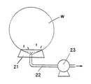
本発明の水置換法を用いず、基板表面に水分を残す乾燥法の例としては、吸引乾燥法がある。
図8に示したように、真空吸引ライン22が設置された乾燥台座21に材料基板Wを垂直に載せ、真空ポンプ23で基板Wの両表面周りに存在するクリーンエアを気流として吸引すると同時に基板Wの両表面上の水滴や水膜を吸引除去して乾燥させる方法である。この方法によれば、材料基板表面上の水分量を必要以上に低減させずに適度な量にすることができるので、接合に要する水分を基板表面上に残して乾燥することができる。また、乾燥台座に複数枚数の基板を載置可能とすることで、同時に多数の基板を乾燥することができるので、生産性の向上を図ることができる。
【0022】
また、本発明の乾燥工程には、いわゆるスピン乾燥機を使用することができる。
図9に示したスピン乾燥機25は、モーター26で高速回転する支持台27を有するもので、支持台27上に材料基板Wを載置し、材料基板W上の水分を、基板Wを水平状態で高速回転することにより発生する遠心力を用いて、材料基板上の水分の除去を行う。この場合も、材料基板の表面上に残す水分量を適度にすることができる。
【0023】
また、本発明では、洗浄工程における最終リンス槽のリンス液を温水とし、最終リンス槽からゆっくりと基板を引き上げることで、材料基板上の温水を蒸発させて材料基板の水分を除去する方法(以下、温水引上げ乾燥法と呼ぶ)を用いることもできる。この時、乾燥を確実にするため、材料基板にIR(赤外線)照射を行っても良い。また、基板を同時に複数枚処理できるので、生産性が高い。この場合も、乾燥基板表面に残留する水分量を適度な量にすることができる。
【0024】
以上述べた本発明によれば、従来の水置換法として用いられているIPA蒸気乾燥法等と比較して、IPA等の引火性の高い薬品を用いないので、安全に操業できると同時に、多額の設備費を必要とする安全対策およびIPA等の薬品のコストが不要になるので、貼り合せ基板の製造コストを引き下げることができる。なお、本発明では、上記乾燥工程を複数回繰り返し行っても良い。
【0025】
本発明は、SOI(Silicon on Insulator)基板、SOQ(Silicon on Quartz)基板、誘電体分離基板、酸化膜を介さずシリコンウエーハ同士を接合した基板、その他接合により作製できるあらゆる貼り合せ基板に適用できる。また、洗浄工程と乾燥工程と接合工程が備わる手法であれば、貼り合せ基板のあらゆる作製手法に限定されずに適用できる。
【0026】
特に、水素注入剥離法による貼り合せ基板の作製では、材料基板内に形成された水素高濃度層で材料基板の剥離を行う。この水素高濃度層の形成にはイオン注入法が用いられるが、基板表面品質を劣化させるため、接合した材料基板を剥離する際の接合界面の接合強度が弱く、接合界面にボイド不良やブリスター不良を発生させ易い欠点がある。しかし、本発明のように基板表面に水分を残す乾燥法を用いることで、接合界面の水素結合を担う水分やOH基が水置換法よりも格段に増加するので、剥離時の接合界面の接合強度が向上し、ボイド不良やブリスター不良が著しく減少し、接合界面品質と生産歩留りが向上する。
【0027】
このように、水置換法ではなく基板表面に水分を残す乾燥法を使用することで、接合基板の接合界面における接合強度が向上すると同時に、材料基板上からパーティクルおよび有機物汚染が低減するので、結合熱処理によって結合強度が増強され、結合界面にボイド不良やブリスター不良の無い高品質貼り合せ基板を高生産性および高歩留りで得ることができる。
【0028】
【発明の実施の形態】
以下、本発明に係わる貼り合せ基板を製造する実施の形態について図面を参照しながら詳細に説明する。
図1は、本発明に係わる貼り合せ基板の製造方法の一実施形態の概要を示す工程図である。ここでは、貼り合せ基板の作製法の一種である水素注入剥離法を用いたSOI基板の作製を例に説明する。
【0029】
図1において、材料基板としてベアウエーハを2枚用意する(A)。ベアウエーハには、鏡面研磨ウエーハ、エピタキシャルウエーハ、熱処理基板等様々な基板が存在するが、その種類に関係なく本発明に適用することができる。
まず、ボンドウエーハ1として用意されたベアウエーハの表面に酸化膜10を形成する。表面に酸化膜10が形成されたボンドウエーハ1の表面から水素イオンの注入を行い、所望の深さに均一に水素高濃度層11を形成する。水素高濃度層11の深さが、得られるSOI層の厚さを決めることになる。
【0030】
次に、ベースウエーハ2としてはベアウエーハをそのまま用いる。ここで、ボンドウエーハ1をベアウエーハとし、ベースウエーハ2を酸化膜付ウエーハとしても良い。また、共にベアウエーハまたは酸化膜付ウエーハとしても良い。
これらの材料基板の表面に付着しているパーティクルおよび有機物等を除去するため、材料基板の接合前に洗浄工程を行う(B)。この洗浄工程ではいわゆるRCA洗浄等の洗浄を行い、その後の乾燥工程(C)では水置換法ではなくウエーハ表面に水分を残す方法を採用して、接合前の材料基板上に水分およびOH基を残すようにして乾燥する。
【0031】
次に、接合工程(D)において、その表面に水分の残っているボンドウエーハ1の表面とベースウエーハ2の表面を接合する。この時、接合工程の雰囲気や材料基板を保管した容器から、パーティクル汚染および有機物汚染を受け易いので、洗浄工程、乾燥工程を行った後は、出来る限り早く接合工程を行うことが望ましい。
【0032】
剥離熱処理工程(E)においては、接合した基板を400〜600℃程度の低温で熱処理すると、ボンドウエーハ1内に形成された水素高濃度層11に欠陥層が形成される。欠陥層がボンドウエーハ1内部で水平方向に繋がることで、ボンドウエーハ1の剥離を行う。これにより、ボンドウエーハ1の一部がベースウエーハ2上に転写して、SOI基板となる。
【0033】
結合熱処理工程(F)においては、接合界面の接合力を高めるため、酸化性雰囲気または非酸化性雰囲気で1000℃以上の結合熱処理を行い、強固に結合させて安定化する。最後に研磨工程(G)において、SOI層表面のダメージを除去し、マイクロラフネスを向上させるための研磨を行う。研磨の代わりに水素アニール等の熱処理を行うこともできる。
以上の一連の工程により水素注入剥離法によるSOIウエーハ15が完成する。
【0034】
図3は、200℃以下で接合した接合基板の接合界面における接合状態を説明する概略図である(参考文献:阿部孝夫著、シリコン結晶成長とウエーハ加工、培風館、1994、p.330)。図3から、接合界面の接合状態は水分およびOH基を主体とした水素結合であることが分かる。従って、接合界面に水分およびOH基が適度に多いときには接合界面の接合強度は向上する。
【0035】
図4は、接合後、200〜700℃で低温熱処理を行った後の、接合基板の接合界面の接合状態を説明する概略図である(参考文献:阿部孝夫著、シリコン結晶成長とウエーハ加工、培風館、1994、p.330)。この場合、接合界面の接合状態は、シラノール基を主体とした接合であることが分かる。しかしながら、熱処理温度を上げるに従って、接合界面の接合は水素結合からシラノール基による結合へ徐々に変化しているので、実際の接合界面の接合は、水素結合とシラノール基結合が混在した状態となっている。従って、接合時において接合界面の水分およびOH基が適度に多いほど、熱処理後の接合強度も向上する。
【0036】
ところで、水素注入剥離法では、材料基板内に1×10¹⁶ions/cm2 以上の水素が存在すれば、400℃以上の温度で微小欠陥層を形成して剥離が起きる。上述したように、400℃以上の温度では、接合界面の結合状態が、シラノール基による結合と水素結合の混在した状態である。そのため、接合時において、材料基板上に適度に多くの水分およびOH基が存在した方が、接合界面の接合強度を向上させ、ボイド不良やブリスター不良を低減させることができる。
【0037】
また、水素注入剥離法では、材料基板への水素の注入量を1×10¹⁷ions/cm2 以上とすれば、材料基板内に発生する微小欠陥層が400℃以下でも形成されるため、水素の注入量が多ければ多いほど、剥離熱処理温度を下げることができ、接合界面の接合は水素結合がより主体となる。そのため、接合界面の接合強度が弱く、ボイド欠陥やブリスター不良が発生し易い。それゆえ接合時に、材料基板上に適度に多くの水分およびOH基を存在させ、接合界面の接合強度を向上させることで、低温で剥離させる場合でもボイド不良やブリスター不良を低減させることができる。水素を励起してプラズマ状態で注入することにより剥離工程を室温で行う技術を用いる場合も同様である。
【0038】
そこで、接合前に行う洗浄工程と乾燥工程を行った後の材料基板上の水分量について、水置換法を用いない吸引乾燥法と水置換法を用いるIPA蒸気乾燥法とで比較を行った。
【0039】
まず、TOF−SIMS法(飛行時間型2次イオン質量分析法)を用いて、基板乾燥後の材料基板上のSiOH基を測定した結果を示す。図5は、基板表面から検出されたSiOHフラグメントの量を示している。乾燥法による違いを比較し易くするため、30Siで規格化している。その結果、水置換法を用いたIPA蒸気乾燥法よりも、水置換法ではない吸引乾燥法の方が、接合界面の接合の担い手となるSiOH基が多いことが分かった。
【0040】
また、図6は、基板表面から検出されたOHフラグメントの量を示している。乾燥法による違いを比較し易くするため、30Siで規格化している。その結果、水置換法を用いたIPA蒸気乾燥法よりも、水置換法ではない吸引乾燥法の方が、接合界面の結合の担い手となるOH基が多いことが分かった。従って、TOF−SIMS法の結果から、吸引乾燥法で乾燥した材料基板の方が、水置換法を用いたIPA蒸気乾燥法よりも、OHおよびSiOH基が多くなることが分かった。
【0041】
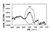
続いて、図7に、ATR−IR(Attenuated Total Reflection Infrared)スペクトル法(以下、ATR−IR法と呼ぶ)を用いて、基板乾燥後の材料基板上の水分およびSiOH基を測定した結果を示す。結果は波形で表されるが、乾燥法による違いを比較し易くするため、吸引乾燥法の波形から、IPA蒸気乾燥法の波形を引いた波形で表している。その結果、水分を示す1800cm-1付近のピークが正側に振れ、IPA蒸気乾燥法よりも、吸引乾燥法の方が、水分が多くなる傾向が見られた。ゆえに、ATR−IR法の結果からは、水置換法ではない吸引乾燥法で乾燥した材料基板の方が、水置換法を用いたIPA蒸気乾燥法よりも、水分が多くなることが分かった。
【0042】
【実施例】
以下、本発明の実施例と比較例を挙げて本発明を具体的に説明するが、本発明はこれらに限定されるものではない。
(実施例)
接合前の洗浄工程後の乾燥工程で行う乾燥法の違いによる材料基板上の水分量の違いが、接合基板の接合界面の接合強度にどの程度の差となって現れるかを剃刀法を用いて調査した(剃刀法についての参考文献:編集UCS半導体基板技術研究会、SOIの科学、リアライズ社、2000年、p.300)。
【0043】
ここでは、貼り合せ基板の作製法の一種である水素注入剥離法を用いてSOI基板を作製した。製造工程は図1に示された工程図による。
先ず、150nm酸化膜付直径8インチシリコン基板に8×10¹⁶ions/cm2 の水素イオンを注入したボンドウエーハと、ベアシリコン基板をベースウエーハとして用意した。
次に、両ウエーハをRCA洗浄液で洗浄した後、純水で十分リンスした。続いて吸引乾燥法を用いて両ウエーハを乾燥した。次いで、ボンドウエーハの酸化膜面とベースウエーハの片面とを室温で接合した。そして、接合した基板に水素高濃度層が剥離しない300℃で熱処理を行った後、接合界面の接合強度を剃刀法により測定したところ、0.28〜0.33N/m2 であった。
【0044】
次に、上記したように、接合強度を測定したウエーハと同じ履歴のウエーハを用いて、水素注入剥離法による貼り合せ基板の作製を行ない、500℃、30分の剥離熱処理工程後における貼り合せ基板の良品率を調査した。
ここで、剥離熱処理工程後における貼り合せ基板の良品とは、剥離熱処理工程後に得られる貼り合せ基板表面上に、図2に示すようなボイド不良あるいはブリスター不良が、蛍光灯下の目視検査で観察されない基板のことである。また剥離熱処理工程後における貼り合せ基板の良品率とは、剥離熱処理工程後における貼り合せ基板の良品の枚数を、投入枚数で割り、100倍したものである。
上記のように、吸引乾燥法により乾燥して貼り合せ基板を16枚作製したところ、15枚の良品を得ることができた(良品率:94%)。
【0045】
さらに、モニター基板を用いて、接合前の洗浄工程後の乾燥工程を行った材料基板上のパーティクル数をKLA−Tencor社製パーティクルカウンタ−SP1で測定したところ、吸引乾燥法では、0.2μm以上のパーティクルが〜5個/直径8インチウエーハしか検出されなかった。
【0046】
(比較例)
接合前の洗浄工程後の乾燥工程に、水置換法であるIPA蒸気乾燥法を用いた以外は実施例と同様の工程で水素注入剥離法によるSOIウエーハを作製して比較例とした。
そして、実施例と同様に剃刀法により、接合基板の接合界面の接合強度を測定したところ、0.18〜0.22N/m2 であった。
また、500℃、30分の剥離熱処理を行った貼り合せ基板を16枚作製したところ、7枚の良品しか得られなかった(良品率:44%)。
さらに、モニター基板を用いてパーティクル数を測定したところ、接合前のIPA蒸気乾燥した材料基板上には0.2μm以上のパーティクルが〜10個/直径8インチウエーハ検出された。
【0047】
以上述べた実施例と比較例の結果から、水置換法を用いない吸引乾燥法(実施例)を使用した方が、材料基板上に水分およびOH基が適度に残留するので、接合界面の接合強度が向上することが分かる。
【0048】
また、水置換法のIPA蒸気乾燥を行うと、乾燥後の材料基板表面が静電気で帯電し、乾燥工程の基板回収場所あるいは基板保管箱あるは接合工程の雰囲気に存在するパーティクルが付着し易くなるものと考えられる。
【0049】
このように、水置換法を用いない吸引乾燥法を用いることで、材料基板上に水分またはOH基が適度に多く存在するため、水置換法のIPA蒸気乾燥では接合界面の接合強度が弱い剥離工程においても、接合界面の接合強度を向上させることができる。また、静電気が発生しないので、材料基板上のパーティクル汚染が低減する。さらに、IPA等の有機溶剤を使用しないため、有機物汚染も低減させることができる。このため、接合界面の品質が向上し、結合熱処理後の貼り合せ基板の製品歩留りが向上する。
【0050】
なお、本発明は、上記実施形態では水置換法であるIPA蒸気乾燥法を使用しないことを前提としているが、一旦IPA蒸気乾燥を行った後、再度純水のみで基板を濡らし、水置換法ではなく、基板上に水分を残す本乾燥法を用いることで、接合基板の接合界面の接合強度を、IPA蒸気乾燥のみの場合の0.18〜0.22N/m2 から、0.25〜0.31N/m2 まで高めることができた。従って、IPA蒸気乾燥後に、純水のみで基板を濡らし、本乾燥法を実施して基板上に水分を残すようにすることによっても、接合界面の接合強度を向上させることができることがわかった。
【0051】
さらに、剥離工程後の良品率を調査したところ、比較例におけるIPA蒸気乾燥したサンプルでは、投入枚数16枚に対し、7枚の良品しか得られなかった(良品率:44%)が、このようにIPA蒸気乾燥後に再度基板を濡らしてから吸引乾燥法を行うことで、投入枚数16枚に対し、12枚の良品を得ることが出来た(良品率:75%)。
ここで、本実験は、IPA蒸気乾燥法で乾燥した基板を、再度、純水で濡らしただけで吸引乾燥法を行っているが、メガソニックあるいはブラシを併用したり、薬液を用いたりすることで、接合強度の向上以外に、パーティクルや有機物汚染も低減させるようにすることができる。このため、本発明では、IPA蒸気乾燥後に、本乾燥法である吸引乾燥法、スピン乾燥法、温水引上げ乾燥法等を使用することもできる。
【0052】
なお、本発明は、上記実施形態に限定されるものではない。上記実施形態は、例示であり、本発明の特許請求の範囲に記載された技術的思想と実質的に同一な構成を有し、同様な作用効果を奏するものは、いかなるものであっても本発明の技術的範囲に包含される。
【0053】
例えば、材料基板として半導体基板以外に、石英基板等の絶縁性基板または金属基板等にも適用することができる。また、デバイス等のパターン付基板にも適用することができる。
さらに、上記実施形態において、水素注入剥離法における剥離工程を熱処理で行っているが、熱処理に相当するエネルギー(電気、プラズマ、高周波等)を与えても良い。
また、熱処理および熱処理に相当するエネルギーを与えて、水素高濃度層に微小欠陥層を形成し、基板側面から微小欠陥層に流体(気体、液体)を噴射して、ボンドウエーハを剥離しても良い。
【0054】
また、貼り合せ基板の作製方法に関しても、上記水素注入剥離法に限定されるものではなく、2枚の基板を結合した後、一方の基板をエッチング、研削、研磨あるいは気相エッチング等により薄膜化、平坦化するような方法においても、本発明が適用できることは言うまでもない。
【0055】
【発明の効果】
接合前の洗浄工程後の乾燥工程において、水置換法を用いない乾燥法を用いて接合前の材料基板上に水分を残すことにより、接合後の接合界面の接合強度を格段に高めることができる。また材料基板が静電気で帯電しなくなるので、0.2μm以上のサイズのパーティクルによる汚染が低減する。さらに有機溶剤を使用しないため、有機物汚染も低減する。従って、貼り合せ基板の結合界面からボイド不良やブリスター不良が低減し、貼り合せ基板の生産歩留りが著しく向上する。さらに、水置換法のように薬品を使用しないため、安全に操業できると共に、薬品代および安全対策のための設備が不要となり、製造コストを引き下げることができる。
【図面の簡単な説明】
【図1】本発明に係る貼り合せ基板製造の一実施形態を示す工程図である。
【図2】貼り合せ基板のブリスター不良およびボイド不良を示す説明図である。
【図3】材料基板を200℃以下で接合した場合の接合基板の接合界面の接合状態を表す説明図である。
【図4】材料基板を接合後、200〜700℃で熱処理を行った後の、接合基板の接合界面の接合状態を示す説明図である。
【図5】TOF−SIMS法を用いて、基板乾燥後の材料基板上のSiOH基の量を乾燥法で比較した図である。
【図6】TOF−SIMS法を用いて、基板乾燥後の材料基板上のOHの量を比較した図である。
【図7】ATR−IR法を用いて、基板乾燥後の材料基板上の水分を乾燥法で比較した図である。
【図8】吸引乾燥法を示す説明図である。
【図9】スピン乾燥法を示す説明図である。
【符号の説明】
1…ボンドウエーハ、 2…ベースウエーハ、
9…シリコン、 10…酸化膜、 11…水素高濃度層、
12…ブリスター不良、 13…ボイド不良、 15…SOIウエーハ、
21…台座、 22…真空吸引ライン、 23…真空ポンプ、
25…スピン乾燥機、 26…モーター、 27…支持台、
W…基板(ウエーハ)。[0001]
BACKGROUND OF THE INVENTION
The present invention relates to a cleaning process and a drying process before bonding a substrate as a material in manufacturing a bonded substrate.
[0002]
[Prior art]
In the manufacture of a bonded substrate, the substrates that are single or plural kinds of materials are washed and dried, and then the material substrates are bonded. Thereafter, heat treatment is performed to increase the bonding strength at the bonding interface of the bonded substrates and the substrates are firmly bonded, and then one substrate is thinned to produce a bonded substrate. Here, the drying process performed after the cleaning process of the material substrate is usually performed by placing the substrate in a heated vapor of IPA (isopropyl alcohol), which is a kind of highly volatile organic solvent, and condensing the substrate on the surface of the substrate. This is performed by a water replacement method typified by a method (hereinafter referred to as an IPA vapor drying method) in which the substrate is heated to a vapor temperature and dried while replacing adhering moisture.
[0003]
In the production of a bonded substrate, when particles and organic substances are present on the bonding surface of the material substrate when bonding the material substrates, the particles and organic substances hinder the bonding at the bonding interface and form unbonded portions at the bonding interface. This causes void defects and blister defects at the bonding interface of the bonded substrate after the bonding heat treatment. In particular, when the bonding force at the bonding interface is weak, void defects and blister defects are likely to occur even when bonding heat treatment is performed, and the size tends to increase.
[0004]
FIG. 2 is a diagram schematically showing a longitudinal section of an SOI wafer as an example of a bonded substrate in which these defects have occurred.
In an SOI wafer, an
[0005]
In the production of a bonded substrate that has been conventionally performed, a water replacement method such as the above-described IPA vapor drying method is used in a drying step performed after a material substrate cleaning step. When a bonded substrate is manufactured using a substrate dried by this water replacement method, the void defect and blister defect are likely to occur, and the productivity and yield of the bonded substrate are reduced.
[0006]
Here, the water replacement method is a method of quickly drying the substrate by replacing the water adhering to the substrate surface with a highly volatile organic solvent. As a replacement solvent, IPA, which is most easily used industrially, is widely used.
[0007]
Furthermore, since the IPA vapor drying method may cause a fire, a large amount of capital investment was required for its safety measures. Moreover, since IPA is a high-purity chemical, it is expensive and its use increases the manufacturing cost.
[0008]
[Problems to be solved by the invention]
Therefore, the present invention has been made in view of such conventional problems, and by performing a cleaning process before bonding the material substrate and optimizing the subsequent drying process, the bonding strength of the bonding interface of the bonding substrate is achieved. The main object is to provide a method for manufacturing a bonded substrate that can manufacture a bonded substrate free from void defects or blister defects at the bonding interface of the bonded substrate after bonding heat treatment with high productivity and yield. And
[0009]
[Means for Solving the Problems]
In order to solve the above-described problems, the invention according to the method for manufacturing a bonded substrate of the present invention includes a step of bonding at least two substrates and a step of firmly bonding the bonded substrates by applying heat treatment. In the substrate manufacturing method, at least before the substrates are bonded, a cleaning process is performed to remove contaminants on the substrate surface, and then the cleaned substrate surface is dried. In the drying process, a water replacement method is used. It is characterized by not increasing the bonding strength after bonding substrates by leaving moisture on the substrates before bonding..
[0010]
Thus, before bonding the substrates, perform a cleaning process to remove contaminants on the substrate surface, then perform a process of drying the cleaned substrate surface, and in the drying process, without using a water displacement method, If the substrate is bonded by leaving moisture on the substrate surface before bonding, the bonding strength can be strongly increased by hydrogen bonding, silanol group bonding, or the like. If this bonded substrate is bonded by bonding heat treatment, a bonded substrate having a strong bonding strength at the bonding interface can be manufactured, and particles and organic contamination on the substrate as a material can be reduced. A high-quality bonded substrate free from void defects or blister defects at the subsequent bonding interface can be manufactured with high productivity and high yield.
[0011]
In this case, the bonding strength at the bonding interface after bonding is 0.25 N / m.2Preferably above.
Thus, according to the present invention, the bonding strength at the bonding interface after bonding can be easily increased to 0.25 N / m.2Therefore, the bonding interface strength of the bonded substrate after the bonding heat treatment can be increased to a higher strength than the conventional one. Further, if it is above this value, for example, it is higher than the peel strength of the microbubble layer at the time of peeling in the hydrogen injection peeling method, so that no void defect or blister defect occurs at the bonding interface.
[0012]
In this case, the drying process can be a process of sucking and removing moisture on the cleaned substrate surface..
This step is a step of removing moisture on the surface of the material substrate by placing the material substrate almost vertically on a drying pedestal provided with a vacuum suction line and sucking moisture from the lower portion of the substrate. By mounting a plurality of substrates on the drying base, a plurality of substrates can be dried at the same time, so that high productivity can be obtained. In addition, the amount of moisture remaining on the substrate surface used in the bonding process can be made moderate.
[0013]
In this case, the drying step can be a step of removing moisture on the cleaned substrate surface by rotating the substrate at a high speed..
In this step, moisture on the material substrate is removed using a centrifugal force obtained by rotating the substrate at a high speed, and a normal spin dryer corresponds to this process. Also in the case of a spin dryer, the amount of moisture remaining on the substrate surface can be made moderate.
[0014]
Further, in this case, the cleaning step is a step of performing a final rinse with warm water, and the next drying step can be a step of evaporating and removing the warm water on the cleaned substrate surface..
As described above, the rinse liquid in the final rinse tank in the cleaning step is used as warm water, and the substrate is slowly pulled up from the final rinse tank, whereby the warm water on the material substrate surface can be evaporated and the moisture in the material substrate can be removed. In this case, IR irradiation may be performed on the material substrate in order to ensure drying..Further, since a plurality of substrates can be processed simultaneously, productivity is high. Furthermore, it is possible to moderate the amount of moisture remaining on the substrate surface.
[0015]
Here, in the invention according to the method for manufacturing a bonded substrate of the present invention, it is preferable that the substrate used as the material of the bonded substrate is a silicon substrate.,It is also preferable to use a silicon substrate with an oxide film.,Alternatively, hydrogen, a rare gas, or a halogen gas can be injected..
[0016]
As described above, a substrate used as a material for a bonded substrate is used by combining a plurality of types of substrates depending on the type of device and application. Among them, a silicon substrate, a silicon substrate with an oxide film, or hydrogen, a rare gas, or a halogen is used. If a bonded substrate is manufactured by applying a cleaning process and a drying process of the present invention using a gas-injected silicon substrate, strong bonding strength and strong bonding strength can be obtained, and there is no contamination or defect. A bonded substrate can be provided.
[0017]
Furthermore, according to the present invention, the material substrate, which is manufactured by the above-described manufacturing method and is free from particles and organic contamination, is strongly bonded by moisture, further increases the bonding interface strength by bonding heat treatment, and voids or blister defects at the bonding interface. A bonded substrate without any problem is provided.
[0018]
Hereinafter, the present invention will be described in detail.
The inventors of the present invention have proposed that the bonding strength obtained in the bonding step of the bonded substrate is, for example, a microbubble layer (ion implantation) when performing separation in a hydrogen implantation separation method (sometimes referred to as an ion implantation separation method or a smart cut method). In some cases, it is weaker than the peeling strength of the high-concentration layer and the hydrogen high-concentration layer. The present invention has been completed by finding a drying method and drying conditions capable of avoiding this phenomenon, and by examining various conditions and finding out that the method tends to be weak when using the method.
[0019]
That is, according to this water replacement method, moisture and OH groups on the substrate surface are almost completely volatilized, so that moisture and OH groups responsible for hydrogen bonding are insufficient at the bonding interface of the bonded substrate, and bonding at the bonding interface is performed. It has been found that the strength is decreasing.
In addition, static electricity is charged on the substrate surface after drying, and particles having a size of 0.2 μm or more tend to adhere to the substrate surface. Furthermore, since IPA itself is an organic solvent, the surface of the material substrate was contaminated with organic substances.
[0020]
Therefore, in the present invention, as a drying method in the drying process performed after the cleaning process for cleaning the material substrate, a water substitution method such as an IPA vapor drying method is not used. By leaving the OH group, bonding mainly including hydrogen bonding occurs and the bonding strength at the bonding interface is improved. Further, since the residual moisture can prevent the material substrate from being charged by static electricity, adhesion of particles having a size of 0.2 μm or more on the material substrate surface can be reduced. Furthermore, since the present drying method that does not use the water replacement method does not use an organic solvent such as IPA, it does not cause organic contamination on the material substrate surface after drying.
For the reasons described above, when the present invention is used, the bonding strength at the bonding interface of the bonding substrate is remarkably improved. Therefore, the bonding strength of the bonded substrate after the bonding heat treatment is enhanced, and the product yield can be improved.
In the present invention, “bonding strength” is a general term for the bonding strength at the bonding interface before the bonding heat treatment at a high temperature of 1000 ° C. or higher, and is distinguished from the “bonding strength” after the bonding heat treatment. .
[0021]
An example of a drying method that leaves water on the substrate surface without using the water replacement method of the present invention is a suction drying method.
As shown in FIG. 8, the material substrate W is placed vertically on the drying
[0022]
Moreover, what is called a spin dryer can be used for the drying process of this invention.
The
[0023]
Further, in the present invention, the rinsing liquid in the final rinsing tank in the cleaning process is used as warm water, and the substrate is slowly pulled up from the final rinsing tank, thereby evaporating the hot water on the material substrate and removing the moisture from the material substrate (hereinafter referred to as the following) Also called hot water pulling drying method). At this time, in order to ensure drying, the material substrate may be irradiated with IR (infrared rays). In addition, since a plurality of substrates can be processed simultaneously, productivity is high. In this case as well, the amount of water remaining on the dry substrate surface can be made moderate.
[0024]
According to the present invention described above, compared with the IPA vapor drying method used as a conventional water replacement method, it does not use highly flammable chemicals such as IPA, so it can be operated safely and at the same time This eliminates the need for safety measures and the cost of chemicals such as IPA, which can reduce the manufacturing cost of the bonded substrate. In the present invention, the drying step may be repeated a plurality of times.
[0025]
The present invention can be applied to an SOI (Silicon on Insulator) substrate, an SOQ (Silicon on Quartz) substrate, a dielectric isolation substrate, a substrate in which silicon wafers are bonded without using an oxide film, and any other bonded substrate that can be manufactured by bonding. . In addition, any technique including a cleaning process, a drying process, and a bonding process can be applied without being limited to any manufacturing technique of a bonded substrate.
[0026]
In particular, when a bonded substrate is manufactured by a hydrogen implantation separation method, the material substrate is peeled off with a hydrogen high-concentration layer formed in the material substrate. An ion implantation method is used to form this high-concentration hydrogen layer. However, since the surface quality of the substrate is degraded, the bonding strength at the bonding interface when the bonded material substrate is peeled off is weak, and void defects or blister defects are formed at the bonding interface. There is a drawback that it is easy to generate. However, by using a drying method that leaves moisture on the substrate surface as in the present invention, the water and OH groups responsible for hydrogen bonding at the bonding interface are significantly increased compared to the water replacement method. Strength is improved, void defects and blister defects are remarkably reduced, and bonding interface quality and production yield are improved.
[0027]
In this way, using a drying method that leaves moisture on the substrate surface instead of a water replacement method improves the bonding strength at the bonding interface of the bonded substrate, and at the same time reduces particle and organic contamination from the material substrate. The bonding strength is enhanced by the heat treatment, and a high-quality bonded substrate free from void defects or blister defects at the bonding interface can be obtained with high productivity and high yield.
[0028]
DETAILED DESCRIPTION OF THE INVENTION
DESCRIPTION OF EMBODIMENTS Hereinafter, embodiments for producing a bonded substrate according to the present invention will be described in detail with reference to the drawings.
FIG. 1 is a process diagram showing an outline of an embodiment of a method for producing a bonded substrate according to the present invention. Here, an example of manufacturing an SOI substrate using a hydrogen implantation separation method, which is a kind of manufacturing method of a bonded substrate, will be described.
[0029]
In FIG. 1, two bare wafers are prepared as material substrates (A). There are various substrates such as mirror-polished wafers, epitaxial wafers, heat-treated substrates, and the like, which can be applied to the present invention regardless of their types.
First, the
[0030]
Next, a bare wafer is used as it is as the
In order to remove particles and organic substances adhering to the surface of these material substrates, a cleaning process is performed before joining the material substrates (B). In this cleaning step, so-called RCA cleaning or the like is performed, and in the subsequent drying step (C), a method of leaving moisture on the wafer surface instead of the water replacement method is adopted, so that moisture and OH groups are formed on the material substrate before bonding. Leave to dry.
[0031]
Next, in the bonding step (D), the surface of the
[0032]
In the peeling heat treatment step (E), when the bonded substrates are heat treated at a low temperature of about 400 to 600 ° C., a defect layer is formed in the hydrogen
[0033]
In the bonding heat treatment step (F), in order to increase the bonding force at the bonding interface, bonding heat treatment at 1000 ° C. or higher is performed in an oxidizing atmosphere or a non-oxidizing atmosphere to firmly bond and stabilize. Finally, in the polishing step (G), polishing for removing damage on the surface of the SOI layer and improving microroughness is performed. Instead of polishing, heat treatment such as hydrogen annealing can be performed.
Through the series of steps described above, the
[0034]
3 is a schematic diagram for explaining the bonding state at the bonding interface of the bonded substrates bonded at 200 ° C. or lower (reference: Takao Abe, silicon crystal growth and wafer processing, Baifukan, 1994, p. 330). From FIG. 3, it can be seen that the bonding state at the bonding interface is hydrogen bonds mainly composed of moisture and OH groups. Accordingly, the bonding strength at the bonding interface is improved when the bonding interface has a moderate amount of moisture and OH groups.
[0035]
FIG. 4 is a schematic diagram for explaining the bonding state of the bonding interface of the bonded substrate after performing low-temperature heat treatment at 200 to 700 ° C. after bonding (reference: written by Takao Abe, silicon crystal growth and wafer processing, Baifukan, 1994, p.330). In this case, it can be seen that the bonding state at the bonding interface is bonding mainly composed of silanol groups. However, as the heat treatment temperature is raised, the bonding at the bonding interface gradually changes from hydrogen bonding to bonding with silanol groups, so the bonding at the actual bonding interface becomes a state in which hydrogen bonding and silanol group bonding are mixed. Yes. Therefore, the bonding strength after the heat treatment is improved as the amount of moisture and OH groups at the bonding interface is appropriately increased during bonding.
[0036]
By the way, in the hydrogen implantation separation method, 1 × 10 10 is formed in the material substrate.16ions / cm2 If the above hydrogen exists, peeling occurs by forming a micro defect layer at a temperature of 400 ° C. or higher. As described above, at a temperature of 400 ° C. or higher, the bonding state at the bonding interface is a state in which bonding by silanol groups and hydrogen bonding are mixed. For this reason, when a moderate amount of moisture and OH groups are present on the material substrate at the time of bonding, the bonding strength at the bonding interface can be improved, and void defects and blister defects can be reduced.
[0037]
In the hydrogen injection separation method, the amount of hydrogen injected into the material substrate is set to 1 × 10.17ions / cm2 With the above, a minute defect layer generated in the material substrate is formed even at 400 ° C. or lower. Therefore, the greater the amount of hydrogen injected, the lower the heat treatment temperature for peeling, and the bonding at the bonding interface is hydrogen bonding. Becomes more subject. Therefore, the bonding strength at the bonding interface is weak, and void defects and blister defects are likely to occur. Therefore, at the time of bonding, a reasonably large amount of moisture and OH groups are present on the material substrate and the bonding strength at the bonding interface is improved, so that void defects and blister defects can be reduced even when peeling is performed at a low temperature. The same applies to the case of using a technique in which the exfoliation process is performed at room temperature by injecting hydrogen in a plasma state.
[0038]
Therefore, the water content on the material substrate after performing the cleaning process and the drying process before bonding was compared between the suction drying method that does not use the water replacement method and the IPA vapor drying method that uses the water replacement method.
[0039]
First, the result of having measured the SiOH group on the material board | substrate after drying a board | substrate using TOF-SIMS method (time-of-flight type secondary ion mass spectrometry) is shown. FIG. 5 shows the amount of SiOH fragments detected from the substrate surface. In order to make it easy to compare the differences between the drying methods, it is standardized with 30Si. As a result, it was found that the suction drying method that is not the water replacement method has more SiOH groups that are responsible for bonding at the bonding interface than the IPA vapor drying method that uses the water replacement method.
[0040]
FIG. 6 shows the amount of OH fragments detected from the substrate surface. In order to make it easy to compare the differences between the drying methods, it is standardized with 30Si. As a result, it was found that the suction drying method that is not the water replacement method has more OH groups that are responsible for bonding at the bonding interface than the IPA vapor drying method that uses the water replacement method. Therefore, from the result of the TOF-SIMS method, it was found that the material substrate dried by the suction drying method has more OH and SiOH groups than the IPA vapor drying method using the water displacement method.
[0041]
Subsequently, FIG. 7 shows a result of measuring moisture and SiOH groups on the material substrate after drying the substrate using an ATR-IR (Attenuated Total Reflection Infrared) spectrum method (hereinafter referred to as ATR-IR method). . Although the result is represented by a waveform, in order to make it easier to compare the differences due to the drying method, the waveform is represented by subtracting the waveform of the IPA vapor drying method from the waveform of the suction drying method. As a result, 1800cm showing moisture-1The peak in the vicinity sways to the positive side, and there was a tendency for the moisture to be increased in the suction drying method than in the IPA vapor drying method. Therefore, from the results of the ATR-IR method, it was found that the material substrate dried by the suction drying method which is not the water displacement method has more water than the IPA vapor drying method using the water displacement method.
[0042]
【Example】
EXAMPLES Hereinafter, although an Example and comparative example of this invention are given and this invention is demonstrated concretely, this invention is not limited to these.
(Example)
Using the razor method, the difference in the amount of moisture on the material substrate due to the difference in the drying method performed in the drying process after the cleaning process before bonding appears as a difference in the bonding strength at the bonding interface of the bonding substrate. (Reference literature on the razor method: Editorial UCS Semiconductor Substrate Technology Research Group, SOI Science, Realize, 2000, p. 300).
[0043]
Here, an SOI substrate was manufactured using a hydrogen implantation separation method which is a kind of a method for manufacturing a bonded substrate. The manufacturing process is based on the process diagram shown in FIG.
First, 8 × 10 on an 8-inch silicon substrate with a 150 nm oxide film.16ions / cm2 A bond wafer into which hydrogen ions were implanted and a bare silicon substrate were prepared as a base wafer.
Next, both wafers were washed with an RCA cleaning solution and then rinsed thoroughly with pure water. Subsequently, both wafers were dried using a suction drying method. Next, the oxide film surface of the bond wafer and one surface of the base wafer were bonded at room temperature. And after performing heat processing at 300 degreeC which a hydrogen high concentration layer does not peel to the board | substrate joined, when the joint strength of the joining interface was measured with the razor method, 0.28-0.33 N / m2 Met.
[0044]
Next, as described above, using the wafer having the same history as the wafer whose bonding strength was measured, a bonded substrate was prepared by the hydrogen injection separation method, and the bonded substrate after the separation heat treatment step at 500 ° C. for 30 minutes. The percentage of good products was investigated.
Here, the non-defective product of the bonded substrate after the exfoliation heat treatment process is observed by visual inspection under a fluorescent lamp on the surface of the bonded substrate obtained after the exfoliation heat treatment step as shown in FIG. A substrate that is not. Further, the non-defective product ratio of the bonded substrate after the peeling heat treatment step is obtained by dividing the number of non-defective products of the bonded substrate after the peeling heat treatment step by 100 and multiplying by 100.
As described above, when 16 bonded substrates were produced by drying by the suction drying method, 15 good products could be obtained (good product rate: 94%).
[0045]
Furthermore, when the number of particles on the material substrate subjected to the drying process after the cleaning process before bonding was measured using a monitor substrate with a particle counter-SP1 manufactured by KLA-Tencor, 0.2 μm or more was obtained in the suction drying method. Only 5 particles / 8 inch diameter wafers were detected.
[0046]
(Comparative example)
An SOI wafer by a hydrogen injection delamination method was prepared as a comparative example in the same process as the example except that the IPA vapor drying method which is a water displacement method was used for the drying step after the cleaning step before bonding.
And when the joint strength of the joint interface of a joining board | substrate was measured by the razor method similarly to the Example, it was 0.18-0.22 N / m.2 Met.
Further, when 16 bonded substrates subjected to a peeling heat treatment at 500 ° C. for 30 minutes were produced, only 7 good products were obtained (good product rate: 44%).
Furthermore, when the number of particles was measured using a monitor substrate, 10 particles / 8 inch diameter wafer were detected on the material substrate dried by IPA vapor drying before bonding.
[0047]
From the results of the examples and comparative examples described above, the use of the suction drying method (examples) that does not use the water displacement method allows moisture and OH groups to remain on the material substrate appropriately. It can be seen that the strength is improved.
[0048]
In addition, when IPA vapor drying is performed by water substitution, the material substrate surface after drying is electrostatically charged, and particles present in the substrate recovery place of the drying process, the substrate storage box, or the atmosphere of the bonding process are likely to adhere. It is considered a thing.
[0049]
In this way, by using the suction drying method that does not use the water displacement method, there is a reasonably large amount of moisture or OH groups on the material substrate. Also in the process, the bonding strength at the bonding interface can be improved. In addition, since static electricity is not generated, particle contamination on the material substrate is reduced. Furthermore, since no organic solvent such as IPA is used, organic contamination can be reduced. For this reason, the quality of the bonding interface is improved, and the product yield of the bonded substrate after the bonding heat treatment is improved.
[0050]
Note that the present invention is based on the premise that the IPA vapor drying method, which is a water replacement method, is not used in the above embodiment, but after the IPA vapor drying is performed once, the substrate is again wetted with pure water only, and the water replacement method is performed. Instead, by using this drying method that leaves moisture on the substrate, the bonding strength at the bonding interface of the bonding substrate is 0.18 to 0.22 N / m in the case of only IPA vapor drying.2 To 0.25 to 0.31 N / m2 I was able to increase it. Therefore, it has been found that the bonding strength at the bonding interface can be improved also by wetting the substrate with pure water only after IPA vapor drying and performing this drying method to leave moisture on the substrate.
[0051]
Further, when the rate of non-defective products after the peeling process was investigated, in the IPA vapor-dried sample in the comparative example, only 7 non-defective products were obtained with respect to the input number of 16 sheets (non-defective product rate: 44%). In addition, by performing the suction drying method after wetting the substrate again after IPA vapor drying, it was possible to obtain 12 non-defective products with respect to the input number of 16 sheets (non-defective product rate: 75%).
Here, in this experiment, the substrate dried by the IPA vapor drying method is subjected to the suction drying method just by re-wetting it with pure water. However, using a megasonic or brush together, or using a chemical solution Thus, in addition to improving the bonding strength, it is possible to reduce particle and organic contamination. Therefore, in the present invention, after the IPA vapor drying, a suction drying method, a spin drying method, a hot water pulling drying method, or the like, which is a main drying method, can be used.
[0052]
The present invention is not limited to the above embodiment. The above-described embodiment is an exemplification, and the present invention has the same configuration as the technical idea described in the claims of the present invention. It is included in the technical scope of the invention.
[0053]
For example, the present invention can be applied to an insulating substrate such as a quartz substrate or a metal substrate in addition to a semiconductor substrate as a material substrate. It can also be applied to a substrate with a pattern such as a device.
Furthermore, in the above embodiment, the peeling step in the hydrogen implantation peeling method is performed by heat treatment, but energy (electricity, plasma, high frequency, etc.) corresponding to the heat treatment may be applied.
Also, heat treatment and energy equivalent to heat treatment are applied to form a microdefect layer in the hydrogen high-concentration layer, and fluid (gas, liquid) is sprayed from the side surface of the substrate to the microdefect layer to peel off the bond wafer. good.
[0054]
Also, the method for manufacturing a bonded substrate is not limited to the above hydrogen implantation separation method, and after bonding two substrates, one substrate is thinned by etching, grinding, polishing, vapor phase etching, or the like. Needless to say, the present invention can be applied to a flattening method.
[0055]
【The invention's effect】
In the drying process after the cleaning process before bonding, the bonding strength at the bonding interface after bonding can be significantly increased by leaving moisture on the material substrate before bonding using a drying method that does not use the water replacement method. . Further, since the material substrate is not charged by static electricity, contamination by particles having a size of 0.2 μm or more is reduced. Further, since no organic solvent is used, organic contamination is also reduced. Therefore, void defects and blister defects are reduced from the bonding interface of the bonded substrate, and the production yield of the bonded substrate is significantly improved. Furthermore, since no chemicals are used unlike the water replacement method, it is possible to operate safely, and equipment for chemical costs and safety measures are not required, and manufacturing costs can be reduced.
[Brief description of the drawings]
FIG. 1 is a process diagram showing an embodiment of manufacturing a bonded substrate according to the present invention.
FIG. 2 is an explanatory diagram showing blister defects and void defects of a bonded substrate;
FIG. 3 is an explanatory diagram showing the bonding state of the bonding interface of the bonded substrate when the material substrates are bonded at 200 ° C. or lower.
FIG. 4 is an explanatory diagram illustrating a bonding state of a bonding interface of a bonded substrate after performing heat treatment at 200 to 700 ° C. after bonding the material substrates.
FIG. 5 is a diagram comparing the amount of SiOH groups on a material substrate after drying using the TOF-SIMS method by a drying method.
FIG. 6 is a diagram comparing the amount of OH on a material substrate after drying the substrate using the TOF-SIMS method.
FIG. 7 is a diagram comparing moisture on a material substrate after drying a substrate by a drying method using an ATR-IR method.
FIG. 8 is an explanatory view showing a suction drying method.
FIG. 9 is an explanatory diagram showing a spin drying method.
[Explanation of symbols]
1 ... bond wafer, 2 ... base wafer,
9 ... Silicon, 10 ... Oxide film, 11 ... Hydrogen high concentration layer,
12 ... Blister failure, 13 ... Void failure, 15 ... SOI wafer,
21 ... pedestal, 22 ... vacuum suction line, 23 ... vacuum pump,
25 ... Spin dryer, 26 ... Motor, 27 ... Support stand,
W: Substrate (wafer).
Claims (4)
Priority Applications (7)
| Application Number | Priority Date | Filing Date | Title |
|---|---|---|---|
| JP2001119457A JP4628580B2 (en) | 2001-04-18 | 2001-04-18 | Manufacturing method of bonded substrate |
| KR1020097009265A KR20090064476A (en) | 2001-04-18 | 2002-04-09 | Production method for bonded substrates |
| CNB028012755A CN1271721C (en) | 2001-04-18 | 2002-04-09 | Production method for bonded substrates |
| KR1020027017000A KR20030008163A (en) | 2001-04-18 | 2002-04-09 | Production method for bonded substrates |
| EP02714551A EP1381086A4 (en) | 2001-04-18 | 2002-04-09 | Production method for bonded substrates |
| US10/311,438 US6959854B2 (en) | 2001-04-18 | 2002-04-09 | Production method for bonded substrates |
| PCT/JP2002/003522 WO2002086975A1 (en) | 2001-04-18 | 2002-04-09 | Production method for bonded substrates |
Applications Claiming Priority (1)
| Application Number | Priority Date | Filing Date | Title |
|---|---|---|---|
| JP2001119457A JP4628580B2 (en) | 2001-04-18 | 2001-04-18 | Manufacturing method of bonded substrate |
Publications (2)
| Publication Number | Publication Date |
|---|---|
| JP2002313689A JP2002313689A (en) | 2002-10-25 |
| JP4628580B2 true JP4628580B2 (en) | 2011-02-09 |
Family
ID=18969673
Family Applications (1)
| Application Number | Title | Priority Date | Filing Date |
|---|---|---|---|
| JP2001119457A Expired - Lifetime JP4628580B2 (en) | 2001-04-18 | 2001-04-18 | Manufacturing method of bonded substrate |
Country Status (6)
| Country | Link |
|---|---|
| US (1) | US6959854B2 (en) |
| EP (1) | EP1381086A4 (en) |
| JP (1) | JP4628580B2 (en) |
| KR (2) | KR20090064476A (en) |
| CN (1) | CN1271721C (en) |
| WO (1) | WO2002086975A1 (en) |
Families Citing this family (34)
| Publication number | Priority date | Publication date | Assignee | Title |
|---|---|---|---|---|
| JP2003204048A (en) * | 2002-01-09 | 2003-07-18 | Shin Etsu Handotai Co Ltd | Method for manufacturing soi wafer and soi wafer |
| FR2842646B1 (en) * | 2002-07-17 | 2005-06-24 | Soitec Silicon On Insulator | METHOD OF INCREASING THE AREA OF A USEFUL LAYER OF MATERIAL REFLECTED ON A SUPPORT |
| US7084078B2 (en) * | 2002-08-29 | 2006-08-01 | Micron Technology, Inc. | Atomic layer deposited lanthanide doped TiOx dielectric films |
| US7235461B2 (en) * | 2003-04-29 | 2007-06-26 | S.O.I.Tec Silicon On Insulator Technologies | Method for bonding semiconductor structures together |
| FR2854493B1 (en) * | 2003-04-29 | 2005-08-19 | Soitec Silicon On Insulator | SCRUBBING TREATMENT OF SEMICONDUCTOR PLATE BEFORE COLLAGE |
| FR2855908B1 (en) * | 2003-06-06 | 2005-08-26 | Soitec Silicon On Insulator | METHOD FOR OBTAINING A STRUCTURE COMPRISING AT LEAST ONE SUBSTRATE AND AN ULTRAMINO LAYER |
| FR2860340B1 (en) * | 2003-09-30 | 2006-01-27 | Soitec Silicon On Insulator | INDIRECT BONDING WITH DISAPPEARANCE OF THE BONDING LAYER |
| JPWO2005045908A1 (en) * | 2003-11-06 | 2007-05-24 | 松下電器産業株式会社 | Substrate bonding method, bonded substrate and direct bonding substrate |
| US7650688B2 (en) * | 2003-12-31 | 2010-01-26 | Chippac, Inc. | Bonding tool for mounting semiconductor chips |
| JP2006080314A (en) | 2004-09-09 | 2006-03-23 | Canon Inc | Manufacturing method of coupled substrate |
| CN101027769B (en) * | 2004-09-21 | 2017-06-23 | Soitec公司 | Transfer method with the treatment to wanting bonding surface |
| JP2006303089A (en) * | 2005-04-19 | 2006-11-02 | Sumco Corp | Cleaning method of silicon substrate |
| US20070023850A1 (en) * | 2005-07-30 | 2007-02-01 | Chien-Hua Chen | Bonding surfaces together via plasma treatment on both surfaces with wet treatment on only one surface |
| JP2007141946A (en) * | 2005-11-15 | 2007-06-07 | Sumco Corp | Method of manufacturing soi substrate, and soi substrate manufactured by same |
| JP5168788B2 (en) * | 2006-01-23 | 2013-03-27 | 信越半導体株式会社 | Manufacturing method of SOI wafer |
| JP5315596B2 (en) * | 2006-07-24 | 2013-10-16 | 株式会社Sumco | Manufacturing method of bonded SOI wafer |
| US7981754B2 (en) | 2006-09-07 | 2011-07-19 | Renesas Electronics Corporation | Manufacturing method of bonded SOI substrate and manufacturing method of semiconductor device |
| JP2008153411A (en) * | 2006-12-18 | 2008-07-03 | Shin Etsu Chem Co Ltd | Manufacturing method of soi substrate |
| FR2912839B1 (en) * | 2007-02-16 | 2009-05-15 | Soitec Silicon On Insulator | IMPROVING THE QUALITY OF COLD CLEANING INTERFACE BY COLD CLEANING AND HOT COLLAGE |
| TWI492275B (en) | 2008-04-10 | 2015-07-11 | Shinetsu Chemical Co | The method of manufacturing the bonded substrate |
| JP5760392B2 (en) * | 2009-11-04 | 2015-08-12 | ボンドテック株式会社 | Bonding method, bonding system, and semiconductor device |
| US9299556B2 (en) | 2010-12-27 | 2016-03-29 | Shanghai Simgui Technology Co. Ltd. | Method for preparing semiconductor substrate with insulating buried layer gettering process |
| CN102130038A (en) * | 2010-12-27 | 2011-07-20 | 上海新傲科技股份有限公司 | Method for preparing silicon-on-insulator by ion implantation |
| CN102130039B (en) * | 2010-12-27 | 2013-04-10 | 上海新傲科技股份有限公司 | Method for preparing semiconductor substrate with insulated buried layer by adopting gettering process |
| JP2011193010A (en) * | 2011-04-28 | 2011-09-29 | Hitachi Cable Ltd | Semiconductor wafer and semiconductor wafer for high frequency electronic device |
| JP5580251B2 (en) * | 2011-06-13 | 2014-08-27 | 株式会社日立ハイテクマニファクチャ&サービス | Wafer bonding strength inspection apparatus and method |
| FR2981941B1 (en) | 2011-10-26 | 2014-06-06 | Commissariat Energie Atomique | METHOD FOR DIRECTLY TREATING AND BONDING A LAYER OF MATERIAL |
| WO2014021192A1 (en) * | 2012-07-30 | 2014-02-06 | 芝浦メカトロニクス株式会社 | Substrate bonding apparatus and substrate bonding method |
| US9434145B2 (en) | 2012-12-07 | 2016-09-06 | Semrock, Inc. | Dichroic filter conformed to optical surface |
| JP5630527B2 (en) * | 2013-04-12 | 2014-11-26 | 株式会社Sumco | Manufacturing method of bonded SOI wafer |
| JP6558355B2 (en) | 2016-12-19 | 2019-08-14 | 信越半導体株式会社 | Manufacturing method of SOI wafer |
| CN109103079B (en) * | 2018-08-06 | 2021-06-01 | 济南晶正电子科技有限公司 | Nanoscale single crystal film and preparation method thereof |
| CN109727904B (en) * | 2018-12-28 | 2020-08-21 | 安徽龙芯微科技有限公司 | Film coating device for wafer |
| US20210066547A1 (en) | 2019-08-28 | 2021-03-04 | Tslc Corporation | Semiconductor Components And Semiconductor Structures And Methods Of Fabrication |
Citations (8)
| Publication number | Priority date | Publication date | Assignee | Title |
|---|---|---|---|---|
| JPH0397215A (en) * | 1989-09-11 | 1991-04-23 | Toshiba Corp | Manufacture of semiconductor wafer |
| JPH0758303A (en) * | 1993-08-20 | 1995-03-03 | Shin Etsu Handotai Co Ltd | Manufacture of coupling type substate |
| JPH09186127A (en) * | 1995-12-28 | 1997-07-15 | Shiii & I:Kk | Semiconductor wafer cleaning and drying method and apparatus |
| JPH1050657A (en) * | 1996-08-06 | 1998-02-20 | Shin Etsu Handotai Co Ltd | Method and apparatus for drying platelike material |
| JPH10209111A (en) * | 1997-01-24 | 1998-08-07 | Hitachi Ltd | Method and equipment for manufacturing semiconductor device |
| JPH11307507A (en) * | 1998-04-21 | 1999-11-05 | Super Silicon Kenkyusho:Kk | Wafer drying device |
| JP2000030992A (en) * | 1998-07-10 | 2000-01-28 | Shin Etsu Handotai Co Ltd | Manufacture of bonded wafer and bonded water |
| WO2001093334A1 (en) * | 2000-05-30 | 2001-12-06 | Shin-Etsu Handotai Co.,Ltd. | Method for producing bonded wafer and bonded wafer |
Family Cites Families (10)
| Publication number | Priority date | Publication date | Assignee | Title |
|---|---|---|---|---|
| US4052524A (en) * | 1975-08-15 | 1977-10-04 | Monsanto Company | Method for improving adhesive bonding in steel/rubber composites and article |
| US5451547A (en) * | 1991-08-26 | 1995-09-19 | Nippondenso Co., Ltd. | Method of manufacturing semiconductor substrate |
| JP2701709B2 (en) * | 1993-02-16 | 1998-01-21 | 株式会社デンソー | Method and apparatus for directly joining two materials |
| US6033764A (en) * | 1994-12-16 | 2000-03-07 | Zecal Corp. | Bumped substrate assembly |
| JPH09331049A (en) * | 1996-04-08 | 1997-12-22 | Canon Inc | Pasted soi substrate and its production |
| US5858144A (en) * | 1996-04-12 | 1999-01-12 | Iowa State University Research Foundation, Inc. | Low temperature joining of ceramic composites |
| US6270202B1 (en) * | 1997-04-24 | 2001-08-07 | Matsushita Electric Industrial Co., Ltd. | Liquid jetting apparatus having a piezoelectric drive element directly bonded to a casing |
| WO1999010927A1 (en) * | 1997-08-29 | 1999-03-04 | Farrens Sharon N | In situ plasma wafer bonding method |
| US6410436B2 (en) * | 1999-03-26 | 2002-06-25 | Canon Kabushiki Kaisha | Method of cleaning porous body, and process for producing porous body, non-porous film or bonded substrate |
| JP2003535807A (en) * | 2000-06-20 | 2003-12-02 | ショット、グラス、テクノロジーズ、インコーポレイテッド | Glass ceramic composite |
-
2001
- 2001-04-18 JP JP2001119457A patent/JP4628580B2/en not_active Expired - Lifetime
-
2002
- 2002-04-09 US US10/311,438 patent/US6959854B2/en not_active Expired - Lifetime
- 2002-04-09 KR KR1020097009265A patent/KR20090064476A/en active Search and Examination
- 2002-04-09 EP EP02714551A patent/EP1381086A4/en not_active Withdrawn
- 2002-04-09 KR KR1020027017000A patent/KR20030008163A/en not_active Application Discontinuation
- 2002-04-09 CN CNB028012755A patent/CN1271721C/en not_active Expired - Lifetime
- 2002-04-09 WO PCT/JP2002/003522 patent/WO2002086975A1/en active Application Filing
Patent Citations (8)
| Publication number | Priority date | Publication date | Assignee | Title |
|---|---|---|---|---|
| JPH0397215A (en) * | 1989-09-11 | 1991-04-23 | Toshiba Corp | Manufacture of semiconductor wafer |
| JPH0758303A (en) * | 1993-08-20 | 1995-03-03 | Shin Etsu Handotai Co Ltd | Manufacture of coupling type substate |
| JPH09186127A (en) * | 1995-12-28 | 1997-07-15 | Shiii & I:Kk | Semiconductor wafer cleaning and drying method and apparatus |
| JPH1050657A (en) * | 1996-08-06 | 1998-02-20 | Shin Etsu Handotai Co Ltd | Method and apparatus for drying platelike material |
| JPH10209111A (en) * | 1997-01-24 | 1998-08-07 | Hitachi Ltd | Method and equipment for manufacturing semiconductor device |
| JPH11307507A (en) * | 1998-04-21 | 1999-11-05 | Super Silicon Kenkyusho:Kk | Wafer drying device |
| JP2000030992A (en) * | 1998-07-10 | 2000-01-28 | Shin Etsu Handotai Co Ltd | Manufacture of bonded wafer and bonded water |
| WO2001093334A1 (en) * | 2000-05-30 | 2001-12-06 | Shin-Etsu Handotai Co.,Ltd. | Method for producing bonded wafer and bonded wafer |
Also Published As
| Publication number | Publication date |
|---|---|
| KR20090064476A (en) | 2009-06-18 |
| CN1271721C (en) | 2006-08-23 |
| EP1381086A1 (en) | 2004-01-14 |
| US20040035525A1 (en) | 2004-02-26 |
| CN1461496A (en) | 2003-12-10 |
| KR20030008163A (en) | 2003-01-24 |
| JP2002313689A (en) | 2002-10-25 |
| US6959854B2 (en) | 2005-11-01 |
| EP1381086A4 (en) | 2009-12-16 |
| WO2002086975A1 (en) | 2002-10-31 |
Similar Documents
| Publication | Publication Date | Title |
|---|---|---|
| JP4628580B2 (en) | Manufacturing method of bonded substrate | |
| JP3385972B2 (en) | Manufacturing method of bonded wafer and bonded wafer | |
| US8202785B2 (en) | Surface treatment for molecular bonding | |
| US7645682B2 (en) | Bonding interface quality by cold cleaning and hot bonding | |
| KR100936778B1 (en) | Wafer bonding Method | |
| JP2008021971A (en) | Method of directly bonding two substrates used for electronics, optics, or optoelectronics | |
| JP3900741B2 (en) | Manufacturing method of SOI wafer | |
| TWI492275B (en) | The method of manufacturing the bonded substrate | |
| KR101541940B1 (en) | Method for producing soi substrate | |
| JP2006210899A (en) | Process for producing soi wafer, and soi wafer | |
| JP2010538459A (en) | Reuse of semiconductor wafers in delamination processes using heat treatment | |
| WO2001093334A1 (en) | Method for producing bonded wafer and bonded wafer | |
| KR100827907B1 (en) | Process for cleaning silicon substrate | |
| US20060148208A1 (en) | Method for producing a silicon-on-insulator structure | |
| JP5320954B2 (en) | Manufacturing method of SOI wafer | |
| JP6643873B2 (en) | Method of laminating two substrates | |
| JP4016701B2 (en) | Manufacturing method of bonded substrate | |
| JP2006216662A (en) | Process for producing bonding soi wafer, and the bonding soi wafer | |
| US7439189B2 (en) | Surface treatment after selective etching | |
| JP3611142B2 (en) | Bonded wafer and manufacturing method thereof | |
| JP2004128389A (en) | Manufacturing method of laminated soi wafer | |
| KR102568640B1 (en) | Method for producing the remainder of the donor substrate, substrate produced by the method and use of the substrate | |
| WO2015056386A1 (en) | Bonded wafer manufacturing method | |
| JP2000315635A (en) | Silicon wafer for bonding and manufacture of bonded substrate using the same | |
| JP2000315634A (en) | Silicon wafer for bonding and manufacture of bonded substrate |
Legal Events
| Date | Code | Title | Description |
|---|---|---|---|
| A131 | Notification of reasons for refusal |
Free format text: JAPANESE INTERMEDIATE CODE: A131 Effective date: 20070710 |
|
| A521 | Request for written amendment filed |
Free format text: JAPANESE INTERMEDIATE CODE: A523 Effective date: 20070823 |
|
| A02 | Decision of refusal |
Free format text: JAPANESE INTERMEDIATE CODE: A02 Effective date: 20080122 |
|
| A521 | Request for written amendment filed |
Free format text: JAPANESE INTERMEDIATE CODE: A523 Effective date: 20080319 |
|
| A521 | Request for written amendment filed |
Free format text: JAPANESE INTERMEDIATE CODE: A523 Effective date: 20080519 |
|
| A911 | Transfer to examiner for re-examination before appeal (zenchi) |
Free format text: JAPANESE INTERMEDIATE CODE: A911 Effective date: 20080527 |
|
| A912 | Re-examination (zenchi) completed and case transferred to appeal board |
Free format text: JAPANESE INTERMEDIATE CODE: A912 Effective date: 20080620 |
|
| A521 | Request for written amendment filed |
Free format text: JAPANESE INTERMEDIATE CODE: A523 Effective date: 20100922 |
|
| A01 | Written decision to grant a patent or to grant a registration (utility model) |
Free format text: JAPANESE INTERMEDIATE CODE: A01 |
|
| A61 | First payment of annual fees (during grant procedure) |
Free format text: JAPANESE INTERMEDIATE CODE: A61 Effective date: 20101110 |
|
| FPAY | Renewal fee payment (event date is renewal date of database) |
Free format text: PAYMENT UNTIL: 20131119 Year of fee payment: 3 |
|
| R150 | Certificate of patent or registration of utility model |
Ref document number: 4628580 Country of ref document: JP Free format text: JAPANESE INTERMEDIATE CODE: R150 Free format text: JAPANESE INTERMEDIATE CODE: R150 |
|
| R250 | Receipt of annual fees |
Free format text: JAPANESE INTERMEDIATE CODE: R250 |
|
| R250 | Receipt of annual fees |
Free format text: JAPANESE INTERMEDIATE CODE: R250 |
|
| R250 | Receipt of annual fees |
Free format text: JAPANESE INTERMEDIATE CODE: R250 |
|
| S531 | Written request for registration of change of domicile |
Free format text: JAPANESE INTERMEDIATE CODE: R313531 |
|
| R350 | Written notification of registration of transfer |
Free format text: JAPANESE INTERMEDIATE CODE: R350 |
|
| R250 | Receipt of annual fees |
Free format text: JAPANESE INTERMEDIATE CODE: R250 |
|
| R250 | Receipt of annual fees |
Free format text: JAPANESE INTERMEDIATE CODE: R250 |
|
| R250 | Receipt of annual fees |
Free format text: JAPANESE INTERMEDIATE CODE: R250 |
|
| R250 | Receipt of annual fees |
Free format text: JAPANESE INTERMEDIATE CODE: R250 |
|
| R250 | Receipt of annual fees |
Free format text: JAPANESE INTERMEDIATE CODE: R250 |
|
| EXPY | Cancellation because of completion of term |