JP4625623B2 - Optical disk playback device - Google Patents
Optical disk playback device Download PDFInfo
- Publication number
- JP4625623B2 JP4625623B2 JP2003379292A JP2003379292A JP4625623B2 JP 4625623 B2 JP4625623 B2 JP 4625623B2 JP 2003379292 A JP2003379292 A JP 2003379292A JP 2003379292 A JP2003379292 A JP 2003379292A JP 4625623 B2 JP4625623 B2 JP 4625623B2
- Authority
- JP
- Japan
- Prior art keywords
- signal
- defect
- reproduction signal
- flaw
- offset
- Prior art date
- Legal status (The legal status is an assumption and is not a legal conclusion. Google has not performed a legal analysis and makes no representation as to the accuracy of the status listed.)
- Expired - Fee Related
Links
Images


Description
本発明は、光ディスクから信号を再生する装置に関し、特に傷、ブラックドット、指紋等が付着した光ディスクであっても、高速な信号再生が可能な装置に関する。 The present invention relates to an apparatus for reproducing a signal from an optical disk, and more particularly to an apparatus capable of reproducing a signal at high speed even with an optical disk having scratches, black dots, fingerprints, and the like attached thereto.
従来の光ディスク再生装置では、光ディスクに記録された情報の再生信号(RF信号)を、自動調整されたスライスレベルで2値化し、次段のデジタル処理回路に2値化信号を渡していた。例えば、信号スライスレベルよりもRF信号の値が大きいときは「1」、小さいときは「0」と判定する2値化方式が提案されている(特許文献1参照)。 In a conventional optical disk reproducing apparatus, a reproduction signal (RF signal) of information recorded on an optical disk is binarized at an automatically adjusted slice level, and the binarized signal is passed to the next digital processing circuit. For example, a binarization method has been proposed in which “1” is determined when the value of the RF signal is larger than the signal slice level and “0” is determined when the value is smaller (see Patent Document 1).
これに対して、多ビットのデジタル信号に標本化し、パーシャルレスポンス方式と最尤復号方式(マキシマムライクリフッド)の一つであるビタビ復号器を組み合わせたPRML(Partial Response Maximum Likelihood)信号方式が提案されている。このPRML信号方式は、線記録方向の記録密度の増加に伴い、意図的に波形干渉を付加することにより、高域成分を必要としない再生系を実現し、波形干渉を考慮した確率計算により、再生データの品質を向上させる方式である(特許文献2参照)。 On the other hand, a partial response maximum likelihood (PRML) signal method that combines a Viterbi decoder, which is one of the partial response method and the maximum likelihood decoding method (sampled into a multi-bit digital signal), is proposed. Has been. This PRML signal system realizes a playback system that does not require high frequency components by intentionally adding waveform interference as the recording density in the linear recording direction increases, and by probability calculation considering waveform interference, This is a method for improving the quality of reproduced data (see Patent Document 2).
図3はDVD-RAM規格に基づく光ディスクのフォーマットを示すものである。ここに示すように、DVD-RAMディスクは、アドレス情報を格納するヘッダー部と、ユーザデータを格納する情報記録部(データ部)で構成される。ヘッダー部においてアドレス情報は、ID1〜ID4に格納されており、ID1,2とID3,4はデータトラックに対し各々1/2トラックだけ内周側または外周側にずらして設けられている。データ部は、グルーブトラックとランドトラックから構成され、両者が交互に設けられている(非特許文献1参照)。 FIG. 3 shows an optical disc format based on the DVD-RAM standard. As shown here, the DVD-RAM disc is composed of a header section for storing address information and an information recording section (data section) for storing user data. In the header portion, address information is stored in ID1 to ID4, and ID1, 2 and ID3, 4 are shifted from the data track by ½ track each on the inner or outer periphery side. The data part is composed of a groove track and a land track, and both are provided alternately (see Non-Patent Document 1).
まず、正常なデータ再生を説明する。DVD-RAMにおいて、ヘッダ部に格納されたアドレス情報とデータ部に記録されたユーザデータの再生方法について、図2を用い説明する。 First, normal data reproduction will be described. A method of reproducing address information stored in the header portion and user data recorded in the data portion in the DVD-RAM will be described with reference to FIG.
図2(a)は、アイディーゲート(IDGATE)であり、Highの区間はヘッダ部の期間を示し、Lowの区間はデータ部の期間を示す。 FIG. 2A shows an ID gate, where a high section indicates a header section period and a low section indicates a data section period.
図2(b)は、リードゲート(RDGATE)であり、RF信号の中心レベルをリファレンス電位に一致させるための制御信号であるとともに、再生クロック(RCLK)を生成するPLL回路において、同期信号を切り替える制御信号である。具体的には、RDGATEがHighのとき、再生クロックはRF信号の2値化信号に同期され、RDGATEがLowのとき、再生クロックはウォブルクロック(Wobble CK)に同期される。なお、ウォブルクロックは、あらかじめディスクに記録されているウォブル(図3参照)を再生することで、Wobble PLL部で生成される。 FIG. 2B shows a read gate (RDGATE), which is a control signal for matching the center level of the RF signal to the reference potential, and switches the synchronization signal in the PLL circuit that generates the reproduction clock (RCLK). Control signal. Specifically, when RDGATE is High, the recovered clock is synchronized with the binary signal of the RF signal, and when RDGATE is Low, the recovered clock is synchronized with the wobble clock (Wobble CK). The wobble clock is generated by the Wobble PLL unit by reproducing the wobble (see FIG. 3) recorded in advance on the disc.
RDGATEがHighのときには、低周波のDC変動を排除したり、再生信号を生成するPLL部の擬似ロック防止のため、ハイパスフィルタ(HPF)のカットオフ周波数を低くする。ここでは、カットオフ周波数を約1kHz程度に設定し、HPF後であっても再生データ情報が十分得るようにしてある。これにより、擬似ロックが生じた場合であっても、HPFがあると、誤った周波数に一旦ロックしても、擬似ロックが続かないという効果がある。なお、擬似ロックとは、再生信号が有するクロック成分の周波数と、PLLにより生成されるクロックの周波数が大きく異なっているときに、PLLにより生成されるクロックが誤った周波数にロックすることである。一方、RDGATEがLowのときには、HPFのカットオフ周波数が高くなるように動作させる。 When RDGATE is High, the cut-off frequency of the high-pass filter (HPF) is lowered to eliminate low-frequency DC fluctuations and to prevent false lock of the PLL unit that generates the reproduction signal. Here, the cut-off frequency is set to about 1 kHz so that sufficient reproduction data information can be obtained even after HPF. As a result, even if a pseudo lock occurs, if there is an HPF, there is an effect that the pseudo lock does not continue even if it is locked to a wrong frequency. The pseudo lock means that the clock generated by the PLL locks to an incorrect frequency when the frequency of the clock component included in the reproduction signal and the frequency of the clock generated by the PLL are greatly different. On the other hand, when RDGATE is low, the operation is performed so that the cutoff frequency of HPF is high.
DVD-RAM規格では、同期を取りやすくしたり、トラッキングエラー信号をとりやすくするため、ヘッダ部の反射率を、データ部の反射率よりも高く設定している。このため、図2(c)に示すように、ヘッダ部の一部とデータ部のRF再生信号にDCレベルの差がある。なお、図2(c)において、RF信号の振幅を示す。 In the DVD-RAM standard, the reflectivity of the header portion is set to be higher than the reflectivity of the data portion in order to facilitate synchronization and to easily obtain a tracking error signal. For this reason, as shown in FIG. 2C, there is a difference in DC level between the RF reproduction signal of a part of the header part and the data part. In FIG. 2C, the amplitude of the RF signal is shown.
ヘッダ部に含まれるアドレスデータを認識するためには、データ部と同じDCレベルに調整してから、所定のスライスレベルにより、再生信号を2値化する必要がある。DCレベルの変動を少なくするため、ヘッダ部ではカットオフ周波数が高いハイパスフィルタを通過させる必要がある。 In order to recognize the address data included in the header portion, it is necessary to binarize the reproduction signal at a predetermined slice level after adjusting to the same DC level as the data portion. In order to reduce the fluctuation of the DC level, it is necessary to pass through a high-pass filter having a high cutoff frequency in the header portion.
図2(d)は、HPF後の再生信号である。網掛けの部分は、1または0の2値を示す。HPFは微分特性を持つため、RF信号の立ち上がりで大きく変化するが、HPFのカットオフ周波数が高いために急速に整定でき、ヘッダ部とデータ部のDCレベルを調整することができる。 FIG. 2D shows a reproduction signal after HPF. The shaded portion indicates a binary value of 1 or 0. Since HPF has a differential characteristic, it changes greatly at the rising edge of the RF signal. However, since the HPF has a high cutoff frequency, it can be quickly settled, and the DC level of the header and data parts can be adjusted.
ヘッダ部とデータ部の間では、HPFによる大きなDC変動が必ず発生するため、再生クロックは、RDGATEがLowの時はWobbleで同期をとる構成をとっている。ID1,ID2とID3,ID4とは、別な位置に書かれたアドレス(図3参照)のため、この間でもWobbleで同期を取る。 Since a large DC fluctuation due to HPF always occurs between the header part and the data part, the recovered clock is configured to be synchronized with Wobble when RDGATE is Low. Since ID1, ID2 and ID3, ID4 are addresses written in different positions (see FIG. 3), they are also synchronized by Wobble.
次に図2(e)〜(h)を用いて、データ先頭(VFO)で傷などの欠陥があるときに、データ再生不能となる理由について説明する。図2(e)は、RDGATEがLowからHighに切り替わる位置に微小な傷があるときのRF信号である。RF信号は、傷のため反射率が低いほうに大きく変動する。 Next, the reason why the data cannot be reproduced when there is a defect such as a scratch at the top of the data (VFO) will be described with reference to FIGS. FIG. 2 (e) shows an RF signal when there is a minute flaw at the position where RDGATE switches from Low to High. The RF signal fluctuates greatly to the lower reflectivity due to scratches.
図2(f)は、(e)をHPFに通した後の再生信号である。HPFの時定数が小さい場合には傷の位置において急激に信号が変動した後に、HPFの時定数が大に切り替わるため、再生信号が所定のDCレベルには直ぐには戻れず、この間、最適なスライスレベルにより2値化することが困難となる。 FIG. 2 (f) shows a reproduction signal after passing (e) through the HPF. When the HPF time constant is small, the signal changes rapidly at the position of the flaw, and then the HPF time constant switches to a large value, so the playback signal does not return immediately to the specified DC level. It becomes difficult to binarize depending on the level.
すなわち、特許文献1に示されるような、傷の検出後にスライスレベルを変化させるフィードバック処理では、HPF切り替え箇所に傷などがある場合、傷検出部で傷を検出しても、再生信号のDCレベルの変動にスライスレベルを追従させることが困難であり、アドレスとデータを適切に2値化できないという問題がある。
That is, in the feedback processing for changing the slice level after detection of a flaw as shown in
図2(g)(h)は、傷有りのときのRF信号(反転)とHPF後の再生信号の実際の波形である。HPFの時定数を小から大に変化にさせる位置での傷は、時定数が小さい場合急峻にDC変動が振られた後に、整定する前に時定数が大となり徐々にDCが下降する特性となる。 FIGS. 2G and 2H are actual waveforms of the RF signal (inverted) when there is a flaw and the reproduction signal after HPF. A scratch at a position where the time constant of the HPF is changed from small to large is characterized by the fact that when the time constant is small, the DC constant fluctuates and then the time constant becomes large and the DC gradually decreases before settling. Become.
フィードバック制御とは、検出した系の出力を入力側に戻し、目標値との偏差に応じて制御動作を起こす制御であり、応答性が良くないという性質が再生信号中に傷などに起因する微小欠陥がある場合に大きな問題となる。このため、制御結果の検出を待たずに、目標値の変動や外乱に応じて制御動作をするフィードフォワード制御が好ましい。 Feedback control is a control that returns the detected system output to the input side and causes a control action in accordance with the deviation from the target value. The characteristic that the response is not good is a small amount caused by scratches in the playback signal. It becomes a big problem when there is a defect. For this reason, feedforward control is preferred in which the control operation is performed in response to fluctuations or disturbances in the target value without waiting for detection of the control result.
すなわち、特許文献1に示される2値化方式では、記録密度が大幅に向上した情報記録媒体を再生する場合には、記録再生系の周波数特性から符号間の干渉が生じ、エラーレートが劣化し、スライスレベルを帰還回路で生成するため、高速処理に対応する事が困難という問題がある。
That is, in the binarization method disclosed in
以上のように、特許文献1の光ディスク装置の構成では、傷、ブラックドット、指紋等の汚れが光ディスクに付着している場合に、スライスレベルが大きく変動し、その収束に時間がかかり、再生時のエラー発生量が増加するという問題がある。
As described above, in the configuration of the optical disc apparatus of
本発明は、再生速度を高速化した場合、汚れ、傷等の欠陥が情報記録媒体にある場合でも、再生信号の復帰が早く、正常再生ができる光ディスク装置を提供するものである。 The present invention provides an optical disc apparatus capable of fast reproduction of a reproduction signal and normal reproduction even when an information recording medium has a defect such as dirt or scratches when the reproduction speed is increased.
上記課題は、アドレス情報が記録されたヘッダ領域と、ユーザ情報の記録が可能なデータ領域と、を備えた光ディスクに対し情報を記録再生する光ディスク装置であって、前記光ディスクから再生した再生信号の欠陥を検出する第1の欠陥検出手段と、該再生信号を再生クロックに基づいて標本化し標本化再生信号を得るアナログデジタル変換手段と、該標本化再生信号の欠陥を検出する第2の欠陥検出手段と、前記第1または第2の欠陥検出手段で判断された、欠陥種類、欠陥位置の情報から、欠陥処理方法を選択する処理方法選択手段と、前記標本化再生信号のオフセットを補正するオフセット補正手段と、を具備しており、該オフセット補正手段は、前記標本化再生信号を積分する機能と、前記標本化再生信号から積分値を減算することによりオフセットを補正する機能と、積分速度を可変する機能と、を有し、前記処理方法選択手段の選択により、前記オフセット補正手段の積分速度を可変する光ディスク装置により改善される。 An object of the present invention is to provide an optical disc apparatus for recording / reproducing information on / from an optical disc having a header area in which address information is recorded and a data area in which user information can be recorded. First defect detection means for detecting a defect, analog-to-digital conversion means for sampling the reproduction signal based on a reproduction clock to obtain a sample reproduction signal, and second defect detection for detecting a defect in the sample reproduction signal Means, processing method selection means for selecting a defect processing method from information on the defect type and defect position determined by the first or second defect detection means, and an offset for correcting the offset of the sampling reproduction signal Correction means, and the offset correction means integrates the sampled reproduction signal and subtracts the integration value from the sampled reproduction signal. Has a function of correcting an offset, and a function of varying the integration rate, by, by selection of the processing method selecting means, it is improved by the optical disc device for varying the integration speed of the offset correction means.
本発明の実施により、傷を有する光ディスクからRF再生信号を得た場合であっても、傷に起因する異常再生状態から正常再生状態への復帰を早急に行なうことができる。 By implementing the present invention, even when an RF playback signal is obtained from an optical disc having a scratch, it is possible to quickly return from the abnormal playback state due to the scratch to the normal playback state.
以下、本発明について図面を用いて説明する。図1は本発明の光ディスク装置の一実施形態を示すブロック図である。ここで、1はプリピット部とデータ部が交互に配置されたDVD-RAM等の光ディスク、2はスピンドルモータ、3は光ヘッド(PU)、4はI/V変換器、5はWobble処理部、6はRFデータ処理部、7は第一の傷検出部、8は傷処理方法選択部、9は制御部、10はホスト、11はPLL部、12は復調信号処理部、110はA/D変換器、111はVCO、112はD/A変換器、113は位相比較器、114はオフセット補正部、1140は積分速度調整部、116は第二の傷検出部である。 The present invention will be described below with reference to the drawings. FIG. 1 is a block diagram showing an embodiment of an optical disk apparatus according to the present invention. Here, 1 is an optical disc such as a DVD-RAM in which prepit portions and data portions are alternately arranged, 2 is a spindle motor, 3 is an optical head (PU), 4 is an I / V converter, 5 is a Wobble processing portion, 6 is an RF data processing unit, 7 is a first flaw detection unit, 8 is a flaw processing method selection unit, 9 is a control unit, 10 is a host, 11 is a PLL unit, 12 is a demodulated signal processing unit, and 110 is an A / D A converter, 111 is a VCO, 112 is a D / A converter, 113 is a phase comparator, 114 is an offset correction unit, 1140 is an integral speed adjustment unit, and 116 is a second flaw detection unit.
光ディスク1はスピンドルモータ2に保持されて回転しており、光ヘッド3は、情報の記録または再生を行うレーザ光を発光する半導体レーザと、半導体レーザからの光をディスク面上に光スポットとして形成する光学系と、光ディスク1からの反射光を用いて情報の再生および自動焦点およびトラック追跡などの光点制御を行うための光検出器とから構成され、光ディスク1上に情報の記録を行い、また光ディスク1上の情報の再生を行う。光ディスク装置は、パーソナルコンピュータ、ワークステーション等のホストコンピュータ(以下「ホスト10」と称す)に接続されており、ホスト10からの命令や情報データを、マイコン等から構成される制御部9を通して情報の記録、再生およびシーク動作を実行する。
The
次に再生処理の動作を説明する。ホスト10から、制御部9に対して再生開始指示を行い、光ヘッド3からの信号を受け、I/V変換器4は、電流電圧変換した再生信号を、ウォブル処理部5及びRFデータ処理部6に出力する。
Next, the operation of the reproduction process will be described. The
Wobble信号処理部5では、ディスクの周期的に蛇行している記録案内溝ウォブル(図3参照)に対応したウォブル信号を抽出し、この信号に同期した2値化信号として、ウォブルクロックを出力する。 The wobble signal processing unit 5 extracts a wobble signal corresponding to a wobbling recording guide groove wobble (refer to FIG. 3) that periodically meanders the disk, and outputs a wobble clock as a binary signal synchronized with this signal. .
RFデータ処理部6は、オートゲインコントロール61(AGC)、ハイパスフィルタ62(HPF)、イコライザ63(EQ)等からなる。AGC61は、I/V変換器4からの信号の振幅を一定になるようにゲインコントロールする。HPF62は、再生信号に含まれている低周波のDC変動を無くすために設けられている。DVD-RAMの場合は、ヘッダー部のアドレスを再生するため、ヘッダー部のDC変動を少なくする必要があり、HPFのカットオフ周波数を高く切り替えるカットオフ周波数(Fc)調整部620が設けられている。
The RF data processing unit 6 includes an auto gain control 61 (AGC), a high pass filter 62 (HPF), an equalizer 63 (EQ), and the like. The
EQ回路は、光学特性による高域成分の減衰を補正する。また、PRML方式では、複数ビットへの影響の度合いは、PRクラスにより決められた値に設定され、ビット相互の干渉の度合いが制御される。例えば、PR(1、2、2、1)を使用する場合には、PR(1、2、2、1)の周波数特性に近くなるようにEQの特性を補正する。PR(1、2、2、1)を使い、8−16変調されたDVDデータの場合は、後述するA/Dコンバータにより、サンプリングされた出力は、0、1、3、5、6の5値のみが取りうる値となる。詳細は後述する。 The EQ circuit corrects attenuation of high frequency components due to optical characteristics. In the PRML system, the degree of influence on a plurality of bits is set to a value determined by the PR class, and the degree of interference between bits is controlled. For example, when PR (1, 2, 2, 1) is used, the EQ characteristic is corrected so as to be close to the frequency characteristic of PR (1, 2, 2, 1). In the case of 8-16 modulated DVD data using PR (1, 2, 2, 1), the output sampled by the A / D converter described later is 0, 1, 3, 5, 6 Only the value is a possible value. Details will be described later.
RFデータ処理部で処理された信号は、第一の傷検出部7にてディスクの傷の有無が判別される。例えば、図5のような傷検出を行なう。第一の傷検出部7では、再生信号の振幅がある一定レベルよりも小の場合に、傷があると判断される。傷がある場合には、傷の位置と傷の種類が判別される。ディスク上の傷は、傷の部分だけ光が反射しないため、一定のスレッシュ以下の振幅レベルならば傷と判断される。
From the signal processed by the RF data processing unit, the first
傷の位置検出では、傷がヘッダ部にあるかデータ部にあるかが判別される。また、RF信号処理部6内で使用するHPFの切り替え(ヘッダ/データ切り替わり部)付近の傷かどうかが判別される。再生信号の傷を見つけた場合は、RFデータ処理部6のAGC61回路等でホールド等の処理を行い、次段のA/Dコンバータの標準入力レンジに合わせた信号を出力する。
In flaw position detection, it is determined whether the flaw is in the header portion or the data portion. Further, it is determined whether or not there is a flaw near the switching (header / data switching unit) of the HPF used in the RF signal processing unit 6. When a scratch on the reproduction signal is found, the
傷処理方法選択部8は、第一の傷検出部で検出された傷の位置、種類と、後述する第二の傷検出部の結果により、傷の処理方法を選択する。 The flaw processing method selection unit 8 selects a flaw processing method according to the position and type of the flaw detected by the first flaw detection unit and the result of the second flaw detection unit described later.
PLL回路11は、RFデータ処理部6、傷検出部7を経たRF信号から、アドレスデータ、ユーザデータを再生するための、リードクロック(RCLK)を生成する。
The
再生信号は、PLL内A/D変換器110にて多ビットのデジタル信号に標本化され、復調信号処理部12にて、再生される。復調信号処理部12は、パーシャルレスポンス方式と最尤復号方式(マキシマムライクリフッド)の一つであるビタビ復号器を組み合わせたPRML信号方式で再生される。
The reproduction signal is sampled into a multi-bit digital signal by the A /
PRML信号方式は、標本化された多ビットのデジタル信号値がビタビ復号で意味を持つため、再生クロックの位相と再生信号が有するクロック成分の位相が同期することが重要となる。また、傷やノイズ等の外乱により、PLL回路11のロックがはずれず、安定して再生クロックを出力することが必要である。
In the PRML signal system, since the sampled multi-bit digital signal value is meaningful in Viterbi decoding, it is important that the phase of the recovered clock is synchronized with the phase of the clock component of the recovered signal. In addition, it is necessary to output the reproduction clock stably without the
再生クロックを生成するPLL回路11は、デジタルPLLである。A/D変換器110には、RFデータ処理部6より、第一の傷検出部7を介し、A/D変換器の入力レンジに合わせた信号が入力される。
The
以下に、A/D変換器の入力波形について説明する。8bit入力とした場合に、4T信号を入力したときのA/D変換器の標準出力振幅波形を図4(a)に示す。また、A/D変換器への標準入力を、図4(b)に示す。さらに、図4(c)にPR(1、2、2、1)の応答波形を示す。 The input waveform of the A / D converter will be described below. Fig. 4 (a) shows the standard output amplitude waveform of the A / D converter when a 4T signal is input when 8-bit input is used. The standard input to the A / D converter is shown in FIG. Further, FIG. 4 (c) shows the response waveform of PR (1, 2, 2, 1).
ここで、4T信号とは、ディスクに書かれたビット列が0000111100001111・・・を繰り返す信号をさす。DVD規格で採用される8−16変調方式では、1と1の間の0の最小値は2個に制限される(RLL(2、7))。この信号をPR(1、2、2、1)を通したとき、1111の部分は、下記のように1221が順番に出力され、足された信号となる。すなわち、
01221
001221
0001221
00001221 の和となり、
013565310・・・となる。このように0、1、3、5、6の5値のみが取りうる値となる。復調信号処理部12内のビタビ複合器には、このように等価された信号を入力する必要がある。等価は、RFデータ処理部6のEQ63でも、良いし、復調信号処理部12内で行なっても良い。
Here, the 4T signal refers to a signal in which a bit string written on the disk repeats 0000111100001111. In the 8-16 modulation method adopted in the DVD standard, the minimum value of 0 between 1 and 1 is limited to 2 (RLL (2, 7)). When this signal is passed through PR (1, 2, 2, 1), the portion 1111 is output in the order of 1221 as shown below. That is,
01221
001221
0001221
00001221 sum,
013556510... Thus, only the five
A/D変換器の中心入力DC値はVdc、入力レンジはVmin(最小DC値)からVmax(最大DC値)である。Vmin〜Vmaxの差をVinとする。A/Dへの標準入力は、(Vin/2)とする。図4(a)に、図4(b)のVdc、Vmin、Vmaxに対応したA/D変換器出力の数値を示す。 The center input DC value of the A / D converter is Vdc, and the input range is from Vmin (minimum DC value) to Vmax (maximum DC value). The difference between Vmin and Vmax is Vin. The standard input to A / D is (Vin / 2). FIG. 4A shows the numerical values of the A / D converter output corresponding to Vdc, Vmin, and Vmax in FIG.
図6(a)にRF信号とRDGATE及びA/D入力信号を示す。ディスクに傷がないときの信号である。図6(b)にディスクに傷があるときのRF信号と第一の傷検出器による傷検出信号及びA/D入力信号を示す。A/D標準入力振幅を、RFデータ処理部6において、A/Dの入力レンジの1/2で出力することにより、この範囲外で振幅が極端に小さい期間が続く場合は、傷と判断することができる。また、一定期間(+)のみ、または(−)期間が続く場合も、傷と判断することができる。 FIG. 6A shows the RF signal, RDGATE, and A / D input signal. This is the signal when the disc is not damaged. FIG. 6B shows an RF signal, a flaw detection signal by the first flaw detector, and an A / D input signal when the disc has a flaw. By outputting the A / D standard input amplitude at 1/2 of the A / D input range in the RF data processing unit 6, if an extremely small period outside the range continues, it is determined as a scratch. be able to. Moreover, it is also possible to determine a scratch when only a certain period (+) or (−) period continues.
図6(b)のRF信号及びA/D入力信号のように、ディスクに傷がついている場合は、極端に反射率が低くなるため、RF信号のDCが急峻に上がる。図6(b)のRF信号の振幅が一定値よりも小さい場合に、第一の傷検出器により傷検出される。 When the disc is scratched like the RF signal and A / D input signal in FIG. 6B, the reflectivity becomes extremely low, so that the DC of the RF signal rises sharply. When the amplitude of the RF signal in FIG. 6B is smaller than a certain value, the first flaw detector detects the flaw.
一方、第一の傷検出部7により、傷と判断されなかった信号であっても、第二の傷検出部116で一定期間一定振幅値以下であれば傷と判断し、PLL11のロックがはずれないようにする。第一の傷検出部では、振幅のみで傷判定を行なっていたが、第二の傷検出部では、A/Dコンバータ出力のDCレベルも重要となる。ゼロ中心に振幅が標準入力されているかどうかを判定する。PLL11では、位相比較器でゼロクロス点の前後の値を使用し、位相誤差を検出する。後段の復調信号処理部12(ビタビ復号回路等)では、DVDの場合、A/Dコンバータによりサンプリングされた5値で所定の計算を行なう。第二の傷検出部は、傷によりこれらの回路に支障がないようにする。
On the other hand, even if the signal is not judged to be a flaw by the first
図6(b)第一の傷検出信号のように、ディスクに傷がある場合には、傷検出の前にチャタリングのような信号が出力されることが多い。このような場合は、PLL11からみれば、ループフィルタを通せば無視できる場合がある。第二の傷検出部116で一定期間一定振幅値以下が続かない為、傷と判断されない。また、チャタリングと同じように、指紋がディスクについている場合、RF信号の振幅変動が続く場合は、傷と判断しない。
When the disc has a flaw as in the first flaw detection signal in FIG. 6B, a signal such as chattering is often output before the flaw detection. In such a case, when viewed from the
また、図6(b)では、第一の傷検出部では、信号振幅のみで判断しているが、傷の前の次第に変化していく箇所もPLL11や復調信号処理部12にとっては、異常信号であるため、傷と判断する。
In FIG. 6 (b), the first flaw detection unit makes a judgment based only on the signal amplitude, but the part that gradually changes before the flaw is also an abnormal signal for the
図6(C)に示すように、傷の後一定時間はA/D入力が大きく振られる。第一の傷検出部により、傷が未検出と判定された場合でも、A/D入力信号は正常な標準入力と比較し、大きくうねっていることがわかる。図では、傷の後150us期間の間オフセットが大きく発生し、その後に正常波形となる。そのため、第二の傷検出器では、次のような処理を行なう。 As shown in FIG. 6C, the A / D input is greatly shaken for a certain time after the wound. It can be seen that the A / D input signal is greatly swelled compared to the normal standard input even when the first scratch detection unit determines that no scratch has been detected. In the figure, a large offset occurs during the 150us period after the wound, and then a normal waveform is obtained. Therefore, the second flaw detector performs the following process.
まず、(+)側または(−)側のみに信号が、一定期間ある場合には、第二の傷検出器では、傷と判断する(ステップ1)。または、徐々に大、または小の傾きがある場合には、傷と判断する。 First, when there is a signal for a certain period only on the (+) side or the (−) side, the second flaw detector determines that it is a flaw (step 1). Alternatively, if there is a gradually large or small inclination, it is determined as a scratch.
次に、(+)(−)の両側に信号がある場合には、オフセット補正部114内積分速度調整部1140により、早く追従するように係数を可変する(ステップ2)。
Next, when there are signals on both sides of (+) and (−), the coefficient is varied so that the integral
これにより、時定数切り替え部の傷による変動が早く整定され、データを正常に再生できる。 Thereby, the fluctuation | variation by the damage | wound of a time constant switching part is settled quickly, and data can be reproduced | regenerated normally.
ループフィルタで落とせないほど長い傷が一定時間続く場合には、第二の傷検出部116で傷と判断されるため、位相比較器113及びオフセット補正部114の出力をホールドまたは0に固定する。PLLのロックがはずれないようにするためである。
If a long scratch that cannot be removed by the loop filter continues for a certain period of time, the second
通常は、第一の検出部で一定期間の長い傷が検出された場合は、RFデータ処理部6にて、A/D入力でこのような大きな振幅変動がないようRFデータ処理部でホールドまたはクランプ等の処理を行う。しかし、RF信号処理部は、フィードバック系の処理が多い為、傷があっても直ぐに追従しない場合がある。そのため、第二の検出器で傷を検出した場合は、ホールドまたは、固定値を出力する等の処理を行い、傷にすばやく反応し、次段回路への影響を少なくする。 Normally, when a long scratch for a certain period is detected by the first detection unit, the RF data processing unit 6 holds or prevents the A / D input from causing such a large amplitude fluctuation. Processing such as clamping. However, since the RF signal processing unit has a lot of feedback processing, it may not immediately follow even if there is a scratch. Therefore, when a flaw is detected by the second detector, a process such as holding or outputting a fixed value is performed to react quickly to the flaw and reduce the influence on the next-stage circuit.
図7に、傷判別方法を示す。図7(a)は、A/D変換器の入力レンジ1/n以下に振幅が小さくなり、その振幅小の期間が一定時間続けば、傷と判断する。A/D変換標準入力が、(+)または(―)に一定期間続いた場合、または(+)または(―)に一定時間続きある一定の傾きを持つ場合に傷と判断する。
FIG. 7 shows a scratch determination method. In FIG. 7A, if the amplitude becomes smaller than the
図7(b)は、A/D変換器の入力レンジ1/n以下(P個のサンプル平均)が小さくなり、その振幅小の期間が一定時間続けば、傷と判断する。ノイズ、チャタリング、指紋等に対応したものである。 In FIG. 7B, if the input range of 1 / n or less (P sample average) of the A / D converter becomes small and the period of the small amplitude continues for a certain time, it is determined as a scratch. It corresponds to noise, chattering, fingerprints, etc.
図8に示すように、ヘッダ部のRDGATEの切り替わり時付近に傷があった場合には、わずかな期間でも傷と判断する。データ部及びヘッダ部のアドレス部に傷があった場合には、PLLの同期が外れない期間まで傷判定期間を設定できる。 As shown in FIG. 8, if there is a flaw near the switching time of RDGATE in the header part, it is determined that the flaw is present even in a short period. If the data part and the address part of the header part are flawed, the flaw judgment period can be set until a period in which the PLL is not synchronized.
次にオフセット補正部について、説明する。オフセット補正部により、A/D変換器に入力された信号は、DSV(Digital Sum Value)が0になるようにオフセット補正される。DVD-RAMのデータは8-16変調されており、連続する0あるいは1が3個以上14個以下に規制されたデータを、理想的な装置で再生すると、再生信号のDC平均値が、一定の範囲内で常に一定になる。このような信号をDCフリーの信号と呼ぶ。さらに具体的に述べると、DCフリーとは、再生信号の中心値より大きい場合(+)、小さい場合(−)とし、これらを一定期間足し合わせると、DSVが0になることである。 Next, the offset correction unit will be described. The signal input to the A / D converter is offset corrected so that the DSV (Digital Sum Value) becomes zero by the offset correction unit. DVD-RAM data is 8-16 modulated, and when data with 3 or 14 consecutive 0s or 1s restricted is reproduced on an ideal device, the DC average value of the playback signal is constant. It is always constant within the range. Such a signal is called a DC-free signal. More specifically, DC free means that the DSV becomes 0 when the values are larger (+) and smaller (−) than the center value of the reproduction signal and are added for a certain period.
図9(a)にオフセット補正部114の一例を示す。簡単なIIR(Infinit Impulse Response)フィルタで構成される。出力信号が遅延回路(フリップフロップ)によって1クロック遅延し、入力信号と加算することによって処理される。オフセットが入力信号にない場合は、DSVは0となるため、IIRフィルタの出力は0となる。入力符号が+であり続けば、時間の経過と共に出力は増加する。入力符号が-であり続けば、時間の経過と共に出力は減少する。積分の速度は、入力の係数で可変できる。
FIG. 9A shows an example of the offset
図9(b)に、オフセット補正部114の一例を示す。図9(b)は、図9(a)のA/D出力の後にリミッタを追加したものである。最大最小振幅等、変動の大きな数値はオフセット補正出力に誤差を与えることがあるので、傷の後のオフセット補正以外は、(b)を使用したほうが良い。
FIG. 9B shows an example of the offset
IIRフィルタの出力である積分信号をD/A変換器の出力から減算し、次段の復調信号処理部12及び位相比較器11に出力する。
The integrated signal that is the output of the IIR filter is subtracted from the output of the D / A converter, and is output to the demodulated signal processing unit 12 and the
おおまかなオフセット補正は、本回路にて実現可能だが細かいオフセットについては、別途位相比較器のゼロクロス点前後の信号を検出した補正が必要となる。(図示せず。)
オフセット補正された信号は、位相比較器115によりゼロクロス点前後の位相誤差を抽出し、ループフィルタ113にてノイズを除去し、D/A変換器112を介して、VCO111を発振させ、A/D変換器の標本化クロック及びデータ再生用クロックを生成する。
Rough offset correction can be realized with this circuit, but for fine offset, correction is required by separately detecting signals around the zero cross point of the phase comparator. (Not shown)
From the offset-corrected signal, the phase error before and after the zero cross point is extracted by the
次に、図8で時定数小から時定数大に変化する部分に微小な傷があったときの動作を説明する。図8(a)は、IDGATE、(b)は、RDGATE、(c)は、時定数が小から大に変化する前後を表す時定数切り替わり部の信号、(d)は傷を示すDEFECT、(e)は傷検出後のRDGATE、(f)は時定数切り替わり部に傷がある場合のRF信号、(g)はHPF後の再生信号であり、A/D入力信号である。 Next, the operation when there is a minute flaw in the portion where the time constant changes from small time constant to large time constant in FIG. 8 will be described. 8A is an IDGATE, FIG. 8B is an RDGATE, FIG. 8C is a signal of a time constant switching portion representing before and after the time constant changes from small to large, FIG. 8D is a DEFECT indicating a flaw, e) is RDGATE after detection of flaws, (f) is an RF signal when there is a flaw in the time constant switching portion, and (g) is a reproduction signal after HPF, which is an A / D input signal.
時定数切り替え部にて、微小な傷があると、傷に振られ大きくDCが変動し、その後に時定数大となり、DCがなかなか整定しないという問題がある。これを解決するため、アドレス部の時定数切り替え部に傷がある期間には、RDGATEの切り替えは禁止し(時定数小のままにし、)傷がなくなった後に時定数を大にする。傷の後は、通常よりもDC変動が残るため、オフセット補正部114の積分器速度調整部1140の積分速度を通常よりも早くなるように切り替え、DCオフセット補正の追従を早くさせる。これにより、時定数切り替え部の傷による変動が早く整定され、データを正常に再生できる。図8(c)の時定数が切り替わる前後であることを示す信号HDCH(hedder Data change)がHighの期間に、(d)DEFECTがHighからLowに落ちた場合は、HPFのカットオフ周波数を制御する信号であるRDGATEのLow期間(時定数小の期間)をDEGECTがLowに落ちる期間まで延長する。RDGATE信号(b)の代わりに(e)傷検出後のRDGATEに示すような信号(RDGATE1)でHPFの時定数を制御する。
If there is a minute flaw in the time constant switching unit, there is a problem that the DC is greatly fluctuated due to the flaw and then the time constant becomes large and the DC does not settle easily. In order to solve this, switching of the RDGATE is prohibited (while the time constant is kept small) during a period in which the time constant switching unit of the address part is flawed, and the time constant is increased after the flaw is eliminated. After the flaw, since DC fluctuations remain higher than normal, the integration speed of the integrator
RDGATE1は、HDCHとDEFECTより容易に作成可能である。次のような記述で表すことができる。 RDGATE1 can be created more easily than HDCH and DEFECT. It can be expressed by the following description.
RDGATE1=~((~RDGATE) &(HDCH) & (DEFECT)))
|はor、~はnot、&はandを示す。
RDGATE1 = ~ ((~ RDGATE) & (HDCH) & (DEFECT)))
| Indicates or, ~ indicates not, and & indicates and.
(g)の点線は、本発明の処理を行なわなかったときの図であり、DCが大きく変動する。本発明の処理を行なうと、(g)の実線のように早く整定する。HPFの時定数が小の間に、傷によるDC変動を整定させた後に、HPFの時定数を切り替える処理をしたためである。 The dotted line (g) is a diagram when the processing of the present invention is not performed, and DC greatly fluctuates. When the processing of the present invention is performed, the settling is fast as shown by the solid line in (g). This is because, while the HPF time constant is small, the process of switching the HPF time constant is performed after the DC fluctuation due to scratches is settled.
傷によるDC変動を整定しても、多少DCオフセットは残るため、第二の傷検出部で傷が検出されなくなった後、一定時間オフセット補正部114の積分器速度調整部1140の積分器の速度を通常よりも早くなるように切り替える。これにより、時定数切り替え部の傷による変動が早く整定され、データを正常に再生できる。
Even if the DC fluctuation due to the flaw is settled, the DC offset remains to some extent. Therefore, after the flaw is no longer detected by the second flaw detection unit, the speed of the integrator of the integrator
上記オフセット補正部の処理は、アドレスがあらかじめ記録されているDVD-RAMディスクだけでなく、DVD-ROM、DVD-R/RW、DVD+R/RW及びBD(ブルーレイ) 等のディスクでも、使用可能である。 The above offset correction processing can be used not only for DVD-RAM discs with pre-recorded addresses, but also for DVD-ROM, DVD-R / RW, DVD + R / RW and BD (Blu-ray) discs. It is.
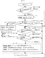
図10に傷がディスクにある場合の傷処理のシーケンスを示す。再生スタート(10A)させた後に、第一の傷検出部で、RF信号の傷を検出する(10B)。第一の傷検出部では、振幅が一定値以下の場合に傷と判断し、傷検出期間AGC回路をホールドする(10
C)。傷の影響が少なくなるようにするためである。傷が検出されない場合は、AGC回路が動作し、所定の振幅値を出力する。傷が無い場合は、次段のA/Dコンバータの標準入力にあわせた信号振幅を出力する。第一の傷検出部で傷が検出されない場合でも、A/D回路によりデジタル化された信号は、第二の欠陥検出部により傷があるかどうかどうかされる(10F)。
第一の傷検出部により、傷が検出された場合には、傷の位置を検出する(10D)。傷の場所が、ヘッダ部でアドレス以外である場合には、特に傷処理を行なわない。この部分は、PLLの再生クロックは、ウォブルに同期しているから、PLL回路の動作に影響を及ぼさないからである。また、再生しようとするアドレスデータがないためである。
FIG. 10 shows a sequence of scratch processing when scratches are present on the disk. After starting reproduction (10A), the first flaw detector detects a flaw in the RF signal (10B). The first flaw detection unit determines that a flaw is present when the amplitude is equal to or smaller than a certain value, and holds the flaw detection period AGC circuit (10
C). This is to reduce the influence of scratches. If no flaw is detected, the AGC circuit operates and outputs a predetermined amplitude value. If there is no damage, the signal amplitude is output in accordance with the standard input of the next stage A / D converter. Even if no scratch is detected by the first scratch detector, the signal digitized by the A / D circuit is checked by the second defect detector as to whether there is a scratch (10F).
When a scratch is detected by the first scratch detection unit, the position of the scratch is detected (10D). If the scratch location is other than the address in the header portion, no particular scratch processing is performed. This is because the PLL recovered clock is synchronized with the wobble and does not affect the operation of the PLL circuit. This is also because there is no address data to be reproduced.
ヘッダ部のアドレス情報ID1〜4の一部に傷があった場合について説明する。ID1〜4は、あらかじめ記録されたアドレスであり、ウォブルと同期がとれているため、PLLのロックは、もともと外れにくい。このため、PLL特性だけを考えると第二の傷検出(10F)の判断基準は、データ部の傷検出判断基準よりも余裕のある値に設定できる。次段の復調信号処理部12の再生処理能力等を考慮した値に設定しても良い。
The case where a part of address information ID1-4 of a header part has a damage | wound is demonstrated.
傷の場所がヘッダ(アドレス)/データ部の切り替わり部であった場合は、HPFの時定数は、小さいままにし、早く傷が整定できるようにする。傷期間は、オフセット補正部、位相比較器の出力はホールドまたは0に固定する。傷の後、一定期間、オフセット補正部の積分器の係数を、積分速度が早くなり、標本化再生信号のオフセットが早くなくなるような値に切り替える。 If the scratch location is the header (address) / data switching section, keep the HPF time constant small so that the scratch can be settled quickly. During the scratch period, the output of the offset correction unit and the phase comparator is held or fixed to zero. After the flaw, for a certain period, the coefficient of the integrator of the offset correction unit is switched to a value such that the integration speed is increased and the sampling reproduction signal is not offset earlier.
傷の場所が、データ部である場合は、第二の傷検出部にて標本化再生信号に傷がないかどうかの判断を行う(10F)。フィードバック処理で時間がかかるために、第一の傷検出部で取りこぼした傷やノイズのために、PLLのロックがはずれないようにするためである。 If the location of the flaw is the data portion, the second flaw detection portion determines whether the sampled reproduction signal is flawed (10F). This is because it takes time for the feedback processing, so that the PLL is not unlocked due to scratches and noises that are missed by the first scratch detection unit.
第二の傷検出部では、傷の種類により、PLL回路に対する処理を変える(10H)。指紋のように傷期間が短く、周期的に傷が検出されるときは、PLLのロックは外れにくく、再生信号も得やすいことから、特に傷に対応した処理は行わず、再生処理を行なう。 In the second flaw detection unit, processing for the PLL circuit is changed depending on the type of flaw (10H). When the scratch period is short, such as a fingerprint, and the scratch is periodically detected, the PLL is not easily unlocked and a reproduction signal can be easily obtained. Therefore, the reproduction process is performed without performing a process corresponding to the scratch.
ブラックドット等の傷期間が長い場合は、傷と判断し、オフセット補正部、位相比較器の出力はホールドまたは0に固定する。傷の後、一定期間、オフセット補正部の積分器の係数を、積分速度が早くなり、標本化再生信号のオフセットが早くなくなるような値に切り替える。(10I)
なお、以上の実施例ではDVD−RAMディスクを例に挙げ説明したが、本発明の適用範囲はDVD−RAM装置に限られるものではなく、DVD−RAMディスク以外の記録再生装置においても同様の制御方法を採用することができる。
If the scratch period of black dots or the like is long, it is determined as a scratch, and the outputs of the offset correction unit and the phase comparator are held or fixed to zero. After the flaw, for a certain period, the coefficient of the integrator of the offset correction unit is switched to a value such that the integration speed is increased and the sampling reproduction signal is not offset earlier. (10I)
In the above embodiment, the DVD-RAM disk has been described as an example. However, the scope of application of the present invention is not limited to the DVD-RAM device, and the same control is performed in a recording / reproducing apparatus other than the DVD-RAM disk. The method can be adopted.
1…光ディスク、2…スピンドルモータ、3…光ヘッド、4…I/V変換器、5…Wobble処理部、6…RFデータ処理部、61…AGC、62…HPF、63…EQ、620…Fc(カットオフ周波数)調整部、7…第一の傷検出部、8…傷処理方法選択部、9…制御部、10…ホストコンピュータ、11…PLL部、12…復調信号処理部、110…A/D変換器、111…はVCO、112…D/A変換器、113…位相比較器、114…オフセット補正部、1140…積分器速度調整部、116…第二の傷検出部。
DESCRIPTION OF
Claims (4)
前記光ディスクから再生した再生信号の振幅が一定値より低いことを欠陥として検出する第1の欠陥検出手段と、
位相同期帰還回路に備えられ、該再生信号を再生クロックに基づいて標本化し標本化再生信号を得るアナログデジタル変換手段と、
該標本化再生信号の振幅に基づいて欠陥を検出する第2の欠陥検出手段と、
前記標本化再生信号のオフセットを補正するオフセット補正手段と、
前記位相同期帰還回路に備えられ、前記標本化再生信号に基づいて位相誤差を示す信号を出力する位相比較手段と、
を具備しており、
該オフセット補正手段は、
前記標本化再生信号を積分する機能と、
前記標本化再生信号から積分値を減算することによりオフセットを補正する機能と、
積分速度を可変する機能と、を有し、
前記第1の欠陥検出手段が欠陥を検出している間に、前記再生信号のゲインをホールドし、前記第2の欠陥検出手段が欠陥を検出しなくなった後に、前記オフセット補正手段により前記積分速度を増加させ、
前記第2の欠陥検出手段により欠陥を検出した場合には、前記オフセット補正手段は、前記オフセットをホールドまたは0に固定し、
前記第2の欠陥検出手段と前記オフセット補正手段とは、前記アナログデジタル変換手段と、前記位相比較手段との間に配置され、前記位相比較手段には、前記オフセット補正手段によりオフセットを補正された標本化再生信号が入力される
ことを特徴とする光ディスク装置。 An optical disc apparatus for recording / reproducing information on / from an optical disc provided with a header area in which address information is recorded and a data area in which user information can be recorded,
First defect detection means for detecting as a defect that the amplitude of a reproduction signal reproduced from the optical disc is lower than a certain value;
An analog-to-digital conversion means provided in a phase-synchronized feedback circuit for obtaining the sampled reproduction signal by sampling the reproduction signal based on the reproduction clock;
Second defect detection means for detecting a defect based on the amplitude of the sampling reproduction signal;
Offset correction means for correcting an offset of the sampling reproduction signal;
Phase comparison means provided in the phase-synchronized feedback circuit for outputting a signal indicating a phase error based on the sampled reproduction signal;
It has
The offset correction means includes
A function of integrating the sampled reproduction signal;
A function of correcting an offset by subtracting an integral value from the sampling reproduction signal;
A function of varying the integration speed,
While the first defect detection means detects a defect, the gain of the reproduction signal is held, and after the second defect detection means no longer detects a defect, the offset correction means performs the integration speed. Increase
When a defect is detected by the second defect detection means, the offset correction means fixes the offset to hold or 0,
The second defect detection unit and the offset correction unit are disposed between the analog-digital conversion unit and the phase comparison unit, and the phase comparison unit has an offset corrected by the offset correction unit. An optical disc apparatus to which a sampling reproduction signal is inputted .
前記第1または第2の欠陥検出手段で判断された、欠陥種類、欠陥位置の情報から、欠陥処理方法を選択する処理方法選択手段を備えることを特徴とする光ディスク装置。 In claim 1,
An optical disc apparatus comprising processing method selection means for selecting a defect processing method from information on a defect type and a defect position determined by the first or second defect detection means.
前記光ディスク装置は、前記再生信号の高周波成分を濾波するHPFと、 The optical disc apparatus includes an HPF for filtering high frequency components of the reproduction signal,
前記ヘッダ領域のアドレスの前後に対して前記HPFのカットオフ周波数を変化させる処理手段と、を有し、 Processing means for changing the cutoff frequency of the HPF before and after the address of the header region,
前記第1の欠陥検出手段は、前記HPFにより濾波された再生信号に基づいて欠陥を検出し、 The first defect detection means detects a defect based on the reproduction signal filtered by the HPF,
前記第1の欠陥検出手段と前記処理方法選択手段の結果により、前記HPFのカットオフ周波数を可変する時間を制御すること特徴とする光ディスク装置。 An optical disc apparatus, wherein a time for varying the cut-off frequency of the HPF is controlled according to the results of the first defect detection means and the processing method selection means.
前記オフセット補正手段は、前記標本化再生信号の振幅を制限するリミッタを有し、 The offset correction means has a limiter for limiting the amplitude of the sampling reproduction signal,
傷を検出した後一定期間は、前記リミッタを用いずに高速にオフセット補正し、 For a certain period after detecting the scratch, the offset is corrected at high speed without using the limiter,
その他の場合は、前記リミッタを用いて、誤差を少なくするオフセット補正することを特徴とする光ディスク装置。In other cases, the optical disk apparatus is characterized in that offset correction is performed to reduce errors using the limiter.
Priority Applications (1)
| Application Number | Priority Date | Filing Date | Title |
|---|---|---|---|
| JP2003379292A JP4625623B2 (en) | 2003-11-10 | 2003-11-10 | Optical disk playback device |
Applications Claiming Priority (1)
| Application Number | Priority Date | Filing Date | Title |
|---|---|---|---|
| JP2003379292A JP4625623B2 (en) | 2003-11-10 | 2003-11-10 | Optical disk playback device |
Publications (2)
| Publication Number | Publication Date |
|---|---|
| JP2005141868A JP2005141868A (en) | 2005-06-02 |
| JP4625623B2 true JP4625623B2 (en) | 2011-02-02 |
Family
ID=34689387
Family Applications (1)
| Application Number | Title | Priority Date | Filing Date |
|---|---|---|---|
| JP2003379292A Expired - Fee Related JP4625623B2 (en) | 2003-11-10 | 2003-11-10 | Optical disk playback device |
Country Status (1)
| Country | Link |
|---|---|
| JP (1) | JP4625623B2 (en) |
Families Citing this family (5)
| Publication number | Priority date | Publication date | Assignee | Title |
|---|---|---|---|---|
| JP2006344294A (en) | 2005-06-09 | 2006-12-21 | Hitachi Ltd | Information reproducing device and reproducing signal processing circuit |
| JP4823880B2 (en) | 2006-12-05 | 2011-11-24 | 株式会社日立製作所 | Optical disk drive with envelope abnormality detection function |
| JP2008181617A (en) * | 2007-01-25 | 2008-08-07 | Nec Corp | Information reproducing unit |
| JP5242284B2 (en) * | 2007-08-30 | 2013-07-24 | パナソニック株式会社 | Optical disc apparatus and optical pickup |
| JP4941573B2 (en) * | 2010-04-05 | 2012-05-30 | 株式会社日立製作所 | Information reproduction apparatus and reproduction signal processing circuit |
-
2003
- 2003-11-10 JP JP2003379292A patent/JP4625623B2/en not_active Expired - Fee Related
Also Published As
| Publication number | Publication date |
|---|---|
| JP2005141868A (en) | 2005-06-02 |
Similar Documents
| Publication | Publication Date | Title |
|---|---|---|
| JP2008282506A (en) | Circuit and method for processing reproduction signal, and optical disk drive | |
| JP3996601B2 (en) | Signal processing apparatus and signal processing method | |
| US7224659B2 (en) | Disk reproducing device with suppressed reproduction signal error | |
| JPH1186442A (en) | Information reproducing device | |
| JP3956436B2 (en) | Data demodulation method and optical disk apparatus using the same | |
| JP4955768B2 (en) | Input signal binarization apparatus and method, disk drive, and recording medium | |
| JP2006252681A (en) | Optical disk drive and pll circuit | |
| WO2001099108A1 (en) | Optical disk unit | |
| JP4625623B2 (en) | Optical disk playback device | |
| JP2005166121A (en) | Disk drive and disk reproduction method | |
| US20090052294A1 (en) | Information recording medium, information reproducing apparatus and information reproducing method | |
| JP3795218B2 (en) | Information playback device | |
| EP1443502A1 (en) | Defect signal detecting apparatus for optical recording/reproducing apparatus and defect signal detecting method thereof | |
| KR100556004B1 (en) | Reproduction signal processor and optical disk apparatus | |
| JP2007299448A (en) | Wide capture circuit | |
| US6597295B1 (en) | Decoding apparatus and decoding method | |
| US7200089B2 (en) | Disk reproducing device reproducing information recorded on recording medium by multiple recording devices | |
| US8102744B2 (en) | Recording medium playback device and recording medium playback method | |
| JP5054672B2 (en) | Device for accessing a recording medium | |
| JP3927561B2 (en) | Reproduction signal processing apparatus and optical disk apparatus | |
| CN116917990A (en) | Information recording/reproducing apparatus and information recording/reproducing method | |
| JP4446865B2 (en) | Information recording medium, synchronization signal generating method, information reproducing method, information reproducing device, information recording method, information recording device | |
| US7835244B2 (en) | Optical disc apparatus and ADIP decoder | |
| JPH11238297A (en) | Optical record medium discriminating method and its device | |
| JP3926779B2 (en) | Digital phase locked loop circuit |
Legal Events
| Date | Code | Title | Description |
|---|---|---|---|
| A621 | Written request for application examination |
Free format text: JAPANESE INTERMEDIATE CODE: A621 Effective date: 20060403 |
|
| RD04 | Notification of resignation of power of attorney |
Free format text: JAPANESE INTERMEDIATE CODE: A7424 Effective date: 20060515 |
|
| A977 | Report on retrieval |
Free format text: JAPANESE INTERMEDIATE CODE: A971007 Effective date: 20071029 |
|
| A131 | Notification of reasons for refusal |
Free format text: JAPANESE INTERMEDIATE CODE: A131 Effective date: 20071106 |
|
| A521 | Written amendment |
Free format text: JAPANESE INTERMEDIATE CODE: A523 Effective date: 20071227 |
|
| A02 | Decision of refusal |
Free format text: JAPANESE INTERMEDIATE CODE: A02 Effective date: 20080205 |
|
| A521 | Written amendment |
Free format text: JAPANESE INTERMEDIATE CODE: A523 Effective date: 20080331 |
|
| A911 | Transfer of reconsideration by examiner before appeal (zenchi) |
Free format text: JAPANESE INTERMEDIATE CODE: A911 Effective date: 20080415 |
|
| A912 | Removal of reconsideration by examiner before appeal (zenchi) |
Free format text: JAPANESE INTERMEDIATE CODE: A912 Effective date: 20080509 |
|
| A01 | Written decision to grant a patent or to grant a registration (utility model) |
Free format text: JAPANESE INTERMEDIATE CODE: A01 |
|
| A61 | First payment of annual fees (during grant procedure) |
Free format text: JAPANESE INTERMEDIATE CODE: A61 Effective date: 20101108 |
|
| R150 | Certificate of patent or registration of utility model |
Free format text: JAPANESE INTERMEDIATE CODE: R150 |
|
| FPAY | Renewal fee payment (event date is renewal date of database) |
Free format text: PAYMENT UNTIL: 20131112 Year of fee payment: 3 |
|
| LAPS | Cancellation because of no payment of annual fees |