JP4601552B2 - Resin composition for composite dielectric, composite dielectric, and electric circuit board using the dielectric - Google Patents
Resin composition for composite dielectric, composite dielectric, and electric circuit board using the dielectric Download PDFInfo
- Publication number
- JP4601552B2 JP4601552B2 JP2005514395A JP2005514395A JP4601552B2 JP 4601552 B2 JP4601552 B2 JP 4601552B2 JP 2005514395 A JP2005514395 A JP 2005514395A JP 2005514395 A JP2005514395 A JP 2005514395A JP 4601552 B2 JP4601552 B2 JP 4601552B2
- Authority
- JP
- Japan
- Prior art keywords
- dielectric
- composite dielectric
- composite
- liquid composition
- aromatic polymer
- Prior art date
- Legal status (The legal status is an assumption and is not a legal conclusion. Google has not performed a legal analysis and makes no representation as to the accuracy of the status listed.)
- Expired - Fee Related
Links
Images


Classifications
-
- H—ELECTRICITY
- H01—ELECTRIC ELEMENTS
- H01G—CAPACITORS; CAPACITORS, RECTIFIERS, DETECTORS, SWITCHING DEVICES, LIGHT-SENSITIVE OR TEMPERATURE-SENSITIVE DEVICES OF THE ELECTROLYTIC TYPE
- H01G4/00—Fixed capacitors; Processes of their manufacture
- H01G4/002—Details
- H01G4/018—Dielectrics
- H01G4/20—Dielectrics using combinations of dielectrics from more than one of groups H01G4/02 - H01G4/06
- H01G4/206—Dielectrics using combinations of dielectrics from more than one of groups H01G4/02 - H01G4/06 inorganic and synthetic material
-
- H—ELECTRICITY
- H10—SEMICONDUCTOR DEVICES; ELECTRIC SOLID-STATE DEVICES NOT OTHERWISE PROVIDED FOR
- H10K—ORGANIC ELECTRIC SOLID-STATE DEVICES
- H10K10/00—Organic devices specially adapted for rectifying, amplifying, oscillating or switching; Organic capacitors or resistors having potential barriers
- H10K10/40—Organic transistors
- H10K10/46—Field-effect transistors, e.g. organic thin-film transistors [OTFT]
- H10K10/462—Insulated gate field-effect transistors [IGFETs]
- H10K10/468—Insulated gate field-effect transistors [IGFETs] characterised by the gate dielectrics
- H10K10/478—Insulated gate field-effect transistors [IGFETs] characterised by the gate dielectrics the gate dielectric comprising a layer of composite material comprising interpenetrating or embedded materials, e.g. TiO2 particles in a polymer matrix
-
- C—CHEMISTRY; METALLURGY
- C08—ORGANIC MACROMOLECULAR COMPOUNDS; THEIR PREPARATION OR CHEMICAL WORKING-UP; COMPOSITIONS BASED THEREON
- C08L—COMPOSITIONS OF MACROMOLECULAR COMPOUNDS
- C08L101/00—Compositions of unspecified macromolecular compounds
- C08L101/02—Compositions of unspecified macromolecular compounds characterised by the presence of specified groups, e.g. terminal or pendant functional groups
- C08L101/04—Compositions of unspecified macromolecular compounds characterised by the presence of specified groups, e.g. terminal or pendant functional groups containing halogen atoms
-
- C—CHEMISTRY; METALLURGY
- C08—ORGANIC MACROMOLECULAR COMPOUNDS; THEIR PREPARATION OR CHEMICAL WORKING-UP; COMPOSITIONS BASED THEREON
- C08K—Use of inorganic or non-macromolecular organic substances as compounding ingredients
- C08K3/00—Use of inorganic substances as compounding ingredients
-
- H—ELECTRICITY
- H05—ELECTRIC TECHNIQUES NOT OTHERWISE PROVIDED FOR
- H05K—PRINTED CIRCUITS; CASINGS OR CONSTRUCTIONAL DETAILS OF ELECTRIC APPARATUS; MANUFACTURE OF ASSEMBLAGES OF ELECTRICAL COMPONENTS
- H05K1/00—Printed circuits
- H05K1/16—Printed circuits incorporating printed electric components, e.g. printed resistors, capacitors or inductors
- H05K1/162—Printed circuits incorporating printed electric components, e.g. printed resistors, capacitors or inductors incorporating printed capacitors
-
- H—ELECTRICITY
- H05—ELECTRIC TECHNIQUES NOT OTHERWISE PROVIDED FOR
- H05K—PRINTED CIRCUITS; CASINGS OR CONSTRUCTIONAL DETAILS OF ELECTRIC APPARATUS; MANUFACTURE OF ASSEMBLAGES OF ELECTRICAL COMPONENTS
- H05K2201/00—Indexing scheme relating to printed circuits covered by H05K1/00
- H05K2201/01—Dielectrics
- H05K2201/0137—Materials
- H05K2201/015—Fluoropolymer, e.g. polytetrafluoroethylene [PTFE]
-
- H—ELECTRICITY
- H05—ELECTRIC TECHNIQUES NOT OTHERWISE PROVIDED FOR
- H05K—PRINTED CIRCUITS; CASINGS OR CONSTRUCTIONAL DETAILS OF ELECTRIC APPARATUS; MANUFACTURE OF ASSEMBLAGES OF ELECTRICAL COMPONENTS
- H05K2201/00—Indexing scheme relating to printed circuits covered by H05K1/00
- H05K2201/02—Fillers; Particles; Fibers; Reinforcement materials
- H05K2201/0203—Fillers and particles
- H05K2201/0206—Materials
- H05K2201/0209—Inorganic, non-metallic particles
-
- H—ELECTRICITY
- H05—ELECTRIC TECHNIQUES NOT OTHERWISE PROVIDED FOR
- H05K—PRINTED CIRCUITS; CASINGS OR CONSTRUCTIONAL DETAILS OF ELECTRIC APPARATUS; MANUFACTURE OF ASSEMBLAGES OF ELECTRICAL COMPONENTS
- H05K2203/00—Indexing scheme relating to apparatus or processes for manufacturing printed circuits covered by H05K3/00
- H05K2203/07—Treatments involving liquids, e.g. plating, rinsing
- H05K2203/0756—Uses of liquids, e.g. rinsing, coating, dissolving
- H05K2203/0759—Forming a polymer layer by liquid coating, e.g. a non-metallic protective coating or an organic bonding layer
Landscapes
- Engineering & Computer Science (AREA)
- Chemical & Material Sciences (AREA)
- Microelectronics & Electronic Packaging (AREA)
- Power Engineering (AREA)
- Chemical Kinetics & Catalysis (AREA)
- Medicinal Chemistry (AREA)
- Polymers & Plastics (AREA)
- Organic Chemistry (AREA)
- Composite Materials (AREA)
- Materials Engineering (AREA)
- Inorganic Chemistry (AREA)
- Manufacturing & Machinery (AREA)
- Health & Medical Sciences (AREA)
- Compositions Of Macromolecular Compounds (AREA)
- Laminated Bodies (AREA)
- Inorganic Insulating Materials (AREA)
Description
本発明は、有機ポリマーと無機誘電体とからなる有機−無機複合誘電体用液状組成物と、該組成物を用いてなる複合誘電体、さらに、該誘電体を使用した電気回路基板に関する。The present invention relates to a liquid composition for an organic-inorganic composite dielectric composed of an organic polymer and an inorganic dielectric, a composite dielectric using the composition, and an electric circuit board using the dielectric.
情報化社会の進行とともに、情報伝達の高速度化、これに伴う情報信号の高周波化のニーズがますます高まりつつある。これに対応するため、エレクトロニクス製品に使用される回路基板の高機能化・高密度実装が求められ、この課題を解決するため、抵抗・キャパシター・インダクターといった電子素子を回路基板の中に作りこむ技術であるEPD(Embedded Passive Device Techinology)が注目を集めている。With the progress of the information society, there is an increasing need for high-speed information transmission and high-frequency information signals. To meet this demand, circuit boards used in electronics products are required to have high functionality and high-density mounting. To solve this problem, technology to create electronic elements such as resistors, capacitors, and inductors in the circuit board. EPD (Embedded Passive Device Technology) is attracting attention.
一般に実装に使用されるキャパシターにはセラミック誘電体が用いられているが、EPDに使用した場合に回路基板の孔あけや切断等の後加工性や、接着性が悪いことが問題となる。そこで、後加工性や接着性に優れた誘電体として有機ポリマーと無機誘電体を複合化した有機−無機複合誘電体が提案されている。In general, a ceramic dielectric is used for a capacitor used for mounting. However, when used for EPD, there is a problem that post-workability such as drilling and cutting of a circuit board and adhesion are poor. Therefore, an organic-inorganic composite dielectric material in which an organic polymer and an inorganic dielectric material are combined has been proposed as a dielectric material excellent in post-workability and adhesiveness.
この有機−無機複合誘電体は、ポリフェニレンオキシド樹脂やエポキシ樹脂等に誘電率の大きい無機誘電体を分散させて成形あるいは成膜させたものである(特許文献1参照)が、これらの樹脂は特に高周波域での誘電率が低いため、誘電率の大きい無機誘電体をできるだけ多く配合することが必要である。しかし、従来使用されているポリフェニレンオキシド樹脂やエポキシ樹脂では、無機誘電体の分散性に劣るため配合量に限界があり、複合誘電体としての誘電率は満足いくレベルには達していない。
そこで本発明では、有機ポリマーへの無機誘電体の分散性に優れ、有機−無機複合誘電体とした場合に、高い誘電率をしめす有機−無機複合誘電体用液状組成物を提供することを課題としている。Accordingly, the present invention has an object to provide a liquid composition for an organic-inorganic composite dielectric that exhibits excellent dispersibility of an inorganic dielectric in an organic polymer and exhibits a high dielectric constant when an organic-inorganic composite dielectric is used. It is said.
前記課題を解決するため、この発明にかかる複合誘電体用液状組成物では、無機誘電体とフッ素化芳香族ポリマーを含有することが特徴である。有機ポリマーとしてフッ素化芳香族ポリマーを使用すると、フッ素化芳香族ポリマーは無機誘電体の分散性に優れるため、組成物中に無機誘電体を高配合することができ、複合誘電体として高い誘電率をしめすものが得られる。このため、本発明の複合誘電体用液状組成物により形成される複合誘電体は、複合誘電体が用いられる用途の中でも、電気回路基板を構成するコンデンサー等の電子素子としての使用に好適なものとなる。In order to solve the above problems, the liquid composition for composite dielectric according to the present invention is characterized by containing an inorganic dielectric and a fluorinated aromatic polymer. When a fluorinated aromatic polymer is used as the organic polymer, the fluorinated aromatic polymer is excellent in dispersibility of the inorganic dielectric, so that the inorganic dielectric can be highly blended in the composition, and a high dielectric constant as a composite dielectric Can be obtained. For this reason, the composite dielectric formed by the liquid composition for composite dielectric of the present invention is suitable for use as an electronic element such as a capacitor constituting an electric circuit board, among uses where the composite dielectric is used. It becomes.
また、上記組成物は、無機誘電体が、フッ素化芳香族ポリマー100質量部に対して、700〜2000質量部の範囲にあり、該フッ素化芳香族ポリマーは、20℃〜80℃の反応温度で合成されたものであって、後述する一般式(1)で表される繰り返し単位を含むものであり、該一般式(1)で表される繰り返し単位のうち少なくとも1つが9,9−ビス(4−ヒドロキシフェニル)フルオレン骨格を含むことを特徴とする。これにより、高い誘電率の複合誘電体を得るために高い割合で無機誘電体を配合しても、良好な成膜性を維持することができる。 In the composition, the inorganic dielectric is in the range of 700 to 2000 parts by mass with respect to 100 parts by mass of the fluorinated aromatic polymer, and the fluorinated aromatic polymer has a reaction temperature of 20 to 80 ° C. In which at least one of the repeating units represented by the general formula (1) is 9,9-bis. (4-Hydroxyphenyl) fluorene skeleton is included. Thereby, even if an inorganic dielectric is blended at a high ratio in order to obtain a composite dielectric having a high dielectric constant, good film formability can be maintained.
さらに、本発明には、上記の複合誘電体用液状組成物を用いてなる複合誘電体や、該複合誘電体を構成部位として含む電気回路基板も含まれる。Furthermore, the present invention also includes a composite dielectric using the above-described composite dielectric liquid composition, and an electric circuit board including the composite dielectric as a constituent part.
なお、本発明の複合誘電体とは、無機誘電体を分散させた液状組成物を所定の形状に成形したものをいい、有機ポリマー中に無機誘電体が高分散された成形体および成形膜等を表す。The composite dielectric of the present invention refers to a liquid composition in which an inorganic dielectric is dispersed into a predetermined shape, such as a molded body and a molded film in which an inorganic dielectric is highly dispersed in an organic polymer. Represents.
本発明者等は、有機ポリマーに無機誘電体を分散させる有機−無機複合誘電体用液状組成物について鋭意検討を重ねた結果、有機ポリマーとしてフッ素化芳香族ポリマーを含むことにより、組成物中の無機誘電体の配合量を高めることができ、複合誘電体の特に高周波域での誘電率が格段に向上することを見出し、上記の課題をみごと解決できることに想到した。As a result of intensive studies on a liquid composition for an organic-inorganic composite dielectric material in which an inorganic dielectric is dispersed in an organic polymer, the present inventors have included a fluorinated aromatic polymer as the organic polymer. The amount of the inorganic dielectric can be increased, and the dielectric constant of the composite dielectric, particularly in the high frequency region, has been found to be significantly improved.
本発明の複合誘電体用液状組成物は、フッ素化芳香族ポリマーと無機誘電体を含有する。
本発明の複合誘電体用液状組成物において、フッ素化芳香族ポリマーと無機誘電体の含有量は、フッ素化芳香族ポリマーの100質量部に対して、無機誘電体が100〜2,000質量部の範囲内であることが好ましい。無機誘電体の含有量が100質量部未満では、液状組成物からなる複合誘電体の誘電率が低くなる恐れがある。一方、無機誘電体の含有量が2,000質量部を超えると該組成物の粘度が高くなり、取り扱い性が低下する恐れがある。無機誘電体の含有量のより好ましい下限は、フッ素化芳香族ポリマーの100質量部に対して500質量部以上であり、700質量部以上が最も好ましい。また、無機誘電体の含有量の好ましい上限は、フッ素化芳香族ポリマーの100質量部に対して1,500質量部以下であり、1,000質量部以下であることがさらに好ましい。
本発明の複合誘電体用液状組成物は、フッ素化芳香族ポリマー及び無機誘電体をそれぞれ1種又は2種以上含有することができる。The liquid composition for composite dielectric of the present invention contains a fluorinated aromatic polymer and an inorganic dielectric.
In the composite dielectric liquid composition of the present invention, the content of the fluorinated aromatic polymer and the inorganic dielectric is 100 to 2,000 parts by mass of the inorganic dielectric with respect to 100 parts by mass of the fluorinated aromatic polymer. It is preferable to be within the range. If the content of the inorganic dielectric is less than 100 parts by mass, the dielectric constant of the composite dielectric made of the liquid composition may be lowered. On the other hand, when the content of the inorganic dielectric exceeds 2,000 parts by mass, the viscosity of the composition increases, and the handleability may be reduced. The minimum with more preferable content of an inorganic dielectric material is 500 mass parts or more with respect to 100 mass parts of a fluorinated aromatic polymer, and 700 mass parts or more is the most preferable. Moreover, the upper limit with preferable content of an inorganic dielectric material is 1500 mass parts or less with respect to 100 mass parts of a fluorinated aromatic polymer, and it is still more preferable that it is 1,000 mass parts or less.
The liquid composition for a composite dielectric according to the present invention may contain one or more fluorinated aromatic polymers and inorganic dielectrics.
本発明におけるフッ素化芳香族ポリマーとしては、ガラス転移点温度が150℃以上であることが好ましい。ガラス転移点温度が150℃未満では、液状組成物からなる複合誘電体の耐熱性が低下するおそれがある。フッ素化芳香族ポリマーのガラス転移点温度は150℃〜400℃の範囲内がさらに好ましく、170℃〜300℃の範囲内が最も好ましい。ガラス転移温度は、例えば、DSC(セイコー電子工業社製、商品名「DSC6200」)を用いて、窒素雰囲気下、20℃/分の昇温速度の条件で測定することができる。The fluorinated aromatic polymer in the present invention preferably has a glass transition temperature of 150 ° C. or higher. When the glass transition temperature is less than 150 ° C., the heat resistance of the composite dielectric made of the liquid composition may be lowered. The glass transition temperature of the fluorinated aromatic polymer is more preferably in the range of 150 ° C to 400 ° C, and most preferably in the range of 170 ° C to 300 ° C. The glass transition temperature can be measured, for example, using DSC (trade name “DSC6200” manufactured by Seiko Denshi Kogyo Co., Ltd.) under a nitrogen atmosphere and a temperature increase rate of 20 ° C./min.
本発明のフッ素化芳香族ポリマーの表面抵抗値は、1.0×10¹⁵Ω/cm2以上であることが好ましい。表面抵抗値が1.0×1015Ω/cm2以上未満では、液状組成物からなる複合誘電体の絶縁性が低下する恐れがある。フッ素化芳香族ポリマーの表面抵抗値は1.0×1017Ω/cm2以上の範囲内がさらに好ましい。表面抵抗値は、例えば、抵抗値測定装置(ヒューレットパッカード(HEWLETT PACKERD)製、商品名「High Resistance Meter 4329A & Resistivity Cell 16008A」)を用いて、測定電圧500Vの条件で測定することができる。The surface resistance value of the fluorinated aromatic polymer of the present invention is preferably 1.0 × 10 15 Ω / cm 2 or more. If the surface resistance value is less than 1.0 × 10 15 Ω / cm 2 or more, the insulating property of the composite dielectric made of the liquid composition may be lowered. The surface resistance value of the fluorinated aromatic polymer is more preferably in the range of 1.0 × 10 17 Ω / cm 2 or more. The surface resistance value can be measured under the condition of a measurement voltage of 500 V using, for example, a resistance value measurement device (manufactured by Hewlett Packard, trade name “High Resistance Meter 4329A & Resistivity Cell 16008A”).
本発明のフッ素化芳香族ポリマーの平均分子量は、数平均分子量(Mn)で5,000〜500,000の範囲内であることが好ましい。数平均分子量が5,000未満では液状組成物からなる複合誘電体の耐熱性が低下するおそれがあり、数平均分子量が500,000を超えると樹脂組成物の粘度が高くなり、作業性が低下する。The average molecular weight of the fluorinated aromatic polymer of the present invention is preferably in the range of 5,000 to 500,000 in terms of number average molecular weight (Mn). If the number average molecular weight is less than 5,000, the heat resistance of the composite dielectric made of a liquid composition may be reduced. If the number average molecular weight exceeds 500,000, the viscosity of the resin composition increases and the workability decreases. To do.
上記数平均分子量(Mn)は10,000〜200,000の範囲内がさらに好ましく、10,000〜100,000の範囲内が最も好ましい。数平均分子量は、例えば、ゲルパーミエーションクロマトグラフ分析装置(GPC)(東ソー社製、商品名「HLC−8120GPC」)を用いて、カラムとしてG−5000HXL+GMHXL−L、展開溶媒としてTHF、標準として標準ポリスチレンを用い、流量1mL/分の条件で測定することができる。The number average molecular weight (Mn) is more preferably in the range of 10,000 to 200,000, and most preferably in the range of 10,000 to 100,000. The number average molecular weight is, for example, G-5000HXL + GMHXL-L as a column, THF as a developing solvent, standard as a standard using a gel permeation chromatograph analyzer (GPC) (trade name “HLC-8120GPC” manufactured by Tosoh Corporation). Using polystyrene, the measurement can be performed under a flow rate of 1 mL / min.
本発明のフッ素化芳香族ポリマーは、少なくとも1つ以上のフッ素基を有する芳香族環と、エーテル結合、ケトン結合、スルホン結合、アミド結合、イミド結合、エステル結合の群より選ばれた少なくとも1つの結合を含む繰り返し単位により構成された重合体であり、具体的には、例えば、フッ素原子を有するポリイミド、ポリエーテル、ポリエーテルイミド、ポリエーテルケトン、ポリエーテルスルホン、ポリアミドエーテル、ポリアミド、ポリエーテルニトリル、ポリエステルなどが挙げられる。The fluorinated aromatic polymer of the present invention has at least one selected from the group consisting of an aromatic ring having at least one fluorine group and an ether bond, a ketone bond, a sulfone bond, an amide bond, an imide bond, and an ester bond. A polymer composed of a repeating unit containing a bond, specifically, for example, fluorine-containing polyimide, polyether, polyetherimide, polyether ketone, polyether sulfone, polyamide ether, polyamide, polyether nitrile And polyester.
本発明のフッ素化芳香族ポリマーは、少なくとも1つ以上のフッ素基を有する芳香族環と、エーテル結合を含む繰り返し単位を必須部位として有する重合体であることが好ましい。
さらに、本発明のフッ素化芳香族ポリマーは、下記一般式(1)で表される繰り返し単位を含むフッ素原子を有するポリアリールエーテルであることが好ましい。フッ素含有芳香族ポリマーがこのような構造を有するものであると、無機誘電体との相互作用が適度に抑制されると考えられ、複合誘電体用液状組成物作製に支障をきたす現象、例えば大幅な増粘、ゲル化、流動性の損失、凝集等が低減される。よって、より多くの無機誘電体を配合した複合誘電体用液状組成物を作製することができ、複合誘電体としてより高い誘電率を示すものとすることができるだけでなく、粘度を低下させることができるため、複合誘電体を薄膜状に成形することが容易となる。なお、一般式(1)で表される繰り返し単位は、同一でも異なっていてもよく、ブロック状、ランダム状等の何れの形態であってもよい。The fluorinated aromatic polymer of the present invention is preferably a polymer having, as essential sites, an aromatic ring having at least one fluorine group and a repeating unit containing an ether bond.
Furthermore, the fluorinated aromatic polymer of the present invention is preferably a polyaryl ether having a fluorine atom containing a repeating unit represented by the following general formula (1). If the fluorine-containing aromatic polymer has such a structure, it is considered that the interaction with the inorganic dielectric is moderately suppressed, and a phenomenon that hinders the preparation of a liquid composition for a composite dielectric, for example, Thickening, gelation, loss of fluidity, aggregation, etc. are reduced. Therefore, it is possible to produce a liquid composition for a composite dielectric containing a larger amount of inorganic dielectric, and not only can have a higher dielectric constant as a composite dielectric, but also can reduce the viscosity. Therefore, the composite dielectric can be easily formed into a thin film. The repeating units represented by the general formula (1) may be the same or different, and may be in any form such as a block form or a random form.
(式中、Rは同一又は異なる炭素数1〜150の芳香族環を有する2価の有機鎖を表す。また、Zは2価の鎖又は直接結合を表す。m及びm’は0以上の整数であり、m+m’=1〜8を満たし、同一又は異なって芳香族環に結合しているフッ素原子の数を表す。nは、重合度を表わし、2〜5000の範囲内が好ましく、5〜500の範囲内がさらに好ましい。)(In the formula, R represents a divalent organic chain having the same or different aromatic ring having 1 to 150 carbon atoms. Z represents a divalent chain or a direct bond. M and m ′ are 0 or more. It is an integer and represents the number of fluorine atoms that satisfy m + m ′ = 1 to 8, and are the same or different and bonded to the aromatic ring, n represents the degree of polymerization, preferably in the range of 2 to 5000. More preferably within the range of ~ 500.)
上記一般式(1)において、m+m’は2〜8の範囲内が好ましく、4〜8の範囲内がさらに好ましい。In the general formula (1), m + m ′ is preferably in the range of 2 to 8, more preferably in the range of 4 to 8.
上記一般式(1)において、エーテル構造部分(−O−R−O−)が芳香環に結合している位置については、Zに対してパラ位に結合していることが好ましい。In the general formula (1), the position where the ether structure moiety (—O—R—O—) is bonded to the aromatic ring is preferably bonded to the para position relative to Z.
上記一般式(1)において、Rは2価の有機鎖であるが、下記の構造式群(2)で表されるいずれか一つ、あるいは、その組み合わせの有機鎖であることが好ましい。In the general formula (1), R is a divalent organic chain, and is preferably any one of the following structural formula groups (2) or a combination thereof.
(式中、Y1〜Y4は、同一又は異なって水素基または置換基を表し、該置換基は、アルキル基、アルコキシル基を表す。)(In formula, Y < 1 > -Y < 4 > is the same or different and represents a hydrogen group or a substituent, and this substituent represents an alkyl group and an alkoxyl group.)
上記Rのより好ましい、具体例としては、下記の構造式群(3)で表される有機鎖が挙げられる。Specific examples of more preferable R include organic chains represented by the following structural formula group (3).
上記一般式(1)において、Zは、2価の鎖又は直接結合していることを表す。該2価の鎖としては、例えば、下記構造式群(4)で表される鎖であることが好ましい。In the general formula (1), Z represents a divalent chain or a direct bond. The divalent chain is preferably, for example, a chain represented by the following structural formula group (4).
(式中、Xは、炭素数1〜50の2価の有機鎖である。)(In the formula, X is a divalent organic chain having 1 to 50 carbon atoms.)
上記Xは、例えば、構造式群(3)で表される有機鎖が挙げられ、その中でもジフェニルエーテル鎖、ビスフェノールA鎖、ビスフェノールF鎖、フルオレン鎖が好ましい。Examples of X include an organic chain represented by the structural formula group (3), and among them, a diphenyl ether chain, a bisphenol A chain, a bisphenol F chain, and a fluorene chain are preferable.
本発明のフッ素化芳香族ポリマーの合成方法としては、一般的な重合反応を用いればよく、例えば、縮合重合、付加重合、溶液重合、懸濁重合、乳化重合等が挙げられる。上記重合反応の際の反応温度や反応時間等の反応条件は適宜設定すればよい。また、上記重合反応は、窒素雰囲気下で行うことが好ましい。As a method for synthesizing the fluorinated aromatic polymer of the present invention, a general polymerization reaction may be used, and examples thereof include condensation polymerization, addition polymerization, solution polymerization, suspension polymerization, and emulsion polymerization. What is necessary is just to set reaction conditions, such as reaction temperature and reaction time in the case of the said polymerization reaction, suitably. Moreover, it is preferable to perform the said polymerization reaction in nitrogen atmosphere.
例えば、上記一般式(1)で表される繰り返し単位を含むフッ素原子を有するポリアリールエーテルの合成方法を挙げると、Zが上記構造式群(4)のうちの(4−6)であり、さらに、Xがジフェニルエーテル鎖であるフッ素原子を有するポリアリールエーテルを得る場合、有機溶媒中、塩基性化合物の存在下で、4,4′−ビス(2,3,4,5,6−ペンタフルオロベンゾイル)ジフェニルエーテル(以下、「BPDE」という)と2価のフェノール化合物を加熱する方法等が挙げられる。For example, when synthesizing a polyaryl ether having a fluorine atom containing a repeating unit represented by the general formula (1), Z is (4-6) in the structural formula group (4). Furthermore, when obtaining a polyaryl ether having a fluorine atom in which X is a diphenyl ether chain, 4,4′-bis (2,3,4,5,6-pentafluoro in an organic solvent in the presence of a basic compound. And a method of heating benzoyl) diphenyl ether (hereinafter referred to as “BPDE”) and a divalent phenol compound.
上記の合成方法における反応温度としては、20℃〜150℃の範囲内が好ましく、50℃〜120℃の範囲内がさらに好ましい。As reaction temperature in said synthesis method, the inside of the range of 20 to 150 degreeC is preferable, and the inside of the range of 50 to 120 degreeC is further more preferable.
上記の合成方法で使用される有機溶媒としては、例えば、N−メチル−2−ピロリドン(NMP)、N,N−ジメチルアセトアミドやメタノール等の極性溶媒やトルエン等の芳香族系溶媒が挙げられる。Examples of the organic solvent used in the synthesis method include polar solvents such as N-methyl-2-pyrrolidone (NMP), N, N-dimethylacetamide and methanol, and aromatic solvents such as toluene.
上記の合成方法で使用される塩基性化合物としては、例えば、炭酸カリウム、炭酸リチウム、水酸化カリウム等が挙げられる。Examples of the basic compound used in the above synthesis method include potassium carbonate, lithium carbonate, potassium hydroxide and the like.
上記の合成方法において、2価のフェノール化合物としては、例えば、2,2−ビス(4−ヒドロキシフェニル)−1,1,1,3,3,3−ヘキサフルオロプロパン(以下、「6FBA」という)、ビスフェノールA(以下、「BA」という)、9,9−ビス(4−ヒドロキシフェニル)フルオレン(以下、「HF」という)、ビスフェノールF、ハイドロキノン、レゾルシノール等が挙げられる。In the above synthesis method, examples of the divalent phenol compound include 2,2-bis (4-hydroxyphenyl) -1,1,1,3,3,3-hexafluoropropane (hereinafter referred to as “6FBA”). ), Bisphenol A (hereinafter referred to as “BA”), 9,9-bis (4-hydroxyphenyl) fluorene (hereinafter referred to as “HF”), bisphenol F, hydroquinone, resorcinol and the like.
上記2価のフェノール化合物の使用量は、4,4′−ビス(2,3,4,5,6−ペンタフルオロベンゾイル)ジフェニルエーテル1モルに対して、0.8〜1.2モルの範囲内が好ましく、0.9〜1.1モルの範囲内がさらに好ましい。The amount of the divalent phenol compound used is in the range of 0.8 to 1.2 mol per mol of 4,4′-bis (2,3,4,5,6-pentafluorobenzoyl) diphenyl ether. Is preferable, and the range of 0.9 to 1.1 mol is more preferable.
上記の合成方法においては、反応終了後に、反応溶液より溶媒除去を行ない、必要により留去物を洗浄することにより、フッ素化芳香族ポリマーが得られる。また、反応溶液にフッ素化芳香族ポリマーの溶解度の低い溶媒中に加えることにより、該ポリマーを沈殿させ、沈殿物を濾過により分離することにより得ることもできる。In the above synthesis method, after completion of the reaction, the solvent is removed from the reaction solution, and the distillate is washed as necessary to obtain a fluorinated aromatic polymer. It can also be obtained by adding the fluorinated aromatic polymer to the reaction solution in a solvent with low solubility to precipitate the polymer and separating the precipitate by filtration.
本発明における無機誘電体としては、ペルブスカイト結晶構造を有するABO3型の誘電体およびこの2元系または3元系の複合ペルブスカイト系誘電体が好ましく、その他、酸化チタンも用いることができる。As the inorganic dielectric in the present invention, an ABO 3 type dielectric having a perovskite crystal structure and a binary or ternary composite perovskite dielectric are preferable, and titanium oxide can also be used.
上記ABO3型の誘電体としては、例えば、チタン酸鉛PbTiO3、タングステン酸鉛PbWO3、亜鉛酸鉛PbZnO3、鉄酸鉛PbFeO3、マグネシウム酸鉛PbMgO3、ニオブ酸鉛PbZbO3、ニッケル酸鉛PbNiO3、ジルコン酸鉛PbZrO3、チタン酸バリウムBaTiO3、チタン酸ストロンチウムSrTiO3、ジルコン酸カルシウムCaZrO3、チタン酸カルシウムCaTiO3、チタン酸亜鉛ZnTiO3、チタン酸マグネシウムZnTiO3、ジルコン酸バリウムBaZrO3、ジルコン酸マグネシウムMgZrO3、ジルコン酸亜鉛ZnZrO3等が挙げられる。The dielectric of the ABO 3 type, for example, lead titanate PbTiO 3, lead tungstate PbWO 3, zinc, lead PbZnO 3, Tetsusan'namari PbFeO 3, magnesium lead PbMgO 3, lead niobate PbZbO 3, nickelate Lead PbNiO 3 , lead zirconate PbZrO 3 , barium titanate BaTiO 3 , strontium titanate SrTiO 3 , calcium zirconate CaZrO 3 , calcium titanate CaTiO 3 , zinc titanate ZnTiO 3 , magnesium titanate ZnTiO 3 a , barium zirconate B a 3 , magnesium zirconate MgZrO 3 , zinc zirconate ZnZrO 3 and the like.
上記2元系または3元系の複合ペルブスカイト系誘電体としては、例えば、(BaxSr(1− x))(SnyTi(1−y))O3、Ba(TixSn(1−x))O3、BaxSr(1−x)TiO3、BaTiO3−CaZrO3、BaTiO3−Bi4Ti3O12、(BaxCa(1−x))(ZryTiO(1−y))O3等が挙げられる。As the composite Perubusukaito based dielectric of the binary or ternary, for example, (Ba x Sr (1- x )) (Sn y Ti (1-y))
本発明の無機誘電体の形状としては、粒子状、繊維状、燐片状、円錐状等が挙げられる。Examples of the shape of the inorganic dielectric of the present invention include particles, fibers, flakes, and cones.
上記無機誘電体の平均粒子径としては、液状組成物を用いてなる複合誘電体の厚みを考慮して適宜選択されるが、薄膜として用いる場合には、0.01〜10μmの範囲内であることが好ましく、0.1〜5μmの範囲内であることがさらに好ましく、0.5〜3μmの範囲内が最も好ましい。また、無機誘電体の体積当たりの比表面積は、1m2/g〜10m2/gの範囲内が好ましく、2m2/g〜8m2/gの範囲内がさらに好ましく、2m2/cg〜5m2/gの範囲内が最も好ましい。The average particle size of the inorganic dielectric is appropriately selected in consideration of the thickness of the composite dielectric using the liquid composition, but when used as a thin film, it is within the range of 0.01 to 10 μm. It is more preferable that it is in the range of 0.1 to 5 μm, and most preferable is in the range of 0.5 to 3 μm. The specific surface area per volume of the inorganic dielectric is preferably in the range of 1m 2 / g~
本発明の複合誘電体用液状組成物には、成形性や成膜性を向上し、粘度調節を目的として、溶剤を配合することが好ましい。The liquid composition for a composite dielectric of the present invention preferably contains a solvent for the purpose of improving moldability and film formability and adjusting the viscosity.
上記溶剤としては、例えば、トルエン、キシレン、ニトロベンゼン、ベンソニトリル等の芳香族系溶媒、アセトン、メチルエチルケトン、シクロヘキサノン、シクロペンタノン、イソブチルケトン等のケトン系溶媒、メタノール、エタノール、N−メチル−2−ピロリドン(NMP)、N,N−ジメチルアセトアミド、アセトニトリル等が挙げられる。
また、複合誘電体用液状組成物の安定性を高める、もしくは乾燥性を調整する、もしくは成形物・成形膜の物性を高めるために、いくつかの溶媒を併用した混合溶媒を用いてもよい。Examples of the solvent include aromatic solvents such as toluene, xylene, nitrobenzene, and benzonitrile, ketone solvents such as acetone, methyl ethyl ketone, cyclohexanone, cyclopentanone, and isobutyl ketone, methanol, ethanol, and N-methyl-2-pyrrolidone. (NMP), N, N-dimethylacetamide, acetonitrile and the like.
In order to improve the stability of the liquid composition for composite dielectric, to adjust the drying property, or to improve the physical properties of the molded product / molded film, a mixed solvent in which several solvents are used in combination may be used.
上記溶剤の配合量は、液状組成物中1質量%〜70質量%の範囲内が好ましい。溶剤の配合量が2質量%未満では、液状組成物の粘度低減が十分でなく成形性が低下するおそれがある。また、70質量%を超えると得られた複合誘電体中に溶剤が残存して誘電率が低下するおそれがある。溶剤の配合量は、2質量%〜60質量%の範囲内がさらに好ましく、3質量%〜50質量%の範囲内が最も好ましい。The amount of the solvent is preferably in the range of 1% by mass to 70% by mass in the liquid composition. When the blending amount of the solvent is less than 2% by mass, the viscosity of the liquid composition cannot be sufficiently reduced and the moldability may be lowered. Moreover, when it exceeds 70 mass%, there exists a possibility that a solvent may remain in the obtained composite dielectric material and a dielectric constant may fall. The blending amount of the solvent is more preferably in the range of 2% by mass to 60% by mass, and most preferably in the range of 3% by mass to 50% by mass.
本発明の複合誘電体用液状組成物には、必要に応じて、その他の化合物や副資材を含んでもよい。該その他の化合物や副資材としては、例えば、ポリアミド樹脂、ポリアミドイミド樹脂、エポキシ樹脂、フェノール樹脂、フッ素樹脂等の樹脂、シリカ、アルミナ、水酸化アルミニウム、ガラス、黒鉛等の無機充填材、シランカップリング剤、チタネートカップリング剤、難燃剤、酸化防止剤、可塑剤、レベリング剤、ハジキ防止剤、分散剤等が挙げられる。The liquid composition for a composite dielectric of the present invention may contain other compounds and auxiliary materials as necessary. Examples of the other compounds and auxiliary materials include polyamide resins, polyamideimide resins, epoxy resins, phenol resins, fluororesins, inorganic fillers such as silica, alumina, aluminum hydroxide, glass, graphite, and silane cups. Examples thereof include a ring agent, a titanate coupling agent, a flame retardant, an antioxidant, a plasticizer, a leveling agent, a repellency inhibitor, and a dispersant.
本発明の複合誘電体用液状組成物における、上記その他の化合物や副資材の配合量は、発明の効果を損なわない範囲であればよく、該組成物100質量部に対して、0.001質量部〜500質量部の範囲内が好ましい。In the liquid composition for composite dielectric of the present invention, the compounding amount of the other compounds and auxiliary materials may be in a range that does not impair the effects of the invention, and is 0.001 mass relative to 100 parts by mass of the composition. Within the range of parts to 500 parts by mass is preferable.
本発明の複合誘電体用液状組成物を用いてなる複合誘電体の成形方法は、求められる複合誘電体の形状により適宜選択される。A method for forming a composite dielectric using the composite dielectric liquid composition of the present invention is appropriately selected depending on the required shape of the composite dielectric.
例えば、複合誘電体を薄層(薄膜)として用いる場合には、フイルムや基板、金属箔上に液状組成物をキャスティング、ディッピングコート、スピンコート、ロールコート、スプレイコート、バーコート、スクリーン印刷、フレキソ印刷等の方法により塗布して塗膜を形成した後、溶剤を乾燥して、薄層を形成する。For example, when a composite dielectric is used as a thin layer (thin film), a liquid composition is cast, dipped coat, spin coat, roll coat, spray coat, bar coat, screen print, flexographic on a film, substrate or metal foil. After coating by a method such as printing to form a coating film, the solvent is dried to form a thin layer.
本発明の複合誘電体の比誘電率は、30〜10,000の範囲内であることが好ましい。該比誘電率が30未満では、誘電体のキャパシターとして電荷を蓄積する容量が低くなる恐れがある。複合誘電体の比誘電率は、60〜10,000の範囲内がさらに好ましく、80〜10,000の範囲内が最も好ましい。比誘電率は、誘電正接と共に、例えば、インピーダンスアナライザ(ヒューレットパッカード(HEWLETT PACKERD)製、商品名「HP4294A」)を用いて測定することができる。The relative dielectric constant of the composite dielectric of the present invention is preferably in the range of 30 to 10,000. If the relative dielectric constant is less than 30, the capacity for storing charges as a dielectric capacitor may be low. The relative dielectric constant of the composite dielectric is more preferably in the range of 60 to 10,000, and most preferably in the range of 80 to 10,000. The relative dielectric constant can be measured together with the dielectric loss tangent using, for example, an impedance analyzer (trade name “HP4294A” manufactured by Hewlett Packard).
また、本発明の複合誘電体は、一般的な基板素子として必要な特性を備えることが必要であるが、TG−DTA分析における300℃までの熱減量率が1.0質量%以下であることが好ましく、プレッシャークッカー試験(PCT試験、135℃、3気圧、2時間)での吸湿率が1.0質量%以下であることが好ましい。TG−DTA分析は、例えば、サーマルアナライザ(TG−DTA)(島津製作所社製、商品名「島津示差熱熱重量同時測定装置」)を用いて窒素雰囲気下、10℃/分の昇温速度で室温から300℃までの重量減少を測定することにより行うことができる。また、PCT試験は、例えば、乾燥したサンプルをプレッシャークッカー(ヒラヤマ(HIRAYAMA)社製、商品名「PC−242HSプレッシャークッカー」)を用い、135℃、3気圧、2時間の条件にさらした後、吸湿率を測定することにより行うことができる。In addition, the composite dielectric of the present invention is required to have characteristics necessary for a general substrate element, but the heat loss rate up to 300 ° C. in the TG-DTA analysis is 1.0% by mass or less. The moisture absorption rate in the pressure cooker test (PCT test, 135 ° C., 3 atm, 2 hours) is preferably 1.0% by mass or less. The TG-DTA analysis is performed, for example, using a thermal analyzer (TG-DTA) (manufactured by Shimadzu Corporation, trade name “Shimadzu differential thermo-thermogravimetric measuring device”) at a heating rate of 10 ° C./min in a nitrogen atmosphere. This can be done by measuring the weight loss from room temperature to 300 ° C. In addition, the PCT test, for example, using a pressure cooker (trade name “PC-242HS pressure cooker” manufactured by HIRAYAMA) using a dried sample, after exposing to 135 ° C., 3 atm, 2 hours, This can be done by measuring the moisture absorption rate.
本発明の複合誘電体を薄層(薄膜)として用いる場合の厚みは、0.1μm〜100μmの範囲内が好ましく、0.5μm〜50μmの範囲内がさらに好ましい。
本発明の複合誘電体の用途・機能としては、例えば、バイパスコンデンサー、充電素子、微分素子、終端負荷素子、フィルター、アンテナ、ノイズカット等が挙げられる。When the composite dielectric of the present invention is used as a thin layer (thin film), the thickness is preferably in the range of 0.1 μm to 100 μm, and more preferably in the range of 0.5 μm to 50 μm.
Applications / functions of the composite dielectric of the present invention include, for example, bypass capacitors, charging elements, differentiating elements, terminal load elements, filters, antennas, noise cuts, and the like.
本発明の複合誘電体は、充電素子、微分素子、終端負荷素子等に用いることができるものであることから、電気回路基板を構成する部品として好適に用いることができる。このような本発明の複合誘電体を構成部位として含む電気回路基板もまた、本発明の1つである。本発明の複合誘電体を構成部位として含む電気回路基板は、複合誘電体から形成される基板素子を基板の外部に設置したビルドアップ基板であってもよく、基板の内部に作り込んだ埋め込み受動素子基板(EPD基板)であってもよい。また、フィルム状基板(フレキシブル基板)上に本発明の複合誘電体から形成される基板素子や、その他の各種素子を薄膜で形成し、これらを積層、電気接続して3次元的に回路を形成した薄型多層フレキシブルシートデバイスであってもよい。本発明の電気回路基板には、各種電子素子の他、配線、端子、孔等のその他の要素が含まれていてもよく、基板に含まれる各種電子素子やその他の要素の種類、及び、基板中における各種電子素子や電極の位置、形状、配線や孔の位置等は、電気回路基板の用途や機能等に応じて適宜選択されることになる。Since the composite dielectric of the present invention can be used for a charging element, a differential element, a terminal load element, and the like, it can be suitably used as a component constituting an electric circuit board. Such an electric circuit board including the composite dielectric of the present invention as a constituent part is also one aspect of the present invention. The electric circuit board including the composite dielectric of the present invention as a constituent part may be a build-up board in which a board element formed of the composite dielectric is installed outside the board, or an embedded passive built in the board. It may be an element substrate (EPD substrate). In addition, a substrate element formed from the composite dielectric of the present invention and other various elements are formed as a thin film on a film substrate (flexible substrate), and these are laminated and electrically connected to form a three-dimensional circuit. It may be a thin multilayer flexible sheet device. The electric circuit board of the present invention may contain other elements such as wiring, terminals, holes and the like in addition to various electronic elements, and the types of various electronic elements and other elements included in the board, and the board. The positions and shapes of various electronic elements and electrodes, the positions of wirings and holes, and the like in the inside are appropriately selected according to the use and function of the electric circuit board.
本発明の複合誘電体を構成部位として含む電気回路基板は、例えば、上記の方法により形成された薄膜の表面あるいは内部に配線層、電極を配置することにより製造することができる。An electric circuit board including the composite dielectric of the present invention as a constituent part can be produced, for example, by arranging a wiring layer and an electrode on the surface or inside of a thin film formed by the above method.
また、上記電気回路基板は、絶縁基板上に接地電極を形成し、該接地電極上に本発明の複合誘電体である薄膜を形成した後、さらにこの薄膜の表面あるいは内部に配線層を配置することにより製造することができる。
また、本発明の複合誘電体を金属箔等の導電性材料に塗布する、導電性材料と密着させる、導電性材料ではさむ等して製造することができる。
本発明の複合誘電体用液状組成物は広範囲に塗布する、均一に塗布する、特定の部位に塗布する、印刷によりパターンを形成することができる。加えて、小型化、容量密度向上のために薄膜化が可能であることも利点の一つである。
さらに上記電気回路基板を、レーザー、溶剤、エッチング等を用いて穴あけ、パターニング、複合誘電体の除去等の加工をすることができる。In the electric circuit board, a ground electrode is formed on an insulating substrate, a thin film that is a composite dielectric of the present invention is formed on the ground electrode, and a wiring layer is further disposed on or inside the thin film. Can be manufactured.
In addition, the composite dielectric of the present invention can be produced by applying to a conductive material such as a metal foil, adhering to the conductive material, or sandwiching with a conductive material.
The liquid composition for a composite dielectric of the present invention can be applied over a wide range, uniformly applied, applied to a specific site, or patterned by printing. In addition, it is one of the advantages that a thin film can be used to reduce the size and increase the capacity density.
Furthermore, the electric circuit board can be processed using a laser, a solvent, etching, or the like, such as drilling, patterning, or removing the composite dielectric.
本発明の電気回路基板において、接地電極を形成する場合の接地電極としては、絶縁基板の一部あるいは全面に形成され、例えば、クロム、銅、アルミニウム、タングステン、銀、白金、金等の材料を蒸着、メッキ、スパッタ、エッチング、スクリーン印刷等の方法により形成することができる。In the electric circuit board of the present invention, as the ground electrode in the case of forming the ground electrode, it is formed on a part or the whole surface of the insulating substrate, for example, a material such as chromium, copper, aluminum, tungsten, silver, platinum, or gold. It can be formed by methods such as vapor deposition, plating, sputtering, etching, and screen printing.
また、本発明の電気回路基板において、配線層としては、例えば、ストリップ線路、マイクロストリップ線路、トリプレート線路、コプレーナ線路等から構成された配線層が挙げられる。該配線層を形成する方法としては、例えば、上記のように絶縁基板上に接地電極と複合誘電体である薄層を形成した後、例えば、クロム、銅、アルミニウム、タングステン、銀、白金、金等の材料を蒸着、メッキ、スパッタ、エッチング、スクリーン印刷等の方法により形成することができる。このように形成された電気回路基板を図1に示す。In the electric circuit board of the present invention, examples of the wiring layer include a wiring layer composed of a strip line, a microstrip line, a triplate line, a coplanar line, and the like. As a method of forming the wiring layer, for example, after forming a ground electrode and a thin layer of a composite dielectric on an insulating substrate as described above, for example, chromium, copper, aluminum, tungsten, silver, platinum, gold Such materials can be formed by methods such as vapor deposition, plating, sputtering, etching, and screen printing. The electric circuit board thus formed is shown in FIG.
本発明の電子回路基板の具体的な形態、及び、その製造方法の具体例としては、「電子材料 2002年9月号 特集1 電子部品内蔵基板の最新技術と将来展望」に記載の各種形態、及び、製造方法等が挙げられ、例えば、基板内部にコンデンサを作り込んだ電子回路基板としては、以下の各種形態、及び、製造方法等を例示することができる。
(1)複合誘電体の薄膜(フィルム)の上下にCu箔等の金属箔を貼着してコンデンサを形成する工程、そのコンデンサの上下に配線層を積層して電子回路基板を形成する工程により製造される電子回路基板。
(2)樹脂基板の上、又は、上下両面に貼着した下部電極上に複合誘電体層を形成し、その上に上部電極を貼着してコンデンサを形成する工程、この基板の上、又は、上下両面にコンデンサの形成された樹脂基板に積層・エッチングにより配線層を形成して電子回路基板を形成する工程により製造される電子回路基板。
(3)Cu箔等の金属箔上に誘電体層を形成し、その上にCu箔等の金属箔を貼着してコンデンサを形成する工程、このCu箔等の金属箔上にコンデンサが形成されたもの全体を反転させて、底面にCu箔等の金属箔が貼着した樹脂基板上に積層する工程、その樹脂基板の上下のCu箔等の金属箔のエッチング、配線層の積層・エッチングにより電子回路基板を形成する工程により製造される電子回路基板。Specific examples of the electronic circuit board of the present invention, and specific examples of the manufacturing method thereof, include various forms described in “Electronic Materials, September 2002
(1) A process of forming a capacitor by attaching a metal foil such as a Cu foil on the upper and lower sides of a thin film (film) of a composite dielectric, and a step of forming an electronic circuit board by laminating wiring layers on the upper and lower sides of the capacitor. Electronic circuit board to be manufactured.
(2) A step of forming a composite dielectric layer on a resin substrate or on a lower electrode attached to both upper and lower surfaces, and forming a capacitor by attaching an upper electrode thereon, on this substrate, or An electronic circuit board manufactured by a step of forming an electronic circuit board by forming a wiring layer on a resin substrate having capacitors formed on both upper and lower surfaces by lamination and etching.
(3) A step of forming a dielectric layer on a metal foil such as Cu foil and affixing a metal foil such as Cu foil thereon to form a capacitor, and forming a capacitor on the metal foil such as Cu foil The whole process is reversed and laminated on a resin substrate having a metal foil such as Cu foil adhered to the bottom surface, etching of metal foil such as Cu foil above and below the resin substrate, lamination and etching of wiring layers The electronic circuit board manufactured by the process of forming the electronic circuit board by
本発明の複合誘電体、該複合誘電体から形成される電気回路用部品(電子素子)、及び、該電子素子を内部に作り込んだ電子回路基板の一例を模式的に図2及び図3に示す。図2(a)は、本発明の複合誘電体用液状組成物により成形された複合誘電体の一例を模式的に表したものであり、図2(b)は、複合誘電体の上下に電極を貼着して形成された電気回路用部品(電子素子)の一例を表したものである。複合誘電体の形状、及び、電極の形状や設置位置等は、用途・機能により適宜決定されることになる。図3は、電子素子を内部に作り込んだ電子回路基板の一例を模式的に表したものである。基板内部における電子素子の設置位置や数は、電子回路基板の用途・機能に応じて適宜決定されることになり、基板の上下及び/又は内部には、必要に応じてICチップ等の他の部品が設置されることになる。FIG. 2 and FIG. 3 schematically show examples of the composite dielectric of the present invention, components for electronic circuits (electronic elements) formed from the composite dielectric, and an electronic circuit board in which the electronic elements are built. Show. FIG. 2 (a) schematically shows an example of a composite dielectric formed from the liquid composition for composite dielectric of the present invention. FIG. 2 (b) shows electrodes on the top and bottom of the composite dielectric. It shows an example of a component for an electric circuit (electronic element) formed by sticking. The shape of the composite dielectric, the shape of the electrode, the installation position, and the like are appropriately determined depending on the application and function. FIG. 3 schematically shows an example of an electronic circuit board in which an electronic element is built. The installation position and number of electronic elements inside the substrate will be appropriately determined according to the use and function of the electronic circuit board, and other parts such as IC chips may be provided above and / or below the substrate as necessary. Parts will be installed.
本発明の複合誘電体用液状組成物は、上述の構成よりなるので、有機ポリマーへの無機誘電体の分散性、高充填性に優れ、無機誘電体を高配合することができる。また、薄膜形成も可能である。そのため、本発明の複合誘電体用液状組成物より得られた複合誘電体は高い誘電率や容量密度を有する。さらに、フッ素化芳香族ポリマーは高い絶縁性、耐熱性、低吸湿性を有するため、本発明の複合誘電体用液状組成物より得られた複合誘電体は低誘電正接や耐熱性、低吸湿性を兼ね備えるものとなる。Since the liquid composition for a composite dielectric according to the present invention has the above-described configuration, it is excellent in dispersibility and high filling property of the inorganic dielectric in the organic polymer, and the inorganic dielectric can be highly blended. Thin film formation is also possible. Therefore, the composite dielectric obtained from the liquid composition for composite dielectric of the present invention has a high dielectric constant and capacitance density. Furthermore, since the fluorinated aromatic polymer has high insulation, heat resistance, and low hygroscopicity, the composite dielectric obtained from the liquid composition for composite dielectric of the present invention has low dielectric loss tangent, heat resistance, and low hygroscopicity. Will be combined.
[図1]は本発明の電気回路基板の実施態様として基板の斜視図を示すものである。
[図2]は本発明の複合誘電体(a)及び該複合誘電体から形成される電気回路用部品(電子素子)(b)を模式的に表すものである。
[図3]は本発明の複合誘電体から形成される電気回路用部品(電子素子)を内部に作り込んだ電子回路基板を模式的に表すものである。FIG. 1 shows a perspective view of a substrate as an embodiment of the electric circuit substrate of the present invention.
FIG. 2 schematically shows the composite dielectric (a) of the present invention and an electric circuit component (electronic element) (b) formed from the composite dielectric.
FIG. 3 schematically shows an electronic circuit board in which an electric circuit component (electronic element) formed from the composite dielectric of the present invention is formed.
1 絶縁基板
2 接地電極
3 複合誘電体層
4 配線層
5 複合誘電体
6、6’ 電極
7 基板
8 他部品(ICチップ等)DESCRIPTION OF
以下、実施例を挙げて本発明を具体的に説明するが、本発明の範囲はこれらの実施例のみに限定されるものではない。なお、以下ことわりのない場合、「%」は「質量%」を、「部」は「質量部」をそれぞれ示すものとする。EXAMPLES Hereinafter, although an Example is given and this invention is demonstrated concretely, the scope of the present invention is not limited only to these Examples. Unless otherwise specified, “%” indicates “mass%” and “part” indicates “mass part”.
合成例1
温度計、冷却管、ガス導入管、および攪拌機を備えた反応器に、BPDE16.74部、6−FBA10.14部、炭酸カリウム4.34部および、N−メチル−2−ピロリドン(NMP)90部を仕込んだ。この混合物を60℃に加熱し、5時間反応した。反応終了後、反応溶液をブレンダーで激しく攪拌しながら、1%酢酸水溶液中に注加した。析出した反応物を濾別し、蒸留水及びメタノールで洗浄した後、減圧乾燥して、フッ素化芳香族ポリマー(1)を得た。該ポリマーのガラス転移点温度(Tg)は193℃、数平均分子量(Mn)が72,370、表面抵抗値は1.0×10¹⁸Ω/cm2以上であった。Synthesis example 1
In a reactor equipped with a thermometer, a condenser tube, a gas inlet tube, and a stirrer, BPDE 16.74 parts, 6-FBA 10.14 parts, potassium carbonate 4.34 parts, and N-methyl-2-pyrrolidone (NMP) 90 Prepared the department. The mixture was heated to 60 ° C. and reacted for 5 hours. After completion of the reaction, the reaction solution was poured into a 1% aqueous acetic acid solution with vigorous stirring with a blender. The precipitated reaction product was separated by filtration, washed with distilled water and methanol, and then dried under reduced pressure to obtain a fluorinated aromatic polymer (1). The polymer had a glass transition temperature (Tg) of 193 ° C., a number average molecular weight (Mn) of 72,370, and a surface resistance value of 1.0 × 10 18 Ω / cm 2 or more.
合成例2
合成例1と同様の反応器に、BPDE16.74部、HF10.5部、炭酸カリウム4.34部、ジメチルアセトアミド90部を仕込んだ。この混合物を80℃に加温し、8時間反応した。反応終了後、合成例1と同様にして、フッ素化芳香族ポリマー(2)を得た。該ポリマーのガラス転移点温度(Tg)は242℃、数平均分子量(Mn)が70,770、表面抵抗値は1.0×10¹⁸Ω/cm2以上であった。Synthesis example 2
In the same reactor as in Synthesis Example 1, 16.74 parts of BPDE, 10.5 parts of HF, 4.34 parts of potassium carbonate, and 90 parts of dimethylacetamide were charged. The mixture was warmed to 80 ° C. and reacted for 8 hours. After completion of the reaction, a fluorinated aromatic polymer (2) was obtained in the same manner as in Synthesis Example 1. The glass transition temperature (Tg) of the polymer was 242 ° C., the number average molecular weight (Mn) was 70,770, and the surface resistance value was 1.0 × 10 18 Ω / cm 2 or more.
合成例3
合成例1と同様の反応器に、BPDE16.74部、BA5.88部、炭酸カリウム4.34部、ジメチルアセトアミド90部を仕込んだ。この混合物を80℃に加温し、10時間反応した。反応終了後、合成例1と同様にして、フッ素化芳香族ポリマー(3)を得た。該ポリマーのガラス転移点温度(Tg)は180℃、数平均分子量(Mn)が62,750、表面抵抗値は1.0×10¹⁸Ω/cm2以上であった。Synthesis example 3
In the same reactor as in Synthesis Example 1, 16.74 parts of BPDE, 5.88 parts of BA, 4.34 parts of potassium carbonate, and 90 parts of dimethylacetamide were charged. The mixture was warmed to 80 ° C. and reacted for 10 hours. After completion of the reaction, a fluorinated aromatic polymer (3) was obtained in the same manner as in Synthesis Example 1. The glass transition temperature (Tg) of the polymer was 180 ° C., the number average molecular weight (Mn) was 62,750, and the surface resistance value was 1.0 × 10 18 Ω / cm 2 or more.
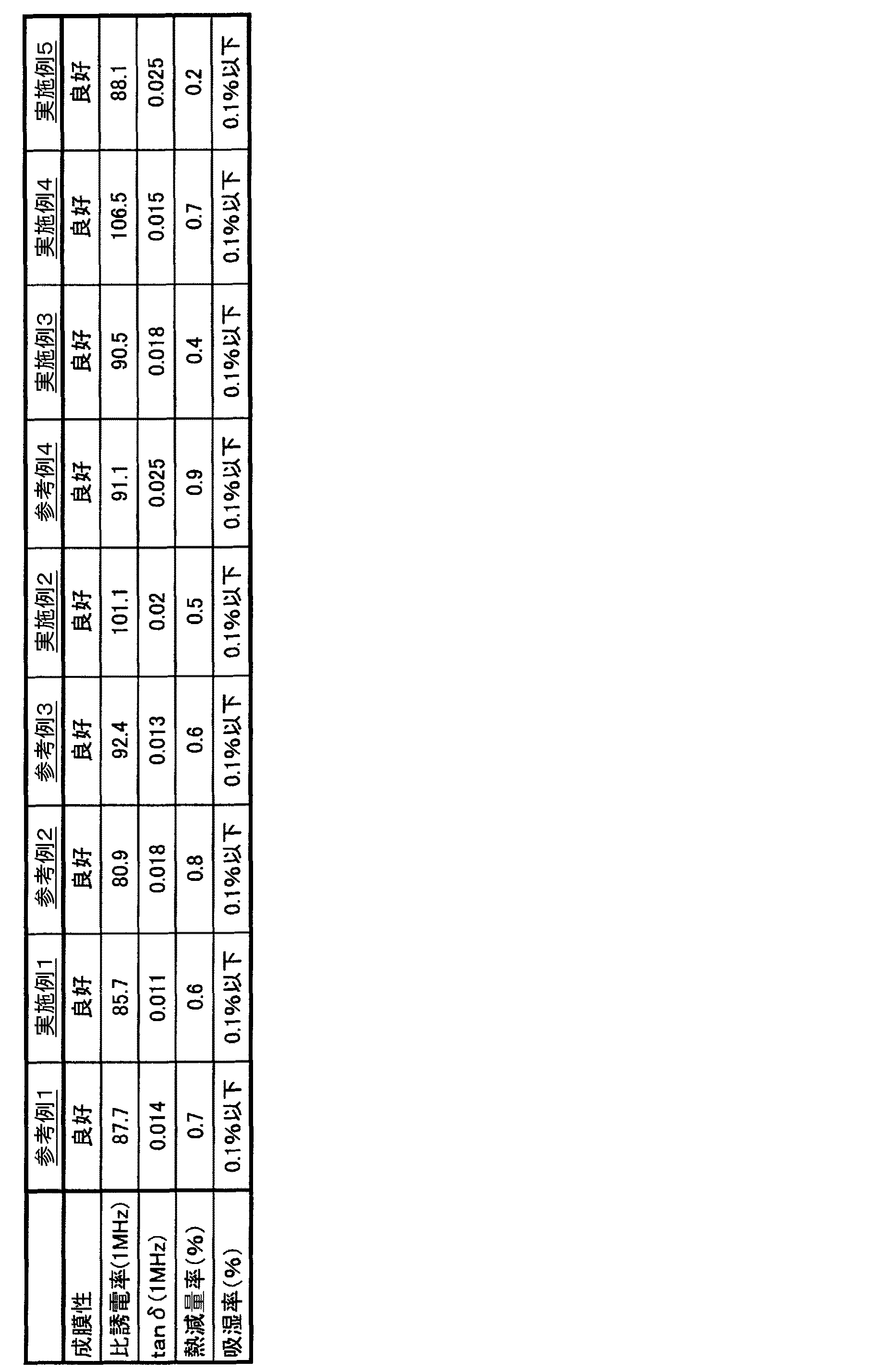
実施例1〜5、参考例1〜4、比較例1〜3
本発明にかかる複合誘電体用液状組成物として、表1に記載した配合量でフッ素化芳香族ポリマー、有機溶剤、分散剤、さらに無機誘電体の順に配合して、ケミスターラーにより均一に混合して、液状組成物を得た。また、比較の液状組成物として、表2に記載した配合量で同様に混合して組成物を得た。
次に、あらかじめ白金膜を形成した、ガラス板上にスピンコーターにより上記の組成物を塗布した後、室温で30分間乾燥後、さらに所定温度のオーブン中で乾燥させ、厚み20μmの複合誘電体を得た。さらに、複合誘電体の表面にイオンスパッタにより白金膜を形成して、評価用の複合誘電体を作製した。この複合誘電体を以下の方法により評価した。その結果を表3および表4に記載した。
Examples 1 to 5, Reference Examples 1 to 4, Comparative Examples 1 to 3
As a liquid composition for a composite dielectric according to the present invention, a fluorinated aromatic polymer, an organic solvent, a dispersant, and an inorganic dielectric are blended in the order shown in Table 1 and mixed uniformly by a chemistor. Thus, a liquid composition was obtained. Moreover, it mixed similarly by the compounding quantity described in Table 2 as a comparative liquid composition, and obtained the composition.
Next, after applying the above composition on a glass plate on which a platinum film has been formed in advance, using a spin coater, the composition is dried at room temperature for 30 minutes, and further dried in an oven at a predetermined temperature to obtain a composite dielectric having a thickness of 20 μm. Obtained. Further, a platinum film was formed on the surface of the composite dielectric by ion sputtering to produce a composite dielectric for evaluation. This composite dielectric was evaluated by the following method. The results are shown in Tables 3 and 4.
評価方法
誘電特性
得られた各複合誘電体をインピーダンス・アナライザにより比誘電率および誘電正接を測定した。
(2)耐熱特性
得られた各複合誘電体をサーマルアナライザ(TG−DTA分析)により、300℃までの減量率を測定した。
吸湿特性
得られた各複合誘電体をPCT試験(135℃、3気圧、2時間)を行い、試験後の吸湿率を測定した。 Evaluation method Dielectric properties Each of the obtained composite dielectrics was measured for relative dielectric constant and dielectric loss tangent by an impedance analyzer.
(2) Heat resistance characteristics The weight loss rate up to 300 ° C. was measured for each obtained composite dielectric using a thermal analyzer (TG-DTA analysis).
Hygroscopic properties Each composite dielectric obtained was subjected to a PCT test (135 ° C., 3 atm, 2 hours), and the moisture absorption rate after the test was measured.
![]()
![]()
BaTiO3:平均粒子径500nm、比表面積2.2m2/g
SrTiO3:平均粒子径1.5μm、比表面積7m2/g
BYK W9010:商品名、ビックケミージャパン社製BaTiO 3 : average particle diameter 500 nm, specific surface area 2.2 m 2 / g
SrTiO 3 : average particle diameter 1.5 μm, specific surface area 7 m 2 / g
BYK W9010: Product name, manufactured by Big Chemie Japan
PTFE:ポリテトラフルオロエチレンディスパージョン、固形分濃度60%、ダイキン工業社製、
フッ素樹脂
YD−127:商品名、東都化成社製、ビスフェノールA型エポキシ樹脂
MT−500:商品名、新日本理化社製、メチルテトラヒドロ無水フタル酸PTFE: polytetrafluoroethylene dispersion, solid content concentration 60%, manufactured by Daikin Industries,
Fluororesin YD-127: trade name, manufactured by Tohto Kasei Co., Ltd., bisphenol A type epoxy resin MT-500: trade name, manufactured by Shin Nippon Rika Co., Ltd., methyltetrahydrophthalic anhydride
表3から明らかなように、実施例1〜5、参考例1〜4の複合誘電体用液状組成物から得られた複合誘電体は有機ポリマーへの無機誘電体の分散性に優れ、良好な成膜性を有している上、高い比誘電率と低い誘電正接を有する。また、耐熱性が高く、吸湿性が低いといった、電気回路基板用材料として理想的な性能を示している。ここで、誘電正接(tanδ)とは誘電体中の位相差δ(90°−θ)の正接のことであり、誘電正接が大きいほど電気エネルギーが熱エネルギーとして消費される量が多くなり、誘電体の発熱によるエネルギーロスと誘電体そのものの熱劣化が起こりやすくなる。 As is apparent from Table 3, the composite dielectrics obtained from the liquid compositions for composite dielectrics of Examples 1 to 5 and Reference Examples 1 to 4 have excellent dispersibility of the inorganic dielectric in the organic polymer and are good. In addition to having film-forming properties, it has a high relative dielectric constant and a low dielectric loss tangent. In addition, it shows ideal performance as a material for electric circuit boards, such as high heat resistance and low hygroscopicity. Here, the dielectric loss tangent (tan δ) is a tangent of the phase difference δ (90 ° −θ) in the dielectric, and the larger the dielectric tangent, the greater the amount of electric energy consumed as heat energy. Energy loss due to body heat generation and thermal degradation of the dielectric itself are likely to occur.
一方、表4に示すように、比較例1のフッ素樹脂では、比誘電率を上げるために無機誘電体を高配合すると成膜性等の成形性が低下してしまう。また、比較例2および3のエポキシ樹脂では無機誘電体を高配合しにくい上、樹脂自体の耐熱性が低く、吸湿性が高いため、複合誘電体としての性能も低いものとなる。
ここでいう成膜性が悪いとは、複合誘電体用液状組成物の粘度が不適当、分散状態が悪い等で膜化できない又は成形した膜がもろい等で膜状態を維持できないことを指す。On the other hand, as shown in Table 4, in the fluororesin of Comparative Example 1, when an inorganic dielectric is highly blended in order to increase the relative dielectric constant, moldability such as film formability is lowered. Further, in the epoxy resins of Comparative Examples 2 and 3, it is difficult to add a high amount of inorganic dielectric, and since the resin itself has low heat resistance and high hygroscopicity, the performance as a composite dielectric is also low.
The term “poor film formability” as used herein means that the liquid composition for composite dielectric cannot be formed because the viscosity of the liquid composition for composite dielectric is inappropriate and the dispersion state is bad, or the film state cannot be maintained because the formed film is brittle.
本発明の複合誘電体用液状組成物より得られた複合誘電体は高い誘電率と低い誘電正接、さらに、高い耐熱性を有するものとなるため、EPD(Embedded Passive Device Techinology)用途をはじめとする各種バイパスコンデンサー、充電素子、微分素子、終端負荷素子、フィルター、アンテナ等の電子素子として有効に利用することができる。The composite dielectric obtained from the liquid composition for composite dielectric of the present invention has a high dielectric constant, a low dielectric loss tangent, and a high heat resistance, so that it is used for EPD (Embedded Passive Device Technology). It can be effectively used as various bypass capacitors, charging elements, differentiating elements, terminal load elements, filters, antennas and other electronic elements.
Claims (6)
該無機誘電体が、該フッ素化芳香族ポリマー100質量部に対して、700〜2000質量部の範囲にあり、
該フッ素化芳香族ポリマーは、20℃〜80℃の反応温度で合成されたものであって、下記一般式(1)で表される繰り返し単位を含むものであり、該一般式(1)で表される繰り返し単位のうち少なくとも1つが9,9−ビス(4−ヒドロキシフェニル)フルオレン骨格を含む
ことを特徴とする複合誘電体用液状組成物。
構造式群(2)
構造式(4−6)
構造式群(3)
The inorganic dielectric is in the range of 700 to 2000 parts by mass with respect to 100 parts by mass of the fluorinated aromatic polymer,
The fluorinated aromatic polymer, which has been synthesized at a reaction temperature of 20 ° C. to 80 ° C., a repeating unit represented by the following general formula (1) and Dressings containing, the general formula (1) A liquid composition for a composite dielectric, wherein at least one of the represented repeating units includes a 9,9-bis (4-hydroxyphenyl) fluorene skeleton .
Structural formula group (2)
Structural formula (4-6)
Structural formula group (3)
ことを特徴とする請求項1に記載の複合誘電体用液状組成物。2. The composite dielectric according to claim 1 , wherein in the fluorinated aromatic polymer, X in the general formula (1) is a diphenyl ether chain, a bisphenol A chain, a bisphenol F chain, or a fluorene chain. Liquid composition.
ことを特徴とする請求項1又は2に記載の複合誘電体用液状組成物。The fluorinated aromatic polymer has a number average molecular weight (Mn) of composite dielectric for liquid composition according to claim 1 or 2, characterized in that it is 10,000 to 200,000.
Applications Claiming Priority (3)
| Application Number | Priority Date | Filing Date | Title |
|---|---|---|---|
| JP2003338973 | 2003-09-30 | ||
| JP2003338973 | 2003-09-30 | ||
| PCT/JP2004/013764 WO2005033209A1 (en) | 2003-09-30 | 2004-09-21 | Resin composition for composite dielectric body, composite dielectric body, and electrical circuit board using such composite dielectric body |
Publications (2)
| Publication Number | Publication Date |
|---|---|
| JPWO2005033209A1 JPWO2005033209A1 (en) | 2006-12-14 |
| JP4601552B2 true JP4601552B2 (en) | 2010-12-22 |
Family
ID=34419140
Family Applications (1)
| Application Number | Title | Priority Date | Filing Date |
|---|---|---|---|
| JP2005514395A Expired - Fee Related JP4601552B2 (en) | 2003-09-30 | 2004-09-21 | Resin composition for composite dielectric, composite dielectric, and electric circuit board using the dielectric |
Country Status (7)
| Country | Link |
|---|---|
| US (1) | US7632884B2 (en) |
| EP (1) | EP1669412A1 (en) |
| JP (1) | JP4601552B2 (en) |
| KR (1) | KR100884511B1 (en) |
| CN (1) | CN100582167C (en) |
| TW (1) | TW200513494A (en) |
| WO (1) | WO2005033209A1 (en) |
Cited By (1)
| Publication number | Priority date | Publication date | Assignee | Title |
|---|---|---|---|---|
| KR101452594B1 (en) | 2012-12-26 | 2014-10-21 | 주식회사 두산 | Resin compositions and metal foil laminate comprising the resin composition |
Families Citing this family (13)
| Publication number | Priority date | Publication date | Assignee | Title |
|---|---|---|---|---|
| WO2005033209A1 (en) * | 2003-09-30 | 2005-04-14 | Nippon Shokubai Co., Ltd. | Resin composition for composite dielectric body, composite dielectric body, and electrical circuit board using such composite dielectric body |
| US7521705B2 (en) | 2005-08-15 | 2009-04-21 | Micron Technology, Inc. | Reproducible resistance variable insulating memory devices having a shaped bottom electrode |
| US8414962B2 (en) | 2005-10-28 | 2013-04-09 | The Penn State Research Foundation | Microcontact printed thin film capacitors |
| JP5595629B2 (en) * | 2005-12-13 | 2014-09-24 | 東レ株式会社 | Dielectric resin composition and molded product obtained therefrom |
| KR101051404B1 (en) * | 2006-04-05 | 2011-07-22 | 가부시키가이샤 무라타 세이사쿠쇼 | Manufacturing method of multilayer ceramic electronic component and multilayer ceramic electronic component |
| JP4991185B2 (en) * | 2006-06-05 | 2012-08-01 | 株式会社日本触媒 | Polyarylsulfone polymer and process for producing the same |
| JP5470788B2 (en) * | 2008-09-22 | 2014-04-16 | セイコーエプソン株式会社 | ORGANIC SEMICONDUCTOR DEVICE, ORGANIC SEMICONDUCTOR DEVICE MANUFACTURING METHOD, ELECTRONIC DEVICE, AND ELECTRONIC DEVICE |
| JP5470787B2 (en) * | 2008-09-22 | 2014-04-16 | セイコーエプソン株式会社 | ORGANIC SEMICONDUCTOR DEVICE, ORGANIC SEMICONDUCTOR DEVICE MANUFACTURING METHOD, ELECTRONIC DEVICE, AND ELECTRONIC DEVICE |
| JP5708160B2 (en) * | 2011-04-04 | 2015-04-30 | Jsr株式会社 | Resin substrate for high frequency circuit board and high frequency circuit board |
| KR102059198B1 (en) * | 2012-03-22 | 2019-12-24 | 가부시키가이샤 닛폰 쇼쿠바이 | Light selective transmission filter, resin sheet, and solid-state image sensing device |
| US9809720B2 (en) * | 2015-07-06 | 2017-11-07 | University Of Massachusetts | Ferroelectric nanocomposite based dielectric inks for reconfigurable RF and microwave applications |
| US10839992B1 (en) | 2019-05-17 | 2020-11-17 | Raytheon Company | Thick film resistors having customizable resistances and methods of manufacture |
| CN112574521B (en) * | 2020-12-09 | 2022-04-26 | 广东生益科技股份有限公司 | Fluorine-containing resin composition, resin glue solution containing same, fluorine-containing medium sheet, laminated board, copper-clad plate and printed circuit board |
Family Cites Families (28)
| Publication number | Priority date | Publication date | Assignee | Title |
|---|---|---|---|---|
| US2764718A (en) * | 1951-12-28 | 1956-09-25 | Sprague Electric Co | Electrical condensers |
| US4518737A (en) * | 1978-12-26 | 1985-05-21 | Rogers Corporation | Dielectric material and method of making the dielectric material |
| JPH02225358A (en) * | 1989-02-23 | 1990-09-07 | Matsushita Electric Works Ltd | Complex dielectric material |
| US5114780A (en) * | 1990-04-17 | 1992-05-19 | Raychem Corporation | Electronic articles containing a fluorinated poly(arylene ether) dielectric |
| EP0505438A1 (en) | 1989-12-08 | 1992-09-30 | AlliedSignal Inc. | Electronic articles containing a fluorinated poly(arylene ether) dielectric |
| US5275878A (en) * | 1990-02-06 | 1994-01-04 | Matsushita Electric Works, Ltd. | Composite dielectric and printed-circuit use substrate utilizing the same |
| JP2802173B2 (en) * | 1990-02-06 | 1998-09-24 | 松下電工株式会社 | Composite dielectric |
| JP3089032B2 (en) * | 1990-04-17 | 2000-09-18 | アライド・シグナル・インコーポレイテツド | Fluorine poly (arylene ether) |
| US5115082A (en) * | 1990-04-17 | 1992-05-19 | Raychem Corporation | Fluorinated poly(arylene ether) |
| WO1992018213A1 (en) * | 1991-04-12 | 1992-10-29 | E.I. Du Pont De Nemours And Company | High dielectric constant flexible ceramic composite |
| JP2617639B2 (en) * | 1991-11-06 | 1997-06-04 | 松下電工株式会社 | Composite dielectric and circuit board |
| US6207764B1 (en) * | 1995-04-26 | 2001-03-27 | Monsanto Company | Halogenated elastomer compositions |
| US5739193A (en) * | 1996-05-07 | 1998-04-14 | Hoechst Celanese Corp. | Polymeric compositions having a temperature-stable dielectric constant |
| US6599631B2 (en) * | 2001-01-26 | 2003-07-29 | Nanogram Corporation | Polymer-inorganic particle composites |
| JPH11260148A (en) | 1998-03-13 | 1999-09-24 | Hitachi Ltd | Thin film dielectric, multilayer wiring board using the same, and method of manufacturing the same |
| JP4044236B2 (en) * | 1999-03-11 | 2008-02-06 | 株式会社東芝 | Manufacturing method of semiconductor device |
| TWI256959B (en) * | 2000-07-31 | 2006-06-21 | Sumitomo Chemical Co | Aromatic liquid-crystalline polyester solution composition |
| JP4543518B2 (en) * | 2000-08-11 | 2010-09-15 | 住友化学株式会社 | Dielectric paste and dielectric film |
| KR100399018B1 (en) * | 2000-12-19 | 2003-09-19 | 광주과학기술원 | Poly(arylene ether sulfide) and poly(arylene ether sulfone) for optical device and method for preparing the same |
| US6797345B2 (en) * | 2001-04-27 | 2004-09-28 | Sumitomo Chemical Company, Limited | Aromatic liquid-crystalline polyester metal laminate |
| JP2002344100A (en) * | 2001-05-21 | 2002-11-29 | Sumitomo Electric Ind Ltd | Dielectric material for substrate and method of manufacturing the same |
| US6706136B2 (en) * | 2001-10-16 | 2004-03-16 | Toyo Boseki Kabushiki Kaisha | Resin composition for high-frequency bonding |
| JP4273739B2 (en) | 2001-10-16 | 2009-06-03 | 東洋紡績株式会社 | RESIN COMPOSITION FOR DIELECTRIC HEAT-ADJUSTING, HOT-MELT ADHESIVE, ADHESIVE METHOD FOR ADHESIVE MATERIAL, ADHESIVE RESIN COMPOSITION AND ADHESIVE COMPOSITE USED AS A HOT-MELT ADHESIVE ADHESIVE |
| JP2003138026A (en) * | 2001-11-05 | 2003-05-14 | Nippon Shokubai Co Ltd | Resin composition and molded article |
| CA2487649C (en) * | 2002-05-28 | 2009-09-01 | National Research Council Of Canada | Techniques for the preparation of highly fluorinated polyethers |
| US7164197B2 (en) * | 2003-06-19 | 2007-01-16 | 3M Innovative Properties Company | Dielectric composite material |
| WO2005033209A1 (en) * | 2003-09-30 | 2005-04-14 | Nippon Shokubai Co., Ltd. | Resin composition for composite dielectric body, composite dielectric body, and electrical circuit board using such composite dielectric body |
| JP2009016169A (en) * | 2007-07-04 | 2009-01-22 | Nippon Shokubai Co Ltd | Resin composition for compound dielectric and compound dielectric, and electric circuit board using this dielectric |
-
2004
- 2004-09-21 WO PCT/JP2004/013764 patent/WO2005033209A1/en not_active Ceased
- 2004-09-21 KR KR1020067006140A patent/KR100884511B1/en not_active Expired - Fee Related
- 2004-09-21 JP JP2005514395A patent/JP4601552B2/en not_active Expired - Fee Related
- 2004-09-21 CN CN200480028531A patent/CN100582167C/en not_active Expired - Fee Related
- 2004-09-21 EP EP04787947A patent/EP1669412A1/en not_active Withdrawn
- 2004-09-28 US US10/950,454 patent/US7632884B2/en not_active Expired - Fee Related
- 2004-09-29 TW TW093129323A patent/TW200513494A/en not_active IP Right Cessation
Cited By (1)
| Publication number | Priority date | Publication date | Assignee | Title |
|---|---|---|---|---|
| KR101452594B1 (en) | 2012-12-26 | 2014-10-21 | 주식회사 두산 | Resin compositions and metal foil laminate comprising the resin composition |
Also Published As
| Publication number | Publication date |
|---|---|
| KR20060097719A (en) | 2006-09-14 |
| JPWO2005033209A1 (en) | 2006-12-14 |
| CN1860184A (en) | 2006-11-08 |
| TWI304830B (en) | 2009-01-01 |
| US7632884B2 (en) | 2009-12-15 |
| US20050101714A1 (en) | 2005-05-12 |
| EP1669412A1 (en) | 2006-06-14 |
| TW200513494A (en) | 2005-04-16 |
| CN100582167C (en) | 2010-01-20 |
| WO2005033209A1 (en) | 2005-04-14 |
| KR100884511B1 (en) | 2009-02-18 |
Similar Documents
| Publication | Publication Date | Title |
|---|---|---|
| JP4601552B2 (en) | Resin composition for composite dielectric, composite dielectric, and electric circuit board using the dielectric | |
| EP1387367B1 (en) | Composite particle for dielectrics, ultramicroparticulate composite resin particle, composition for forming dielectrics and use thereof | |
| TWI778307B (en) | Resin composition, prepreg including the same, laminated plate including the same, resin-coated metal foil including the same | |
| US20050031849A1 (en) | Composite dielectric, composite dielectric sheet, composite dielectric paste, metal-layered composite dielectric, wiring board and multilayer wiring board | |
| KR20020011086A (en) | Aromatic liquid-crystalline polyester solution composition | |
| KR20110108782A (en) | Thermosetting composition and printed circuit board using the same | |
| KR102871645B1 (en) | Metal-clad laminate and circuit board | |
| CN111344351A (en) | Resin composition, copper foil with resin, dielectric layer, copper clad laminate, capacitor element, and printed circuit board with built-in capacitor | |
| CN115023348B (en) | Resin laminate, dielectric layer, metal foil with resin, capacitor element, and capacitor built-in printed circuit board | |
| KR101107847B1 (en) | Crystalline encapsulants | |
| JP2006019621A (en) | Polymer ceramic composite materials for capacitors, multilayer wiring boards and module boards | |
| KR102226117B1 (en) | Circuit board structure and composite for forming insulating substrates | |
| JP2009096934A (en) | Composition for composite dielectric, composite dielectric and electric circuit substrate containing the composite dielectric | |
| JP2009016169A (en) | Resin composition for compound dielectric and compound dielectric, and electric circuit board using this dielectric | |
| JP2003105205A (en) | High permittivity composite material, high permittivity film, laminated board with metal foil and printed wiring board | |
| CN118667157A (en) | Polyimide precursor and polyimide prepared therefrom | |
| JP2012055095A (en) | Polymer composition for electret material and electret material | |
| JP4045621B2 (en) | Electrical insulating material containing fluorine-containing polyimide resin and electronic component using the same | |
| JP2003119379A (en) | Resin composition and utilization thereof | |
| JP2004315653A (en) | Resin composition and its use | |
| TWI920055B (en) | Resin composites, dielectric layers, resin-coated metal foils, capacitor components, and printed circuit boards containing built-in capacitors. | |
| JP2005105193A (en) | Dendritic polymer and polymer material of high dielectric constant | |
| US12598697B2 (en) | Circuit board and multilayer circuit board | |
| JP2005109316A (en) | Inorganic material of high dielectric constant, and high dielectric constant composite material using the same | |
| JPS5811899B2 (en) | polyamideimide composition |
Legal Events
| Date | Code | Title | Description |
|---|---|---|---|
| A131 | Notification of reasons for refusal |
Free format text: JAPANESE INTERMEDIATE CODE: A131 Effective date: 20090512 |
|
| A521 | Request for written amendment filed |
Free format text: JAPANESE INTERMEDIATE CODE: A523 Effective date: 20090709 |
|
| RD02 | Notification of acceptance of power of attorney |
Free format text: JAPANESE INTERMEDIATE CODE: A7422 Effective date: 20090709 |
|
| A02 | Decision of refusal |
Free format text: JAPANESE INTERMEDIATE CODE: A02 Effective date: 20100223 |
|
| A521 | Request for written amendment filed |
Free format text: JAPANESE INTERMEDIATE CODE: A523 Effective date: 20100524 |
|
| A911 | Transfer to examiner for re-examination before appeal (zenchi) |
Free format text: JAPANESE INTERMEDIATE CODE: A911 Effective date: 20100607 |
|
| A131 | Notification of reasons for refusal |
Free format text: JAPANESE INTERMEDIATE CODE: A131 Effective date: 20100706 |
|
| A521 | Request for written amendment filed |
Free format text: JAPANESE INTERMEDIATE CODE: A523 Effective date: 20100903 |
|
| TRDD | Decision of grant or rejection written | ||
| A01 | Written decision to grant a patent or to grant a registration (utility model) |
Free format text: JAPANESE INTERMEDIATE CODE: A01 Effective date: 20100928 |
|
| A01 | Written decision to grant a patent or to grant a registration (utility model) |
Free format text: JAPANESE INTERMEDIATE CODE: A01 |
|
| A61 | First payment of annual fees (during grant procedure) |
Free format text: JAPANESE INTERMEDIATE CODE: A61 Effective date: 20100928 |
|
| FPAY | Renewal fee payment (event date is renewal date of database) |
Free format text: PAYMENT UNTIL: 20131008 Year of fee payment: 3 |
|
| R150 | Certificate of patent or registration of utility model |
Free format text: JAPANESE INTERMEDIATE CODE: R150 |
|
| LAPS | Cancellation because of no payment of annual fees |