JP4589853B2 - Substrate transport system and substrate transport method - Google Patents
Substrate transport system and substrate transport method Download PDFInfo
- Publication number
- JP4589853B2 JP4589853B2 JP2005276441A JP2005276441A JP4589853B2 JP 4589853 B2 JP4589853 B2 JP 4589853B2 JP 2005276441 A JP2005276441 A JP 2005276441A JP 2005276441 A JP2005276441 A JP 2005276441A JP 4589853 B2 JP4589853 B2 JP 4589853B2
- Authority
- JP
- Japan
- Prior art keywords
- substrate
- transfer
- wafer
- transport
- processing apparatus
- Prior art date
- Legal status (The legal status is an assumption and is not a legal conclusion. Google has not performed a legal analysis and makes no representation as to the accuracy of the status listed.)
- Expired - Fee Related
Links
Images


Classifications
-
- H—ELECTRICITY
- H01—ELECTRIC ELEMENTS
- H01L—SEMICONDUCTOR DEVICES NOT COVERED BY CLASS H10
- H01L21/00—Processes or apparatus adapted for the manufacture or treatment of semiconductor or solid state devices or of parts thereof
- H01L21/67—Apparatus specially adapted for handling semiconductor or electric solid state devices during manufacture or treatment thereof; Apparatus specially adapted for handling wafers during manufacture or treatment of semiconductor or electric solid state devices or components ; Apparatus not specifically provided for elsewhere
- H01L21/67005—Apparatus not specifically provided for elsewhere
- H01L21/67011—Apparatus for manufacture or treatment
- H01L21/67155—Apparatus for manufacturing or treating in a plurality of work-stations
- H01L21/67196—Apparatus for manufacturing or treating in a plurality of work-stations characterized by the construction of the transfer chamber
-
- H—ELECTRICITY
- H01—ELECTRIC ELEMENTS
- H01L—SEMICONDUCTOR DEVICES NOT COVERED BY CLASS H10
- H01L21/00—Processes or apparatus adapted for the manufacture or treatment of semiconductor or solid state devices or of parts thereof
- H01L21/67—Apparatus specially adapted for handling semiconductor or electric solid state devices during manufacture or treatment thereof; Apparatus specially adapted for handling wafers during manufacture or treatment of semiconductor or electric solid state devices or components ; Apparatus not specifically provided for elsewhere
- H01L21/673—Apparatus specially adapted for handling semiconductor or electric solid state devices during manufacture or treatment thereof; Apparatus specially adapted for handling wafers during manufacture or treatment of semiconductor or electric solid state devices or components ; Apparatus not specifically provided for elsewhere using specially adapted carriers or holders; Fixing the workpieces on such carriers or holders
- H01L21/6732—Vertical carrier comprising wall type elements whereby the substrates are horizontally supported, e.g. comprising sidewalls
-
- H—ELECTRICITY
- H01—ELECTRIC ELEMENTS
- H01L—SEMICONDUCTOR DEVICES NOT COVERED BY CLASS H10
- H01L21/00—Processes or apparatus adapted for the manufacture or treatment of semiconductor or solid state devices or of parts thereof
- H01L21/67—Apparatus specially adapted for handling semiconductor or electric solid state devices during manufacture or treatment thereof; Apparatus specially adapted for handling wafers during manufacture or treatment of semiconductor or electric solid state devices or components ; Apparatus not specifically provided for elsewhere
- H01L21/67005—Apparatus not specifically provided for elsewhere
- H01L21/67011—Apparatus for manufacture or treatment
- H01L21/67155—Apparatus for manufacturing or treating in a plurality of work-stations
- H01L21/67161—Apparatus for manufacturing or treating in a plurality of work-stations characterized by the layout of the process chambers
- H01L21/67173—Apparatus for manufacturing or treating in a plurality of work-stations characterized by the layout of the process chambers in-line arrangement
-
- H—ELECTRICITY
- H01—ELECTRIC ELEMENTS
- H01L—SEMICONDUCTOR DEVICES NOT COVERED BY CLASS H10
- H01L21/00—Processes or apparatus adapted for the manufacture or treatment of semiconductor or solid state devices or of parts thereof
- H01L21/67—Apparatus specially adapted for handling semiconductor or electric solid state devices during manufacture or treatment thereof; Apparatus specially adapted for handling wafers during manufacture or treatment of semiconductor or electric solid state devices or components ; Apparatus not specifically provided for elsewhere
- H01L21/67005—Apparatus not specifically provided for elsewhere
- H01L21/67242—Apparatus for monitoring, sorting or marking
- H01L21/67276—Production flow monitoring, e.g. for increasing throughput
-
- H—ELECTRICITY
- H01—ELECTRIC ELEMENTS
- H01L—SEMICONDUCTOR DEVICES NOT COVERED BY CLASS H10
- H01L21/00—Processes or apparatus adapted for the manufacture or treatment of semiconductor or solid state devices or of parts thereof
- H01L21/67—Apparatus specially adapted for handling semiconductor or electric solid state devices during manufacture or treatment thereof; Apparatus specially adapted for handling wafers during manufacture or treatment of semiconductor or electric solid state devices or components ; Apparatus not specifically provided for elsewhere
- H01L21/677—Apparatus specially adapted for handling semiconductor or electric solid state devices during manufacture or treatment thereof; Apparatus specially adapted for handling wafers during manufacture or treatment of semiconductor or electric solid state devices or components ; Apparatus not specifically provided for elsewhere for conveying, e.g. between different workstations
- H01L21/67703—Apparatus specially adapted for handling semiconductor or electric solid state devices during manufacture or treatment thereof; Apparatus specially adapted for handling wafers during manufacture or treatment of semiconductor or electric solid state devices or components ; Apparatus not specifically provided for elsewhere for conveying, e.g. between different workstations between different workstations
- H01L21/6773—Conveying cassettes, containers or carriers
-
- H—ELECTRICITY
- H01—ELECTRIC ELEMENTS
- H01L—SEMICONDUCTOR DEVICES NOT COVERED BY CLASS H10
- H01L21/00—Processes or apparatus adapted for the manufacture or treatment of semiconductor or solid state devices or of parts thereof
- H01L21/67—Apparatus specially adapted for handling semiconductor or electric solid state devices during manufacture or treatment thereof; Apparatus specially adapted for handling wafers during manufacture or treatment of semiconductor or electric solid state devices or components ; Apparatus not specifically provided for elsewhere
- H01L21/677—Apparatus specially adapted for handling semiconductor or electric solid state devices during manufacture or treatment thereof; Apparatus specially adapted for handling wafers during manufacture or treatment of semiconductor or electric solid state devices or components ; Apparatus not specifically provided for elsewhere for conveying, e.g. between different workstations
- H01L21/67703—Apparatus specially adapted for handling semiconductor or electric solid state devices during manufacture or treatment thereof; Apparatus specially adapted for handling wafers during manufacture or treatment of semiconductor or electric solid state devices or components ; Apparatus not specifically provided for elsewhere for conveying, e.g. between different workstations between different workstations
- H01L21/67736—Loading to or unloading from a conveyor
-
- Y—GENERAL TAGGING OF NEW TECHNOLOGICAL DEVELOPMENTS; GENERAL TAGGING OF CROSS-SECTIONAL TECHNOLOGIES SPANNING OVER SEVERAL SECTIONS OF THE IPC; TECHNICAL SUBJECTS COVERED BY FORMER USPC CROSS-REFERENCE ART COLLECTIONS [XRACs] AND DIGESTS
- Y10—TECHNICAL SUBJECTS COVERED BY FORMER USPC
- Y10S—TECHNICAL SUBJECTS COVERED BY FORMER USPC CROSS-REFERENCE ART COLLECTIONS [XRACs] AND DIGESTS
- Y10S414/00—Material or article handling
- Y10S414/135—Associated with semiconductor wafer handling
- Y10S414/14—Wafer cassette transporting
Landscapes
- Engineering & Computer Science (AREA)
- Physics & Mathematics (AREA)
- Condensed Matter Physics & Semiconductors (AREA)
- General Physics & Mathematics (AREA)
- Manufacturing & Machinery (AREA)
- Computer Hardware Design (AREA)
- Microelectronics & Electronic Packaging (AREA)
- Power Engineering (AREA)
- Automation & Control Theory (AREA)
- Container, Conveyance, Adherence, Positioning, Of Wafer (AREA)
Description
本発明は、基板搬送システム及び基板搬送方法に関し、特に、基板を枚葉で搬送する基板搬送システム及び基板搬送方法に関する。 The present invention relates to a substrate transport system及 beauty substrate transfer method, particularly to a substrate transfer system and the substrate transfer method for transferring a substrate in a single wafer.
基板としてのウエハに複数の工程からなる処理を施す基板処理システムとしての基盤搬送システムは、未処理又は処理済みのウエハをストックするストッカと、各工程に対応した複数の基板処理装置と、ストッカ及び各基板処理装置の間においてウエハを搬送する基板搬送車としてのRGV(Rail Guided Vehicle)とを備える。 A substrate transfer system as a substrate processing system for performing processing consisting of a plurality of processes on a wafer as a substrate includes a stocker for stocking unprocessed or processed wafers, a plurality of substrate processing apparatuses corresponding to each process, a stocker, RGV (Rail Guided Vehicle) as a substrate transfer vehicle for transferring wafers between the substrate processing apparatuses is provided.
従来はウエハの口径が小さく、1枚のウエハに対する各工程の所要時間が短かったため、搬送効率向上の観点からRGVはストッカ及び各基板処理装置の間において複数のウエハ、例えば25枚のウエハを収容するキャリアを搬送し、該キャリアを各基板処理装置に搬入していた。 Conventionally, since the diameter of the wafer is small and the time required for each process for one wafer is short, the RGV accommodates a plurality of wafers, for example, 25 wafers, between the stocker and each substrate processing apparatus from the viewpoint of improving the transfer efficiency. The carrier to be carried was transported, and the carrier was carried into each substrate processing apparatus.
ところが、近年、ウエハの大口径化に伴って1枚のウエハに対する各工程の所要時間が長くなったため、各基板処理装置にウエハを1枚ずつ枚葉で搬入する基板搬送システム(以下、「枚葉搬送システム」という。)が主流となっている。この基板搬送システムにおけるRGVは、該RGVが備える搬送アーム機構によってウエハを枚葉単位でストッカから受け取り、該受け取ったウエハをRGVが備えるバッファ内に収容して搬送する(例えば、特許文献1参照。)。また、RGVは、基板処理装置にウエハを搬入するとき、バッファ内に収容されたウエハを搬送アーム機構によって取り出して基板処理装置に搬入する。
しかしながら、上述した枚葉搬送システムでは、所定の時間を要する、RGVにおけるウエハのバッファへの収容及びバッファからの取り出しの回数が多いため、枚葉搬送システムにおけるウエハの搬送効率を向上することができないという問題がある。さらに、近年、処理技術の向上に伴い各工程の所要時間が短くなっているため、RGVにおけるウエハのバッファへの収容及びバッファからの取り出しが枚葉搬送システムにおけるウエハの搬送効率向上のボトルネックとなっている。 However, in the single wafer transfer system described above, the wafer transfer efficiency in the single wafer transfer system cannot be improved because the RGV requires a large number of times the wafer is accommodated in and removed from the buffer. There is a problem. Furthermore, in recent years, the time required for each process has been shortened along with the improvement of processing technology. Therefore, the storage and removal from the buffer in the RGV is a bottleneck for improving the wafer transfer efficiency in the single wafer transfer system. It has become.
本発明の目的は、基板の搬送効率を向上させることができる基板搬送システム及び基板搬送方法を提供することにある。 An object of the present invention is to provide a substrate transfer system及 beauty substrate transfer method capable Rukoto improve the transport efficiency of the substrate.
上記目的を達成するために、請求項1記載の基板搬送システムは、基板を保管する基板保管装置と、前記基板に所定の処理を施す少なくとも1つの基板処理装置と、前記基板保管装置と前記基板処理装置との間を移動して前記基板を搬送する基板搬送装置と、を備え、前記基板搬送装置は前記基板を保持し、前記基板保管装置又は前記基板処理装置から前記基板を搬出し、且つ、前記基板保管装置又は前記基板処理装置へ前記基板を搬入するための少なくとも1つの基板搬送手段を有する基板搬送システムであって、前記基板処理装置は複数の前記基板を受け渡す基板受け渡し部を有し、前記基板受け渡し部は前記基板を収容する複数の基板収容手段を有し、前記基板収容手段はそれぞれ1枚の前記基板を収容し、前記基板搬送装置は複数の前記基板搬送手段を備え、前記複数の基板搬送手段の少なくとも1つは複数の前記基板を保持すると共に、他の前記基板搬送手段のうち少なくとも1つが1枚の前記基板を保持し、前記基板受け渡し部における前記基板を収容していない前記基板収容手段の数に応じて、前記基板受け渡し部に前記基板を受け渡す基板搬送手段が前記複数の基板搬送手段から選択され、前記基板搬送装置全体が前記基板搬送手段に前記基板を保持させたまま移動可能であることを特徴とする。
In order to achieve the above object, a substrate transfer system according to
請求項2記載の基板搬送システムは、請求項1記載の基板搬送システムにおいて、前記基板搬送手段は前記基板を載置する搬送アームであることを特徴とする。 A substrate transfer system according to a second aspect of the present invention is the substrate transfer system according to the first aspect , wherein the substrate transfer means is a transfer arm on which the substrate is placed.
請求項3記載の基板搬送システムは、請求項1又は2記載の基板搬送システムにおいて、前記基板搬送システムは、複数の前記基板処理装置を備え、前記基板搬送装置は前記複数の基板処理装置の間を移動することを特徴とする。
Substrate transfer system according to
請求項4記載の基板搬送システムは、請求項1記載の基板搬送システムにおいて、前記基板搬送手段による前記基板の搬送経路を規定する複数の搬送命令を組み合わせて、前記基板の搬送シーケンスを設定する制御装置を備え、前記制御装置は、前記複数の搬送命令のうち少なくとも1つが規定する搬送経路に、前記基板搬送手段が前記基板を保持したまま動作を中断する動作中断位置を設定することを特徴とする。
4. The substrate transfer system according to
請求項5記載の基板搬送システムは、請求項4記載の基板搬送システムにおいて、前記基板搬送装置は複数の前記基板搬送手段を有し、前記制御装置は前記複数の基板搬送手段による前記基板の搬送を連続的に行うか又は搬送経路が互いに異なる前記搬送シーケンスを設定することを特徴とする。
Substrate transfer system according to
請求項6記載の基板搬送システムは、請求項5記載の基板搬送システムにおいて、前記搬送シーケンスでは、前記複数の基板搬送手段のうち少なくとも1つが前記基板を前記基板保管装置又は前記基板処理装置へ搬入すると共に、他の前記基板搬送手段のうち少なくとも1つが前記基板を前記基板保管装置又は前記基板処理装置から搬出することを特徴とする。
Substrate transfer system according to
請求項7記載の基板搬送システムは、請求項6記載の基板搬送システムにおいて、前記基板保管装置は複数の前記基板を受け渡す他の基板受け渡し部を有することを特徴とする。 A substrate transfer system according to a seventh aspect is the substrate transfer system according to the sixth aspect , wherein the substrate storage device includes another substrate transfer unit that transfers a plurality of the substrates.
請求項8記載の基板搬送システムは、請求項1記載の基板搬送システムにおいて、前記基板受け渡し部における前記基板を収容していない前記基板収容手段が1つである場合、前記1枚の前記基板を保持する基板搬送手段が選択されることを特徴とする。
The substrate transfer system according to
上記目的を達成するために、請求項9記載の基板搬送方法は、基板を保管する基板保管装置と、前記基板に所定の処理を施す少なくとも1つの基板処理装置と、前記基板保管装置と前記基板処理装置との間を移動して前記基板を搬送する基板搬送装置と、前記基板の搬送シーケンスを設定する制御装置とを備え、前記基板処理装置は、複数の前記基板を受け渡す基板受け渡し部を有し、前記基板受け渡し部は前記基板を収容する複数の基板収容手段を有し、前記基板収容手段はそれぞれ1枚の前記基板を収容し、前記基板搬送装置は、前記基板を保持し、前記基板保管装置又は前記基板処理装置から前記基板を搬出し、且つ、前記基板保管装置又は前記基板処理装置へ前記基板を搬入する、複数の前記基板搬送手段を備え、前記複数の基板搬送手段の少なくとも1つは複数の前記基板を保持すると共に、他の前記基板搬送手段のうち少なくとも1つが1枚の前記基板を保持する基板搬送システムにおける基板搬送方法であって、前記制御装置が搬送される前記基板の諸元を前記基板処理装置に通知すると共に、前記基板処理装置の状態を問い合わせる状態問い合わせステップと、前記状態を問い合わされた基板処理装置が前記状態を前記制御装置に連絡する状態連絡ステップと、前記制御装置が前記連絡された状態に基づいて前記搬送シーケンスを設定する搬送シーケンス設定ステップと、前記制御装置が前記設定された搬送シーケンスを前記基板搬送装置に通知する搬送シーケンス通知ステップと、前記基板受け渡し部における前記基板を収容していない前記基板収容手段の数に応じて、前記基板受け渡し部に前記基板を受け渡す基板搬送手段が前記複数の基板搬送手段から選択され、前記基板搬送装置全体が前記基板搬送手段に前記基板を保持させたまま移動する移動ステップと、を有することを特徴とする。
In order to achieve the above object, a substrate transport method according to
請求項10記載の基板搬送方法は、請求項9記載の基板搬送方法において、前記基板搬送装置が前記基板処理装置に前記基板受け渡し部の種類を問い合わせる基板受け渡し部種類問い合わせステップと、前記基板処理装置が前記基板受け渡し部の種類を前記基板搬送装置に連絡する基板受け渡し部種類連絡ステップとを更に有することを特徴とする。
Substrate transfer method according to
請求項1記載の基板搬送システムによれば、基板搬送装置が基板搬送手段に基板を保持させたまま移動するので、基板搬送装置において基板をバッファに収容する必要及び基板をバッファから取り出す必要を無くすことができ、もって、基板の搬送効率を向上させることができる。また、基板受け渡し部における基板を収容していない基板収容手段の数に応じて、基板受け渡し部に基板を受け渡す基板搬送手段が、複数の基板を保持する基板搬送手段及び1枚の基板を保持する基板搬送手段から選択されるので、基板を収容していない基板収容手段の数と、基板搬送手段が保持可能な基板の枚数とを整合させることができ、もって、基板の搬送効率を向上させることができる。 According to the substrate transfer system of the first aspect, since the substrate transfer device moves while holding the substrate on the substrate transfer means, it is unnecessary to store the substrate in the buffer and to remove the substrate from the buffer in the substrate transfer device. it can, have, it is Rukoto improve the transport efficiency of the substrate. Further, according to the number of substrate accommodation units that do not accommodate the substrate in the substrate delivery unit, the substrate conveyance unit that delivers the substrate to the substrate delivery unit holds the substrate conveyance unit that holds a plurality of substrates and one substrate. The number of substrate accommodating means that do not accommodate a substrate can be matched with the number of substrates that can be held by the substrate conveying means, thereby improving the efficiency of substrate conveyance. be able to.
請求項2記載の基板搬送システムによれば、基板搬送手段は基板を載置する搬送アームであるので、基板の基板保管装置又は基板処理装置への搬入及び基板保管装置又は基板処理装置からの搬出を円滑に行うことができ、もって、さらに基板の搬送効率を向上させることができる。 According to the substrate transfer system of the second aspect , since the substrate transfer means is a transfer arm for placing the substrate, the substrate is transferred into the substrate storage device or the substrate processing apparatus and the substrate is transferred from the substrate storage device or the substrate processing apparatus. can be performed smoothly, with, it is Rukoto to further improve the transport efficiency of the substrate.
請求項3記載の基板搬送システムによれば、基板搬送装置は複数の基板処理装置の間を移動するので、複数の基板処理装置の間における基板の搬送効率を向上させることができる。
According to the substrate transfer system according to
請求項4記載の基板搬送システムによれば、制御装置は、基板搬送手段が基板を保持したまま動作を中断する動作中断位置が設定されている搬送経路を規定する搬送命令を含む複数の搬送命令を組み合わせて基板の搬送シーケンスを設定するので、設定された搬送シーケンスにしたがって基板搬送装置が基板搬送手段に基板を保持させたまま移動することができ、これにより、基板搬送装置において基板をバッファに収容する必要及び基板をバッファから取り出す必要を無くすことができ、もって、基板の搬送効率を向上させることができる。
According to the substrate transfer system of
請求項5記載の基板搬送システムによれば、制御装置は複数の基板搬送手段による基板の搬送経路が互いに異なる搬送シーケンスを設定するので、搬送シーケンスに関する設定の自由度を増すことができ、もって、より基板の搬送効率を向上させることができるか、又は、制御装置は複数の基板搬送手段による基板の搬送を連続的に行う搬送シーケンスを設定するので、複数の基板が連続的に搬送され、もって、より基板の搬送効率を向上させることができる。
According to the substrate transfer system of
請求項6記載の基板搬送システムによれば、搬送シーケンスでは、複数の基板搬送手段のうち少なくとも1つが基板を基板保管装置又は基板処理装置へ搬入すると共に、他の基板搬送手段のうち少なくとも1つが基板を基板保管装置又は基板処理装置から搬出するので、基板の入れ換えを迅速に行うことができ、もって、さらに、基板の搬送効率を向上させることができる。
According to the substrate transfer system of
請求項7記載の基板搬送システムによれば、基板保管装置は複数の基板を受け渡す他の基板受け渡し部を有するので、基板搬送手段は複数の基板を基板保管装置に同時に受け渡すことができ、もって、より基板の搬送効率を向上させることができる。
According to the substrate transfer system of
請求項8記載の基板搬送システムによれば、基板受け渡し部における基板を収容していない基板収容手段が1つである場合、1枚の基板を保持する基板搬送手段が選択されるので、基板搬送手段が基板受け渡し部に基板を受け渡すことができない事態の発生を防止することができる。
According to the substrate transfer system according to
請求項9記載の基板搬送方法によれば、制御装置が搬送される基板の諸元を基板処理装置に通知すると共に、基板処理装置の状態を問い合わせ、状態を問い合わされた基板処理装置が状態を制御装置に連絡し、制御装置が連絡された状態に基づいて搬送シーケンスを設定し、制御装置が設定された搬送シーケンスを基板搬送装置に通知するので、基板処理装置は予め搬送されてくる基板の諸元を知ることができ、もって、基板が搬送された後に該基板の諸元を制御装置に問い合わす必要を無くすことができ、さらに、基板処理装置が基板を受け入れることができない状態にある場合に基板搬送装置は当該基板処理装置を通過することができる。これにより、基板の搬送効率を向上させることができる。
According to the substrate transport method of
また、基板搬送装置が基板搬送手段に基板を保持させたまま移動するので、基板搬送装置において基板をバッファに収容する必要及び基板をバッファから取り出す必要を無くすことができ、もって、より基板の搬送効率を向上させることができる。更に、基板受け渡し部における基板を収容していない基板収容手段の数に応じて、基板受け渡し部に基板を受け渡す基板搬送手段が、複数の基板を保持する基板搬送手段及び1枚の基板を保持する基板搬送手段から選択されるので、基板を収容していない基板収容手段の数と、基板搬送手段が保持可能な基板の枚数とを整合させることができ、もって、基板の搬送効率を向上させることができる。 Further, since the substrate transfer device moves while holding the substrate on the substrate transfer means, it is possible to eliminate the necessity of storing the substrate in the buffer and removing the substrate from the buffer in the substrate transfer device. It can Rukoto to improve the efficiency. Further, the substrate transfer means for transferring the substrate to the substrate transfer section holds the substrate transfer means for holding a plurality of substrates and one substrate according to the number of substrate storage means that do not store the substrate in the substrate transfer section. The number of substrate accommodating means that do not accommodate a substrate can be matched with the number of substrates that can be held by the substrate conveying means, thereby improving the efficiency of substrate conveyance. be able to.
請求項10記載の基板搬送方法によれば、複数の基板を受け渡す基板受け渡し部、又は1枚の基板を受け渡す基板受け渡し部のいずれかを有する基板処理装置が、基板受け渡し部の種類を基板搬送装置に連絡するので、基板搬送装置が同時に基板処理装置に受け渡す基板の枚数と、基板処理装置が同時に受取可能な基板の枚数との整合を確認することができ、もって、基板の受け渡しを確実に行うことができる。
According to the substrate transfer method of
以下、本発明の実施の形態について図面を参照しながら説明する。 Hereinafter, embodiments of the present invention will be described with reference to the drawings.
図1は、本実施の形態に係る基板搬送システムの概略構成を示すブロック図である。 FIG. 1 is a block diagram showing a schematic configuration of a substrate transfer system according to the present embodiment.
図1において、基板搬送システムEは、半導体デバイスが表面に形成された基板としてのウエハの検査工程を含む工場全体の生産工程を管理するホストコンピュータ1(制御装置)と、該ホストコンピュータ1の管理下でウエハの電気的特性検査を行う複数の検査装置としてのプローバ2(基板処理装置)と、異なる直径の複数種のウエハを混載し且つ各プローバ2に対してそれぞれの要求に応じてウエハを自動搬送する少なくとも1つの自動搬送装置(以下、「RGV」という。)3(基板搬送装置)と、該RGV3を制御する搬送制御装置(以下、「RGVコントローラ」という。)4とを備えている。
In FIG. 1, a substrate transfer system E includes a host computer 1 (control device) that manages a production process of the entire factory including a wafer inspection process as a substrate on which a semiconductor device is formed, and management of the
RGV3及びプローバ2は、例えば、SEMI規格E23やE84に基づく光結合された並列I/O(以下、「PIO」という。)通信インターフェース11A、11Bをそれぞれ有し、両者間で光結合PIO通信を行いつつウエハを、例えば、1枚ずつ受け渡す。光結合PIO通信では、例えば、後述するアダプタユニットの種類がプローバ2からRGV3へ連絡される。ここで、プローバ2はウエハを1枚ずつ、すなわち、枚葉単位で受け取って検査を行うため、枚葉式プローバ2として構成されている。以下では枚葉式プローバ2を単にプローバ2として説明する。
The
また、RGVコントローラ4はホストコンピュータ1とSECS(Semiconductor Equipment Communication Standard)通信回線を介して接続され、ホストコンピュータ1の管理下でRGV3を無線通信を介して制御すると共に、ウエハをロット単位で管理する。
The
なお、上述した基板搬送システムEでは、自動搬送装置としてRGV3に代えてAGV(Automatic Guided Vehicle)を用いることができる。また、基板搬送システムEは、自動搬送装置としてRGV3、AGVの他、天井軌道に従ってウエハを搬送するOHT等も備えていてもよい。
In the substrate transfer system E described above, an AGV (Automatic Guided Vehicle) can be used as an automatic transfer device instead of the
また、複数のプローバ2はグループコントローラ5を介してホストコンピュータ1とSECS通信回線によって接続され、ホストコンピュータ1はグループコントローラ5を介して複数のプローバ2を管理する。
The plurality of
グループコントローラ5は、プローバ2のレシピデータやログデータ等の検査に関する情報を管理している。また、各プローバ2には対応するテスタ6がGPIB通信回路又はTTL通信回路を介して接続され、各プローバ2は対応するテスタ6からの指令に従って所定の検査、例えば、DCテスト印加、バーイン試験(ストレス試験)、プリレーザ試験を個別に実行する。各テスタ6はテスタホストコンピュータ(以下、「テスタホスト」という。)7を介してホストコンピュータ1とSECS通信回線を介して接続され、ホストコンピュータ1はテスタホスト7を介して複数のテスタ6を管理する。
The
また、ホストコンピュータ1にはウエハの検査結果に基づいて所定のマーキングを行うマーキング装置8が、例えば、PCからなるマーキング指示装置9を介して接続されている。マーキング指示装置9はテスタホスト7が管理するデータに基づいてマーキング装置8に対してマーキングを指示する。
The
さらに、ホストコンピュータ1には複数のバッファBを保管するストッカ10がSECS通信回線を介して接続される。各バッファBは複数枚の未検査・検査済みのウエハを収容し、また、後述するように、RGV3との間においてウエハの受け渡しを行う。ストッカ10はホストコンピュータ1の管理下で未検査・検査済みのウエハを枚葉単位で保管し且つ分類すると共に、RGV3との間において枚葉単位でバッファBを介してウエハの受け渡しを行う。また、オペレータはストッカ10に対して未検査の複数枚のウエハを収容するバッファBを搬入することによってバッファ単位でウエハの搬入を行い、ストッカ10から検査済みの複数枚のウエハを収容するバッファBを搬出することによってバッファ単位でウエハの搬出を行う。
Furthermore, a
図2は、プローバ、RGV及びストッカの配置関係を説明するための図である。 FIG. 2 is a diagram for explaining the positional relationship between the prober, the RGV, and the stocker.
図2において、各プローバ2はRGV3との間においてウエハの受け渡しを行う受け渡し部としてのアダプタユニット25を有し、ストッカ10はRGV3との間においてウエハの受け渡しを行う受け渡し部としてのバッファBを有する。また、レール12が各プローバ2のアダプタユニット25が対向する場所、及びストッカ10のバッファBが対向する場所をつなぐように配置される。RGV3はレール12に沿って移動するので、RGV3は各プローバ2及びストッカ10の間、並びに隣接するプローバ2の間を自在に移動することができる。また、RGV3は後に詳述するRGVアーム機構34を備える。
In FIG. 2, each
RGV3は、ストッカ10からプローバ2へのウエハの搬送、及びプローバ2からストッカ10へのウエハの搬送を行う。具体的には、ストッカ10からプローバ2へウエハを搬送する際、RGV3がストッカ10のバッファBと対向するように停止したときにRGVアーム機構34はバッファBからウエハを受け取り、その後、RGV3がプローバ2まで移動し、さらに、RGV3がプローバ2のアダプタユニット25と対向するように停止したときにRGVアーム機構34はバッファBから受け取ったウエハをアダプタユニット25へ受け渡す。また、プローバ2からストッカ10へウエハを搬送する際、RGV3がプローバ2のアダプタユニット25と対向するように停止したときにRGVアーム機構34はアダプタユニット25からウエハを受け取り、その後、RGV3がストッカ10まで移動し、さらに、RGV3がストッカ10のバッファBと対向するように停止したときにRGVアーム機構34はアダプタユニット25から受け取ったウエハをバッファBへ受け渡す。
The
なお、図2においてレール12は直線状に配置されているが、レール12の配置形態はプローバ2やストッカ10の位置関係に応じて変更されることは言うまでもない。
In FIG. 2, the
図3は、各プローバ及びRGVの関係を説明するための図である。 FIG. 3 is a diagram for explaining the relationship between each prober and RGV.
図3において、プローバ2は、ローダ室21と、プローバ室22と、コントローラ(図示しない)とを備え、該コントローラを介してローダ室21及びプローバ室22内の各構成要素を駆動制御する。
3, the
ローダ室21は、ローダ室搬送アーム機構24と、アダプタユニット25とを備える。ローダ室搬送アーム機構24は伸縮自在の上下二段に配置された2つの搬送アーム241と、各搬送アーム241を支持する水平面内において回転可能な基台242と、基台242内に収納された駆動機構(図示しない)とを有する。該基台242は駆動機構によって昇降する。ローダ室搬送アーム機構24では、各搬送アーム241がウエハを真空吸着して保持し、若しくは真空吸着を解除することによってプローバ室22及びアダプタユニット25の間においてウエハを搬送する。また、各搬送アーム241は先端部が二股形状、より具体的には半円状の逃げ部を有する二股形状に成形されている。さらに、ローダ室搬送アーム機構24はウエハの位置を微調整するプリアライメント機構(図示しない)を有し、ウエハを搬送する間にウエハのプリアライメントを行う。
The
アダプタユニット25は、ローダ室21から分離可能に構成され、ローダ室21と位置決め部材(図示しない)を介して係合する。これにより、アダプタユニット25及びローダ室21の相対位置関係が規制される。
The
プローバ室22は、搬入されたウエハを真空吸着するメインチャック26と、アライメント機構27と、プローブカード28とを有する。メインチャック26はX−Yテーブル261上をX、Y方向へ移動すると共に、昇降機構及びθ回転機構(ともに図示しない)によってZ方向及びθ方向へ移動する。アライメント機構27は、従来公知のようにアライメントブリッジ271及びCCDカメラ272等を有し、メインチャック26と協働してウエハとプローブカード28とのアライメントを行う。プローブカード28は複数のプローブ281を有する。各プローブ281とメインチャック26上のウエハとが電気的に接触する。また、プローブカード28はテストヘッド(図示しない)を介してテスタ6と接続される。
The
また、RGV3は、装置本体31と、装置本体31の一端部に配され且つバッファBFを載置するバッファ載置部32と、バッファBF内に収容された各ウエハの収納位置を検出するマッピングセンサ33と、バッファBF及びアダプタユニット25(又はストッカ10のバッファB)の間においてウエハを搬送するRGVアーム機構34と、ウエハのプリアライメントを行うサブチャック35と、光学式のプリアライメントセンサ(図示しない)と、ウエハのIDコード(図示しない)を読み取る光学式文字読取装置(OCR)36とを備える。バッファ載置部32に載置されたバッファBFは異なる直径のウエハを複数枚ずつ収納している。例えば、バッファBFは上下二段に区画され、上段に200mmのウエハを複数枚収納し、下段に300mmのウエハを複数枚収納する。
The
RGVアーム機構34は、伸縮自在であってウエハを真空吸着する上下二段に配置された2つの搬送アーム341(基板搬送手段)と、各搬送アーム341を支持する水平面内において回転可能な基台342と、基台342内に収納された駆動機構(図示しない)とを備える。また、基台342は該駆動機構によって昇降する。各搬送アーム341は、ウエハを載置する先端部(ピンセット)を少なくとも1つ備え、各ピンセットは、搬送アーム241の先端部と同様に、二股形状、より具体的には半円状の逃げ部を有する二股形状に成形されている。例えば、本実施の形態では、上段の搬送アーム341が2つのピンセットを備え、下段の搬送アーム341が1つのピンセットを備えている。これにより、上段の搬送アーム341は2枚のウエハを同時に載置して搬送することができる。ここで、上段の搬送アーム341における2つのピンセットは、後述するアダプタユニット25における複数のステージアーム41の配置間隔と同じ間隔だけ離間されて配置されるのが好ましく、本実施の形態では、2つのピンセットは、例えば、20mmの間隔を保って上下方向に配置される。また、各ピンセットは真空吸着機構(図示しない)を備え、載置したウエハを真空吸着する。なお、RGVアーム機構34が備える搬送アーム341の数は2つに限られず、1つであってもよいし、3つ以上であってもよい。
The
RGVアーム機構34では、アダプタユニット25との間においてウエハの受け渡しを行う際、各搬送アーム341が駆動機構によって基台342上で個別に伸縮し、基台342が、ウエハを受け渡す方向、例えば、アダプタユニット25へ向かう方向へ回転すると共に、ウエハの受け渡しを行う高さ、例えば、アダプタユニット25の高さに一致するように昇降する。また、RGVアーム機構34では、ストッカ10のバッファBとの間においてウエハの受け渡しを行う際にも同様の動作を行う。
In the
基板搬送システムEでは、RGV3は、RGVコントローラ4との無線通信によって通知された後述の搬送シーケンスに従ってストッカ10及び複数のプローバ2の間を移動してウエハを搬送する。例えば、ストッカ10からプローバ2へウエハを搬送する際には、RGV3は、RGVアーム機構34によってウエハを複数のプローバ2に対して少なくとも1枚ずつ、例えば、2枚ずつ供給する。このとき、RGV3がRGVコントローラ4の制御下でプローバ2へのウエハの受け渡し位置(アダプタユニット25と対向する位置)に到達すると、RGV3のRGVアーム機構34が駆動してウエハをプローバ2のアダプタユニット25へ搬入する。ウエハのアダプタユニット25への搬入の際には、上段の搬送アーム341が2枚のウエハを同時にアダプタユニット25へ搬入してもよく、また、上段の搬送アーム341及び下段の搬送アーム341がそれぞれ1枚のウエハを連続してアダプタユニット25へ搬入してもよい。また、このとき、RGV3及びプローバ2は通信インターフェース11A、11Bを介して両者間で光結合PIO通信を行う。
In the substrate transfer system E, the
また、プローバ2からストッカ10へウエハを搬送する際には、RGV3は、RGVアーム機構34によってウエハを複数のバッファBに対して少なくとも1枚ずつ、例えば、2枚ずつ搬入する。このとき、RGV3がRGVコントローラ4の制御下でストッカ10へのウエハの受け渡し位置(バッファBと対向する位置)に到達すると、RGV3のRGVアーム機構34が駆動してウエハをストッカ10のバッファBへ搬入する。
When the wafer is transferred from the
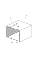
図4は、プローバが備えるアダプタユニットの外観を表す斜視図である。 FIG. 4 is a perspective view illustrating an appearance of an adapter unit included in the prober.
図4において、アダプタユニット25は、箱状のユニット本体40と、該ユニット本体40内に配されている複数のステージアーム41(基板収容手段)と、ユニット本体40内にステージアーム41の数と同じ数だけ配されているウエハ位置合わせ機構42と、底面48及び該底面48に対向する天井面(図示しない)に配置される複数の光学センサ43とを備える。
In FIG. 4, the
ユニット本体40では側面のうち3面が開口する。具体的には、ユニット本体40は、図3において、プローバ2のローダ室搬送アーム機構24に対向する面、プローバ2に対応して停止したRGV3のRGVアーム機構34に対向する面、及び該RGVアーム機構34に対向する面とは反対の面において開口部を有する。各開口部は各面のほぼ全域に亘って開口する。ローダ室搬送アーム機構24の搬送アーム241及びRGVアーム機構34の搬送アーム341は、各開口部を介してユニット本体40内に進入する。
In the unit
各ステージアーム41は底面48と平行をなし、搬送アーム241又は搬送アーム341によってユニット本体40内に搬入されたウエハの中心部を支持することにより、ウエハを載置する。これにより、アダプタユニット25はウエハを一時的に保管する。また、搬送アーム241又は搬送アーム341は、ステージアーム41によって支持されたウエハを搬出する。ウエハはステージアーム41による一時的な保管を介して搬送アーム241又は搬送アーム341によって搬出・搬入されるため、結果として、アダプタユニット25はウエハの受け渡しを行う。また、ステージアーム41は真空吸着機構(図示しない)を備え、載置したウエハを真空吸着する。なお、各ステージアーム41はウエハを1枚ずつ載置する。
Each
アダプタユニット25では、複数、例えば、8個のステージアーム41が底面48から天井面に向けて(上下方向に)互いに所定の間隔、例えば、20mmを保って配置される。なお、ステージアーム41の数は8個に限られず、8個から13個の間における任意の個数だけ配置可能である。
In the
ウエハ位置合わせ機構42は、平面視L字状のブロック部材であるロケーティングブロック421,422からなる。ロケーティングブロック421,422は、ローダ室搬送アーム機構24の搬送アーム241が搬送するウエハの中心の移動軌跡、すなわち、搬送アーム241によるウエハの搬送方向に関して互いに対称に配置される。搬送アーム241によって搬送されるウエハの外周部がロケーティングブロック421,422に当接することによってウエハの位置合わせが行われる。
The
また、アダプタユニット25は、底面48及び天井面においてそれぞれ複数、例えば、8個の光学センサ43を有する。これらの光学センサ43によってステージアーム41に載置されるウエハの位置ずれが検知される。各光学センサ43は外部の検知結果解析装置(図示しない)と接続されるための配線(図示しない)を有するため、該配線がユニット本体40内に突出して、搬送アーム241や搬送アーム341と干渉する虞がある。本実施の形態ではこれに対応して、搬送アーム241や搬送アーム341の進入経路の下に配置される光学センサ43の配線を覆う配線カバー49,50が底面48上に設けられる。これにより、各配線と搬送アーム241又は搬送アーム341との干渉を未然に防止することができる。
The
アダプタユニット25が備えるステージアームは、上述したウエハの中心部を支持するものに限られず、ウエハの外周部を支持するものであってもよい。この場合、ステージアームはウエハを挟んで対向するように配置された2つの支持部材からなるのが好ましい。
The stage arm provided in the
アダプタユニット25では、上下方向に隣接する2つのステージアーム41が20mmの間隔を保って配置される一方、RGVアーム機構34における上段の搬送アーム341の2つのピンセットが上下方向に20mmの間隔を保って配置されるので、上段の搬送アーム341は2枚のウエハを同時にアダプタユニット25へ搬入し、若しくはアダプタユニット25から搬出することができる。
In the
なお、基板搬送システムEにおける各プローバ2が備えるアダプタユニットは、上述したアダプタユニット25のように複数のウエハを収容可能なものに限られず、例えば、1つのウエハ載置台をのみを備えた1枚のウエハのみを収容可能なものであってもよい。プローバ2が備えるアダプタユニットの種類は、当該プローバ2における処理に要する時間に応じて決定される。具体的には、処理に要する時間が短い場合には複数のウエハを収容可能なアダプタユニットを備え、処理に要する時間が長い場合には1枚のウエハのみを収容可能なアダプタユニットを備えるのが好ましい。
Note that the adapter unit included in each
図5は、ストッカが備えるバッファの外観を表す斜視図である。 FIG. 5 is a perspective view illustrating an appearance of a buffer provided in the stocker.
図5において、バッファBは、箱状のユニット本体51と、該ユニット本体51内に配されている複数のウエハ載置部52とを備える。ユニット本体51では側面のうち1面が開口する。具体的には、ユニット本体51は、ストッカ10対応して停止したRGV3のRGVアーム機構34に対向する面において開口部53を有する。当該開口部は面のほぼ全域に亘って開口するが、オペレータによる搬出・搬入の際には蓋(図示しない)によって閉塞される。RGVアーム機構34の搬送アーム341は、開口部53を介してユニット本体51内に進入する。
In FIG. 5, the buffer B includes a box-shaped unit
各ウエハ載置部52は、開口部53を有する側面に隣接する側面のそれぞれから底面54と平行に突出する支持部材52a,52bからなり、搬送アーム341によってユニット本体51内に搬入されたウエハの外周部を支持することにより、ウエハを載置する。これにより、バッファBはウエハを一時的に保管する。また、搬送アーム341は、ウエハ載置部52によって支持されたウエハを搬出する。ウエハはウエハ載置部52による一時的な保管を介して搬送アーム341によって搬出・搬入されるため、結果として、バッファBはウエハの受け渡しを行う。なお、各ウエハ載置部52はウエハを1枚ずつ載置する。
Each
バッファBでは、複数のウエハ載置部52が底面53から天井面に向けて(上下方向に)互いに所定の間隔、例えば、20mmを保って配置される。ここで、上述したように、RGVアーム機構34における上段の搬送アーム341の2つのピンセットは上下方向に20mmの間隔を保って配置される。したがって、上段の搬送アーム341は2枚のウエハを同時にバッファBへ搬入し、若しくはバッファBから搬出することができる。
In the buffer B, a plurality of
上述した基板搬送システムEでは、RGVアーム機構34における上段の搬送アーム341は、2枚のウエハを同時にアダプタユニット25へ搬入し、若しくはアダプタユニット25から搬出することができ、さらに、2枚のウエハを同時にバッファBへ搬入し、若しくはバッファBから搬出することができるので、ウエハの搬送効率を向上することができる。
In the substrate transfer system E described above, the
次に、本実施の形態に係る基板搬送方法について説明する。 Next, a substrate transfer method according to the present embodiment will be described.
従来の基板搬送システムでは、RGVがウエハを搬送する際、ストッカ又はプローバから受け取ったウエハを一旦RGVのバッファ内に収容して搬送するため、ストッカ又はプローバとのウエハの受け渡しにおいて、ウエハのバッファへの収容及びバッファからの取り出しが発生し、ウエハの搬送効率の向上を妨げていた。 In the conventional substrate transport system, when the RGV transports a wafer, the wafer received from the stocker or prober is once accommodated in the buffer of the RGV and transported. Therefore, when the wafer is transferred to and from the stocker or prober, it is transferred to the wafer buffer. And the removal from the buffer occurred, preventing improvement in wafer transfer efficiency.
本実施の形態に係る基板搬送方法は、これに対応して、RGV3がウエハをバッファBFに収容することなく搬送する。
Correspondingly, in the substrate transfer method according to the present embodiment, the
図6は、本実施の形態に係る基板搬送方法の一例を示す工程図である。 FIG. 6 is a process diagram showing an example of a substrate carrying method according to the present embodiment.
図6において、ストッカ10のバッファBに対向するように停止したRGV3は、搬送アーム341を延伸させることによって当該搬送アーム341をバッファBに進入させ、ウエハWをバッファBから搬出する(図6(A))。
In FIG. 6, the
次いで、ウエハWを搬出した搬送アーム341は、ウエハWを載置したまま収縮するが、当該ウエハWをバッファBFに収容しない。換言すれば、ウエハWを搬出した搬送アーム341はウエハWを載置したまま動作を中断する。そして、RGV3は、搬送アーム341にウエハWを載置させたままレール12に沿って所定のプローバ2まで移動する(図6(B))。
Next, the
次いで、所定のプローバ2まで移動してアダプタユニット25に対向するように停止したRGV3は、ウエハWを載置した搬送アーム341を延伸させることによって当該搬送アーム341をアダプタユニット25に進入させ、ウエハWをアダプタユニット25へ搬入する(図6(C))。
Next, the
上述した図6の基板搬送方法によれば、ウエハWを搬出した搬送アーム341がウエハWを載置したまま動作を中断し、RGV3が搬送アーム341にウエハWを載置させたまま移動するので、RGV3においてウエハWをバッファBFに収容する必要及びウエハWをバッファBFから取り出す必要を無くすことができ、もって、ウエハWの搬送効率を向上することができる。
According to the substrate transfer method of FIG. 6 described above, the
RGV3が移動する際にウエハを載置する搬送アーム341は、RGVアーム機構34における上段及び下段の搬送アーム341のいずれでもよいが、上段の搬送アーム341であれば、当該上段の搬送アーム341は上述したように、2枚のウエハを同時にバッファBから搬出することができる、すなわち、2枚のウエハを載置することができるので、RGV3が搬送アーム341に2枚のウエハWを載置させたまま移動することができ、もって、よりウエハWの搬送効率を向上することができる。
The
なお、上段の搬送アーム341及び下段の搬送アーム341のいずれもがウエハWをバッファBから搬出し、RGV3が上段の搬送アーム341及び下段の搬送アーム341のそれぞれにウエハWを載置させたまま移動してもよく、これにより、さらにウエハWの搬送効率を向上することができる。
Note that both the
また、上述した図6の基板搬送方法では、RGV3が搬送アーム341にウエハWを載置させたままストッカ10からプローバ2へ移動したが、RGV3は搬送アーム341にウエハWを載置させたままプローバ2からストッカ10、若しくは一のプローバ2から他のプローバ2へ移動してもよく、これにより、プローバ2からストッカ10、若しくは一のプローバ2から他のプローバ2へのウエハWの搬送効率を向上することができる。
In the substrate transfer method of FIG. 6 described above, the
さらに、上述した図6の基板搬送方法では、自在に伸縮する搬送アーム341がバッファBからウエハWを搬出し、該ウエハWをアダプタユニット25に搬入するので、ウエハWの搬出・搬入(受け渡し)を円滑に行うことができ、もって、ウエハWの搬送効率を向上することができる。
Furthermore, in the substrate transfer method of FIG. 6 described above, the
上述した図6の基板搬送方法では、搬送アーム341がウエハWをバッファBFに収容しないが、搬送アーム341がバッファBから複数枚のウエハWを搬出する場合、搬送アーム341は搬出した複数のウエハWのうち何枚かをバッファBFに格納し、最後に搬出したウエハWのみをバッファBFに収容することなくそのまま載置してもよい。
In the substrate transfer method of FIG. 6 described above, the
ところで、従来の基板搬送システムにおけるRGVの搬送アームは、予め設定されたウエハの搬送先である目標位置に向けてウエハを搬送する。ここで、RGVの搬送アームは目標位置以外において動作、例えば、伸縮を中断することがない。 By the way, the RGV transfer arm in the conventional substrate transfer system transfers the wafer toward a preset target position which is a transfer destination of the wafer. Here, the transfer arm of the RGV does not interrupt the operation other than the target position, for example, expansion and contraction.
一方、本実施の形態に係る基板搬送方法では、ウエハWを搬出した搬送アーム341がウエハWを載置したまま動作を中断する必要がある。そこで、基板搬送システムEでは、搬送アーム341がウエハWを載置したまま動作を中断する搬送アーム動作中断位置が設定されている。搬送アーム動作中断位置は、ウエハWを搬出した搬送アーム341が収縮した位置であって、搬送アーム341が載置するウエハWがRGV3のほぼ中央に位置するような位置である(図6(B)参照。)。したがって、基板搬送システムEでは、ウエハWの搬送先である目標位置として、ストッカ10に該当する「ST」、RGV3のバッファBFに該当する「BF」、及びプローバ2に該当する「EQ」が設定され、さらに、搬送アーム動作中断位置として、搬送アーム341が収縮した位置に該当する「PBF」が設定されている。
On the other hand, in the substrate transfer method according to the present embodiment, it is necessary to interrupt the operation of the
上述した基板搬送システムEによれば、「PBF」が設定されているので、RGV3が移動する間に搬送アーム341によってウエハWをPBFに位置させることにより、RGV3が搬送アーム341にウエハWを載置させたまま移動することができ、これにより、RGV3においてウエハWをバッファBFに収容する必要及びウエハWをバッファBFから取り出す必要を無くすことができ、もって、ウエハWの搬送効率を向上することができる。
According to the substrate transfer system E described above, since “PBF” is set, the wafer W is placed on the
また、「PBF」は、RGVアーム機構34における上段の搬送アーム341及び下段の搬送アーム341の両方、又はいずれか一方のみについて設定されてもよい。これにより、ウエハの搬送形態の選択肢を増やすことができ、もって、よりウエハWの搬送効率を向上することができる。
“PBF” may be set for both or only one of the
従来、基板搬送システムでは、搬送アームによるウエハの搬送手順(以下、「搬送シーケンス」という。)がホストコンピュータによって設定されている。ホストコンピュータは、オペレータからの入力等に応じて複数の後述する搬送コマンドを組み合わせることによって搬送シーケンスを設定する。搬送コマンドは、搬送アームによるウエハの搬送経路を規定するコマンドであり、基板搬送システムではウエハの搬送先である目標位置の組み合わせ可能な数に対応して複数のコマンドが予め準備されている。具体的には、各コマンドはホストコンピュータが備えるHDD(図示しない)等に格納されている。 Conventionally, in a substrate transfer system, a wafer transfer procedure (hereinafter referred to as “transfer sequence”) by a transfer arm is set by a host computer. The host computer sets a conveyance sequence by combining a plurality of later-described conveyance commands in accordance with an input from the operator. The transfer command is a command for defining the transfer route of the wafer by the transfer arm. In the substrate transfer system, a plurality of commands are prepared in advance corresponding to the number of target positions that can be transferred to the wafer. Specifically, each command is stored in an HDD (not shown) provided in the host computer.
各搬送コマンドでは、ウエハの搬送元及び搬送先が規定されている。設定された搬送シーケンスはRGVコントローラに送信され、RGVコントローラは無線通信によって搬送シーケンスをRGVに通知し、RGVは、通知された搬送シーケンスに従ってストッカ及び複数のプローバの間を移動してウエハを搬送する。 In each transfer command, the transfer source and transfer destination of the wafer are defined. The set transfer sequence is transmitted to the RGV controller, and the RGV controller notifies the transfer sequence to the RGV by wireless communication. The RGV moves between the stocker and the plurality of probers according to the notified transfer sequence and transfers the wafer. .
ここで、上述したように、本実施の形態に係る基板搬送システムとしての基板搬送システムEでは、目標位置としての「ST」、「BF」、及び「EQ」の他に搬送アーム341が収縮した位置に該当する「PBF」が設定されるため、ウエハの搬送元又は搬送先として「PBF」が設定された搬送コマンドが予め準備されている。すなわち、予め準備されている複数の搬送コマンドのうち、幾つかの搬送コマンドが規定する搬送経路には、搬送先、搬送元若しくは経由箇所として「PBF」が設定されている。
Here, as described above, in the substrate transport system E as the substrate transport system according to the present embodiment, the
以下、基板搬送システムEにおける搬送コマンドの具体例について説明する。 Hereinafter, a specific example of the transfer command in the substrate transfer system E will be described.
基板搬送システムEにおける搬送コマンドの種類としては、一の搬送アーム341が単独で他の搬送アーム341と連携することなくウエハを搬送する単独動作モードと、上段及び下段の搬送アーム341が連続して同じ搬送経路でウエハを搬送する連続動作モードと、一の搬送アーム341がウエハをアダプタユニット25又はバッファBから搬出し、次いで、他の搬送アーム341が他のウエハをアダプタユニット25又はバッファBへ搬入する入れ換え動作モードとがある。
As the types of transfer commands in the substrate transfer system E, one
下記表1は、基板搬送システムEにおいて予め準備されている単独動作モードの搬送コマンドのリストであり、図7は、単独動作モードの各搬送コマンドが規定する搬送経路を示す図である。 Table 1 below is a list of transfer commands in the single operation mode prepared in advance in the substrate transfer system E, and FIG. 7 is a diagram showing transfer paths defined by the transfer commands in the single operation mode.

表1において、「CASE」は各搬送コマンドの名称であり、「FROM」は搬送元を示し、「TO」は搬送先を示す。また、網掛けされている搬送元及び搬送先は搬送コマンドにおける経由箇所を示し、例えば、搬送コマンドEは「ST」から「EQ」までの搬送経路を規定するが、「ST」から「EQ」までの間に「PBF」を経由する。具体的には、搬送コマンドEではウエハをまず「ST」から「PBF」まで搬送し、さらに「PBF」から「EQ」まで搬送する。 In Table 1, “CASE” is the name of each transfer command, “FROM” indicates the transfer source, and “TO” indicates the transfer destination. Further, the transfer source and transfer destination that are shaded indicate a transit point in the transfer command. For example, the transfer command E defines a transfer path from “ST” to “EQ”, but “ST” to “EQ”. Until “PBF”. Specifically, in the transfer command E, the wafer is first transferred from “ST” to “PBF”, and further transferred from “PBF” to “EQ”.
図7では、各搬送コマンドが規定する搬送経路が矢印で示されるが、「( )」付きで示される搬送コマンドは、該搬送コマンドが附される矢印とは反対向きの搬送経路を規定する。 In FIG. 7, the conveyance path defined by each conveyance command is indicated by an arrow, but the conveyance command indicated by “()” defines a conveyance path opposite to the arrow to which the conveyance command is attached.
基板搬送システムEでは従来の基板搬送システムに対して「PBF」が追加して設定されているので、単独動作モードにおいて搬送コマンド「A−1」,「A−2」,「B−1」,「B−2」,「C−1」,「C−2」,「D−1」,「D−2」,「E」,「F」,「G」,「H」,「I」が追加されている。 In the substrate transfer system E, since “PBF” is additionally set with respect to the conventional substrate transfer system, the transfer commands “A-1”, “A-2”, “B-1”, “B-2”, “C-1”, “C-2”, “D-1”, “D-2”, “E”, “F”, “G”, “H”, “I” Have been added.
下記表2は、基板搬送システムEにおいて予め準備されている連続動作モードの搬送コマンドのリストであり、図8は、連続動作モードの各搬送コマンドが規定する搬送経路を示す図である。 Table 2 below is a list of transfer commands in the continuous operation mode prepared in advance in the substrate transfer system E, and FIG. 8 is a diagram showing transfer paths defined by the transfer commands in the continuous operation mode.
表2における「CASE」,「FROM」,「TO」は表1のものと同じであり、網掛けの意味も表1と同じである。 “CASE”, “FROM”, and “TO” in Table 2 are the same as those in Table 1, and the meaning of shading is the same as in Table 1.
図8では、矢印で示される搬送経路のうち、実線で示される矢印は上段の搬送アーム341の搬送経路であり、破線で示される矢印は下段の搬送アーム341の搬送経路である。また、「( )」付きで示される搬送コマンドは、該搬送コマンドが附される矢印とは反対向きの搬送経路を規定する。
In FIG. 8, among the transfer paths indicated by arrows, the arrow indicated by a solid line is the transfer path of the
連続動作モードの搬送コマンド「A」,「B」,「C」,「D」,「E」,「F」,「G」,「H」,「I」では、経由箇所、搬送先若しくは搬送元に「PBF」が設定されているので、これらの搬送コマンドは従来の基板搬送システムでは準備されていない搬送コマンドである。 In the transfer commands “A”, “B”, “C”, “D”, “E”, “F”, “G”, “H”, “I” in the continuous operation mode, the via point, the transfer destination or the transfer Since “PBF” is originally set, these transfer commands are transfer commands that are not prepared in the conventional substrate transfer system.
下記表3は、基板搬送システムEにおいて予め準備されている入れ換え動作モードの搬送コマンドのリストであり、図9は、入れ換え動作モードの各搬送コマンドが規定する搬送経路を示す図である。 Table 3 below is a list of transfer commands in the replacement operation mode prepared in advance in the substrate transfer system E, and FIG. 9 is a diagram showing transfer paths defined by the transfer commands in the replacement operation mode.
表3における「CASE」,「FROM」,「TO」は表1のものと同じである。 “CASE”, “FROM”, and “TO” in Table 3 are the same as those in Table 1.
図9では、矢印で示される搬送経路のうち、実線で示される矢印は上段の搬送アーム341の搬送経路であり、破線で示される矢印は下段の搬送アーム341の搬送経路である。また、「( )」付きで示される搬送コマンドは、該搬送コマンドが附される矢印とは反対向きの搬送経路を規定する。
In FIG. 9, among the transfer paths indicated by arrows, the arrow indicated by a solid line is the transfer path of the
入れ換え動作モードの搬送コマンドのうち、搬送コマンド「C」,「D」,「G」,「H」,「I」,「J」,「K」,「L」では、経由箇所、搬送先若しくは搬送元に「PBF」が設定されているので、これらの搬送コマンドは従来の基板搬送システムでは準備されていない搬送コマンドである。 Among the transfer commands in the replacement operation mode, the transfer commands “C”, “D”, “G”, “H”, “I”, “J”, “K”, “L” have a transit point, a transfer destination or Since “PBF” is set as the transfer source, these transfer commands are transfer commands not prepared in the conventional substrate transfer system.
上述した基板搬送システムEによれば、ホストコンピュータ1は「PBF」が設定されている搬送経路を規定する搬送コマンドを含む複数の搬送コマンドを組み合わせてウエハの搬送シーケンスを設定するので、設定された搬送シーケンスにおいて、RGV3が「PBF」において搬送アーム341にウエハを載置させたまま移動することができ、これにより、RGV3においてウエハをバッファBFに収容する必要及びウエハをバッファBFから取り出す必要を無くすことができ、もって、ウエハの搬送効率を向上することができる。
According to the substrate transfer system E described above, the
また、上述した基板搬送システムEによれば、搬送経路における経由箇所、搬送先若しくは搬送元に「PBF」が設定されているので、搬送コマンドの種類を従来の基板搬送システムと比較して大幅に増やすことができ、搬送シーケンスに関する設定の自由度を増すことができ、例えば、各搬送コマンドを最適に組み合わせて搬送シーケンスを設定することにより、ウエハの搬送時間を大幅に短縮することができ、もって、よりウエハの搬送効率を向上することができる。 Further, according to the above-described substrate transfer system E, since “PBF” is set as the transit point, transfer destination or transfer source in the transfer route, the type of transfer command is greatly compared with the conventional substrate transfer system. It is possible to increase the degree of freedom for setting the transfer sequence.For example, by setting the transfer sequence by optimally combining the transfer commands, the wafer transfer time can be greatly shortened. Thus, the wafer transfer efficiency can be further improved.
上述した基板搬送システムEでは、ホストコンピュータ1が連続動作モードの搬送コマンドや入れ換え動作モードの搬送コマンドを用いて搬送シーケンスを設定する場合には、上段の搬送アーム341及び下段の搬送アーム341に共通の搬送シーケンスのみを設定するが、ホストコンピュータ1が、連続動作モードの搬送コマンドや入れ換え動作モードの搬送コマンドを用いずに上段の搬送アーム341及び下段の搬送アーム341のそれぞれに対して異なる搬送シーケンスを設定してもよい。このとき、上段の搬送アーム341及び下段の搬送アーム341の搬送経路は異なる。これにより、搬送シーケンスに関する設定の自由度をさらに増すことができる。
In the substrate transport system E described above, when the
基板搬送システムEにおける入れ換え動作モードの各搬送コマンドでは、一の搬送アーム341がウエハをアダプタユニット25又はバッファBから搬出し、次いで、他の搬送アーム341が他のウエハをアダプタユニット25又はバッファBへ搬入するので、ウエハの入れ換えを迅速に行うことができる。したがって、入れ換え動作モードの各搬送コマンドを用いて搬送シーケンスを設定すれば、さらにウエハの搬送効率を向上することができる。
In each transfer command in the exchange operation mode in the substrate transfer system E, one
また、基板搬送システムEにおける連続動作モードの各搬送コマンドでは、上段及び下段の搬送アーム341が連続して同じ搬送経路でウエハを搬送するので、複数のウエハが連続的に搬送される。したがって、連続動作モードの各搬送コマンドを用いて搬送シーケンスを設定すれば、よりウエハの搬送効率を向上することができる。
Further, in each transfer command in the continuous operation mode in the substrate transfer system E, the upper and
次いで、図1の基板搬送システムにおいて実行されるウエハ搬送処理について説明する。 Next, a wafer transfer process executed in the substrate transfer system of FIG. 1 will be described.
従来の基板搬送システムでは、搬送シーケンスに従ってプローバまで移動したRGVが当該プローバと光結合PIO通信を行った後に、プローバはホストコンピュータにRGVが到着した旨及びプローバの状態、例えば、ウエハを受け入れ可能であるか否かを連絡し、該連絡を受信したホストコンピュータは、RGVが搬送するウエハの諸元、例えば、ID番号、処理履歴、処理内容(レシピデータ)、処理時間、処理優先度、ウエハを載置すべきステージアームの位置(スロット番号)をプローバに連絡する。そして、連絡を受信したプローバは光結合PIO通信によってウエハの搬入を許可する旨をRGVに連絡し、該連絡を受信したRGVはウエハをアダプタユニットへ搬入する。 In the conventional substrate transfer system, after the RGV that has moved to the prober according to the transfer sequence performs optical coupling PIO communication with the prober, the prober can accept that the RGV has arrived at the host computer and the status of the prober, for example, a wafer. The host computer that has received the notification determines whether or not the specifications of the wafer carried by the RGV, such as ID number, processing history, processing contents (recipe data), processing time, processing priority, and wafer, Report the position (slot number) of the stage arm to be placed to the prober. Then, the prober that has received the notification notifies the RGV that the wafer loading is permitted by optical coupling PIO communication, and the RGV that has received the communication loads the wafer into the adapter unit.
しかしながら、プローバはRGVがプローバまで移動した後に当該プローバの状態をホストコンピュータに連絡するので、プローバがウエハを受け入れ不可能な状態にある場合、RGVによるストッカからプローバまでの移動工程が無駄になることがあった。 However, since the prober informs the host computer of the status of the prober after the RGV has moved to the prober, the process of moving from the stocker to the prober by the RGV is wasted if the prober is in an unacceptable state. was there.
また、アダプタユニットにおけるステージアームが真空吸着可能になるまでには、真空吸着機構を起動してから所定の時間を要するため、RGVがプローバまで移動した後に、ホストコンピュータからスロット番号の連絡を受信して、受信したスロット番号に対応するステージアームの真空吸着機構を起動したのでは、ウエハのアダプタユニットへの搬入に関して待ち時間が発生することがあった。 Also, since it takes a predetermined time after the vacuum suction mechanism is activated before the stage arm in the adapter unit can be vacuum-sucked, the RGV receives the slot number notification from the host computer after moving to the prober. Thus, when the vacuum suction mechanism of the stage arm corresponding to the received slot number is activated, a waiting time may occur with respect to the wafer loading into the adapter unit.
以下に詳述するウエハ搬送処理では、これに対応して、RGVがプローバに移動する前にホストコンピュータがプローバへ搬送するウエハの諸元を連絡し、また、プローバが当該プローバの状態をホストコンピュータに連絡する。 Correspondingly, in the wafer transfer process described in detail below, before the RGV moves to the prober, the host computer informs the specifications of the wafer to be transferred to the prober, and the prober indicates the status of the prober. Contact
図10は、図1の基板搬送システムにおいて実行されるウエハ搬送処理のフローチャートである。 FIG. 10 is a flowchart of wafer transfer processing executed in the substrate transfer system of FIG.
図10において、まず、オペレータによって所定の検査処理の指示が入力されると、ホストコンピュータ1は当該所定の検査処理においてウエハの電気的特性検査を行う各プローバ2にこれから搬送するウエハの諸元、例えば、ID番号、処理履歴、処理内容(レシピデータ)、処理時間、処理優先度、スロット番号を通知するとともに、各プローバ2の状態を問い合わせる(ステップS101)(状態問い合わせステップ)。
In FIG. 10, first, when an instruction for a predetermined inspection process is input by the operator, the
次いで、各プローバ2は、受信したウエハの諸元に基づいてウエハの受け入れ準備、例えば、受信したスロット番号に対応するステージアーム41の真空吸着機構の起動を行うと共に、当該プローバ2の状態、例えば、ウエハを受け入れ可能であるか否か、受信したスロット番号に対応するステージアーム41がウエハを載置しているか否か(空きスロットか否か)、並びに、ウエハを載置していないステージアーム41の数(空きスロットの数)をホストコンピュータ1に連絡する(ステップS102)(状態連絡ステップ)。
Next, each
次いで、各プローバ2の状態の連絡を受信したホストコンピュータ1は、各プローバ2の状態に応じて搬送シーケンスを設定する(ステップS103)(搬送シーケンス設定ステップ)。例えば、ウエハを受け入れ不可能な状態にあるプローバ2があれば、当該プローバ2を通過するように搬送シーケンスを設定する。また、ホストコンピュータ1は、受信した空きスロットの数に応じてアダプタユニット25へウエハを搬入する搬送アーム341を選択する。より具体的には、空きスロットの数が複数であり、少なくとも2つの空きスロットが隣接する場合には、2枚のウエハを同時に搬入可能な上段の搬送アーム341によってウエハをアダプタユニット25に搬入するように搬送シーケンスが設定され、空きスロットの数が1である場合や、互いに隣接する空きスロットが存在していない場合には、1枚のウエハをのみを搬入可能な下段の搬送アーム341によってウエハをアダプタユニット25に搬入するように搬送シーケンスが設定される。
Next, the
次いで、ホストコンピュータ1は設定した搬送シーケンスをRGVコントローラ4に送信し、RGVコントローラ4は無線通信によって搬送シーケンスをRGV3に通知する(ステップS104)(搬送シーケンス通知ステップ)。
Next, the
次いで、RGV3は、入力された搬送シーケンスに従って、まず、ストッカ10まで移動し、当該ストッカ10から所定枚数のウエハを搬出する(ステップS105)。そして、RGV3は所定枚数のうち何枚かをバッファBFに格納し、残りのウエハを搬送アーム341に載置させたまま、所定のプローバ2へ移動する(ステップS106)(移動ステップ)。
Next, the
次いで、RGV3は所定のプローバ2まで移動すると、当該プローバと光結合PIO通信を行う(ステップS107)。このとき、RGV3はPIO通信によって当該RGV3が到着した旨をプローバ2に連絡すると共に、プローバ2が備えるアダプタユニットの種類を問い合わせ(ステップS108)(基板受け渡し部種類問い合わせステップ)、問い合わせを受信したプローバ2は当該プローバ2が備えるアダプタユニットの種類をRGV3に連絡する(ステップS109)(基板受け渡し部種類連絡ステップ)。
Next, when the
次いで、RGV3は受信したアダプタユニットの種類が、搬送シーケンスにおいて規定されている搬送アーム341が搬入可能なウエハの枚数と整合しているか否かを判別し(ステップS110)、アダプタユニットの種類が搬入可能なウエハの枚数と整合している場合、例えば、アダプタユニットが複数のウエハを受け入れ可能なアダプタユニット25であり、搬送シーケンスにおいて規定されている搬送アーム341が上段又は下段の搬送アーム341である場合には、ウエハをアダプタユニットへ搬入し(ステップS111)、アダプタユニットの種類が搬入可能なウエハの枚数と整合していない場合、例えば、アダプタユニットが1枚のウエハのみを受け入れ可能なアダプタユニットであり、搬送シーケンスにおいて規定されている搬送アーム341が上段の搬送アーム341である場合には、ステップS111をスキップしてウエハをアダプタユニットへ搬入することなくステップS112へ進む。なお、RGV3はステップS108においてプローバ2が備えるアダプタユニットの種類を問い合わせ後、所定時間の間にプローバ2から連絡がない場合にも直ちにステップS112へ進む。
Next, the
次いで、RGV3は搬送シーケンスにおいて規定されたウエハの搬送先としてのプローバ2が残っているか否かを判別し(ステップS112)、搬送先としてのプローバ2が残っている場合には、ステップS106へ戻り、搬送先としてのプローバ2が残っていない場合には、本処理を終了する。
Next, the
図10のウエハ搬送処理によれば、ホストコンピュータ1が搬送されるウエハの諸元をプローバ2に通知すると共に、プローバ2の状態を問い合わせ(ステップS101)、状態を問い合わされたプローバ2が当該プローバ2の状態をホストコンピュータ1に連絡し(ステップS102)、ホストコンピュータ1が連絡された状態に基づいて搬送シーケンスを設定し(ステップS103)、ホストコンピュータ1が設定された搬送シーケンスをRGVコントローラ4を介してRGV3に通知する(ステップS104)ので、プローバ2は予め搬送されてくるウエハの諸元を知ることができ、もって、ウエハが搬送された後に該ウエハの諸元をホストコンピュータ1に問い合わす必要を無くすことができ、また、プローバ2がウエハを受け入れ不可能な状態にある場合にRGV3は当該プローバ2を通過することができる。これにより、ウエハの搬送効率を向上することができる。さらに、RGV3が移動を開始した後、ホストコンピュータ1とプローバ2との間において通信障害が発生しても、プローバ2は搬送されてくるウエハの諸元を既に知っているため、以降の検査処理において支障を来すことがない。
According to the wafer transfer process of FIG. 10, the
また、図10のウエハ搬送処理では、RGV3が搬送アーム341にウエハを載置させたまま移動する(ステップS106)ので、RGV3においてウエハをバッファBFに収容する必要及びウエハをバッファBFから取り出す必要を無くすことができ、もって、よりウエハの搬送効率を向上することができる。
In the wafer transfer process of FIG. 10, since the
さらに、図10のウエハ搬送処理では、RGV3によるウエハの搬入前に、プローバ2がアダプタユニットの種類をRGV3に連絡する(ステップS109)ので、RGV3が同時にプローバ2に搬入可能なウエハの枚数と、プローバ2が同時に受け入れ可能なウエハの枚数との整合を確認することができ、もって、ウエハの受け渡しを確実に行うことができる。これにより、RGV3が移動している途中にオペレータがプローバ2のアダプタユニットを取り替えてもアダプタユニットへのウエハの搬入に支障を来すことがない。
Further, in the wafer transfer process of FIG. 10, the
また、図10のウエハ搬送処理によれば、搬送シーケンスの設定の際、空きスロットの数に応じて、アダプタユニットにウエハを受け渡す搬送アーム341が選択されるので、空きスロットの数と、搬送アーム341が搬入可能なウエハの枚数とを整合させることができ、もって、ウエハの搬送効率を向上することができる。
In addition, according to the wafer transfer processing of FIG. 10, when setting the transfer sequence, the
さらに、図10のウエハ搬送処理では、空きスロットの数が1である場合、1枚のウエハをのみを搬入可能な下段の搬送アーム341が選択されるので、搬送アーム341がアダプタユニットにウエハを受け渡すことができない事態の発生を防止することができる。
Furthermore, in the wafer transfer process of FIG. 10, when the number of empty slots is 1, the
上述した基板搬送システムEは、基板処理装置としてプローバを備えたが、基板処理装置の種類はこれに限られず、ウエハに所定の処理を施す装置、例えば、プラズマ処理装置(エッチング処理装置、CVD処理装置)であってもよい。また、基板搬送システムEが備える基板処理装置は枚葉でウエハを処理する装置に限られず、複数枚のウエハをバッチ処理する装置であってもよい。さらに、基板搬送システムEが備える基板処理装置の数も複数に限られず、1つであってもよい。 The substrate transfer system E described above includes a prober as a substrate processing apparatus. However, the type of the substrate processing apparatus is not limited to this, and an apparatus that performs predetermined processing on a wafer, for example, a plasma processing apparatus (etching processing apparatus, CVD processing). Device). Further, the substrate processing apparatus included in the substrate transfer system E is not limited to an apparatus that processes wafers on a single sheet, and may be an apparatus that batch processes a plurality of wafers. Further, the number of substrate processing apparatuses provided in the substrate transfer system E is not limited to a plurality, and may be one.
また、基板搬送システムEにおいて搬送される基板は半導体デバイス用のウエハに限られず、LCD(Liquid Crystal Display)やFPD(Flat Panel Display)等に用いる各種基板や、フォトマスク、CD基板、プリント基板等であってもよい。 In addition, the substrate transported in the substrate transport system E is not limited to a wafer for a semiconductor device. Various substrates used for LCD (Liquid Crystal Display), FPD (Flat Panel Display), etc., photomasks, CD substrates, printed substrates, etc. It may be.
本発明の目的は、上述した本実施の形態の機能を実現するソフトウェアのプログラムコードを記録した記憶媒体を、コンピュータ、例えば、ホストコンピュータ1やRGVコントローラ4に供給し、コンピュータのCPUが記憶媒体に収容されたプログラムコードを読み出して実行することによっても達成される。
An object of the present invention is to supply a computer, for example, the
この場合、記憶媒体から読み出されたプログラムコード自体が上述した本実施の形態の機能を実現することになり、プログラムコード及びそのプログラムコードを記憶した記憶媒体は本発明を構成することになる。 In this case, the program code itself read from the storage medium realizes the functions of the above-described embodiment, and the program code and the storage medium storing the program code constitute the present invention.
また、プログラムコードを供給するための記憶媒体としては、例えば、RAM、NV−RAM、フロッピー(登録商標)ディスク、ハードディスク、光ディスク、光磁気ディスク、CD−ROM、CD−R、CD−RW、DVD(DVD−ROM、DVD−RAM、DVD−RW、DVD+RW)、磁気テープ、不揮発性のメモリカード、他のROM等の上記プログラムコードを記憶できるものであればよい。或いは、上記プログラムコードは、インターネット、商用ネットワーク、若しくはローカルエリアネットワーク等に接続される不図示の他のコンピュータやデータベース等からダウンロードすることによりコンピュータに供給されてもよい。 Examples of the storage medium for supplying the program code include RAM, NV-RAM, floppy (registered trademark) disk, hard disk, optical disk, magneto-optical disk, CD-ROM, CD-R, CD-RW, and DVD. (DVD-ROM, DVD-RAM, DVD-RW, DVD + RW), magnetic tape, non-volatile memory card, other ROM, etc. may be used as long as they can store the program code. Alternatively, the program code may be supplied to the computer by downloading from another computer or database (not shown) connected to the Internet, a commercial network, a local area network, or the like.
また、コンピュータが読み出したプログラムコードを実行することにより、上記本実施の形態の機能が実現されるだけでなく、そのプログラムコードの指示に基づき、CPU上で稼動しているOS(オペレーティングシステム)等が実際の処理の一部又は全部を行い、その処理によって上述した本実施の形態の機能が実現される場合も含まれる。 Further, by executing the program code read by the computer, not only the functions of the present embodiment are realized, but also an OS (operating system) running on the CPU based on the instruction of the program code, etc. Includes a case where part or all of the actual processing is performed and the above-described functions of the present embodiment are realized by the processing.
更に、記憶媒体から読み出されたプログラムコードが、コンピュータに挿入された機能拡張ボードやコンピュータに接続された機能拡張ユニットに備わるメモリに書き込まれた後、そのプログラムコードの指示に基づき、その機能拡張ボードや機能拡張ユニットに備わるCPU等が実際の処理の一部又は全部を行い、その処理によって上述した本実施の形態の機能が実現される場合も含まれる。 Further, after the program code read from the storage medium is written into a memory provided in a function expansion board inserted into the computer or a function expansion unit connected to the computer, the function expansion is performed based on the instruction of the program code. This includes a case where the CPU or the like provided in the board or the function expansion unit performs part or all of the actual processing, and the above-described functions of the present embodiment are realized by the processing.
上記プログラムコードの形態は、オブジェクトコード、インタプリタにより実行されるプログラムコード、OSに供給されるスクリプトデータ等の形態から成ってもよい。 The form of the program code may include an object code, a program code executed by an interpreter, script data supplied to the OS, and the like.
B,BF バッファ
E 基板搬送システム
W ウエハ
2 プローバ
10 ストッカ
12 レール
21 ローダ室
22 プローバ室
24 ローダ室搬送アーム機構
25 アダプタユニット
3 RGV
34 RGVアーム機構
341 アーム
4 RGVコントローラ
40 ユニット本体
41 ステージアーム
B, BF Buffer E Substrate transfer
34
Claims (10)
前記基板処理装置は複数の前記基板を受け渡す基板受け渡し部を有し、前記基板受け渡し部は前記基板を収容する複数の基板収容手段を有し、前記基板収容手段はそれぞれ1枚の前記基板を収容し、
前記基板搬送装置は複数の前記基板搬送手段を備え、前記複数の基板搬送手段の少なくとも1つは複数の前記基板を保持すると共に、他の前記基板搬送手段のうち少なくとも1つが1枚の前記基板を保持し、
前記基板受け渡し部における前記基板を収容していない前記基板収容手段の数に応じて、前記基板受け渡し部に前記基板を受け渡す基板搬送手段が前記複数の基板搬送手段から選択され、前記基板搬送装置全体が前記基板搬送手段に前記基板を保持させたまま移動可能であることを特徴とする基板搬送システム。 A substrate storage device storing substrate, at least one substrate processing apparatus performs a predetermined process on the substrate, and a substrate transfer device for transferring the substrate by moving between the substrate storing apparatus and the substrate processing apparatus , wherein the substrate transfer apparatus to hold the substrate, and unloading the substrate from the substrate storage device or the substrate processing apparatus, and, for carrying the substrate into the substrate storage device or the substrate processing apparatus a substrate transport system comprising at least one substrate transfer means,
The substrate processing apparatus includes a substrate transfer unit that transfers a plurality of the substrates, the substrate transfer unit includes a plurality of substrate storage units that store the substrates, and each of the substrate storage units includes one substrate. Contain,
The substrate transport apparatus includes a plurality of the substrate transport means, and at least one of the plurality of substrate transport means holds the plurality of substrates, and at least one of the other substrate transport means includes one substrate. Hold
In accordance with the number of the substrate accommodation units that do not accommodate the substrate in the substrate delivery unit, a substrate conveyance unit that delivers the substrate to the substrate delivery unit is selected from the plurality of substrate conveyance units , and the substrate conveyance apparatus substrate transfer system, wherein the whole is movable while keeping holding the substrate on the substrate transfer means.
前記基板搬送装置は前記複数の基板処理装置の間を移動することを特徴とする請求項1又は2記載の基板搬送システム。 The substrate transport system includes a plurality of the substrate processing apparatuses,
The substrate transfer system according to claim 1 or 2, wherein the substrate transfer apparatus, characterized in that moves between the plurality of substrate processing apparatus.
前記制御装置は、前記複数の搬送命令のうち少なくとも1つが規定する搬送経路に、前記基板搬送手段が前記基板を保持したまま動作を中断する動作中断位置を設定することを特徴とする請求項1記載の基板搬送システム。 A control device that sets a transport sequence of the substrate by combining a plurality of transport commands defining a transport route of the substrate by the substrate transport means;
Claim wherein the controller, at least one of the plurality of transport instructions but the conveyance path defining, for the substrate transfer means, characterized in that you set the suspend operation interruption position the operation while holding the substrate 2. The substrate transfer system according to 1.
前記制御装置は前記複数の基板搬送手段による前記基板の搬送を連続的に行うか又は搬送経路が互いに異なる前記搬送シーケンスを設定することを特徴とする請求項4記載の基板搬送システム。 The substrate transport apparatus has a plurality of the substrate transport means,
5. The substrate transfer system according to claim 4, wherein the control device continuously transfers the substrate by the plurality of substrate transfer means, or sets the transfer sequence having different transfer paths.
前記基板処理装置は、複数の前記基板を受け渡す基板受け渡し部を有し、前記基板受け渡し部は前記基板を収容する複数の基板収容手段を有し、前記基板収容手段はそれぞれ1枚の前記基板を収容し、
前記基板搬送装置は、前記基板を保持し、前記基板保管装置又は前記基板処理装置から前記基板を搬出し、且つ、前記基板保管装置又は前記基板処理装置へ前記基板を搬入する、複数の前記基板搬送手段を備え、前記複数の基板搬送手段の少なくとも1つは複数の前記基板を保持すると共に、他の前記基板搬送手段のうち少なくとも1つが1枚の前記基板を保持する基板搬送システムにおける基板搬送方法であって、
前記制御装置が搬送される前記基板の諸元を前記基板処理装置に通知すると共に、前記基板処理装置の状態を問い合わせる状態問い合わせステップと、
前記状態を問い合わされた基板処理装置が前記状態を前記制御装置に連絡する状態連絡ステップと、
前記制御装置が前記連絡された状態に基づいて前記搬送シーケンスを設定する搬送シーケンス設定ステップと、
前記制御装置が前記設定された搬送シーケンスを前記基板搬送装置に通知する搬送シーケンス通知ステップと、
前記基板受け渡し部における前記基板を収容していない前記基板収容手段の数に応じて、前記基板受け渡し部に前記基板を受け渡す基板搬送手段が前記複数の基板搬送手段から選択され、前記基板搬送装置全体が前記基板搬送手段に前記基板を保持させたまま移動する移動ステップと、を有することを特徴とする基板搬送方法。 A substrate storage device storing substrate, at least one substrate processing apparatus performs a predetermined process on the substrate, and a substrate transfer device for transferring the substrate by moving between the substrate storing apparatus and the substrate processing apparatus And a control device for setting the substrate transfer sequence ,
The substrate processing apparatus includes a substrate transfer unit that transfers a plurality of the substrates, the substrate transfer unit includes a plurality of substrate storage units that store the substrates, and each of the substrate storage units includes one substrate. Contain
The substrate transfer device holds the substrate, unloads the substrate from the substrate storage device or the substrate processing device, and loads the substrate into the substrate storage device or the substrate processing device. Substrate transport in a substrate transport system comprising transport means, wherein at least one of the plurality of substrate transport means holds the plurality of substrates, and at least one of the other substrate transport means holds one substrate. A method,
Notifying the substrate processing apparatus of the specifications of the substrate to be transported by the control device, and a state inquiry step for inquiring about the state of the substrate processing apparatus,
A state communication step in which the substrate processing apparatus inquired about the state communicates the state to the control unit;
A transport sequence setting step in which the control device sets the transport sequence based on the contacted state;
A transfer sequence notification step in which the control device notifies the substrate transfer device of the set transfer sequence ;
In accordance with the number of the substrate accommodation units that do not accommodate the substrate in the substrate delivery unit, a substrate conveyance unit that delivers the substrate to the substrate delivery unit is selected from the plurality of substrate conveyance units, and the substrate conveyance apparatus And a moving step of moving the entire substrate holding means while holding the substrate.
前記基板処理装置が前記基板受け渡し部の種類を前記基板搬送装置に連絡する基板受け渡し部種類連絡ステップと、を更に有することを特徴とする請求項9記載の基板搬送方法。 A substrate transfer unit type inquiry step of the previous SL substrate transport apparatus inquires the type of the substrate transfer unit in the substrate processing apparatus,
The substrate transfer method according to claim 9 , further comprising : a substrate transfer unit type communication step in which the substrate processing apparatus communicates the type of the substrate transfer unit to the substrate transfer apparatus.
Priority Applications (3)
| Application Number | Priority Date | Filing Date | Title |
|---|---|---|---|
| JP2005276441A JP4589853B2 (en) | 2005-09-22 | 2005-09-22 | Substrate transport system and substrate transport method |
| KR1020060091636A KR100800636B1 (en) | 2005-09-22 | 2006-09-21 | Substrate transfer system, substrate transfer apparatus and storage medium |
| US11/524,280 US8121723B2 (en) | 2005-09-22 | 2006-09-21 | Substrate transfer system, substrate transfer apparatus and storage medium |
Applications Claiming Priority (1)
| Application Number | Priority Date | Filing Date | Title |
|---|---|---|---|
| JP2005276441A JP4589853B2 (en) | 2005-09-22 | 2005-09-22 | Substrate transport system and substrate transport method |
Publications (3)
| Publication Number | Publication Date |
|---|---|
| JP2007088286A JP2007088286A (en) | 2007-04-05 |
| JP2007088286A5 JP2007088286A5 (en) | 2008-11-06 |
| JP4589853B2 true JP4589853B2 (en) | 2010-12-01 |
Family
ID=37882801
Family Applications (1)
| Application Number | Title | Priority Date | Filing Date |
|---|---|---|---|
| JP2005276441A Expired - Fee Related JP4589853B2 (en) | 2005-09-22 | 2005-09-22 | Substrate transport system and substrate transport method |
Country Status (3)
| Country | Link |
|---|---|
| US (1) | US8121723B2 (en) |
| JP (1) | JP4589853B2 (en) |
| KR (1) | KR100800636B1 (en) |
Families Citing this family (18)
| Publication number | Priority date | Publication date | Assignee | Title |
|---|---|---|---|---|
| JP4313824B2 (en) * | 2007-03-23 | 2009-08-12 | 東京エレクトロン株式会社 | Substrate transfer apparatus, substrate transfer method, and storage medium |
| JP4973675B2 (en) * | 2009-02-26 | 2012-07-11 | 東京エレクトロン株式会社 | Substrate processing apparatus and substrate processing method |
| JP5384219B2 (en) * | 2009-06-19 | 2014-01-08 | 東京エレクトロン株式会社 | Pre-alignment method and pre-alignment program in inspection apparatus |
| JP5436949B2 (en) | 2009-06-23 | 2014-03-05 | 東京エレクトロン株式会社 | Adapter unit built-in loader room |
| JP4949454B2 (en) * | 2009-11-17 | 2012-06-06 | 東京エレクトロン株式会社 | Probe device |
| CN102116835B (en) | 2009-11-06 | 2014-12-03 | 东京毅力科创株式会社 | Probe apparatus and substrate transfer method |
| US8802545B2 (en) * | 2011-03-14 | 2014-08-12 | Plasma-Therm Llc | Method and apparatus for plasma dicing a semi-conductor wafer |
| US20150200514A1 (en) * | 2014-01-13 | 2015-07-16 | United Microelectronics Corp. | Method for calibrating a plurality of pincettes of a wafer conveyer |
| JP6869080B2 (en) * | 2017-03-31 | 2021-05-12 | 株式会社ダイヘン | Robot control device and control program |
| CN111498401A (en) * | 2019-01-31 | 2020-08-07 | 泰科电子(上海)有限公司 | Component conveying device and method |
| KR102171686B1 (en) | 2019-03-04 | 2020-10-29 | 주식회사 에스에프에이 | Shelf cleaning apparatus and returning object transfer system equipped with the same |
| KR102153972B1 (en) | 2019-04-23 | 2020-09-09 | 주식회사 에스에프에이 | Feeding device for separating conveying products and feeding methods the same |
| KR102179235B1 (en) | 2019-04-23 | 2020-11-16 | 주식회사 에스에프에이 | Feeding device for conveying products and feeding methods the same |
| KR102171687B1 (en) | 2019-04-23 | 2020-10-29 | 주식회사 에스에프에이 | Feeding device for checking the number of conveying products and feeding methods the same |
| KR102246006B1 (en) | 2019-05-10 | 2021-04-29 | 주식회사 에스에프에이 | Real-time sensing data processing system for smart factory and processing method the same |
| KR102246005B1 (en) | 2019-05-10 | 2021-04-29 | 주식회사 에스에프에이 | Real-time sensing data processing system for smart factory and processing method the same |
| KR102413317B1 (en) | 2020-10-22 | 2022-06-27 | 삼성디스플레이 주식회사 | Control method of automated transportation system |
| KR102430980B1 (en) | 2020-11-11 | 2022-08-09 | 삼성디스플레이 주식회사 | Control method of automated transportation system |
Citations (5)
| Publication number | Priority date | Publication date | Assignee | Title |
|---|---|---|---|---|
| JP2931820B2 (en) * | 1991-11-05 | 1999-08-09 | 東京エレクトロン株式会社 | Plate-like processing apparatus and transport apparatus |
| JP2001338968A (en) * | 2000-05-30 | 2001-12-07 | Kaapu:Kk | Semiconductor manufacturing line |
| JP2003197711A (en) * | 2001-12-27 | 2003-07-11 | Tokyo Electron Ltd | Processed object carrier system and its carrier method |
| JP2003197713A (en) * | 2001-12-28 | 2003-07-11 | Dainippon Screen Mfg Co Ltd | Substrate treatment device and substrate treatment method |
| JP2003243474A (en) * | 2002-02-15 | 2003-08-29 | Tokyo Electron Ltd | Unmanned conveying cart system |
Family Cites Families (7)
| Publication number | Priority date | Publication date | Assignee | Title |
|---|---|---|---|---|
| TW353777B (en) * | 1996-11-08 | 1999-03-01 | Tokyo Electron Ltd | Treatment device |
| JPH11330197A (en) | 1998-05-15 | 1999-11-30 | Hitachi Ltd | Carrying control method and its equipment thereof |
| TW559855B (en) * | 2000-09-06 | 2003-11-01 | Olympus Optical Co | Wafer transfer apparatus |
| JP4696373B2 (en) * | 2001-02-20 | 2011-06-08 | 東京エレクトロン株式会社 | Processing system and method of conveying object |
| TWI256372B (en) | 2001-12-27 | 2006-06-11 | Tokyo Electron Ltd | Carrier system of polishing processing body and conveying method of polishing processing body |
| JP2004095626A (en) * | 2002-08-29 | 2004-03-25 | Trecenti Technologies Inc | Method for transportation |
| JP4450664B2 (en) * | 2003-06-02 | 2010-04-14 | 東京エレクトロン株式会社 | Substrate processing apparatus and substrate transfer method |
-
2005
- 2005-09-22 JP JP2005276441A patent/JP4589853B2/en not_active Expired - Fee Related
-
2006
- 2006-09-21 US US11/524,280 patent/US8121723B2/en not_active Expired - Fee Related
- 2006-09-21 KR KR1020060091636A patent/KR100800636B1/en not_active IP Right Cessation
Patent Citations (5)
| Publication number | Priority date | Publication date | Assignee | Title |
|---|---|---|---|---|
| JP2931820B2 (en) * | 1991-11-05 | 1999-08-09 | 東京エレクトロン株式会社 | Plate-like processing apparatus and transport apparatus |
| JP2001338968A (en) * | 2000-05-30 | 2001-12-07 | Kaapu:Kk | Semiconductor manufacturing line |
| JP2003197711A (en) * | 2001-12-27 | 2003-07-11 | Tokyo Electron Ltd | Processed object carrier system and its carrier method |
| JP2003197713A (en) * | 2001-12-28 | 2003-07-11 | Dainippon Screen Mfg Co Ltd | Substrate treatment device and substrate treatment method |
| JP2003243474A (en) * | 2002-02-15 | 2003-08-29 | Tokyo Electron Ltd | Unmanned conveying cart system |
Also Published As
| Publication number | Publication date |
|---|---|
| KR100800636B1 (en) | 2008-02-01 |
| KR20070033908A (en) | 2007-03-27 |
| US8121723B2 (en) | 2012-02-21 |
| US20070062446A1 (en) | 2007-03-22 |
| JP2007088286A (en) | 2007-04-05 |
Similar Documents
| Publication | Publication Date | Title |
|---|---|---|
| JP4589853B2 (en) | Substrate transport system and substrate transport method | |
| KR100742410B1 (en) | Work convey system, unmanned convey vehicle system, unmanned convey vehicle, and work convey method | |
| KR101208137B1 (en) | probe device | |
| EP1331659B1 (en) | Centering mechanism, centering unit, semiconductor manufacturing apparatus, and centering method | |
| KR101815081B1 (en) | Substrate inspection apparatus and probe card transferring method | |
| JP2021141143A (en) | Inspection device | |
| JP2003197711A (en) | Processed object carrier system and its carrier method | |
| JP4523513B2 (en) | Substrate delivery apparatus, substrate delivery method and storage medium | |
| KR20030066773A (en) | Workpiece transfer system, transfer method, vacuum chuck, and wafer centering method | |
| US7826918B2 (en) | Transfer system and transfer method of object to be processed | |
| JPH03289152A (en) | Probe device | |
| JP6121832B2 (en) | Substrate processing apparatus, substrate processing method, and substrate processing system | |
| JP4104111B2 (en) | Placement base for object to be processed and method for adsorbing object to be processed | |
| JP4820008B2 (en) | To-be-processed object transfer system and to-be-processed object transfer method | |
| JPH05136219A (en) | Probe device | |
| KR101992825B1 (en) | aging wafer change method of Apparatus for Processing Substrate | |
| JPH0584059B2 (en) | ||
| KR20170094090A (en) | Substrate inspection apparatus and substrate inspection method | |
| KR20090010633A (en) | Wafer transporting apparatus and method for driving the apparatus | |
| JP4820006B2 (en) | To-be-processed object transfer system and to-be-processed object transfer method | |
| JPH03290946A (en) | Processing apparatus |
Legal Events
| Date | Code | Title | Description |
|---|---|---|---|
| A521 | Written amendment |
Free format text: JAPANESE INTERMEDIATE CODE: A523 Effective date: 20080922 |
|
| A621 | Written request for application examination |
Free format text: JAPANESE INTERMEDIATE CODE: A621 Effective date: 20080922 |
|
| A977 | Report on retrieval |
Free format text: JAPANESE INTERMEDIATE CODE: A971007 Effective date: 20100617 |
|
| A131 | Notification of reasons for refusal |
Free format text: JAPANESE INTERMEDIATE CODE: A131 Effective date: 20100621 |
|
| A521 | Written amendment |
Free format text: JAPANESE INTERMEDIATE CODE: A523 Effective date: 20100817 |
|
| TRDD | Decision of grant or rejection written | ||
| A01 | Written decision to grant a patent or to grant a registration (utility model) |
Free format text: JAPANESE INTERMEDIATE CODE: A01 Effective date: 20100907 |
|
| A01 | Written decision to grant a patent or to grant a registration (utility model) |
Free format text: JAPANESE INTERMEDIATE CODE: A01 |
|
| A61 | First payment of annual fees (during grant procedure) |
Free format text: JAPANESE INTERMEDIATE CODE: A61 Effective date: 20100910 |
|
| R150 | Certificate of patent or registration of utility model |
Free format text: JAPANESE INTERMEDIATE CODE: R150 |
|
| FPAY | Renewal fee payment (event date is renewal date of database) |
Free format text: PAYMENT UNTIL: 20130917 Year of fee payment: 3 |
|
| R250 | Receipt of annual fees |
Free format text: JAPANESE INTERMEDIATE CODE: R250 |
|
| LAPS | Cancellation because of no payment of annual fees |