JP4587172B2 - Diffractive optical element, diffractive optical element manufacturing method, and diffractive optical element molding die manufacturing method - Google Patents
Diffractive optical element, diffractive optical element manufacturing method, and diffractive optical element molding die manufacturing method Download PDFInfo
- Publication number
- JP4587172B2 JP4587172B2 JP2005106205A JP2005106205A JP4587172B2 JP 4587172 B2 JP4587172 B2 JP 4587172B2 JP 2005106205 A JP2005106205 A JP 2005106205A JP 2005106205 A JP2005106205 A JP 2005106205A JP 4587172 B2 JP4587172 B2 JP 4587172B2
- Authority
- JP
- Japan
- Prior art keywords
- optical element
- diffractive optical
- plane
- shape
- grating
- Prior art date
- Legal status (The legal status is an assumption and is not a legal conclusion. Google has not performed a legal analysis and makes no representation as to the accuracy of the status listed.)
- Expired - Fee Related
Links
Images


Description
本発明は、回折光学素子、回折光学素子の製造方法、及び回折光学素子成形用金型の製造方法に関するものである。 The present invention, diffractive optical element, a method of manufacturing the diffraction optical element, and a method for manufacturing a diffractive optical element molding die.
回折光学素子は、例えば、屈折型光学素子と逆の分散値を有すること、光学系がコンパクトになること等、レンズやプリズムのような屈折型の光学素子にはない特長を有することから、従来から光学機器等の光学系に多く用いられてきている。
従来において、このような回折光学素子、あるいは回折光学素子成形用金型の製造に際しては、ダイヤモンド工具等の切削工具を使用し、格子形状に倣って並進させながら回折面形状を切削加工する製造方法が知られている。
例えば、特許文献1では、刃先形状を微小な面取りを設けた切削工具を用い、格子形状に倣って切削加工する方法が提案されている。また、特許文献2では、刃先形状を微小なRとした切削工具を用いて製造する方法が提案されている。
A diffractive optical element has characteristics that are not found in refractive optical elements such as lenses and prisms, such as having a dispersion value opposite to that of a refractive optical element and a compact optical system. Have been used in many optical systems such as optical instruments.
Conventionally, when manufacturing such a diffractive optical element or a mold for forming a diffractive optical element, a cutting tool such as a diamond tool is used, and a manufacturing method for cutting a diffractive surface shape while translating along a lattice shape It has been known.
For example,
さらに、特許文献3では、ダイヤモンド工具における刃先の横切刃を切削すべき格子面に対し30°以下になるように取り付け、表面形状の良好な回折格子面を切削加工し得る方法が提案されている。具体的には、切削すべき回折面と切削工具とを相対的に回転させると共に並進移動させながら回折面形状を製造するに際して、回折格子における回折機能を有する斜面の長さよりも短い長さの横切刃を用いて、この回折機能を有する斜面を切削するようにされている。その際、横切刃の長さ方向が上記切削すべき回折機能を有する斜面に対し30°以下になるように取り付け、切削工具を上記斜面の低所から高所に向けて30°以下の方向に相対的に移動させて切削加工する。
しかしながら、上記従来例の特許文献1と特許文献2では、切削工具の磨耗により回折面形状が正確に加工することができず、また、切削工具の刃先が面取りやR形状のため回折格子の底部形状及び格子高さを正確に加工できないという不具合が発生する。さらに、これらのものでは、回折機能を有する斜面部分の粗さが大きくなるという問題を有している。
これに対し、上記従来例の特許文献3のものでは、上記の課題を解決して回折格子面の切削加工を可能としているが、垂直面加工において光軸方向に切り込む際に、格子頂点にバリが発生するという不具合が生じる。すなわち、このバリに光が乱反射してフレアを発生させ、回折効率の低下を招く原因となる。また、このようなバリを有する回折光学素子成形用金型を用いて回折光学素子を製造した場合には、このバリが成形時にアンダーカットとなり、金型から回折光学素子の成形品を離型する際に、その妨げとなり正確な回折面形状を得ることができないこととなる。
However, in
On the other hand, in the above-mentioned
本発明は、上記課題に鑑み、格子頂点にバリのない、所望の正確な回折格子形状を有する回折光学素子、回折光学素子の製造方法、及び回折光学素子成形用金型の製造方法を提供することを目的とするものである。 In view of the above problems, no burrs in a grid vertex, provides a diffractive optical element having a desired precise diffraction grating pattern, a method of manufacturing the diffraction optical element, and a method for manufacturing a diffractive optical element molding die It is intended to do.
本発明は、つぎのように構成した回折光学素子、回折光学素子の製造方法、及び回折光学素子成形用金型の製造方法を提供するものである。
すなわち、本発明の回折光学素子は、表面に光軸を中心とする回転対称形状の、格子面及び垂直面を持つ回折格子を有する回折光学素子であって、
前記回折格子は、前記格子面と垂直面の間の格子頂点にバリ除去形状面を有し、前記バリ除去形状面は、光軸と垂直方向に1.0μm以下の幅で、前記格子面に対して10°以下の角度をなす平面であることを特徴としている。
また、本発明の回折光学素子の製造方法は、表面に光軸を中心とする回転対称形状の、格子面及び垂直面を持つ回折格子を有する回折光学素子を切削工具を用いて切削加工する回折光学素子の製造方法であって、
格子面を加工した後、垂直面を荒加工し、
前記荒加工した後、前記格子面に対して10°以下の角度をなすように前記切削工具を前記格子面側から垂直面側に移動して、格子頂点にバリ除去形状面を加工し、
前記バリ除去形状面を加工した後、前記垂直面を仕上げ面形状に加工することを特徴としている。
また、本発明の回折光学素子成形用金型の製造方法は、表面に光軸を中心とする回転対称形状の、格子面及び垂直面を持つ回折格子を有する回折光学素子の成形をする回折光学素子成形用金型を、切削工具を用いて切削加工する回折光学素子成形用金型の製造方法であって、
格子面を加工した後、垂直面を荒加工し、
前記荒加工した後、前記格子面に対して10°以下の角度をなすように前記切削工具を前記格子面側から垂直面側に移動して、格子頂点にバリ除去形状面を加工し、
前記バリ除去形状面を加工した後、前記垂直面を仕上げ面形状に加工することを特徴としている。
The present invention provides a diffractive optical element, a diffractive optical element manufacturing method, and a diffractive optical element mold manufacturing method configured as follows.
That is, the diffractive optical element of the present invention is a diffractive optical element having a diffraction grating having a grating plane and a vertical plane having a rotationally symmetric shape centered on the optical axis on the surface ,
The diffraction grating has a burr removal shaped surface in a grid vertex between the grating surface and a vertical surface, the burr removal shape surface, at 1.0 [mu] m or less in the width direction perpendicular to the optical axis, the grating surface It is characterized by being a plane that forms an angle of 10 ° or less.
Further, the method for manufacturing a diffractive optical element according to the present invention is a diffraction method in which a diffractive optical element having a diffraction grating having a grating plane and a vertical plane having a rotationally symmetric shape about the optical axis is cut by a cutting tool. A method for manufacturing an optical element, comprising:
After processing the lattice plane, the vertical plane by roughing,
After the roughing, the said cutting tool at an angle of 10 ° or less with respect to the grating plane by moving in a vertical plane side from the grating surface, the burr removal shape surface was pressurized Engineering lattice vertices,
After processing the deburring shaped surface, is characterized in the Turkey be processed into finished surface shape the vertical plane.
The method for manufacturing a diffractive optical element molding die according to the present invention also comprises a diffractive optical element that molds a diffractive optical element having a diffraction grating having a grating plane and a vertical plane having a rotationally symmetrical shape about the optical axis on the surface. A method for manufacturing a diffractive optical element molding die for cutting an element molding die using a cutting tool,
After processing the lattice plane, the vertical plane by roughing,
After the rough processing, the cutting tool is moved from the lattice surface side to the vertical surface side so as to form an angle of 10 ° or less with respect to the lattice surface, and the burr removal shape surface is processed at the lattice vertex,
After processing the deburring shaped surface, is characterized in the Turkey be processed into finished surface shape the vertical plane.
本発明によれば、格子頂点にバリのない、所望の正確な回折格子形状を有する回折光学素子、回折光学素子の製造方法、及び回折光学素子成形用金型の製造方法を実現することができる。 According to the present invention, no burrs in a grid vertex, a diffractive optical element having a desired precise diffraction grating pattern, a method of manufacturing the diffraction optical element, and is possible to realize a method for manufacturing a diffractive optical element molding die it can.
つぎに、本発明の実施の形態における回折光学素子成形用金型の製造方法について説明する。
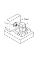
図4に本実施の形態に用いるXYCの3軸NC制御加工機の構成を示す。
図4において、5は加工すべき金型、7は回転軸、8は切削工具、9はXYCステージである。なお、このような加工機において、図4とは逆に切削工具8を回転軸7に取り付け、金型5をXYCステージに取り付けるようにしてもよいが、本実施の形態では図4のように構成したもの用いた。その際、金型6を取り付けた加工機の回転軸7を毎分3000回転で回転させると共に、XYCステージ9をプログラム制御により、毎分0.3mmの速度で移動させ、図1に示す切削加工工程により格子面を加工した。
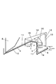
図1に示された11〜18の符号は上記切削加工における各工程(以下、これを工程11〜工程18という)を示すものであり、各工程に示された矢印位置まで工具刃先が移動される。本発明の実施の形態における回折光学素子の製造方法においては、これらの工程を経て、格子頂点にバリのない、所望の正確な回折格子形状を有する回折光学素子が切削加工される。
Next, a method for manufacturing a diffractive optical element molding die in the embodiment of the present invention will be described.
FIG. 4 shows the configuration of an XYC three-axis NC control machine used in the present embodiment.
In FIG. 4, 5 is a mold to be processed, 7 is a rotating shaft, 8 is a cutting tool, and 9 is an XYC stage. In such a processing machine, the
Reference numerals 11 to 18 shown in FIG. 1 indicate the respective steps in the cutting process (hereinafter referred to as steps 11 to 18), and the tool edge is moved to the arrow position indicated in each step. The In the method of manufacturing a diffractive optical element according to the embodiment of the present invention, a diffractive optical element having a desired accurate diffraction grating shape without a burr at the grating vertex is cut through these steps.
つぎに、この図1を用いて本実施の形態における格子面の切削加工の手順について説明する。
図1において、1はバリが除去された平面による格子頂点形状面(以下、これをバリ除去形状面という)、2及び4は回折格子における回折機能を有する斜面(以下、これを格子面という)、3は垂直面である。また、10は切削工具8の刃先の横切刃である。
ここで、バリ除去形状は、格子面2と垂直面3との間の光軸と垂直方向の幅dと、バリ除去形状面と格子面とのなす角度αで定義する。
(1)まず、工程11において、横切刃10によって角度αが10°以下の格子面2を加工しながら、格子面2を延長した線上における垂直面3から2μmだけ離れた位置(工程11の矢印で示された位置)まで、工具刃先を移動させる。
(2)つぎに、工程12において、上記垂直面3から2μm離れた位置を平行に切り込みながら次の格子面4まで1μmだけ残す位置まで荒加工形状を切削加工しながら、工具刃先を移動させる(工程12の矢印で示された位置)。なお、ここでの荒加工においては次の格子面4まで1μmだけ残すように加工したが、この距離は1μmに限られるものではなく、5μm以下であればよい。
(3)つぎに、工程13において、前記工程12において移動させた位置から工程12の切り込み開始点まで工具刃先を戻す。(工程13の矢印で示された位置)。
(4)つぎに、工程14において、上記工程12の開始点からバリ除去形状面1を延長した直線上を格子面2側に1μmだけ離れた位置まで、工具刃先を移動させる(工程14の矢印で示された位置)。
(5)つぎに、工程15において、上記工具刃先を移動させた格子面側から上記垂直面3側に、前記バリ除去形状面1を延長した直線上を進み、幅1.0μm以下のバリ除去形状1を加工し、垂直面3から1μmだけ離れた位置まで切削しながら、工具刃先を移動させる(工程15の矢印で示された位置)。
(6)つぎに、工程16において、前記工程15において切削した位置から格子頂点が切削される以前において本来あるべき点まで、工具刃先を移動させる(工程16の矢印で示された位置)。
(7)つぎに、工程17において、前記工程16において工具刃先を移動させた位置から垂直面3の底部まで切り込みながら、前記工程15で切削加工したバリ除去加工面1を経て、前記工程12の垂直面の荒加工形状をさらに仕上面形状に切削加工しながら、つぎのの格子面4の加工開始位置まで、工具刃先を移動させる(工程17の矢印で示された位置)。
(8)つぎに、工程18において、前記工程11と同様につぎの格子面4を切削加工し(工程18の矢印で示された位置)、このような一連の工程を繰り返し、表面に光軸を中心とする回転対称形状の回折格子を有する回折光学素子成形用金型を製造する。
なお、以上では回折光学素子成形用金型の製造方法について説明したが、加工すべき回折光学素子の素材6に対して、工具8によって直接回折格子を切削加工して、回折光学素子を形成することができることは、説明するまでもないことである。
Next, the procedure for cutting the lattice plane in the present embodiment will be described with reference to FIG.
In FIG. 1,
Here, the burr removal shape is defined by a width d perpendicular to the optical axis between the
(1) First, in step 11, while the
(2) Next, in
(3) Next, in
(4) Next, in
(5) Next, in
(6) Next, in
(7) Next, in
(8) Next, in
Although the method for manufacturing the diffractive optical element molding die has been described above, the diffractive optical element is formed by directly cutting the diffraction grating with the
上記した本実施の形態の製造方法によれば、工具刃先の磨耗や欠けに影響なく、バリを確実に除去することができ、フレアの発生を抑制することができ、また、成形金型を製造した場合には金型の離型性の改善を図ることが可能となる。
また、本実施の形態の製造方法によれば、非光学有効部面積を最小限に抑えることができ、また、バリ除去加工方法は工具刃先にかかる負荷が少ないため工具の寿命を縮めることがない。
また、バリ除去加工面粗さは、格子面粗さと比べて20%以下に抑えることができる。
また、積層型回折格子を構成するに際して、本実施の形態による回折格子を適用し、複数積層した回折格子の全てを、上記したバリの除去された同じ形状とすることで、設計値次数以外の回折光を低減させ、フレアの発生を抑制することが可能となる。
また、前記格子面の加工に際し、前記横切刃の長さ方向が前記格子面に対し30°以下になるように取り付け、切削すべき回折面と切削工具とを相対的に回転させると共に並進移動させながら、前記格子面の低所から高所に向けて格子形状に沿って加工することで、工具刃先の磨耗に影響を受けない正確な格子面の加工が可能となる。
According to the manufacturing method of the present embodiment described above, it is possible to reliably remove burrs without affecting the wear and chipping of the tool blade edge, to suppress the occurrence of flare, and to manufacture a molding die. In this case, it becomes possible to improve the mold releasability.
Further, according to the manufacturing method of the present embodiment, the area of the non-optical effective portion can be minimized, and the deburring method does not reduce the tool life because the load applied to the tool edge is small. .
Moreover, the burr removal processed surface roughness can be suppressed to 20% or less as compared with the lattice surface roughness.
Further, when configuring the laminated diffraction grating, the diffraction grating according to the present embodiment is applied, and all of the laminated diffraction gratings have the same shape from which the burrs are removed, so that the order other than the design value order It is possible to reduce the diffracted light and suppress the occurrence of flare.
Further, when processing the grating surface, the transverse cutting blade is attached so that the length direction of the horizontal cutting edge is 30 ° or less with respect to the grating surface, and the diffraction surface to be cut and the cutting tool are relatively rotated and translated. In addition, by processing along the lattice shape from the low position to the high position of the lattice surface, it is possible to accurately process the lattice surface without being affected by wear of the tool edge.
以下に、本発明の実施例について説明する。
本実施例においては、図4に示す3軸NC制御加工機を用い、上記実施の形態の回折光学素子成形用金型の製造方法によって、回折光学素子成形用金型を製造した。その際、加工すべき金型6には、金型6の表面には加工層として無電解ニッケルメッキを施し、母材としてプラスチック金型用鋼材を用いた。
ここで、金型6を取り付けた加工機の回転軸7を毎分3000回転で回転させると共に、XYCステージ9をプログラム制御により、毎分0.3mmの速度で移動させ、上記実施の形態の回折光学素子成形用金型の製造方法で説明した工程11〜工程18の手順にしたがって、本実施例の金型と比較例の金型とを製造した。
図2に本実施例で製造した金型の格子頂点におけるバリ除去形状を、また、図3に比較例として製造した金型の格子頂点におけるバリ除去形状を示す。
その結果をつぎの表1に示す。
Examples of the present invention will be described below.
In this example, a diffractive optical element molding die was manufactured by the method for manufacturing a diffractive optical element molding die of the above-described embodiment, using a three-axis NC control processing machine shown in FIG. At that time, the mold 6 to be processed was subjected to electroless nickel plating as a processing layer on the surface of the mold 6 and a plastic mold steel was used as a base material.
Here, the
FIG. 2 shows the deburring shape at the lattice apex of the mold manufactured in this example, and FIG. 3 shows the deburring shape at the lattice apex of the mold manufactured as a comparative example.
The results are shown in Table 1 below.

以上の表1から明らかなように、本実施例によればバリを確実に除去することが可能であり、本実施例のαが5.5°のときは、比較例のαが55.0°の場合に比して、バリ除去面粗さ、非レンズ面幅、工具刃先の欠け、等において優れており、回折効率の劣化を比較例よりも小さくすることが可能となる。 As apparent from Table 1 above, according to the present example, it is possible to reliably remove burrs. When α of this example is 5.5 °, α of the comparative example is 55.0. Compared with the case of 0 °, it is excellent in the burr removal surface roughness, the non-lens surface width, the chip of the tool edge, and the like, and the deterioration of the diffraction efficiency can be made smaller than in the comparative example.
1:バリ除去形状面
2:格子面
3:垂直面
4:格子面
10:切削工具刃先の横切刃
11〜18:切削加工における各工程
d:バリ除去形状における格子面2と垂直面3との間の幅
α:バリ除去形状面と格子面とのなす角度
1: Deburring shape surface 2: Lattice surface 3: Vertical surface 4: Lattice surface 10: Cutting tool cutting edge 11 to 18: Each step in cutting d:
Claims (5)
前記回折格子は、前記格子面と垂直面の間の格子頂点にバリ除去形状面を有し、前記バリ除去形状面は、光軸と垂直方向に1.0μm以下の幅で、前記格子面に対して10°以下の角度をなす平面であることを特徴とする回折光学素子。 A diffractive optical element having a diffraction grating with a grating plane and a vertical plane having a rotationally symmetric shape about the optical axis on the surface ,
The diffraction grating has a burr removal shaped surface in a grid vertex between the grating surface and a vertical surface, the burr removal shape surface, at 1.0 [mu] m or less in the width direction perpendicular to the optical axis, the grating surface A diffractive optical element, which is a plane that forms an angle of 10 ° or less with respect to the angle.
格子面を加工した後、垂直面を荒加工し、
前記荒加工した後、前記格子面に対して10°以下の角度をなすように前記切削工具を前記格子面側から垂直面側に移動して、格子頂点にバリ除去形状面を加工し、
前記バリ除去形状面を加工した後、前記垂直面を仕上げ面形状に加工することを特徴とする回折光学素子の製造方法。 A method for producing a diffractive optical element, wherein a diffractive optical element having a diffraction grating having a grating plane and a vertical plane having a rotationally symmetric shape about the optical axis on a surface is cut using a cutting tool,
After processing the lattice plane, the vertical plane by roughing,
After the roughing, the said cutting tool at an angle of 10 ° or less with respect to the grating plane by moving in a vertical plane side from the grating surface, the burr removal shape surface was pressurized Engineering lattice vertices,
Wherein after processing the burr removal shape surface, a method of manufacturing a diffractive optical element, wherein the Turkey be processed into finished surface shape the vertical plane.
格子面を加工した後、垂直面を荒加工し、
前記荒加工した後、前記格子面に対して10°以下の角度をなすように前記切削工具を前記格子面側から垂直面側に移動して、格子頂点にバリ除去形状面を加工し、
前記バリ除去形状面を加工した後、前記垂直面を仕上げ面形状に加工することを特徴とする回折光学素子成形用金型の製造方法。 Diffraction optics for cutting a diffractive optical element molding die for molding a diffractive optical element having a diffraction grating having a grating plane and a vertical plane with a rotationally symmetrical shape about the optical axis on the surface using a cutting tool A method for manufacturing an element molding die,
After processing the lattice plane, the vertical plane by roughing,
After the rough processing, the cutting tool is moved from the lattice surface side to the vertical surface side so as to form an angle of 10 ° or less with respect to the lattice surface, and the burr removal shape surface is processed at the lattice vertex,
Wherein after processing the burr removal shape surface, the production method of the diffractive optical element molding die, wherein the Turkey be processed into finished surface shape the vertical plane.
Priority Applications (1)
| Application Number | Priority Date | Filing Date | Title |
|---|---|---|---|
| JP2005106205A JP4587172B2 (en) | 2005-04-01 | 2005-04-01 | Diffractive optical element, diffractive optical element manufacturing method, and diffractive optical element molding die manufacturing method |
Applications Claiming Priority (1)
| Application Number | Priority Date | Filing Date | Title |
|---|---|---|---|
| JP2005106205A JP4587172B2 (en) | 2005-04-01 | 2005-04-01 | Diffractive optical element, diffractive optical element manufacturing method, and diffractive optical element molding die manufacturing method |
Publications (3)
| Publication Number | Publication Date |
|---|---|
| JP2006285011A JP2006285011A (en) | 2006-10-19 |
| JP2006285011A5 JP2006285011A5 (en) | 2008-05-15 |
| JP4587172B2 true JP4587172B2 (en) | 2010-11-24 |
Family
ID=37406996
Family Applications (1)
| Application Number | Title | Priority Date | Filing Date |
|---|---|---|---|
| JP2005106205A Expired - Fee Related JP4587172B2 (en) | 2005-04-01 | 2005-04-01 | Diffractive optical element, diffractive optical element manufacturing method, and diffractive optical element molding die manufacturing method |
Country Status (1)
| Country | Link |
|---|---|
| JP (1) | JP4587172B2 (en) |
Families Citing this family (2)
| Publication number | Priority date | Publication date | Assignee | Title |
|---|---|---|---|---|
| JP5010377B2 (en) * | 2007-07-20 | 2012-08-29 | 株式会社東芝 | Diffractive optical element, diffractive optical element molding die, and method of manufacturing diffractive optical element molding die |
| JP6173077B2 (en) * | 2013-07-08 | 2017-08-02 | キヤノン株式会社 | Method for manufacturing blazed diffraction grating and method for manufacturing mold therefor |
Citations (12)
| Publication number | Priority date | Publication date | Assignee | Title |
|---|---|---|---|---|
| JPS5548561A (en) * | 1978-09-28 | 1980-04-07 | Hashimoto Forming Co Ltd | Cutting method of foreign material produced in level different surface part and its device |
| JPS5667822A (en) * | 1979-11-07 | 1981-06-08 | Canon Inc | Focal diaphragm |
| JPS57161843A (en) * | 1981-03-31 | 1982-10-05 | Canon Inc | Focusing glass |
| JPH081403A (en) * | 1994-06-22 | 1996-01-09 | Fukui Seisakusho:Kk | Method for deburring of screw end part by machine tool having nc device |
| JPH09127322A (en) * | 1995-08-29 | 1997-05-16 | Olympus Optical Co Ltd | Diffraction optical element |
| JPH1110401A (en) * | 1997-04-21 | 1999-01-19 | Asahi Optical Co Ltd | Working method for zonal lens forming die and cutting tool therefor |
| JPH11188502A (en) * | 1997-12-24 | 1999-07-13 | Isuzu Motors Ltd | Cutting method for different metal composite product |
| JPH11197902A (en) * | 1997-12-29 | 1999-07-27 | Canon Inc | Manufacture of diffractive surface form |
| JP2000263310A (en) * | 1999-03-19 | 2000-09-26 | Canon Inc | Processing method of optical element and processing method of forming die |
| JP2002189114A (en) * | 2000-10-02 | 2002-07-05 | Konica Corp | Optical element, metallic mold and tool |
| JP2002350622A (en) * | 2001-05-25 | 2002-12-04 | Canon Inc | Diffraction optical element and method for turning the same |
| JP2005040912A (en) * | 2003-07-24 | 2005-02-17 | Takamatsu Machinery Co Ltd | Machining device |
-
2005
- 2005-04-01 JP JP2005106205A patent/JP4587172B2/en not_active Expired - Fee Related
Patent Citations (12)
| Publication number | Priority date | Publication date | Assignee | Title |
|---|---|---|---|---|
| JPS5548561A (en) * | 1978-09-28 | 1980-04-07 | Hashimoto Forming Co Ltd | Cutting method of foreign material produced in level different surface part and its device |
| JPS5667822A (en) * | 1979-11-07 | 1981-06-08 | Canon Inc | Focal diaphragm |
| JPS57161843A (en) * | 1981-03-31 | 1982-10-05 | Canon Inc | Focusing glass |
| JPH081403A (en) * | 1994-06-22 | 1996-01-09 | Fukui Seisakusho:Kk | Method for deburring of screw end part by machine tool having nc device |
| JPH09127322A (en) * | 1995-08-29 | 1997-05-16 | Olympus Optical Co Ltd | Diffraction optical element |
| JPH1110401A (en) * | 1997-04-21 | 1999-01-19 | Asahi Optical Co Ltd | Working method for zonal lens forming die and cutting tool therefor |
| JPH11188502A (en) * | 1997-12-24 | 1999-07-13 | Isuzu Motors Ltd | Cutting method for different metal composite product |
| JPH11197902A (en) * | 1997-12-29 | 1999-07-27 | Canon Inc | Manufacture of diffractive surface form |
| JP2000263310A (en) * | 1999-03-19 | 2000-09-26 | Canon Inc | Processing method of optical element and processing method of forming die |
| JP2002189114A (en) * | 2000-10-02 | 2002-07-05 | Konica Corp | Optical element, metallic mold and tool |
| JP2002350622A (en) * | 2001-05-25 | 2002-12-04 | Canon Inc | Diffraction optical element and method for turning the same |
| JP2005040912A (en) * | 2003-07-24 | 2005-02-17 | Takamatsu Machinery Co Ltd | Machining device |
Also Published As
| Publication number | Publication date |
|---|---|
| JP2006285011A (en) | 2006-10-19 |
Similar Documents
| Publication | Publication Date | Title |
|---|---|---|
| JP5864920B2 (en) | Manufacturing method of diffraction grating | |
| JP5010377B2 (en) | Diffractive optical element, diffractive optical element molding die, and method of manufacturing diffractive optical element molding die | |
| JP5731811B2 (en) | Method for manufacturing blazed diffraction grating and method for manufacturing mold for the same | |
| JP4587172B2 (en) | Diffractive optical element, diffractive optical element manufacturing method, and diffractive optical element molding die manufacturing method | |
| JP4158837B2 (en) | Mold, optical element, mold for molding optical element, and manufacturing method thereof | |
| JP4313686B2 (en) | Manufacturing method of mold for annular optical element | |
| JP2002192417A (en) | Grooving device, and grooving method using the same | |
| JP4339573B2 (en) | End mill using single crystal diamond | |
| JP2004219494A (en) | Manufacturing method of optical element | |
| JP4461371B2 (en) | Machining condition setting method of machine tool, machining condition setting program thereof, and recording medium recording the machining condition setting program | |
| JP4556676B2 (en) | The second relief part processing method of the punching die of the press die | |
| JP5445128B2 (en) | Optical element and method for processing optical element mold | |
| JP6566618B2 (en) | Method for manufacturing mold, method for manufacturing optical member, and method for manufacturing optical apparatus | |
| JP5035763B2 (en) | Processing method | |
| JP4582496B2 (en) | Processing method | |
| JP6602056B2 (en) | Optical element manufacturing method, mold, lens array, image forming apparatus, and image reading apparatus | |
| JP2004188511A (en) | Method of fine groove working, workpiece with fine grooves, and molding | |
| US11433606B2 (en) | Three-dimensional shape processing method | |
| JP2011147983A (en) | Forming tool and method for machining the same | |
| US9372289B2 (en) | Method of manufacturing a diffraction grating | |
| JP2009025655A (en) | Diffraction optical element, die for molding diffraction optical element, and method of manufacturing die for molding diffraction optcial element | |
| JP2006285011A5 (en) | ||
| JP2002350622A (en) | Diffraction optical element and method for turning the same | |
| JPWO2019163630A1 (en) | Mold manufacturing method | |
| JP2003136541A (en) | Method for producing three-dimensional blade plate to be embedded in tire molding mold, and mold for producing the blade plate |
Legal Events
| Date | Code | Title | Description |
|---|---|---|---|
| A521 | Request for written amendment filed |
Free format text: JAPANESE INTERMEDIATE CODE: A523 Effective date: 20080401 |
|
| A621 | Written request for application examination |
Free format text: JAPANESE INTERMEDIATE CODE: A621 Effective date: 20080401 |
|
| A977 | Report on retrieval |
Free format text: JAPANESE INTERMEDIATE CODE: A971007 Effective date: 20100614 |
|
| A131 | Notification of reasons for refusal |
Free format text: JAPANESE INTERMEDIATE CODE: A131 Effective date: 20100618 |
|
| A521 | Request for written amendment filed |
Free format text: JAPANESE INTERMEDIATE CODE: A523 Effective date: 20100806 |
|
| TRDD | Decision of grant or rejection written | ||
| A01 | Written decision to grant a patent or to grant a registration (utility model) |
Free format text: JAPANESE INTERMEDIATE CODE: A01 Effective date: 20100830 |
|
| A01 | Written decision to grant a patent or to grant a registration (utility model) |
Free format text: JAPANESE INTERMEDIATE CODE: A01 |
|
| A61 | First payment of annual fees (during grant procedure) |
Free format text: JAPANESE INTERMEDIATE CODE: A61 Effective date: 20100831 Free format text: JAPANESE INTERMEDIATE CODE: A61 Effective date: 20100906 |
|
| R150 | Certificate of patent or registration of utility model |
Ref document number: 4587172 Country of ref document: JP Free format text: JAPANESE INTERMEDIATE CODE: R150 |
|
| FPAY | Renewal fee payment (event date is renewal date of database) |
Free format text: PAYMENT UNTIL: 20130917 Year of fee payment: 3 |
|
| FPAY | Renewal fee payment (event date is renewal date of database) |
Free format text: PAYMENT UNTIL: 20130917 Year of fee payment: 3 |
|
| FPAY | Renewal fee payment (event date is renewal date of database) |
Free format text: PAYMENT UNTIL: 20130917 Year of fee payment: 3 |
|
| FPAY | Renewal fee payment (event date is renewal date of database) |
Free format text: PAYMENT UNTIL: 20130917 Year of fee payment: 3 |
|
| RD03 | Notification of appointment of power of attorney |
Free format text: JAPANESE INTERMEDIATE CODE: R3D03 |
|
| LAPS | Cancellation because of no payment of annual fees |