JP4574426B2 - Data processing apparatus and data processing method - Google Patents
Data processing apparatus and data processing method Download PDFInfo
- Publication number
- JP4574426B2 JP4574426B2 JP2005123528A JP2005123528A JP4574426B2 JP 4574426 B2 JP4574426 B2 JP 4574426B2 JP 2005123528 A JP2005123528 A JP 2005123528A JP 2005123528 A JP2005123528 A JP 2005123528A JP 4574426 B2 JP4574426 B2 JP 4574426B2
- Authority
- JP
- Japan
- Prior art keywords
- area
- write
- address
- read
- data
- Prior art date
- Legal status (The legal status is an assumption and is not a legal conclusion. Google has not performed a legal analysis and makes no representation as to the accuracy of the status listed.)
- Expired - Fee Related
Links
Images


Description
本発明は、同一メモリ上に読み出し領域と書き込み領域を設定し、読み出し領域から読み出したデータを書き込み領域に書き込むデータ処理装置およびデータ処理方法に関する。 The present invention relates to a data processing apparatus and a data processing method for setting a read area and a write area on the same memory and writing data read from the read area to the write area.
従来より、メモリの記憶領域を有効に使用するために原画像データを読み出しながら圧縮された圧縮画像データを原画像データが記憶されていた領域に上書きして記憶させる方法が提案されている。例えば、メモリの空き容量が無くなった時点で、すでにメモリに記憶されている原画像データに圧縮処理を行って、圧縮画像データを上書き保存することにより、メモリの空き容量を確保することが知られている。(特許文献1参照)
しかしながら、例えばRAW形式の原画像データから画像処理された画像データに対してJPEG圧縮を行う場合には圧縮画像データのサイズが原画像データのサイズよりも大きくなってしまう場合や、一部分に複雑なデータがあった場合には、まだ読み出していない原画像データの領域に圧縮画像データを書き込んでしまう場合がある。 However, for example, when JPEG compression is performed on image data that has been subjected to image processing from raw image data in RAW format, the size of the compressed image data may be larger than the size of the original image data or may be partially complicated. If there is data, the compressed image data may be written in the area of the original image data that has not yet been read.
本発明の目的は、原画像データを読み出して、圧縮画像データを上書きしていくデータ処理装置および方法において、まだ読み出していない原画像データの領域に圧縮画像データを書き込んでしまうことのないデータ処理装置および方法を提供することにある。 An object of the present invention is to provide a data processing apparatus and method for reading original image data and overwriting the compressed image data so that the compressed image data is not written in the area of the original image data that has not yet been read. It is to provide an apparatus and method.
このような課題に鑑み、本発明は、同一メモリ上に読み出し領域と書き込み領域を設定し、読み出し領域から読み出したデータに対して圧縮処理を施し、圧縮処理されたデータを再度書き込み領域に書き込むデータ処理装置であって、読み出し領域と重ならない領域に前記読み出されたデータに対して圧縮処理が施された圧縮データの書き込み領域を設定する書き込み領域設定手段と、設定した書き込み領域に前記圧縮データの書き込みが完了したときの書き込み領域の書き込みアドレスおよび読み出し領域の読み出しアドレスを取得するアドレス取得手段と、
取得した前記書き込みアドレスと前記読み出しアドレスとの差分が所定量以下かどうかを判定する判定手段と、前記書き込みアドレスと前記読み出しアドレスとの差分が所定量以下である場合に、前記書き込み領域設定手段にて設定された前記書き込み領域の先頭アドレスから前記アドレス取得手段によって取得した前記書き込みアドレスまでの圧縮データを記録媒体に転送する転送手段と、前記転送手段によって圧縮データが転送された後、前記書き込み領域設定手段にて設定された前記書き込み領域の先頭アドレスと前記アドレス取得手段によって取得した前記読み出しアドレスに基づいて前記書き込み領域設定手段にて設定された前記書き込み領域に書き込み領域を再設定する書き込み領域再設定手段とを有することを特徴とする。
In view of such a problem, the present invention sets a read area and a write area on the same memory, performs compression processing on the data read from the read area, and writes the compressed data to the write area again. a processor, a writing area setting means for setting a writing area of the compressed data compression processing is applied to the read data in a region that does not overlap the read area, the compressed data write area set Address acquisition means for acquiring the write address of the write area and the read address of the read area when the writing of is completed,
A determination unit that determines whether a difference between the acquired write address and the read address is equal to or less than a predetermined amount, and a difference between the write address and the read address is equal to or less than a predetermined amount, the write area setting unit Transfer means for transferring the compressed data from the head address of the write area set up to the write address acquired by the address acquisition means to the recording medium, and after the compressed data is transferred by the transfer means, the write area Based on the start address of the write area set by the setting means and the read address acquired by the address acquiring means, the write area is reset to the write area set by the write area setting means. And setting means.
最初の書き込み領域を設定する際に、書き込み領域の先頭アドレスを読み出し領域の先頭アドレスよりも前に設定して、設定した書き込み領域に書き込みができなくなったときの読み出し領域の読み出しアドレスを取得し、取得した読み出しアドレスに基づいて書き込み領域を再設定する書き込み領域が設定されるので、まだ読み出していない読み出し領域を書き込み領域に設定することがない。したがって、例えばJPEG圧縮を行う場合には圧縮画像データのサイズが原画像データのサイズよりも大きくなってしまったとしても、まだ読み出していない原画像データの領域に圧縮画像データを書き込んでしまうことがない。 When setting the first write area, set the start address of the write area before the start address of the read area, and acquire the read address of the read area when it becomes impossible to write to the set write area, Since a write area for resetting the write area is set based on the acquired read address, a read area that has not yet been read is not set as the write area. Therefore, for example, when JPEG compression is performed, even if the size of the compressed image data is larger than the size of the original image data, the compressed image data may be written in the area of the original image data that has not yet been read. Absent.
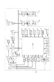
図1は、本発明を実施した画像処理装置の構成を示す図である。 FIG. 1 is a diagram showing the configuration of an image processing apparatus embodying the present invention.
図1において、100は撮像が可能な画像処理装置である。 In FIG. 1, reference numeral 100 denotes an image processing apparatus capable of imaging.
10は撮影レンズ、12は絞り機能を備えるシャッター、14は光学像を電気信号に変換する撮像素子、16は撮像素子14のアナログ信号出力をディジタル信号に変換するA/D変換器である。
18は撮像素子14、A/D変換器16、D/A変換器26にクロック信号や制御信号を供給するタイミング発生回路であり、メモリ制御回路22及びシステム制御回路50により制御される。
A
20は画像処理回路であり、A/D変換器16からのデータ或いはメモリ制御回路22からのデータに対して所定の画素補間処理や色変換処理を行う。オリジナル画像から画像処理パラメータ変換画像の処理もここで行われる。 An image processing circuit 20 performs predetermined pixel interpolation processing and color conversion processing on the data from the A / D converter 16 or the data from the memory control circuit 22. Processing of the image processing parameter converted image from the original image is also performed here.
また、画像処理回路20においては、撮像した画像データを用いて所定の演算処理を行い、得られた演算結果に基づいてシステム制御回路50が露光制御手段40、測距制御手段42に対して制御を行う、TTL(スルー・ザ・レンズ)方式のAF(オートフォーカス)処理、AE(自動露出)処理、EF(フラッシュプリ発光)処理を行っている。 Further, the image processing circuit 20 performs predetermined calculation processing using the captured image data, and the system control circuit 50 controls the exposure control means 40 and the distance measurement control means 42 based on the obtained calculation result. TTL (through-the-lens) AF (autofocus) processing, AE (automatic exposure) processing, and EF (flash pre-emission) processing are performed.
さらに、画像処理回路20においては、撮像した画像データを用いて所定の演算処理を行い、得られた演算結果に基づいてTTL方式のAWB(オートホワイトバランス)処理も行っている。 Further, the image processing circuit 20 performs predetermined arithmetic processing using captured image data, and also performs TTL AWB (auto white balance) processing based on the obtained arithmetic result.
22はメモリ制御回路であり、A/D変換器16、タイミング発生回路18、画像処理回路20、画像表示メモリ24、D/A変換器26、メモリ30、圧縮・伸長回路32を制御する。
A memory control circuit 22 controls the A / D converter 16, the
A/D変換器16のデータが画像処理回路20、メモリ制御回路22を介して、或いはA/D変換器16のデータが直接メモリ制御回路22を介して、画像表示メモリ24或いはメモリ30に書き込まれる。 The data of the A / D converter 16 is written into the image display memory 24 or the memory 30 via the image processing circuit 20 and the memory control circuit 22 or the data of the A / D converter 16 is directly passed through the memory control circuit 22. It is.
24は画像表示メモリ、26はD/A変換器、28はTFT LCD等から成る画像表示部であり、画像表示メモリ24に書き込まれた表示用の画像データはD/A変換器26を介して画像表示部28により表示される。
画像表示部28を用いて撮像した画像データを逐次表示すれば、電子ファインダー機能を実現することが可能である。
Reference numeral 24 denotes an image display memory, 26 denotes a D / A converter, 28 denotes an image display unit including a TFT LCD, and the image data for display written in the image display memory 24 passes through the D / A converter 26. Displayed by the image display unit 28.
If the image data captured using the image display unit 28 is sequentially displayed, the electronic viewfinder function can be realized.
また、画像表示部28は、システム制御回路50の指示により任意に表示をON/OFFすることが可能であり、表示をOFFにした場合には画像処理装置100の電力消費を大幅に低減することが出来る。 The image display unit 28 can arbitrarily turn on / off the display according to an instruction from the system control circuit 50. When the display is turned off, the power consumption of the image processing apparatus 100 can be greatly reduced. I can do it.
30は撮影した静止画像や動画像を格納するためのメモリであり、所定枚数の静止画像や所定時間の動画像を格納するのに十分な記憶量を備えている。
これにより、複数枚の静止画像を連続して撮影する連写撮影やパノラマ撮影の場合にも、大量の画像書き込みをメモリ30に対して行うことが可能となる。
Reference numeral 30 denotes a memory for storing captured still images and moving images, and has a sufficient storage capacity to store a predetermined number of still images and a predetermined time of moving images.
This makes it possible to write a large amount of images to the memory 30 even in continuous shooting or panoramic shooting in which a plurality of still images are continuously shot.
また、メモリ30はシステム制御回路50の作業領域としても使用することが可能である。 The memory 30 can also be used as a work area for the system control circuit 50.
32は適応離散コサイン変換(ADCT)等により画像データを圧縮伸長する圧縮伸長回路であり、メモリ30に格納された画像を読み込んで圧縮処理或いは伸長処理を行い、処理を終えたデータをメモリ30に書き込む。メモリ30のデータを圧縮・伸長するためにデータを転送したり、圧縮伸張回路32で圧縮・伸張したデータをメモリ30に転送する際にはメモリ制御回路によるDMA(Direct Memory Access)でデータの転送を行うことができる。 A compression / decompression circuit 32 compresses / decompresses image data by adaptive discrete cosine transform (ADCT) or the like, reads an image stored in the memory 30, performs compression processing or decompression processing, and stores the processed data in the memory 30. Write. When data is transferred to compress / decompress data in the memory 30, or when data compressed / decompressed by the compression / decompression circuit 32 is transferred to the memory 30, the data is transferred by DMA (Direct Memory Access) by the memory control circuit. It can be performed.
40は絞り機能を備えるシャッター12を制御する露光制御手段であり、フラッシュ48と連携することによりフラッシュ調光機能も有するものである。 Reference numeral 40 denotes an exposure control means for controlling the shutter 12 having a diaphragm function, and has a flash light control function in cooperation with the flash 48.
42は撮影レンズ10のフォーカシングを制御する測距制御手段、44は撮影レンズ10のズーミングを制御するズーム制御手段、46はバリアである保護手段102の動作を制御するバリア制御手段である。
Reference numeral 42 denotes a distance measuring control means for controlling the focusing of the photographing
48はフラッシュであり、AF補助光の投光機能、フラッシュ調光機能も有する。 A flash 48 has an AF auxiliary light projecting function and a flash light control function.
露光制御手段40、測距制御手段42はTTL方式を用いて制御されており、撮像した画像データを画像処理回路20によって演算した演算結果に基づき、システム制御回路50が露光制御手段40、測距制御手段42に対して制御を行う。 The exposure control means 40 and the distance measurement control means 42 are controlled using the TTL method. Based on the calculation result obtained by calculating the captured image data by the image processing circuit 20, the system control circuit 50 performs the exposure control means 40 and the distance measurement. Control is performed on the control means 42.
50は画像処理装置100全体を制御するシステム制御回路、52はシステム制御回路50の動作用の定数、変数、プログラム等を記憶するメモリである。 Reference numeral 50 denotes a system control circuit that controls the entire image processing apparatus 100, and reference numeral 52 denotes a memory that stores constants, variables, programs, and the like for operation of the system control circuit 50.
54はシステム制御回路50でのプログラムの実行に応じて、文字、画像、音声等を用いて動作状態やメッセージ等を表示する液晶表示装置、スピーカー等の表示部であり、画像処理装置100の操作部近辺の視認し易い位置に単数或いは複数個所設置され、例えばLCDやLED、発音素子等の組み合わせにより構成されている。 Reference numeral 54 denotes a display unit such as a liquid crystal display device or a speaker that displays an operation state or a message using characters, images, sounds, or the like in accordance with execution of a program in the system control circuit 50. One or a plurality of places are provided near the portion where they are easily visible, and are configured by a combination of, for example, an LCD, an LED, a sound generation element, and the like.
また、表示部54は、その一部の機能が光学ファインダー104内に設置されている。 In addition, the display unit 54 is partially installed in the optical viewfinder 104.
表示部54の表示内容のうち、LCD等に表示するものとしては、シングルショット/連写撮影表示、セルフタイマー表示、圧縮率表示、記録画素数表示、記録枚数表示、残撮影可能枚数表示、シャッタースピード表示、絞り値表示、露出補正表示、フラッシュ表示、赤目緩和表示、マクロ撮影表示、ブザー設定表示、時計用電池残量表示、電池残量表示、エラー表示、複数桁の数字による情報表示、記録媒体200及び210の着脱状態表示、通信I/F動作表示、日付け・時刻表示や記録メニュー等がある。 Among the display contents of the display unit 54, what is displayed on the LCD or the like includes single shot / continuous shooting display, self-timer display, compression rate display, number of recorded pixels, number of recorded pixels, number of remaining images that can be captured, shutter Speed display, Aperture value display, Exposure compensation display, Flash display, Red-eye reduction display, Macro shooting display, Buzzer setting display, Clock battery level display, Battery level display, Error display, Multi-digit number information display and recording There are a display state of the media 200 and 210, a communication I / F operation display, a date / time display, a recording menu, and the like.
また、表示部54の表示内容のうち、光学ファインダー104内に表示するものとしては、合焦表示、手振れ警告表示、フラッシュ充電表示、シャッタースピード表示、絞り値表示、露出補正表示、等がある。 Further, among the display contents of the display unit 54, what is displayed in the optical viewfinder 104 includes in-focus display, camera shake warning display, flash charge display, shutter speed display, aperture value display, exposure correction display, and the like.
56は電気的に消去・記録可能な不揮発性メモリであり、例えばEEPROM等が用いられる。 Reference numeral 56 denotes an electrically erasable / recordable nonvolatile memory such as an EEPROM.
60、62、64、66、68及び70は、システム制御回路50の各種の動作指示を入力するための操作手段であり、スイッチやダイアル、タッチパネル、視線検知によるポインティング、音声認識装置等の単数或いは複数の組み合わせで構成される。 Reference numerals 60, 62, 64, 66, 68 and 70 are operation means for inputting various operation instructions of the system control circuit 50, and may be a single unit such as a switch, a dial, a touch panel, pointing by line-of-sight detection, a voice recognition device, or the like. Consists of multiple combinations.
ここで、これらの操作手段の具体的な説明を行う。 Here, a specific description of these operating means will be given.
60はモードダイアルスイッチで、電源オフ、自動撮影モード、撮影モード、パノラマ撮影モード、再生モード、マルチ画面再生・消去モード、PC接続モード等の各機能モードを切り替え設定することが出来る。 Reference numeral 60 denotes a mode dial switch, which can switch and set various function modes such as power-off, automatic shooting mode, shooting mode, panoramic shooting mode, playback mode, multi-screen playback / erase mode, and PC connection mode.
62はシャッタースイッチSW1で、不図示のシャッターボタンの第1ストロークでONとなり、AF(オートフォーカス)処理、AE(自動露出)処理、AWB(オートホワイトバランス)処理、EF(フラッシュプリ発光)処理等の動作開始を指示する。 Reference numeral 62 denotes a shutter switch SW1, which is turned ON by a first stroke of a shutter button (not shown), and includes AF (auto focus) processing, AE (automatic exposure) processing, AWB (auto white balance) processing, EF (flash pre-flash) processing, and the like. Instruct the start of operation.
64はシャッタースイッチSW2で、不図示のシャッターボタンの第1ストロークに続く第2ストロークでONとなり、撮像素子12から読み出した信号をA/D変換器16、メモリ制御回路22を介してメモリ30に画像データを書き込む露光処理、画像処理回路20やメモリ制御回路22での演算を用いた現像処理、メモリ30から画像データを読み出し、圧縮・伸長回路32で圧縮を行い、記録媒体200或いは210に画像データを書き込む記録処理という一連の処理の動作開始を指示する。 A shutter switch SW2 64 is turned on in a second stroke following a first stroke of a shutter button (not shown), and a signal read from the image sensor 12 is transferred to the memory 30 via the A / D converter 16 and the memory control circuit 22. Exposure processing for writing image data, development processing using computations in the image processing circuit 20 and the memory control circuit 22, reading out the image data from the memory 30, compression in the compression / decompression circuit 32, and recording on the recording medium 200 or 210 It instructs the start of a series of processes called recording processes for writing data.
66は画像表示ON/OFFスイッチで、画像表示部28のON/OFFを設定することが出来る。 Reference numeral 66 denotes an image display ON / OFF switch that can set ON / OFF of the image display unit 28.
この機能により、光学ファインダー104を用いて撮影を行う際に、TFT LCD等から成る画像表示部への電流供給を遮断することにより、省電力を図ることが可能となる。 With this function, when photographing is performed using the optical viewfinder 104, it is possible to save power by cutting off the current supply to the image display unit including a TFT LCD or the like.
68はクイックレビューON/OFFスイッチで、撮影直後に撮影した画像データを自動再生するクイックレビュー機能を設定する。 Reference numeral 68 denotes a quick review ON / OFF switch, which sets a quick review function for automatically reproducing image data taken immediately after photographing.
70は各種ボタンやタッチパネル等からなる操作部で、メニューボタン、セットボタン、マクロボタン、マルチ画面再生改ページボタン、フラッシュ設定ボタン、単写/連写/セルフタイマー切り替えボタン、メニュー移動+(プラス)ボタン、メニュー移動−(マイナス)ボタン、再生画像移動+(プラス)ボタン、再生画像−(マイナス)ボタン、撮影画質選択ボタン、露出補正ボタン、日付/時間設定ボタン等がある。 Reference numeral 70 denotes an operation unit composed of various buttons, a touch panel, and the like. A menu button, a set button, a macro button, a multi-screen playback page break button, a flash setting button, a single shooting / continuous shooting / self-timer switching button, menu movement + (plus) Button, menu shift- (minus) button, playback image shift + (plus) button, playback image- (minus) button, shooting image quality selection button, exposure correction button, date / time setting button, and the like.
80は電源制御手段で、電池検出回路、DC−DCコンバータ、通電するブロックを切り替えるスイッチ回路等により構成されており、電池の装着の有無、電池の種類、電池残量の検出を行い、検出結果及びシステム制御回路50の指示に基づいてDC−DCコンバータを制御し、必要な電圧を必要な期間、記録媒体を含む各部へ供給する。 Reference numeral 80 denotes a power supply control means, which includes a battery detection circuit, a DC-DC converter, a switch circuit for switching a block to be energized, etc., and detects the presence / absence of a battery, the type of battery, the remaining battery level, and the detection result In addition, the DC-DC converter is controlled based on an instruction from the system control circuit 50, and a necessary voltage is supplied to each unit including the recording medium for a necessary period.
82はコネクタ、84はコネクタ、86はアルカリ電池やリチウム電池等の一次電池やNiCd電池やNiMH電池、Li電池等の二次電池、ACアダプター等からなる電源手段である。 Reference numeral 82 denotes a connector, 84 denotes a connector, and 86 denotes a primary battery such as an alkaline battery or a lithium battery, a secondary battery such as a NiCd battery, a NiMH battery, or a Li battery, an AC adapter, or the like.
90及び94はメモリカードやハードディスク等の記録媒体とのインタフェース、92及び96はメモリカードやハードディスク等の記録媒体と接続を行うコネクタ、98はコネクタ92及び或いは96に記録媒体200或いは210が装着されているか否かを検知する記録媒体着脱検知手段である。 90 and 94 are interfaces with a recording medium such as a memory card or a hard disk, 92 and 96 are connectors for connecting to a recording medium such as a memory card or a hard disk, and 98 is a recording medium 200 or 210 attached to the connector 92 or 96. Recording medium attachment / detachment detecting means for detecting whether or not the recording medium is present.
なお、本実施例では記録媒体を取り付けるインターフェース及びコネクタを2系統持つものとして説明している。もちろん、記録媒体を取り付けるインターフェース及びコネクタは、単数或いは複数、いずれの系統数を備える構成としても構わない。また、異なる規格のインターフェース及びコネクタを組み合わせて備える構成としても構わない。 In this embodiment, it is assumed that there are two interfaces and connectors for attaching the recording medium. Of course, the interface and the connector for attaching the recording medium may have a single or a plurality of systems and any number of systems. Moreover, it is good also as a structure provided with combining the interface and connector of a different standard.
インターフェース及びコネクタとしては、PCMCIAカードやCF(コンパクトフラッシュ(登録商標))カード等の規格に準拠したものを用いて構成して構わない。 The interface and connector may be configured using a PCMCIA card, a CF (Compact Flash (registered trademark)) card, or the like that conforms to a standard.
さらに、インターフェース90及び94、そしてコネクタ92及び96をPCMCIAカードやCF(コンパクトフラッシュ(登録商標))カード等の規格に準拠したものを用いて構成した場合、LANカードやモデムカード、USBカード、IEEE1394カード、P1284カード、SCSIカード、PHS等の通信カード、等の各種通信カードを接続することにより、他のコンピュータやプリンタ等の周辺機器との間で画像データや画像データに付属した管理情報を転送し合うことが出来る。 Further, when the interfaces 90 and 94 and the connectors 92 and 96 are configured using a PCMCIA card, a CF (Compact Flash (registered trademark)) card, or the like, a LAN card, a modem card, a USB card, IEEE1394. Image data and management information attached to image data are transferred to and from peripheral devices such as other computers and printers by connecting various communication cards such as cards, P1284 cards, SCSI cards, and PHS communication cards. I can meet each other.
102は、画像処理装置100のレンズ10を含む撮像部を覆う事により、撮像部の汚れや破損を防止するバリアである保護手段である。
Reference numeral 102 denotes protection means that is a barrier that prevents the imaging unit from being soiled or damaged by covering the imaging unit including the
104は光学ファインダーであり、画像表示部28による電子ファインダー機能を使用すること無しに、光学ファインダーのみを用いて撮影を行うことが可能である。また、光学ファインダー104内には、表示部54の一部の機能、例えば、合焦表示、手振れ警告表示、フラッシュ充電表示、シャッタースピード表示、絞り値表示、露出補正表示などが設置されている。 Reference numeral 104 denotes an optical viewfinder, which can perform photographing using only the optical viewfinder without using the electronic viewfinder function of the image display unit 28. In the optical viewfinder 104, some functions of the display unit 54, for example, a focus display, a camera shake warning display, a flash charge display, a shutter speed display, an aperture value display, an exposure correction display, and the like are installed.
110は通信手段で、RS232CやUSB、IEEE1394、P1284、SCSI、モデム、LAN、無線通信、等の各種通信機能を有する。 A communication unit 110 has various communication functions such as RS232C, USB, IEEE1394, P1284, SCSI, modem, LAN, and wireless communication.
112は通信手段110により画像処理装置100を他の機器と接続するコネクタ或いは無線通信の場合はアンテナである。 Reference numeral 112 denotes a connector for connecting the image processing apparatus 100 to another device by the communication unit 110 or an antenna in the case of wireless communication.
200はメモリカードやハードディスク等の記録媒体である。 Reference numeral 200 denotes a recording medium such as a memory card or a hard disk.
記録媒体200は、半導体メモリや磁気ディスク等から構成される記録部202、画像処理装置100とのインターフェース204、画像処理装置100と接続を行うコネクタ206を備えている。
The recording medium 200 includes a
210はメモリカードやハードディスク等の記録媒体である。 Reference numeral 210 denotes a recording medium such as a memory card or a hard disk.
記録媒体210は、半導体メモリや磁気ディスク等から構成される記録部212、画像処理装置100とのインターフェース214、画像処理装置100と接続を行うコネクタ216を備えている。 The recording medium 210 includes a recording unit 212 composed of a semiconductor memory, a magnetic disk, or the like, an interface 214 with the image processing apparatus 100, and a connector 216 that connects to the image processing apparatus 100.
画像処理装置100の動作を図2および図3を用いて説明する。 The operation of the image processing apparatus 100 will be described with reference to FIGS.
図2は、メモリ30に記録された原画像データに圧縮画像データを上書きしていくときの動作を説明するフローチャートである。図3はメモリ30のデータの配置を説明する図である。 FIG. 2 is a flowchart for explaining the operation when the compressed image data is overwritten on the original image data recorded in the memory 30. FIG. 3 is a diagram for explaining the arrangement of data in the memory 30.
まず、圧縮伸張回路32に対し諸設定を行う(S201)。その後、メモリ30から圧縮伸張回路32に原画像データを読み出すためのReadのDMA設定と、圧縮伸張回路32からメモリに圧縮データを書き込むためのWriteのDMA設定とを行う(S202)。 First, various settings are made for the compression / decompression circuit 32 (S201). Thereafter, the Read DMA setting for reading the original image data from the memory 30 to the compression / decompression circuit 32 and the Write DMA setting for writing the compressed data from the compression / decompression circuit 32 to the memory are performed (S202).
WriteのDMA設定は、書き込み領域の先頭アドレスおよび書き込み量(書き込み領域のサイズ)を設定する。書き込み領域の先頭アドレスは読み出し領域の先頭アドレスよりも前のアドレスになるように設定する。また、設定した書き込み量に達したときに、割り込み処理を発生させるとともに書き込み完了フラグを立てるように設定する。なお、ブロック単位で書き込み処理を行う場合には、設定した書き込み量と実際に書き込み処理を行った書き込み量が完全一致しない場合があるので、次のブロックを書き込むと設定した書き込み量を超えてしまうときに、割り込み処理を発生させるとともに書き込み完了フラグを立てるように設定する。 The write DMA setting sets the start address of the write area and the write amount (size of the write area). The start address of the write area is set to be an address before the start address of the read area. Also, when the set write amount is reached, an interrupt process is generated and a write completion flag is set. Note that when writing processing is performed in units of blocks, the set writing amount may not completely match the writing amount that has actually been written, so writing the next block will exceed the set writing amount. Sometimes, an interrupt process is generated and a write completion flag is set.
ReadのDMA設定は、読み出し領域の先頭アドレスおよび読み出し量(読み出し領域のサイズ)を設定する。設定した読み出し量に達したとき、すなわち、原画像データをすべて読み出しときに、割り込み処理を発生させるとともに読み出し完了フラグを立てるように設定する。 The DMA setting for Read sets the start address of the read area and the read amount (read area size). When the set read amount is reached, that is, when all the original image data is read, an interrupt process is generated and a read completion flag is set.
図3(a)はステップS202にて設定される書き込み領域と読み出し領域を示す図である。図3(a)において、原画像データはアドレス0C0000H〜FFFFFFHの領域に記録されている。したがってReadのDMA設定で設定される読み出し領域はアドレス0C0000H〜FFFFFFHの領域(図中のReadで示される領域)となる。一方、WriteのDMA設定で設定される書き込み領域は、読み出し領域の先頭アドレス0C0000Hより前アドレスである0A0000Hを設定する。書き込み量は0A0000Hから原画像データが記録されている領域の先頭アドレス0C0000Hの差分を設定する。すなわち、本実施形態では0A0000Hと0C0000Hとの差分である128KBを書き込み量に設定する。図3(a)では領域1が書き込み領域として設定される。 FIG. 3A shows the write area and read area set in step S202. In FIG. 3A, the original image data is recorded in the area of addresses 0C0000H to FFFFFFH. Therefore, the read area set by the Read DMA setting is an area of addresses 0C0000H to FFFFFFH (area indicated by Read in the drawing). On the other hand, the write area set by the write DMA setting is set to 0A0000H, which is an address before the start address 0C0000H of the read area. The write amount is set to a difference from 0A0000H to the start address 0C0000H of the area where the original image data is recorded. That is, in this embodiment, 128 KB, which is the difference between 0A0000H and 0C0000H, is set as the write amount. In FIG. 3A, the area 1 is set as the writing area.
ReadおよびWriteのDMA設定をして、ステップS203に進む。ステップS203では、読み出し領域の先頭アドレス0C0000Hから順に原画像データを読み出し、圧縮伸張回路32にて圧縮処理を行った後、書き込み領域の先頭アドレス0A0000Hから圧縮画像データを書き込んでいく。ステップS204では、書き込み領域への書き込みが設定した書き込み量に達した(書き込み完了)場合、もしくは読み出し領域からの読み出しが設定された読み出し量に達した(読み出し完了)場合に発生する割り込み処理があるかどうかを判定し、割り込み処理が発生すればステップS205に進み、発生しなければステップS204を繰り返す。 Set the DMA of Read and Write, and proceed to Step S203. In step S203, the original image data is read sequentially from the read area start address 0C0000H, and after compression processing by the compression / decompression circuit 32, the compressed image data is written from the write area start address 0A0000H. In step S204, there is an interrupt process that occurs when writing to the writing area reaches the set writing amount (writing completion) or when reading from the reading area reaches the setting reading amount (reading completion). If interrupt processing occurs, the process proceeds to step S205, and if not, step S204 is repeated.
ステップS205では発生した割り込み処理が、読み出し領域からの読み出し完了なのかどうかを判定する。ここで、読み出し領域からの読み出し完了と判定される場合には処理を終了する。一方、設定した書き込み領域への書き込み完了と判定された場合には、ステップS206に進む。 In step S205, it is determined whether or not the interrupt processing that has occurred is completion of reading from the reading area. Here, when it is determined that the reading from the reading area is completed, the process ends. On the other hand, if it is determined that the writing to the set writing area is completed, the process proceeds to step S206.
ステップS206では、割り込み処理が発生したときの書き込みアドレスと読み出しアドレスを取得する。ここで、書き込みアドレスとは、書き込み領域への書き込み処理が設定した書き込み量に達したときの書き込み領域の終端アドレスである。ブロック単位で書き込み処理を行っている場合には最後の書き込み処理を行った終端アドレスとなる。 In step S206, the write address and read address when the interrupt process occurs are acquired. Here, the write address is the end address of the write area when the write amount to the write area reaches the set write amount. When the writing process is performed in block units, it is the end address at which the last writing process was performed.
読み出しアドレスとは、書き込み処理が書き込み領域の終端アドレスに達したときの読み出し領域のアドレスである。つまり、読み出しアドレスは、書き込み領域の終端まで書き込んだときに読み出し領域をどこまで読み出したのかを示している。 The read address is the address of the read area when the write process reaches the end address of the write area. That is, the read address indicates how far the read area has been read when writing to the end of the write area.
そして、読み出しアドレスと書き込みアドレスとの差で示される容量が所定の容量を上回るかどうかを判定する。読み出しアドレスと書き込みアドレスとの差は、設定した書き込み領域がいっぱいになるまでに、どのくらいの読み出しを行ったかどうかを表している。 Then, it is determined whether or not the capacity indicated by the difference between the read address and the write address exceeds a predetermined capacity. The difference between the read address and the write address represents how much data has been read before the set write area is full.
図3(a)で説明すると、書き込み領域に設定されている領域1がいっぱいになったときに、読出し領域はアドレス0DFFFFHまで読み出している。このとき、領域1の終端アドレスが0BFFFFHであった場合には、0DFFFFHと0BFFFFHとの差で示される容量が所定の容量(例えば100KB)を上回るかどうかを判定する。 Referring to FIG. 3A, when the area 1 set as the write area becomes full, the read area reads to the address 0DFFFFH. At this time, if the end address of region 1 is 0BFFFFH, it is determined whether or not the capacity indicated by the difference between 0DFFFFH and 0BFFFFH exceeds a predetermined capacity (for example, 100 KB).
ここで、読み出しアドレスと書き込みアドレスとの差で示される容量が所定の容量を上回る場合にはステップS211に進み、読み出しアドレスと書き込みアドレスとの差で示される容量が所定の容量以下の場合にはステップS208に進む。 If the capacity indicated by the difference between the read address and the write address exceeds a predetermined capacity, the process proceeds to step S211. If the capacity indicated by the difference between the read address and the write address is equal to or less than the predetermined capacity, the process proceeds to step S211. Proceed to step S208.
まず、読み出しアドレスと書き込みアドレスとの差で示される容量が所定の容量を上回る場合について説明する。 First, a case where the capacity indicated by the difference between the read address and the write address exceeds a predetermined capacity will be described.
ステップS211では、新たにWriteのDMA設定を行う。ここでは、前回の圧縮転送処理にて読み出しが完了している読み出し領域が新たな書き込み領域となるようにWriteのDMA設定を行う。 In step S211, a new DMA setting of Write is performed. Here, the write DMA setting is performed so that the read area that has been read in the previous compression transfer process becomes a new write area.
図3(a)および図3(b)にて説明する。図3(a)において、1回目のWriteのDMA設定にて、領域1(0A0000H〜0BFFFFH)を書き込み領域に設定し、読み出し領域のうち領域2(0C0000H〜0DFFFFH)に記録されている原画像データを圧縮転送処理した。2回目のWriteのDMA設定では、図3(b)のように、領域2(0C0000H〜0DFFFFH)を新たな書き込み領域に設定する。このようにWriteのDMA設定を行ってステップS210に進む。 This will be described with reference to FIGS. 3 (a) and 3 (b). In FIG. 3A, in the first Write DMA setting, area 1 (0A0000H to 0BFFFFH) is set as a writing area, and original image data recorded in area 2 (0C0000H to 0DFFFFH) in the reading area. Compressed and transferred. In the second Write DMA setting, area 2 (0C0000H to 0DFFFFH) is set as a new writing area, as shown in FIG. 3B. In this way, Write DMA setting is performed, and the process proceeds to step S210.
ステップS210では、ステップS206で取得した読み出しアドレスの次のアドレスから原画像データの読み出しを開始して、圧縮伸張回路32にて圧縮処理を行った後、新たに設定した書き込み領域の先頭アドレスから圧縮画像データを書き込んでいく。 In step S210, reading of the original image data is started from the address next to the read address acquired in step S206, compression is performed by the compression / decompression circuit 32, and compression is performed from the head address of the newly set write area. Write the image data.
図3(b)で説明すると、ステップS206で取得した読み出しアドレス0DFFFFHの次のアドレス0E0000Hから原画像データの読み出しを開始して、新たに書き込み領域に設定された領域2(0C0000H〜0DFFFFH)に圧縮画像データを書き込んでいき、ステップS204に戻る。 Referring to FIG. 3B, reading of the original image data starts from the address 0E0000H next to the read address 0DFFFFH acquired in step S206, and is compressed to the area 2 (0C0000H to 0DFFFFH) newly set as the writing area. The image data is written, and the process returns to step S204.
領域2に設定した書き込み量を書き込んだ場合には、再度割り込み処理が発生する。割り込み処理が発生したときに、読み出しアドレスが領域3の終端アドレスの原画像データを読み出していたとすると、領域2の終端アドレス0DFFFFHと、領域3の終端アドレス0FFFFFHとを比較する。0DFFFFHとFFFFFHの差で示される容量が所定の容量を上回る場合には、図3(c)のように、領域3を次の書き込み領域としてWriteのDMA設定で設定して、領域4の先頭から読み出しを行う。 When the write amount set in the area 2 is written, interrupt processing occurs again. If the original image data whose read address is the end address of the area 3 is read when the interrupt processing occurs, the end address 0DFFFFH of the area 2 is compared with the end address 0FFFFFH of the area 3. When the capacity indicated by the difference between 0DFFFFH and FFFFFH exceeds the predetermined capacity, the area 3 is set as the next writing area by the write DMA setting as shown in FIG. Read.
ステップS204〜ステップS211までの処理を繰り返して、読み出し領域のすべての原画像データが読み出されると割り込み処理が発生する。読み出し領域からの読み出し完了の割り込み処理であることがステップS205で判定されると、このフローチャートは終了する。 When the processing from step S204 to step S211 is repeated and all the original image data in the read area is read, an interrupt process occurs. If it is determined in step S205 that the interrupt process is complete when reading from the read area, the flowchart ends.
次に、読み出しアドレスと書き込みアドレスとの差で示される容量が所定の容量以下の場合について説明する。 Next, a case where the capacity indicated by the difference between the read address and the write address is equal to or less than a predetermined capacity will be described.
図3(c)において、領域3に設定した書き込み量を書き込み、再度割り込み処理が発生する。割り込み処理が発生したときに、読み出しアドレスが領域4の終端アドレスの原画像データを読み出していたとすると、ステップS206にて領域3の終端アドレス0FFFFFHと、領域4の終端アドレス103FFFHとを比較する。0FFFFFHと103FFFHの差で示される容量は所定の容量(100KB)以下であるのでステップS208に進む。 In FIG. 3C, the write amount set in area 3 is written, and interrupt processing occurs again. If the original image data whose read address is the end address of the area 4 is read when the interrupt process occurs, the end address 0FFFFFH of the area 3 is compared with the end address 103FFFH of the area 4 in step S206. Since the capacity indicated by the difference between 0FFFFFH and 103FFFH is equal to or less than the predetermined capacity (100 KB), the process proceeds to step S208.
ステップS208では、記録されている圧縮画像データをすべて記録媒体200または記録媒体210に移動して、ステップS209に進む。図3(c)では、領域1、2、3に記録されている圧縮画像データをすべて記録媒体200または記録媒体210に移動する。 In step S208, all the recorded compressed image data is moved to the recording medium 200 or the recording medium 210, and the process proceeds to step S209. In FIG. 3C, all the compressed image data recorded in the areas 1, 2, and 3 are moved to the recording medium 200 or the recording medium 210.
ステップS209では、再度WriteのDMA設定を行う。ここでは、ステップS202で最初に書き込み領域として設定した領域の開始アドレスからステップS206にて取得した読み出しアドレスまでを新たな書き込み領域として設定する。図3(d)で説明すると、領域1の先頭アドレス0A0000Hから領域4の終端アドレス103FFFHまでの領域を書き込み領域として設定する。 In step S209, Write DMA setting is performed again. Here, a new write area is set from the start address of the area initially set as the write area in step S202 to the read address acquired in step S206. Referring to FIG. 3D, the area from the start address 0A0000H of area 1 to the end address 103FFFH of area 4 is set as the write area.
ステップS204〜ステップS211までの処理繰り返して、読み出し領域のすべての原画像データが読み出されると割り込み処理が発生する。読み出し領域からの読み出し完了の割り込み処理であることがステップS205で判定されると、このフローチャートは終了する。 When all of the original image data in the reading area is read by repeating the processing from step S204 to step S211, interrupt processing occurs. If it is determined in step S205 that the interrupt process is complete when reading from the read area, the flowchart ends.
このように書き込み領域が設定されるので、書き込みアドレスが読み出しアドレスを追い越すことがない。また、書き込みアドレスと読み出しアドレスの差分で示される容量が所定の容量に近づいたら、メモリ30に記録されている画像圧縮データをすべて記憶媒体200、210に移動させた後、原画像データの圧縮を再開するので、処理の途中で書き込み領域が不足することもない。 Since the write area is set in this way, the write address does not overtake the read address. When the capacity indicated by the difference between the write address and the read address approaches a predetermined capacity, all the compressed image data recorded in the memory 30 is moved to the storage media 200 and 210, and then the original image data is compressed. Since the process is resumed, there is no shortage of the writing area during the process.
30 メモリ
32 画像圧縮伸長回路
50 システム制御回路
200 記録媒体
210 記録媒体
30 memory 32 image compression / decompression circuit 50 system control circuit 200 recording medium 210 recording medium
Claims (4)
読み出し領域と重ならない領域に前記読み出されたデータに対して圧縮処理が施された圧縮データの書き込み領域を設定する書き込み領域設定手段と、
設定した書き込み領域に前記圧縮データの書き込みが完了したときの書き込み領域の書き込みアドレスおよび読み出し領域の読み出しアドレスを取得するアドレス取得手段と、
取得した前記書き込みアドレスと前記読み出しアドレスとの差分が所定量以下かどうかを判定する判定手段と、
前記書き込みアドレスと前記読み出しアドレスとの差分が所定量以下である場合に、前記書き込み領域設定手段にて設定された前記書き込み領域の先頭アドレスから前記アドレス取得手段によって取得した前記書き込みアドレスまでの圧縮データを記録媒体に転送する転送手段と、
前記転送手段によって圧縮データが転送された後、前記書き込み領域設定手段にて設定された前記書き込み領域の先頭アドレスと前記アドレス取得手段によって取得した前記読み出しアドレスに基づいて前記書き込み領域設定手段にて設定された前記書き込み領域に書き込み領域を再設定する書き込み領域再設定手段とを有することを特徴とするデータ処理装置。 A data processing apparatus that sets a read area and a write area on the same memory, performs compression processing on data read from the read area, and writes the compressed data to the write area again .
A write area setting means for setting a write area for compressed data obtained by performing compression processing on the read data in an area that does not overlap with a read area;
Address acquisition means for acquiring the write address of the write area and the read address of the read area when the writing of the compressed data is completed in the set write area;
Determining means for determining whether or not a difference between the acquired write address and the read address is equal to or less than a predetermined amount;
When the difference between the write address and the read address is a predetermined amount or less, the compressed data from the start address of the write area set by the write area setting means to the write address acquired by the address acquisition means Transfer means for transferring to a recording medium;
After the compressed data is transferred by the transfer means, the write area setting means sets based on the start address of the write area set by the write area setting means and the read address acquired by the address acquisition means And a write area resetting means for resetting a write area in the written area.
読み出し領域と重ならない領域に前記読み出されたデータに対して圧縮処理が施された圧縮データの書き込み領域を設定する書き込み領域設定工程と、
設定した書き込み領域に前記圧縮データの書き込みが完了したときの書き込み領域の書き込みアドレスおよび読み出し領域の読み出しアドレスを取得するアドレス取得工程と、
取得した前記書き込みアドレスと前記読み出しアドレスとの差分が所定量以下かどうかを判定する判定工程と、
前記書き込みアドレスと前記読み出しアドレスとの差分が所定量以下である場合に、前記書き込み領域設定工程にて設定された前記書き込み領域の先頭アドレスから前記アドレス取得手段によって取得した前記書き込みアドレスまでの圧縮データを記録媒体に転送する転送工程と、
前記転送工程によって圧縮データが転送された後、前記書き込み領域設定工程にて設定された前記書き込み領域の先頭アドレスと前記アドレス取得工程によって取得した前記読み出しアドレスに基づいて書き込み領域を前記書き込み領域設定工程にて設定された前記書き込み領域に再設定する書き込み領域再設定工程とを有することを特徴とするデータ処理方法。 A data processing method that sets a read area and a write area on the same memory, performs compression processing on data read from the read area, and writes the compressed data to the write area again .
A writing area setting step for setting a writing area for compressed data in which compression processing is performed on the read data in an area that does not overlap with a reading area;
An address acquisition step of acquiring a write address of the write area and a read address of the read area when writing of the compressed data is completed in the set write area;
A determination step of determining whether a difference between the acquired write address and the read address is equal to or less than a predetermined amount;
When the difference between the write address and the read address is a predetermined amount or less, the compressed data from the start address of the write area set in the write area setting step to the write address acquired by the address acquisition unit Transferring to the recording medium;
After the compressed data is transferred in the transfer step, the write region is set in the write region based on the start address of the write region set in the write region setting step and the read address acquired in the address acquisition step And a writing area resetting step for resetting the writing area set in step (1).
Priority Applications (1)
| Application Number | Priority Date | Filing Date | Title |
|---|---|---|---|
| JP2005123528A JP4574426B2 (en) | 2005-04-21 | 2005-04-21 | Data processing apparatus and data processing method |
Applications Claiming Priority (1)
| Application Number | Priority Date | Filing Date | Title |
|---|---|---|---|
| JP2005123528A JP4574426B2 (en) | 2005-04-21 | 2005-04-21 | Data processing apparatus and data processing method |
Publications (3)
| Publication Number | Publication Date |
|---|---|
| JP2006303962A JP2006303962A (en) | 2006-11-02 |
| JP2006303962A5 JP2006303962A5 (en) | 2008-06-05 |
| JP4574426B2 true JP4574426B2 (en) | 2010-11-04 |
Family
ID=37471716
Family Applications (1)
| Application Number | Title | Priority Date | Filing Date |
|---|---|---|---|
| JP2005123528A Expired - Fee Related JP4574426B2 (en) | 2005-04-21 | 2005-04-21 | Data processing apparatus and data processing method |
Country Status (1)
| Country | Link |
|---|---|
| JP (1) | JP4574426B2 (en) |
Families Citing this family (2)
| Publication number | Priority date | Publication date | Assignee | Title |
|---|---|---|---|---|
| JP4667348B2 (en) * | 2006-11-20 | 2011-04-13 | シャープ株式会社 | Encoded data memory storage control device, method, and image processing device |
| JP5018060B2 (en) * | 2006-12-14 | 2012-09-05 | 日本電気株式会社 | Information processing apparatus and information processing method |
Citations (5)
| Publication number | Priority date | Publication date | Assignee | Title |
|---|---|---|---|---|
| JPH10230642A (en) * | 1997-02-19 | 1998-09-02 | Konica Corp | Printer |
| JP2000059442A (en) * | 1998-08-06 | 2000-02-25 | Nec Corp | Memory control circuit |
| JP2001195821A (en) * | 2000-01-11 | 2001-07-19 | Matsushita Electric Ind Co Ltd | Device for correcting reproduction speed error |
| JP2001326795A (en) * | 2000-05-15 | 2001-11-22 | Sharp Corp | Image forming device and its memory area allocation method |
| JP2004222069A (en) * | 2003-01-16 | 2004-08-05 | Canon Inc | Image processor |
-
2005
- 2005-04-21 JP JP2005123528A patent/JP4574426B2/en not_active Expired - Fee Related
Patent Citations (5)
| Publication number | Priority date | Publication date | Assignee | Title |
|---|---|---|---|---|
| JPH10230642A (en) * | 1997-02-19 | 1998-09-02 | Konica Corp | Printer |
| JP2000059442A (en) * | 1998-08-06 | 2000-02-25 | Nec Corp | Memory control circuit |
| JP2001195821A (en) * | 2000-01-11 | 2001-07-19 | Matsushita Electric Ind Co Ltd | Device for correcting reproduction speed error |
| JP2001326795A (en) * | 2000-05-15 | 2001-11-22 | Sharp Corp | Image forming device and its memory area allocation method |
| JP2004222069A (en) * | 2003-01-16 | 2004-08-05 | Canon Inc | Image processor |
Also Published As
| Publication number | Publication date |
|---|---|
| JP2006303962A (en) | 2006-11-02 |
Similar Documents
| Publication | Publication Date | Title |
|---|---|---|
| EP1715671A1 (en) | Image sensing apparatus and white balance correction method | |
| JP5424732B2 (en) | Imaging apparatus, control method thereof, and program | |
| JP4891270B2 (en) | Image editing apparatus, image editing method and program | |
| JP2008160792A (en) | Electronic camera and control method thereof | |
| JP2005176136A (en) | Image processor, image reproducing method, program and recording medium | |
| JP2008079137A (en) | Image processing apparatus and control method thereof, computer program, and storage medium | |
| JP2007028070A (en) | Device and method for preserving picture, and control program | |
| JP4533017B2 (en) | Imaging device | |
| JP4324116B2 (en) | Image processing apparatus, control method therefor, program, and storage medium | |
| JP4681937B2 (en) | Imaging apparatus and imaging method | |
| JP4574426B2 (en) | Data processing apparatus and data processing method | |
| JP4700796B2 (en) | Imaging apparatus, control method therefor, and storage medium | |
| JP4574382B2 (en) | Information retrieval apparatus, control method therefor, program, and storage medium | |
| JP2007158604A (en) | Imaging apparatus and its control method | |
| JP2003274366A (en) | Image processor, image processing method, program, and recording medium | |
| JP2011223079A (en) | Image processing apparatus | |
| JP4818158B2 (en) | Image processing apparatus, control method therefor, and computer program | |
| JP4878456B2 (en) | Recording medium and imaging apparatus | |
| JP2007221722A (en) | Image processing apparatus and control method thereof | |
| JP4298534B2 (en) | Image display apparatus and method | |
| JP2004328037A (en) | Imaging and image recording apparatus | |
| JP4766706B2 (en) | Image processing apparatus, control method therefor, program, and storage medium | |
| JP4717762B2 (en) | Image reproducing apparatus, control method for image reproducing apparatus, program, and recording medium | |
| JP4785778B2 (en) | Imaging device, control method thereof, and program | |
| JP2008077402A (en) | Image processor, its control method, computer program and storage medium |
Legal Events
| Date | Code | Title | Description |
|---|---|---|---|
| A521 | Written amendment |
Free format text: JAPANESE INTERMEDIATE CODE: A523 Effective date: 20080418 |
|
| A621 | Written request for application examination |
Free format text: JAPANESE INTERMEDIATE CODE: A621 Effective date: 20080418 |
|
| A977 | Report on retrieval |
Free format text: JAPANESE INTERMEDIATE CODE: A971007 Effective date: 20100128 |
|
| RD04 | Notification of resignation of power of attorney |
Free format text: JAPANESE INTERMEDIATE CODE: A7424 Effective date: 20100201 |
|
| A131 | Notification of reasons for refusal |
Free format text: JAPANESE INTERMEDIATE CODE: A131 Effective date: 20100202 |
|
| A521 | Written amendment |
Free format text: JAPANESE INTERMEDIATE CODE: A523 Effective date: 20100402 |
|
| A02 | Decision of refusal |
Free format text: JAPANESE INTERMEDIATE CODE: A02 Effective date: 20100420 |
|
| RD01 | Notification of change of attorney |
Free format text: JAPANESE INTERMEDIATE CODE: A7421 Effective date: 20100630 |
|
| A521 | Written amendment |
Free format text: JAPANESE INTERMEDIATE CODE: A523 Effective date: 20100708 |
|
| A911 | Transfer of reconsideration by examiner before appeal (zenchi) |
Free format text: JAPANESE INTERMEDIATE CODE: A911 Effective date: 20100728 |
|
| TRDD | Decision of grant or rejection written | ||
| A01 | Written decision to grant a patent or to grant a registration (utility model) |
Free format text: JAPANESE INTERMEDIATE CODE: A01 Effective date: 20100817 |
|
| A01 | Written decision to grant a patent or to grant a registration (utility model) |
Free format text: JAPANESE INTERMEDIATE CODE: A01 |
|
| A61 | First payment of annual fees (during grant procedure) |
Free format text: JAPANESE INTERMEDIATE CODE: A61 Effective date: 20100818 |
|
| R150 | Certificate of patent or registration of utility model |
Free format text: JAPANESE INTERMEDIATE CODE: R150 |
|
| FPAY | Renewal fee payment (event date is renewal date of database) |
Free format text: PAYMENT UNTIL: 20130827 Year of fee payment: 3 |
|
| LAPS | Cancellation because of no payment of annual fees |