JP4549458B2 - DMA transfer device - Google Patents
DMA transfer device Download PDFInfo
- Publication number
- JP4549458B2 JP4549458B2 JP10690399A JP10690399A JP4549458B2 JP 4549458 B2 JP4549458 B2 JP 4549458B2 JP 10690399 A JP10690399 A JP 10690399A JP 10690399 A JP10690399 A JP 10690399A JP 4549458 B2 JP4549458 B2 JP 4549458B2
- Authority
- JP
- Japan
- Prior art keywords
- signal
- mask
- cpu
- dreq
- dma
- Prior art date
- Legal status (The legal status is an assumption and is not a legal conclusion. Google has not performed a legal analysis and makes no representation as to the accuracy of the status listed.)
- Expired - Fee Related
Links
Images


Description
【0001】
【発明の属する技術分野】
本発明は、DMA(Direct Memory Access)転送装置に係り、詳細には、CPUの動作と独立に、メモリと外部リクエストデバイス間で直接データを転送するDMA転送制御を行うDMA制御部を備えたDMA転送装置に関する。
【0002】
【従来の技術】
DMA転送は、CPUを介さずに直接メインメモリとI/O装置(例えば、外部リクエストデバイス)などの周辺機器間でデータ転送を行うものである。これにより高速・大容量のデータ転送がCPUのオーバヘッドを伴わずに可能となる。DMA転送は、一般にDMAC(Direct Memory Access Controler)がバスを管理して転送を制御する。
【0003】
従来、DMACと外部リクエストデバイスとの間でDMA転送を行うシステムにおいて、DMACは、外部リクエストデバイスから出力されるDMAリクエスト(DREQ)信号を受けてメモリデバイスと外部リクエストデバイス間でデータ転送ができるよう他のデバイスを制御する。
【0004】
図32は従来のDMA転送装置の構成を示すブロック図であり、DMACと外部リクエストデバイス間のデータ転送を例としたものである。
【0005】
図32において、1はCPU、2はDMAC、3,4は複数の(2つの)外部リクエストデバイス(外部リクエストデバイス1,2)、5は外部メモリである。
【0006】
外部リクエストデバイス3,4からリクエスト信号DREQ1/DREQ2がDMAC2に対して出力される。DMAC2には、それぞれのDMAリクエスト信号DREQ1/DREQ2が入力され、DMAC2は、このDREQ信号の入力によって、CPU1に対してバスリクエスト(BREQ)信号を出力し、バスの開放を要求する。
【0007】
BREQを受けたCPU1は、バス開放許可(BACK)信号を出力し、バスをDMAC2に開放する。ここで、外部リクエストデバイスが複数存在する場合は、各デバイスからのDREQの発生回数が増加するため、DMACの内部でBREQ信号を発生させる順序を調整(調停)し、各外部リクエストデバイスのDMA転送を実現している。
【0008】
【発明が解決しようとする課題】
しかしながら、このような従来のDMA転送装置にあっては、上述したように複数の外部リクエストデバイスシステムに搭載した場合に、DREQ信号の調停が必要である。また、外部リクエストデバイスの数と外部リクエストデバイスのDREQ信号の発生周期によってDMAによるバスの占有率が大きくなり、通常の一連のCPUによる処理が極端に延ばされてしまう可能性があるという問題点があった。
【0009】
以下、この不具合について説明する。
【0010】
図33はDMACの調停のタイミングを概念的に示すタイミングチャートである。
【0011】
3チャンネル持っているDMACにおいて、各CHの1回のDMA転送に所要する時間をTとする。図33の場合は、DMACが各チャンネルのDMAの調停を行って、CH1→CH2→CH3→CH1といったラウンドロビン型の方式でチャンネルを使用している。しかし、この方法を用いると、DMA転送にだけバスが占有されることになり、プロセッサがバスを使用して処理している時間が、時間的に極端に延ばされてしまうことがある。
【0012】
本発明は、外部リクエストデバイスが複数存在する場合、または、DREQ信号の発生周期が短い外部リクエストデバイスが同一のバスに存在する場合、DMAによるバス占有率を低減し、時間的にバスを有効に利用することができるDMA転送装置を提供することを目的とする。
【0014】
【課題を解決するための手段】
本発明に係るDMA転送装置は、CPUと、外部メモリと、それぞれがデータ転送リクエスト信号を発生させる複数の外部リクエストデバイスと、前記CPUの動作と独立に、前記外部メモリと前記複数の外部リクエストデバイスとの間のDMA転送を制御するDMA制御部と、前記CPU、前記外部メモリ、前記複数の外部リクエストデバイス、及び前記DMA制御部を接続するバスとを備え、
前記DMA制御部は、前記複数の外部リクエストデバイスのいずれかがデータ転送リクエスト信号を発生したときに、前記CPUに対してバス開放リクエスト信号を出力してバスの開放を要求し、前記CPUからバス開放許可信号が返されると、前記データ転送リクエスト信号を発生させた前記外部リクエストデバイスにデータ転送リクエスト確認信号を送出して、前記外部メモリと前記データ転送リクエスト信号を発生させた前記外部リクエストデバイスとの間のDMA転送を制御する手段と、前記DMA転送によるバス占有状態を制御するように前記データ転送リクエスト信号をマスクすることによってバスリクエスト信号を生成するマスク回路と前記データ転送リクエスト信号をマスクするマスク時間をカウントするカウンタとを有し、前記複数の外部リクエストデバイスごとに設けられたマスク手段と、前記マスク手段の前記マスク回路のいずれかによって生成された前記バスリクエスト信号に基づいて、前記DMA転送を制御する手段による前記CPUへの前記バス開放リクエスト信号の出力を調整して、前記DMA転送を調停する調停手段とを有し、
前記CPUは、同時動作可能な前記外部リクエストデバイスの数に応じて前記マスク時間を制御する手段と、前記CPU自身が処理するタスクの処理負荷を管理するタスク管理手段とを有し、
前記タスク管理手段は、前記CPUが処理するタスクごとに設定された前記マスク時間に関する情報を保持する手段と、前記CPUによって現在処理されているタスクを監視する監視手段と、前記監視手段によって監視されている前記タスクに応じて、前記マスク時間に関する情報を保持する手段から、前記マスク時間を選択する選択手段と、選択された前記マスク時間を前記マスク回路が用いるマスク時間として設定する設定手段とを有することを特徴とする。
【0021】
【発明の実施の形態】
第1の実施形態
図1は本発明の第1の実施形態に係るDMA転送装置の構成を示すブロック図である。本実施形態は、外部メモリと外部リクエストデバイスとの間でDMA転送を行うシステムに適用したものである。
【0022】
図1において、DMA転送装置は、CPU100、DMAC110(DMA制御部)、外部リクエストデバイス111、外部リクエストデバイス112、及び外部メモリ113から構成される。
【0023】
DMAC110は、2つのDMAチャンネルを搭載しており、それらをCH0,CH1とする。また、CH0とCH1はそれぞれ、外部リクエストデバイス111、外部リクエストデバイス112に接続されている。
【0024】
外部リクエストデバイス111の内部には、DREQ信号マスク回路121(マスク手段)が、また外部リクエストデバイス112の内部には、DREQ信号マスク回路122(マスク手段)が設置され、DREQ信号マスク回路121,122は、CPU100からのマスク信号mask_en0,mask_en1により制御される。
【0025】
マスク信号mask_en0,mask_en1は、DREQ信号マスク回路121,122のイネーブル/ディセーブルをコントロールする信号であり、両信号ともアクティブ“H”(“H”レベルでアクティブな信号)である。
【0026】
また、DMAC110からCPU100にBREQ(バス開放要求)信号が出力され、CPU100からDMAC110にBACK(バス開放許可)信号が出力される。
【0027】
外部メモリ113は、DMA転送のディスティネーシ(転送先)、または、ソース(転送元)になる。
【0028】
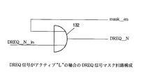
図2及び図3は上記DREQ信号マスク回路121,122の構成を示す回路図であり、図2はDREQ信号がアクティブ“H”の場合の回路構成を、図3はDREQ信号がアクティブ“L”(“L”レベルでアクティブな信号)の場合の回路構成をそれぞれ示す。
【0029】
図2において、DREQ信号がアクティブ“H”の場合のDREQ信号マスク回路121,122は、ANDゲート131により構成される。外部リクエストデバイス内部のDREQ信号をDREQ_P_in(アクティブ“H”の場合)とし、マスクを制御するマスク信号をmask_enとする。
【0030】
ANDゲート131は、マスク信号mask_enの反転信号とDREQ_P_in信号のAND論理をとりDREQ_Pを出力する。この場合、mask_en=“H”のときにDREQ_P_in信号がマスクされて、出力としてDREQ_Pが出力される。
【0031】
同様に、図3において、DREQ信号がアクティブ“L”の場合のDREQ信号マスク回路121,122は、ORゲート132により構成される。
【0032】
ORゲート132は、マスク信号mask_enとDREQ_N_in信号のOR論理をとりDREQ_Nを出力する。この場合、mask_en=“H”のときにDREQ_N_in信号がマスクされて、出力としてDREQ_Nが出力される。
【0033】
以下、上述のように構成されたDMA転送装置の動作を説明する。
【0034】
ここでは、mask_en0によりCH0のDREQ信号マスク回路121がイネーブルになり、mask_en1によりCH1のDREQ信号マスク回路122がイネーブルになる場合を説明する。
【0035】
図4は上記DMA転送装置のDMA転送動作を示すタイミングチャートであり、時間T(例えば、500ns)で1回のDMA転送が行われる。図中、CH0,CH1は、DMAC110の2つのDMAチャンネルを示す。
【0036】
図4に示すように、T1の区間でCH0/CH1の各々のDREGが同時に発生したとする。
【0037】
T2の区間においては、CH0のDREQ0信号は、mask_en0信号によってマスクされているため、CH1のDMA転送が行われている。そのとき、mask_en1信号はディセーブルの状態(“L”)である。
【0038】
次に、T3の区間においては、両方のDMAチャネルがマスクされているため、DMA転送が行われない。この区間では、CPU100がバスを占有し、プログラムに応じた処理を行っている。
【0039】
次に、T4の区間においては、mask_en1がイネーブルの状態(“H”)になっているため、CH1のDREQ1信号がマスクされ、DREQ1が出力されないため、DMAシーケンスが行われない。この区間では、CH0のDMA転送が行われる。
【0040】
次に、T5の区間においては、T3の区間と同様に、CPU100の処理が行われる。よって、ここでもCPU100の処理は停止しない。
【0041】
このように、mask_en0,mask_en1を利用して、DREQ信号をマスクしてDREQ0/DREQ1信号の発生周期を変えている。
【0042】
また、mask_en0/mask_en1は、CPU100が制御しているが、このような周期的なイネーブル信号は、CPU100の内蔵のタイマを使用して実現することが可能である。例えば、500nsの割り込み処理で、mask_en0/mask_en1を交互にイネーブルにするように設定すれば、各CHのDMAは、2μsに1回DREQが発生する。さらに、設定間隔を短くする場合には、CPU100から設定するのではなく、外部リクエストデバイスの内部に周期的にイネーブルを制御するタイマを内蔵することによって実現できる。
【0043】
以上説明したように、第1の実施形態に係るDMA転送装置は、CPU100、DMAC110、外部リクエストデバイス111、外部リクエストデバイス112及び外部メモリ113から構成され、外部リクエストデバイス111,112は、DREQ信号をマスクするDREQ信号マスク回路121,122を備え、DREQ信号マスク回路121,122がDREQ0/DREQ1信号をマスクしてDMA転送によるバス占有状態を制御するように構成したので、CPU100からのmask_en0/mask_en1信号(アクティブ“H”)により、DREQ信号マスク回路121,122が、DREQ0/DREQ1信号をマスクすることで、周期的にDREQ信号を発生させることにより、DMAによるシステバス占有率を制御することができる。その結果、DMAにバスを占有されてCPUの処理ができなくなることを避けることができ、システムのDMACの介在による破綻を防止するという効果がある。
【0044】
また、DMAC側の構成には一切変更がないため、既存のCPUシステムの変更なしにシステム全体のスループットの向上及び信頼性の向上を図ることができる。また、ゲート回路という簡単な部品の追加で実現できるので、低コストで実施できる。
【0045】
なお、本実施形態では、外部リクエストデバイス111,112の内部に、DREQ0/DREQ1信号をマスクするDREQ信号マスク回路121,122を設けるようにしているが、これらマスク回路121,122は外部リクエストデバイス側に設置されていればよく、必ずしも外部リクエストデバイスの内部に設置する構成でなくてもよい。
第2の実施形態
図5は本発明の第2の実施形態に係るDMA転送装置の構成を示すブロック図である。本実施形態は、DMACを使用して、外部メモリデバイスと外部リクエストデバイスとの間でDMA転送を行うシステムに適用した例である。本実施形態に係るDMA転送装置の説明にあたり前記図1と同一構成部分には同一符号を付している。
【0046】
図5において、DMA転送装置は、CPU100、DMAC200、外部リクエストデバイス240、外部リクエストデバイス241、及び外部メモリ113から構成される。
【0047】
DMAC200は、2つのDMAチャンネルを搭載しており、それらをCH0,CH1とする。また、CH0とCH1はそれぞれ、外部リクエストデバイス240、外部リクエストデバイス241に接続されている。
【0048】
DMAC200は、各チャンネル毎に設置され、CPU100からのマスク信号mask_en0,mask_en1により制御されるDREQ信号マスク回路210,220と、DREQ信号マスク回路210,220のBREQ0信号,BREQ1信号を調停する調停回路230とを備える。
【0049】
マスク信号mask_en0,mask_en1は、CH0とCH1のDREQ信号マスク回路210,220のイネーブル/ディセーブルの切替えをする信号であり、両信号ともアクティブ“H”である。
【0050】
なお、前記第1の実施形態のmask_en信号は、マスク信号そのものを意味するが、本実施形態を含む後述する各実施形態で記載されるmask_en信号はマスク回路を動作させるか否かを制御するための信号を意味する。したがって、必ずマスク回路を動作させる場合は、mask_en信号を省略することができる。
【0051】
CPU100は、このマスク信号mask_en0,mask_en1をDREQ信号マスク回路210,220に出力してDREQ信号マスク回路210,220を制御する。また、CPU100は、DREQ信号マスク回路210,220に対してタイマカウント値を設定することが可能であり、CPU100が設定するタイマカウント値によって、生成されるマスク信号の長さが変わる。
【0052】
外部リクエストデバイス240がDMAC200に出力するDREQ信号をDREQ0、外部リクエストデバイス241がDMAC200に出力するDREQ信号をDREQ1とし、DMAC200から外部リクエストデバイス240,241に返すDREQ0とDREQ1に対するDACK信号をそれぞれDACK0,DACK1とする。
【0053】
また、DMAC200からCPU100にBREQN信号(バス開放リクエスト信号:CPUに対して、バス権の開放を要求する信号/アクティブ“L”)が出力され、CPU100からDMAC200に対してBACKN信号(バス・アクノリッジ信号:外部DMACに対して、バス権の開放を許可していることを示す信号/アクティブ“L”)が出力される。
【0054】
ここで、DMAの転送方向は、外部リクエストデバイス→外部メモリ方向と、外部メモリ→外部リクエストデバイス方向の2通りあり、この転送方向は、CPU100がDMAC200に対して設定可能なものとする。
【0055】
図6は上記DREQ信号マスク回路210,220の構成を示すブロック図である。各チャンネルのDREQ信号マスク回路210,220は、同一構成をとるため、DREQ信号マスク回路210を代表して説明する。
【0056】
図6において、DREQ信号マスク回路210は、サンプリングクロックの立ち上がりエッジでカウント(デクリメント)するカウンタ回路211、カウントデータを所定値“0”と比較し、“0”とカウントデータが一致したときサンプリングクロックの周期分のパルス、すなわちカウンタTC(Terminal Count:最終カウントを意味する)信号を出力する比較器212、及びマスク回路213から構成される。
【0057】
カウンタ回路211には、データバスからカウントするための初期値と、カウントするためのサンプリングクロックが入力される。また、比較器212には、カウンタ回路211がカウントしたデータである現在のカウント値が入力され、比較器212からはカウンタTC信号が出力される。
【0058】
上記カウンタTC信号は、入力されてくるカウントデータ値が“0”になった区間で1サンプリングクロック分の幅で“H”のパルスになる信号であり、カウントが終了したことを示す。
【0059】
また、マスク回路213には、比較器212から出力されるカウンタTC信号が入力されるとともに、DREQ信号及びDACK信号が入力され、BREQ信号が出力される。
【0060】
図7は図6のマスク回路213の内部の詳細な構成を示す図である。
【0061】
図7において、マスク回路213は、カウンタTC信号を基にDACK信号が入力された時点で内部で生成されたマスク信号がイネーブルになるマスク信号を出力するマスク信号発生回路214、及び発生したマスク信号とDREQ信号のOR論理をとるORゲート215から構成される。
【0062】
以下、上述のように構成されたDMA転送装置の動作を説明する。
【0063】
図8はDMA転送装置の動作を説明するためのタイミングチャートである。なお、図中、番号(1)〜(5)は動作タイミングまたは動作の区間を説明するための符号である。
【0064】
2チャンネルCH0,CH1のうち、まずCH0のDREQ0信号マスク回路210を例にして説明する。
【0065】
図8のタイミングチャートにおいて、DREQ0信号は、DACK0信号がディセーブル(“L”)になってから、一定時間経過後にイネーブル(“H”)になるものとする。
【0066】
図8の(1)のタイミングでCPU100はDREQ0信号マスク回路210に対して、タイマカウント値をライトする。本動作の場合は、“5”をライトするものとする。
【0067】
次に、図8の(1)−1のタイミングでCPU100は、mask_en0を“H”にする。ここまでのCPU100の動作で、DREQ0信号マスク回路210は動作可能状態になる。
【0068】
次に、外部リクエストデバイス240から出力されるDREQ0信号がタイマに入力される。このとき、DREQ0信号マスク回路210は動作することなしに、DMAC200はDREQ0の入力のタイミングでBREQN信号をCPU100に対して出力する。
【0069】
BREQN信号を受け取ったCPU100は、ある決まったタイミング(CPUの仕様によって異なる)で、BACKN信号を出力する(図8の(2)−1の区間参照)。この区間は、DMAC200がバスを占有する区間であり、この区間ではCPU100はバス権を開放している状態になる。
【0070】
図8の(2)−1区間でDMAC200は、BACKN信号からDACK0信号を生成し、外部リクエストデバイス240に出力する。この時、DACK0信号の立ち下がりのタイミング(図8の(3)−1参照)で、マスク信号を“H”にする。その後、図8の(5)−1のタイミングでDREQ0信号は、マスク信号でマスクされる。
【0071】
ここで、図6及び図7を参照してDREQ信号マスク回路210,220のマスク動作について説明する。
【0072】
図6において、CPU100がカウンタ回路211に対してカウントの初期値(本実施形態では、“5h”)をセットする。このとき、DACK信号が入力されて初めてカウントが行われる。
【0073】
サンプリングクロックの立ち上がりエッジでカウント(デクリメント)が行われ、比較器212では、このカウントデータを所定値“0”と比較する。“0”とカウントデータが一致した場合は、サンプリングクロックの周期の分だけカウンタTC信号が出力される。
【0074】
一方、マスク回路213では、DACK信号が入力された時点で、内部のマスク信号発生回路214(図7)のマスク信号がイネーブル(アクティブ“H”)となり、ORゲート215でこのマスク信号とDREQ信号とのOR論理がとられ、BREQ信号として出力される。マスク信号がディセーブルになるためには、カウンタTC信号を使用し、マスク信号をディセーブルにする。このマスク信号は、マスク信号発生回路214で生成される信号で、DACK信号により“H”となり、カウンタTC信号で“L”となる信号である。
【0075】
図8のタイミングチャートの説明に戻る。
【0076】
入力にDREQ0信号と上記マスク信号から生成された出力を使用してBREQN信号を作成する。
【0077】
図8の(3)−1地点からサンプルクロックに同期して、DREQ信号マスク回路210のカウンタ回路211のカウンタがデクリメントされる。カウンタ値が“0”になった時点で、カウンタTC信号が発生する(アクティブ“H”)。
【0078】
このカウンタTC信号の立ち下がりを利用してマスク信号が“L”となり、マスクがディセーブルになる(図8の(4)−1参照)。マスク信号が“L”になった時点でマスク回路213のマスク信号が“L”になるので、DREQ0信号がそのままゲートを抜けて出力となる。この出力信号を利用して、BREQN信号が出力される(タイミングは図8の(4)−1参照)。
【0079】
ここで、図8の(5)−1〜(2)−2のBACKN信号の立ち下がりエッジまでの区間においては、BREQNが出力されないため、バス権はCPU100にあることになる。
【0080】
図8の(4)−1以降の動作シーケンスに関しては上記説明と同様である。
【0081】
図8に示すように、区間(2)−1、(2)−2、(2)−3はDMAC200がバス権を所有している区間であり、それ以外の区間はCPU100がバス権を所有している区間である。
【0082】
上記では、外部リクエストデバイス240に関しての動作の説明をしたが、外部リクエストデバイス241に関しても、同じ動作である。
【0083】
次に、CH0とCH1のDREQ0/DREQ1信号の調停に関して説明する。
【0084】
図9はDMA転送装置のDMAC200の調停動作を説明するためのタイミングチャートである。図中、○印はCH0のDMAシーケンスの開始を、●印はCH0のDMAシーケンスの開始を指し、番号(1)〜(2)は動作タイミングを説明するための符号である。また、DREQ信号監視CHは調停回路230の内部にある。
【0085】
DMAC200内部でのDREQ0/DREQ1信号の調停は、調停回路230によって、CH0→CH1→CH0→…の順(ラウンドロビン式)にDREQが入力されたかどうかを監視している。
【0086】
ここではT1区間の始まりにDREQ0、DREQ1が入力された場合を例にとり説明する。
【0087】
まず、図9の(1)の箇所で、DREQ監視がCH0を監視しているときに同時にDREQ0/DREQ1が入力されたことから、DREQ0が優先される。DREQ0を受けたBREQN信号は“L”となる(図9の○の部分参照)。
【0088】
次に、T3の区間((2)の箇所参照)でCH0のDMAシーケンスが終了した時点で、DREQ信号監視CHがCH1を示していて、しかも、DREQ1信号がイネーブルであるために、T4の区間でDREQ1を受けたBREQN信号が“L”となる(図9の●部分参照)。CH1のDMAシーケンスはT5区間で終了する。
【0089】
T6〜T8区間では、DREQ信号監視CHが1周期毎に、CH0/CH1のDREQ0/DREQ1を監視し、DREQ信号が入力されるのを待っている状態である。このとき、マスク信号CH0とマスク信号CH1が動作しているために、T6でDREQ0が、T8でDREQ1がマスクされている。
【0090】
T9において、マスク信号CH1が“L”になるために、T10区間でBREQN信号がイネーブル(“L”)になり、CH1のDMAシーケンスが行われ、T11区間でそのシーケンスが終了する。
【0091】
また、T12区間においてマスク信号CH0が“L”になり、なおかつ、DREQ監視CHが“0”を示しているため、T13区間でDREQ0を受けたBREQN信号が“L”となり、CH0のDMAシーケンスが行われる。
【0092】
このように、DREQ監視CHによってDREQ信号を監視して、有効になったDREQ信号と監視CHが同じくなった場合にBREQN信号を“L”にしてDMAシーケンスをスタートさせている。
【0093】
以上説明したように、第2の実施形態に係るDMA転送装置は、DMAC200が、各チャンネル毎に設置され、CPU100からのマスク信号mask_en0,mask_en1により制御されるDREQ信号マスク回路210,220と、DREQ信号マスク回路210,220のBREQ0信号,BREQ1信号を調停する調停回路230とを備え、DREQ信号マスク回路210,220がDREQ0/DREQ1信号をマスクしてDMA転送によるバス占有状態を制御するように構成したので、DMAC側(内部)で外部リクエストデバイスのDREQ信号をマスクすることによって、周期的にDREQ信号を発生させることにより、DMAによるシステムのバス占有率を制御することができ、DMAにバスを占有され、CPUの処理ができなくなることを避けることができ、システムの破綻を防止できるという効果がある。
【0094】
さらに、本実施形態では、DREQ信号マスク回路210,220をDMAC200内部に搭載するようにしているので、外部リクエストデバイスを新規に追加した場合に、新規デバイス搭載の度に、上記マスク回路を追加することによるハードウェアの増加を防ぐことができるという効果がある。
【0095】
また、DMAC側(内部)に調停回路230によるDREQ監視CHを搭載することで、DMA転送チャンネルに優先順位を付与し、均等にDMAのチャネルを配分することが可能になるという効果がある。
【0096】
なお、本実施形態では、DMAC200の内部に、DREQ信号をマスクするDREQ信号マスク回路210,220を設けるようにしているが、これらマスク回路210,220はDMAC側に設置されていればよく、必ずしもDMACの内部に設置する構成でなくてもよい。
第3の実施形態
図10は本発明の第3の実施形態に係るDMA転送装置の構成を示すブロック図である。本実施形態に係るDMA転送装置の説明にあたり前記図5と同一構成部分には同一符号を付している。
【0097】
図10において、DMA転送装置は、CPU100、DMAC300、外部リクエストデバイス350、外部リクエストデバイス351、外部リクエストデバイス352及び外部メモリ113から構成され、DMAC300は、BREQN信号をマスクするカウンタ付きマスク回路310を備えて構成される。
【0098】
DMAC300は、3つのDMAチャンネルを搭載しており、それらをCH0,CH1,CH3とする。また、CH0,CH1,CH2はそれぞれ、外部リクエストデバイス351、外部リクエストデバイス352、外部リクエストデバイス353に接続されている。
【0099】
外部リクエストデバイス351のDMAチャンネルをCH1、外部リクエストデバイス352のDMAチャンネルをCH2、外部リクエストデバイス353のDMAチャンネルをCH3とする。
【0100】
図10の破線に示すように、CH0,CH1,CH2毎に、外部リクエストデバイス351、外部リクエストデバイス352、外部リクエストデバイス353からDMAC300にDMA要求信号DREQ1,DREQ2,DREQ3が出力され、また、DMAC300から外部リクエストデバイス351、外部リクエストデバイス352、外部リクエストデバイス353にDMA許可信号DACK1,DACK2,DACK3が出力される。
【0101】
DMAC300は、CPU100に対してバス開放リクエスト信号BREQNを出力し、CPU100は、DMAC300に対してバス開放許可信号BACKNを出力する。
【0102】
また、CPU100からDMAC300に出力されるmask_en信号は、CPU100のポートから出力される信号であり、カウンタ付きマスク回路310のカウンタ回路をイネーブルにする信号(アクティブ“H”)である。
【0103】
図11は上記カウンタ付きマスク回路310の構成を示すブロック図である。
【0104】
図11において、サンプリングクロックの立ち上がりエッジでカウント(デクリメント)するカウンタ回路311と、カウントデータを所定値“0”と比較し、“0”とカウントデータが一致したときサンプリングクロックの周期分のパルス、すなわちカウンタTC信号を出力する比較器312と、DMAC300内部で作成したBREQ信号とmask_enマスク信号とのOR(論理和)を作成して、BREQN信号を作成するマスク回路313とから構成される。
【0105】
カウンタ回路311には、データバス、サンプルクロック、BACKN信号が入力され、現在のカウント値が出力される。
【0106】
比較器312には、カウンタ回路311から出力された現在のカウント値のデータが入力され、カウンタTC信号が出力される。
【0107】
マスク回路313には、DMAC300内部でDREQ信号から作成したBREQ信号、CPU100からのBACKN信号、mask_en信号、比較器312からカウンタTC信号が入力され、BREQN信号を出力する。
【0108】
図12は図11のマスク回路313の内部の詳細な構成を示す図である。
【0109】
図12において、マスク回路313は、カウンタTC信号を基にBACKN信号が入力された時点で内部で生成されたマスク信号がイネーブルになるマスク信号を出力するマスク信号発生回路314、及び発生したマスク信号とBREQ信号のOR論理をとるORゲート315から構成される。
【0110】
図13は上記DMA要求信号DREQ1,DREQ2,DREQ3からBREQN信号発生までの構成を示す図である。
【0111】
図13において、316は、外部リクエストデバイス351、外部リクエストデバイス352、外部リクエストデバイス353からのDREQ1,DREQ2,DREQ3信号を調停し、DMAC300内部で作成したBREQ信号を出力するDREQ信号調停回路である。
【0112】
DREQ信号調停回路316で作成されたBREQ信号は、マスク回路313(図11及び図12)に出力され、マスク回路313はBREQN信号を出力する。
【0113】
ここで、本実施形態のマスクカウンタ付きマスク回路310は、第2の実施形態のDREQ信号マスク回路210,220と同様に、ハード的なカウンタ(タイマ)を設けてマスク時間を決定する方法をとる。但し、第2の実施形態のようにハード的なカウンタ(タイマ)を設けてマスク時間を決定する方法も可能であるし、CPU自体のタイマ割り込みを利用して、CPUポートを利用してマスク時間を制御することも可能である。
【0114】
また、本実施形態では、マスク時間(外部リクエストデバイスの数に応じて選択する)になるように、マスクカウンタ付きマスク回路310内のカウンタ回路311のカウンタの値をセットするものであり、このカウンタに対して、所定のマスク時間になるようにデータをセットする。これも、CPU自体のタイマ割り込みを使ってでも実現可能である。
【0115】
以下、上述のように構成されたDMA転送装置の動作を説明する。
【0116】
まず、カウンタ付きマスク回路310の動作について述べる。
【0117】
図11に示すように、CPU100はカウンタ回路311にカウントすべき初期値をセット(本実施形態の場合は“5h”をセット)する。次に、BACKN信号が入力されると、サンプルクロックの立ち上がりエッジでカウント(デクリメント)が行われる。次に、比較器312により現在のカウント値を“0”と比較し、一致するとサンプルクロックの1周期分のパルスを出力する。
【0118】
一方、マスク回路313においては、図12に示すようにBACKN信号により内部のマスク信号がイネーブル(アクティブ“H”)となり、DMAC300内部でDREQから作成したBREQ信号と内部のマスク信号とのORゲート315の出力をBREQNとして出力する。ここで、内部のマスク信号は、BACKN信号にてイネーブル(アクティブ“H”)となり、カウンタTC信号にてディセーブル(アクティブ“L”)となる信号である。
【0119】
また、図10に示すように、mask_en信号はCPU100からDMAC300に入力される信号であり、CPU100のポートで制御される。このmask_en信号は、マスクカウンタ付きマスク回路310全体をイネーブルにするかディセーブルにするかを制御する信号であり、マスクカウンタ付きマスク回路310を使用しないでBREQを出力する場合は、CPU100はディセーブル(“L”)になるように制御する。
【0120】
図14はDMA転送装置の動作を説明するためのタイミングチャートである。
なお、図中、番号(1)〜(4)は動作タイミングまたは動作の区間を説明するための符号である。
【0121】
図14のタイミングチャートにおいて、DREQ1、DREQ2、DREQ3信号が図14の(2)のタイミングで同時にイネーブルになるものとする。各CH(CH1、CH2、CH3)のDMA要求の優先度は、CH1→CH2→CH3→CH1というようなラウンドロビン方式である。
【0122】
カウンタ付きマスク回路310のカウンタ値を“5”に設定した場合を例にする。
【0123】
図14の(1)のタイミングでカウント値“5”がセットされる。
【0124】
次に、図14の(2)のタイミングで、3つのDREQ(DREQ1、DREQ2、DREQ3)が同時にイネーブルになる。ここで、図14の(2)−1の区間はCH1のDMAが実行されている区間である。
【0125】
次に、図14の(3)−1のタイミング(BACKN信号の立ち上がり)でマスク信号イネーブルになり、BREQ信号がマスクされる。カウントの開始も、(3)−1の地点つまり、BACKN信号が“H”になったタイミングで開始される。BREQ信号のマスク回路は、前記図11のマスク回路313であり、DMAC300内部のBREQ信号がこのマスク回路313のマスク信号にてマスクされる。
【0126】
次に、図14の(4)−1のタイミングでカウンタ値が“0”となり、マスク信号が“L”(ディセーブル)になり、マスクが解除され、BREQN信号がDMAC300外部に出力される。図14の(2)−2の区間は、CH2のDMA転送が行われる。
【0127】
次に、図14の(3)−2のタイミング(BACKN信号の立ち上がり)でマスク信号がイネーブルになりBREQN信号がマスクされる。このマスク動作は、前記図11に示したマスク回路313により行われる。
【0128】
次に、図14の(4)−2のタイミングでカウンタが“0”となり、マスク信号が“L”(ディセーブル)になり、マスクが解除され、BREQN信号がDMAC300外部に出力される。
【0129】
このようにして、BREQN信号をマスクしてBREQNが発生する周期を調整している。
【0130】
以上説明したように、第3の実施形態に係るDMA転送装置は、DMAC300は、BREQN信号をマスクするカウンタ付きマスク回路310を備え、カウンタ付きマスク回路310がBREQN信号をマスクしてDMA転送によるバス占有状態を制御するように構成したので、第1及び第2の実施形態と同様の効果を得ることができる。
【0131】
特に、本実施形態によれば、第2の実施形態のように外部リクエストデバイスから出力されるDREQ信号をマスクするのではなく、DMAC300内部で、BREQN信号をマスクしている。このようにすると、第2の実施形態のように、各CHごとにマスク回路を付加するよりも、マスク回路を1個にすることができ、第2の実施形態の場合よりもハードウェアを小さくできる効果がある。
【0132】
また、BREQN信号をマスクするので、複数の外部リクエストデバイスからのDREQ信号が頻繁に重なってきた場合でも、BREQN信号を周期的に出力するように制御することが可能になり、DMAC300によるバス占有率を一定にできる効果がある。
第4の実施形態
図15は本発明の第4の実施形態に係るDMA転送装置の構成を示すブロック図である。本実施形態に係るDMA転送装置の説明にあたり前記図5と同一構成部分には同一符号を付している。
【0133】
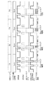
図15において、DMA転送装置は、CPU100、DMAC400、複数の外部リクエストデバイス(451,452,453,…,N−1,N)、及び外部メモリ113から構成される。
【0134】
DMAC400は、複数のDMAチャンネルを搭載しており、それらをCH1,CH2,CH3,…,CHN−1,CHNとする。また、CH1,CH2,CH3,…,CHN−1,CHNはそれぞれ、対応する外部リクエストデバイス(451,452,453,…,N−1,N)に接続されている。
【0135】
DMAC400は、CH1,CH2,CH3,…,CHN−1,CHNに対応して設置された複数のDREQ信号マスク回路410,…と、DREQ信号マスク回路410,…のBREQ信号を調停する調停回路230とを備える。
【0136】
外部リクエストデバイス451、外部リクエストデバイス452、外部リクエストデバイス453が出力するDREQ信号をそれぞれ、DREQ1、DREQ2、DREQ3とし、そのリクエスト信号に対するDACK信号をそれぞれ、DACK1、DACK2、DACK3とする。このとき、外部リクエストデバイス(N−1),外部リクエストデバイス(N)は、複数個外部リクエストデバイスがあるという意味で、DMAC400が対応可能な外部リクエストデバイスの数を示している。外部メモリ113は、DMAシステムのメモリであり、DMAシステムのソースデバイスにもなり、ディスティネーションデバイスにもなる。
【0137】
DMAC400内部には、マスクカウンタ及びマスク回路を内蔵したマスクカウンタ付きマスク回路(DREQ信号マスク回路)が各チャンネル毎に搭載されている。このマスク回路は、前記図2及び図3と同様な回路構成であり、マスクカウンタに対しては、CPU100がマスク時間に見合ったカウンタ値を設定する。
【0138】
DMAC400の内部のDREQ信号の調停回路230は、各チャンネルから出力されたDREQ信号を調停し、BREQN信号をCPU100に対して出力する。調停方法は、第2の実施形態と同様であり、DREQ信号の入力順番とDREQ信号監視CH(前記図9の動作説明参照)によりどのDMAシーケンスを行うか決定する。
【0139】
また、DMAC400からCPU100にBREQN信号(バス開放リクエスト信号:CPUに対して、バス権の開放を要求する信号/アクティブ“L”)が出力され、CPU100からDMAC400に対してBACKN信号(バス開放許可信号:外部DMACに対して、バス権の開放を許可していることを示す信号/アクティブ“L”)が出力される。
【0140】
以下、上述のように構成されたDMA転送装置の動作を説明する。
【0141】
図16はDMA転送装置の動作を説明するためのタイミングチャートである。
なお、図中、番号(1)〜(12)は動作タイミングまたは動作の区間を説明するための符号である。
【0142】
外部リクエストデバイス451、外部リクエストデバイス452、外部リクエストデバイス453からそれぞれDREQ1、DREQ2、DREQ3信号が任意のタイミングで同時(図16の(1)、(7)の地点)に出力された場合の動作について説明する。
【0143】
CPU100は、DMAコントローラ400内部のマスクタイマー(Ch1〜ChN)に対してマスク時間を設定する。設定値は図17に示す値である。本実施形態の場合、外部リクエストデバイスの個数が3個なので、図17に示す表からマスク時間=2μsに設定する。
【0144】
DMAC400は、任意のタイミングにおいて、1つのチャネルのDMAのみを有効にするため、チャンネルが有効になる順番をCh1,Ch2,…,ChNという順序で有効にする。
【0145】
図16のタイミングチャートにおいて、(1)、(7)地点でDREQ1を受けてBREQNが“L”となり、DMAシーケンスが開始される。このDMAシーケンスが終了したあと、(2)、(8)地点でMASK1信号がイネーブルになる。マスク時間の設定が2μsであるため、2μs分マスクされる。
【0146】
次に、図16の(3)、(9)のタイミングでDREQ2を受けて、BREQNが“L”となり、DMAシーケンスが開始される。図16の(4)、(10)のタイミングでこのDMAシーケンスが終了するが、このタイミングでマスクが開始される。
ここでも、マスク時間が2μs設定であるために、マスクは2μs分行われる。
【0147】
同様に、図16の(5)、(11)地点のタイミングでDREQ3を受けて、DMAシーケンスが開始されて、(6)、(12)地点でDMAシーケンスが終了し、マスクが開始される。この一連の流れにおいて、(6)の地点と(13)の地点の間に、DMAが行われていない区間が存在するが、この区間では、CPU100は、そのシステムのプログラムに準じた処理を行うことができる。この区間は、DREQのマスクがなければ存在しない区間である。この区間はDREQ1、DREQ2、DREQ3の発生周期と、外部リクエストデバイスを搭載する個数によって、決まってくる。
【0148】
以上説明したように、第4の実施形態に係るDMA転送装置は、DMAC400側(内部)に、CH1,CH2,CH3,…,CHN−1,CHNに対応して設置された複数のDREQ信号マスク回路410,…と、DREQ信号マスク回路410,…のBREQ信号を調停する調停回路230とを設け、各チャネル毎に配置された複数のDREQ信号マスク回路410,…が、CPU100により同時動作する外部リクエストデバイスの数に応じてマスク時間を制御するように構成したので、各DMAチャンネルのDMA転送の機会を時間的に均等に与えることが可能になりDMAチャンネルの時間的調停が可能になる。
【0149】
すなわち、複数の動作可能な外部リクエストデバイスが同一のバス上に存在する場合に、システムとしては、DMAC400がバスを占有する時間は自ずと増加する。つまり、DMAC400によるバス占有率が増加する。本実施形態では、DREQ信号のマスク時間を外部リクエストデバイスの同時動作する個数により制御することで、平均的なDMACのバス占有率を制御することができ、外部リクエストデバイスが複数存在することによる、システムにおけるDMAC400のバス占有率の著しい増加を防止することができる効果がある。
【0150】
なお、本実施形態では、DMAC400のバス占有率制御方法として第2の実施形態の方法を使用した例を示したが、第1の実施形態の方法に示したように、動作可能な外部リクエストデバイス側で制御することも、また第3の実施形態の方法でDMAC400のBREQを制御することによっても実現可能である。
第5の実施形態
図18は本発明の第5の実施形態に係るDMA転送装置の構成を示すブロック図である。本実施形態に係るDMA転送装置の説明にあたり前記図15と同一構成部分には同一符号を付している。
【0151】
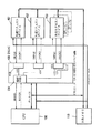
図18において、DMA転送装置は、CPU500、DMAC400、複数の外部リクエストデバイス(451,452,453,…,N−1,N)、及び外部メモリ113から構成される。
【0152】
CPU500のプログラムの中には、プログラムの処理タスクを管理するタスク管理機能510(管理手段)が搭載されている。
【0153】
DMAC400は、複数のDMAチャンネルを搭載しており、それらをCH1,CH2,CH3,…,CHN−1,CHNとする。また、CH1,CH2,CH3,…,CHN−1,CHNはそれぞれ、対応する外部リクエストデバイス(451,452,453,…,N−1,N)に接続されている。
【0154】
DMAC400は、CH1,CH2,CH3,…,CHN−1,CHNに対応して設置された複数のDREQ信号マスク回路410,…と、DREQ信号マスク回路410,…のBREQ信号を調停する調停回路230とを備える。
【0155】
外部リクエストデバイス451、外部リクエストデバイス452、外部リクエストデバイス453が出力するDREQ信号をそれぞれ、DREQ1、DREQ2、DREQ3とし、そのリクエスト信号に対するDACK信号をそれぞれ、DACK1、DACK2、DACK3とする。このとき、外部リクエストデバイス(N−1),外部リクエストデバイス(N)は、複数個外部リクエストデバイスがあるという意味で、DMAC400が対応可能な外部リクエストデバイスの数を示している。外部メモリ113は、DMAシステムのメモリであり、DMAシステムのソースデバイスにもなり、ディスティネーションデバイスにもなる。
【0156】
また、CPU500から出力されるmask_en1、mask_en2、mask_en3はそれぞれDREQ信号マスク回路410,…(DREQ信号マスク回路CH1、CH2、CH3)のマスクを有効にする信号である。制御は、CPU500自体がポート制御により行う。
【0157】
DMAC400の内部のDREQ信号の調停回路230は、各チャンネル(CH1/2/3…)のDREQ信号を調停し、BREQN信号をCPU500に出力する。調停方法は、第2の実施形態と同様である。
【0158】
また、DMAC400からCPU500にBREQN信号(バス開放リクエスト信号:アクティブ“L”)が出力され、また、このBREQN信号に応答して、CPU500は、DMAC400に対して、BACKN信号(バス開放許可信号:アクティブ“L”)を出力する。
【0159】
以下、上述のように構成されたDMA転送装置の動作を説明する。
【0160】
CPU500は、通常プログラムに則って処理をしているが、処理するタスクによっては、CPUに対する処理負荷が異なっている。CPU500の内部にあるタスク管理機能510は、現在何のタスクを処理しているかを常に監視し、その情報を保持する機能をもつものである。このタスク管理機能510はソフトウェアにより実現されている。
【0161】
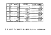
まず、プログラム上のタスク名T1〜T10とその処理負荷と対応するマスク時間の関係を図19の表に示す。
【0162】
図19に示すように、CPU500は、タスクをT1,T2,T3,…,T10,T1,…の順番で処理していくようなプログラムになっている。
【0163】
以下、DREQ1が連続して発生する時のDREQ1のイネーブル間隔が1μsである場合を例に挙げて説明する。
【0164】
図20はDMA転送装置の動作を説明するためのタイミングチャートである。
【0165】
まず、図20に示すように、タスクT1が処理されている最中は、マスク時間が1μsにセットされている(図19の表参照)。このときDREQ1信号がイネーブルされた場合、必ず1μs分DREQ1信号がDMAC400内部のマスクでマスクされて、DMA転送が行われる。この場合は、マスク設定時間が1μsであったが、DREQ1のイネーブル間隔が1μsであるために、マスクタイマが有効であってもまったく効果がない。
【0166】
次に、タスクT2が処理されている最中について説明する。このときは、マスク時間が2μsにセットされている(図19の表参照)。このとき、DREQ1信号がイネーブルされた場合、必ず2μs分DREQ1信号がDMAC400内部のDREQ信号マスク回路410でマスクされ、DMA転送が行われる。この場合は、DREQのイネーブル間隔が1μsであるのに対し、マスク設定時間が2μsであったため、マスクの効果が1μs出すことができたことになる。
【0167】
同様にして、タスクT3の場合は、マスクの効果が2μs、タスクT4の場合は3μsだけマスクの効果が出てくる。
【0168】
各チャンネル毎に上記動作を行う。また、各チャンネルの調停動作は第2の実施形態と同様である。
【0169】
以上説明したように、第5の実施形態に係るDMA転送装置は、CPU500が、プログラムの処理タスクを管理するタスク管理機能510を備え、CPUの処理負荷に応じてマスク時間を制御するように構成したので、以下のような効果を得ることができる。
【0170】
すなわち、CPU処理(タスク)が複雑であり、しかも、所定の時間内に処理を完了させなければならないタスクがシステム上に多くある場合、DMACから出力されるBREQ信号はそのCPU処理を時間的に非効率的にしてしまうことがある。このとき、本実施形態のように、タスクごとのDREQ信号のマスク動作を行うことで、CPU処理を所定の時間内に完了させることを遂行することができ、システム上のCPUの時間的処理能力の低下を防止することができる効果がある。
【0171】
なお、本実施形態では、DMACの動作を第2の実施形態の方法を制御したが、第1の実施形態に示したように、外部リクエストデバイス側で制御する方法でも、また第3の実施形態に示したように、DMAC内部のBREQ信号を制御する方法でも実現可能である。
第6の実施形態
図21は本発明の第6の実施形態に係るDMA転送装置の構成を示すブロック図である。本実施形態に係るDMA転送装置の説明にあたり前記図5と同一構成部分には同一符号を付している。
【0172】
図21において、DMA転送装置は、CPU100、DMAC600、外部リクエストデバイス650及び外部メモリ113から構成され、DMAC600は、DREQ信号マスク回路610(マスク手段)と、DREQ信号の発生周期を検出するDREQ周期検出回路620(DREQ周期検出手段)とを備えて構成される。
【0173】
外部リクエストデバイス650からDMAC600にDREQ信号が出力され、DMAC600から外部リクエストデバイス650にDACK信号が出力される。
【0174】
DMAC600からCPU100にBREQ信号が出力され、CPU100からDMAC600にBACK信号が出力される。
【0175】
また、外部メモリ113は、DMA転送のソースデバイス(または、ディスティネーションデバイス)になる。
【0176】
CPU100から出力されるmask_en信号は、DREQ信号マスク回路610を有効にする信号である。
【0177】
CPU100は、このマスク信号mask_enをDREQ信号マスク回路610に出力してDREQ信号マスク回路610を制御する。
【0178】
図22は上記DREQ周期検出回路620の回路構成を示す図である。
【0179】
図22において、DREQ周期検出回路620は、DREQ信号を入力してDREQ信号のエッジを論理的に検出するエッジ検出回路621、サンプリングクロックの立ち上がりエッジでカウント(デクリメント)するカウンタ622、及びカウントデータを格納するデータバッファ623から構成される。
【0180】
データバッファ623は、カウンタ623の結果をCPU100(図21)がリードできるようにデータを保持しておくバッファである。
【0181】
以下、上述のように構成されたDMA転送装置の動作を説明する。
【0182】
図23はDREQ周期検出回路620の動作を示すタイミングチャートである。
【0183】
まず、外部リクエストデバイス650からDREQ信号がDMAC600に入力され、その入力信号が内部のDREQ周期検出回路620に入力される。
【0184】
DREQ周期検出回路620の内部回路においては、図23のタイミングチャートに示すように、エッジ検出部621がDREQ信号の立ち上がりエッジを検出し、検出したパルスをトリガとして、カウンタ622がカウントを開始する。
このカウントは次のDREQ信号のエッジまでカウントする。
【0185】
カウンタ622によりカウントされたカウントデータは、データバッファ623に転送され、カウント終了後はデータバッファ623はそのデータを保持している。
【0186】
図24はDMA転送装置の動作を説明するためのタイミングチャートである。
【0187】
CPU100は、データバッファ623のカウントデータを任意のタイミングで読み出し、そのデータに従ってCPUのポートにより、mask_en信号のイネーブル/ディセーブルの操作を行う。すなわち、CPU100は、読み出したカウントデータが小さければmask_en信号をイネーブルにしている時間を長くする。
【0188】
図24に示すように、mask_en信号がイネーブルの場合、DREQ信号は一定期間(区間)マスクされ、マスク解除後、mask_en信号がディセーブルとなりBREQ信号となってCPU100に出力される。
【0189】
BREQ信号を受け付けたCPU100は、バス権を開放したことを知らせるためにBACK信号を出力する。
【0190】
図24に示すように、mask_en信号がディセーブルの区間は、BREQ信号の発生間隔が短くなっているが、mask_en信号がイネーブルの区間はBREQの発生間隔がディセーブルの区間に比べて長くなっているのがわかる。
この区間(マスク効果が出ている区間)では、CPU100がプログラムに従って処理している区間である。
【0191】
以上説明したように、第6の実施形態に係るDMA転送装置は、DMAC600が、DREQ信号マスク回路610と、DREQ信号の発生周期を検出するDREQ周期検出回路620とを備え、DREQ周期検出回路620が入力されるDREQ信号の発生周期を検出し、そのカウンタデータ値を利用してDREQ信号をマスクするように構成したので、DMAの周期(間隔)を広げることができ、しかも、DMAC600による、システムにおけるバス占有率を低減するという効果がある。
【0192】
また、この方法を使用すれば、DMA転送のスピードをCPU100によって制御することが可能になるため、DREQ信号発生周期が変動するI/O装置(外部リクエストデバイス)がバス上に存在する場合、同じ周期でBREQ信号を発生させ、バス占有率を低減させる効果がある。
【0193】
なお、本実施形態においては、DMACの動作を第2の実施形態の方法で制御したが、第1の実施形態の方法に示したように、動作可能な外部リクエストデバイス側で制御することも、また第3の実施形態の方法に示したようにDMAC内部のBREQを制御する方法でも実現可能である。
第7の実施形態
図25は本発明の第7の実施形態に係るDMA転送装置の構成を示すブロック図である。本実施形態に係るDMA転送装置の説明にあたり前記図21と同一構成部分には同一符号を付している。
【0194】
図25において、DMA転送装置は、CPU100、DMAC700、外部リクエストデバイス751、外部リクエストデバイス752及び外部メモリ113から構成され、DMAC700は、BREQN信号マスク回路720(マスク手段)と、動作を許可する複数の外部リクエストデバイスのDREQ信号に伴い発生するBREQN信号の発生周期を検出するBREQN周期検出回路720(BREQN周期検出手段)とを備えて構成される。
【0195】
DMAC700は、複数の(2つの)DMAチャンネルを搭載しており、それらをCH1,CH2とする。また、CH1,CH2はそれぞれ、外部リクエストデバイス751、外部リクエストデバイス752に接続されている。
【0196】
外部リクエストデバイス751のDMAチャンネルをCH1、外部リクエストデバイス752のDMAチャンネルをCH2とする。
【0197】
図25の破線に示すように、CH1,CH2毎に、外部リクエストデバイス751、外部リクエストデバイス752からDMAC700に対してDMA要求信号DREQ1,DREQ2(アクテイブ“H”)が出力され、また、DMAC700から外部リクエストデバイス751、外部リクエストデバイス752に対してDMA許可信号DACK1,DACK2が出力される。
【0198】
DMAC700は、CPU100に対してバス開放リクエスト信号BREQN(アクティブ“L”)を出力し、CPU100は、DMAC700に対してバス開放許可信号BACKN(アクティブ“L”)を出力する。
【0199】
また、CPU100からDMAC700に出力されるmask_en信号は、CPU100のポートから出力される信号であり、BREQNマスク回路720のカウンタ回路をイネーブルにする信号(アクティブ“H”)である。
【0200】
図26は上記BREQN信号周期検出回路720の回路構成を示す図である。
【0201】
図26において、BREQN信号周期検出回路720は、BREQN信号を入力してBREQN信号のエッジを論理的に検出するエッジ検出回路721、サンプリングクロックの立ち上がりエッジでカウント(デクリメント)するカウンタ722、及びカウントデータを格納するデータバッファ723から構成される。
【0202】
エッジ検出回路721からカウントパルスがカウンタに対して出力され、カウンタ722から、カウントデータがデータバッファ723に転送される。
【0203】
データバッファ723は、カウンタ723の結果をCPU100(図25)がリードできるようにデータを保持しておくバッファである。
【0204】
以下、上述のように構成されたDMA転送装置の動作を説明する。
【0205】
図27はBREQN信号周期検出回路720の動作を示すタイミングチャートであり、図28はDMA転送装置の動作を説明するためのタイミングチャートである。
【0206】
まず、CH1とCH2のDMA転送の優先度は、本実施形態の場合、CH1→CH2→CH1→CH2のようにラウンドするラウンドロビン型をとるものとする。同時にDREQ(要求信号)がDMAC700に入力された場合は、CH1優先とし、その他の場合は、時間的に先にDREQ(要求信号)が入ってきた方を優先とする。
【0207】
DREQ1とDREQ2が同時に図28の(1)の地点でアクティブになっている場合を例にする。このとき、DMAは、CH1のDMAが行われる。
【0208】
次に、図28の(2)の地点で、CH2のDMAが行われる。このとき、図28の(1)と(2)のBREQN信号の立ち下がりエッジで、図26に示すBREQN信号周期検出回路720が動作し、カウンタ722が動作する。そして、図27のタイミングチャートに示すように、カウントデータがデータバッファ723に転送される。
【0209】
また、図28の(3)の地点でCH1のDMAが実行されるが、このときも、BREQN信号周期検出回路720により図28の(2)と(3)のBREQNのエッジからエッジの間のカウントが行われる。この時のカウントデータも、データバッファ723に上書きされる。
【0210】
図28の(3)のDMA転送終了した時点でCPU100は、データバッファ723のデータをリードする。このリードした値で、DMAC700のBREQN信号の発生周期をCPU100が認識することができる。
【0211】
次に、図28の(4)−1の地点、つまりBACKN信号が“H”になった時点で、CPU100は、mask_en1信号を“H”にする。mask_en1を“H”にした時点で、BREQN信号は、マスクされていて、DREQ1、DREQ2が入力されても、BREQN信号は外部に出力されない(図28のマスク効果が出ている区間参照)。
【0212】
図28の(4)−2、(4)−3地点でも同様である。
【0213】
CPU100がmask_en1を“H”にする時間は、先にリードしたBREQ信号の発生周期の値をもとに制御する。例えば、データバッファ723からリードした数値が極端に短かかった場合は、mask_en1を“H”にしている時間を長くして、DMAC100によるバス占有率を低下させ、逆に、データバッファ723からリードした数値が極端に長かった場合には、mask_en1信号を“H”にする時間を短めに制御することが可能である。
【0214】
このように、BREQの発生周期をCPU100が認識することで装置のDMAC700によるバス占有率をCPU100が制御することが可能である。
【0215】
以上説明したように、第7の実施形態に係るDMA転送装置は、DMAC700が、BREQN信号マスク回路720と、動作を許可する複数の外部リクエストデバイスのDREQ信号に伴い発生するBREQN信号の発生周期を検出するBREQN周期検出回路720とを備え、BREQN信号周期検出回路720は、BREQN信号を入力してBREQN信号のエッジを論理的に検出するエッジ検出回路721、サンプリングクロックの立ち上がりエッジでカウント(デクリメント)するカウンタ722、及びカウントデータを格納するデータバッファ723により構成したので、BREQN信号の発生周期(発生間隔)をBREQNの信号のエッジを使用してカウントし、カウントデータをデータバッファ723に保持しておくことで、CPU100が、DMAC700から入力されるBREQの発生周期を認識することできるようになり、CPU100によって、DMAC700によるバス占有率を制御することが可能になる。
【0216】
また、第6の実施形態のように、CH(チャンネル)ごとに、DREQの発生周期を検出するDREQ周期検出回路620を搭載すると、外部リクエストデバイスを多数搭載したときに、DREQ周期検出回路を構成するカウンタや、データバッファを新規にCHごとに追加する必要がある。本実施形態によれば、BREQN信号に対して、BREQN周期検出回路720を搭載しているために、外部リクエストデバイスが多数搭載されても、BREQN周期検出回路を構成するカウンタやデータバッファは1個のみで済むので、ハードウェアの規模を小さくできる効果がある。
【0217】
なお、本実施形態では、第3の実施形態の方法でDMACの動作を制御したが、制御の方法はCPUによる制御でも、マスク回路にハード的なタイマーを設けて、ハードでマスクすることも可能である。また、第1の実施形態の方法に示したように、動作可能な外部リクエストデバイス側で制御することも、第2の実施形態の方法に示したように、DMAC側で制御することも可能である。
第8の実施形態
図29は本発明の第8の実施形態に係るDMA転送装置の構成を示すブロック図である。本実施形態に係るDMA転送装置の説明にあたり前記図18及び図21と同一構成部分には同一符号を付している。
【0218】
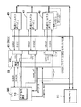
図29において、DMA転送装置は、CPU800(設定手段)、DMAC600、外部リクエストデバイス650及び外部メモリ113から構成され、DMAC600は、DREQ信号マスク回路610と、DREQ周期検出回路620とを備えて構成される。
【0219】
CPU800のプログラムの中には、プログラムの処理タスクを管理するタスク管理機能810(管理手段)が搭載されている。このタスク管理機能810はソフトウェアにより実現されている。
【0220】
DMAC600は、外部リクエストデバイス650からDREQ信号が入力され、マスクイネーブルの場合はDREQ信号をmask_en信号の区間分だけマスクしてBREQN信号をCPU800に対して出力する。CPU800がバス権を開放したときにBACKN信号がDMAC600に出力される。
【0221】
そのBACKN信号を受けてDMAC600は、外部リクエストデバイス650に対して、DACK信号を出力する。
【0222】
DREQ周期検出回路620は、第6の実施形態の図22と同じ回路構成である。
【0223】
以下、上述のように構成されたDMA転送装置の動作を説明する。
【0224】
まず、システム全体のバス負荷率を規定する。説明を簡単にするために、本実施形態ではシステム全体のバス負荷率を12%以下とする。また、外部リクエストデバイス650のDREQ信号発生間隔を5μsとし、1回(Word分)のDMA転送のバス占有率を10%とする。これによりDMAでバスを占有する時間=500nsとなる。
【0225】
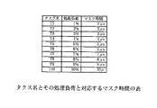
まず、プログラム上のタスク名T1〜T10とその処理負荷と対応するマスク時間及びDMACの負荷率の関係を図30の表に示す。
【0226】
図30に示すように、本実施形態は、タスクT1〜T10を使って処理するシステムであり、その中のT1,T3,T5,T7を図31に示すタイミングチャートのような順序でタスク処理していく場合を考える。
【0227】
図31はDMA転送装置の動作を説明するためのタイミングチャートである。
【0228】
まず、DREQ信号がタスクT1区間で入力される。この場合、図30の表から計算すると、合計のバス占有率が11%となり、本実施形態の占有率12%を超えることはない。そのためマスク回路を動作させる必要はないために、mask_en信号はディセーブルのままで、何ら問題がない。よってDREQ信号と同じ周期でBREQ信号が発生する。
【0229】
次に、タスクT3区間でDREQ信号が発生した場合、図30の表とDMAのバス占有率から計算すると13%となってしまう。本実施形態のバスの占有率は12%以下であるため、問題が生じる。このようなことが起きないように、処理がタスクT3に入った場合にmask_en信号を図31に示すタイミングで出力するようにCPU800がコントロールする。このとき、DREQ信号はmask_en信号によりマスクされてBREQ信号としてCPU800に出力される。このBREQ信号によってCPU800はバス権を開放するためにBACK信号を出力する。このようなやり取りでDMA転送のシーケンスを実行する。
【0230】
次に、タスクT5区間にDREQ信号が入力された場合を説明する。
【0231】
この場合はタスクT3の場合と同様にバス占有率を計算すると15%になってしまう。これもまた、本実施形態のバス占有率12%以下を満たしていないので、この条件を満たすために、図30の表を使用してマスク時間を設定する。
【0232】
この表によればT5の場合は、mask_enがイネーブルの時間が2.14μs+5μsとなり、バス占有率が12%以下になる。この時のマスク時間を満たすようにCPU800がmask_enを制御する。
【0233】
同様に、タスクT7の場合も図30の表からマスク時間を設定して、本実施形態で設定したバス占有率12%以下になるようにmask_en時間を決め、このマスク時間を満たすようにCPU800がmask_enを制御する。
【0234】
以上説明したように、第8の実施形態に係るDMA転送装置は、CPU800が、プログラムの処理タスクを管理するタスク管理機能810を備え、CPUの処理負荷に応じて所定のシステムのバス負荷を保持して、マスク時間を制御するように構成したので、各タスクが動作しているときのバス占有率を予め計算しておき、その計算値からシステム全体のバス占有率の限界値を設定し、CPU処理が効果的でかつ、DMA周期もバス占有率の上限を超えないような値で行うことが可能になり、予め計算していたバス占有率の値まで、確実にバス占有率を低減する効果がある。
【0235】
なお、本実施形態は、第2の実施形態の方法でDMACを制御していたが、第1の実施形態の方法に示したように、動作可能な外部リクエストデバイス側で制御することも、第3の実施形態の方法でDMAC内部のBREQ信号を制御することによっても実現可能である。
【0236】
また、マスク時間はCPUによって制御することも、マスク回路にハード的なタイマを設けてCPUからタイマの時間をセットすることによって実現することも可能である。
【0237】
したがって、このような特長を有するDMA転送装置を、例えば、プリンタなどに代表されるような、PC(パーソナルコンピュータ)周辺機器において、PCからのデータ転送速度と周辺機器自身のデータ処理速度がお互いに高速処理が必要な場合で、しかもシステムの破綻を避けることが不可欠なシステムにおいて、データ転送とCPU処理を時間的に均等に処理したい場合に有効である。また、CPUを中心としたDMAによるデータ転送を含むすべてのシステムにおいて利用可能である。
【0238】
また、上記各実施形態では、外部リクエストデバイスまたはDMAC内にマスク回路等を設置するようにしているが、これは一例であり、外部に外付けするように設置してもよい。また、DMACは、専用のDMAコントローラでも汎用のDMAコントローラでもよく、特に、高速性が要求されるときにはカウンタ及びバッファ等の個別部品を用いて構成するものでもよい。
【0239】
さらに、上記DMA転送装置を構成するレジスタ、カウンタ、各種制御回路等の種類、数などは上述した実施形態に限られないことは言うまでもない。
【0240】
【発明の効果】
本発明に係るDMA転送装置では、外部リクエストデバイスまたはDMA制御部が、DREQ信号をマスクするマスク手段を備え、マスク手段によりDREQ信号をマスクしてDMA転送によるバス占有状態を制御するように構成したので、外部リクエストデバイスが複数存在する場合、または、DREQ信号の発生周期が短い外部リクエストデバイスが同一のバスに存在する場合、DMAによるバス占有率を低減でき、時間的にバスを有効に利用することができる。
【図面の簡単な説明】
【図1】本発明を適用した第1の実施形態に係るDMA転送装置の構成を示すブロック図である。
【図2】上記DMA転送装置のDREQ信号マスク回路の構成を示す回路図である。
【図3】上記DMA転送装置のDREQ信号マスク回路の構成を示す回路図である。
【図4】上記DMA転送装置のDMA転送動作を示すタイミングチャートである。
【図5】本発明を適用した第2の実施形態に係るDMA転送装置の構成を示すブロック図である。
【図6】上記DMA転送装置のDREQ信号マスク回路の構成を示すブロック図である。
【図7】上記DMA転送装置のマスク回路の内部の詳細な構成を示す図である。
【図8】上記DMA転送装置の動作を説明するためのタイミングチャートである。
【図9】上記DMA転送装置のDMACの調停動作を説明するためのタイミングチャートである。
【図10】本発明を適用した第3の実施形態に係るDMA転送装置の構成を示すブロック図である。
【図11】上記DMA転送装置のカウンタ付きマスク回路の構成を示すブロック図である。
【図12】上記DMA転送装置のマスク回路の内部の詳細な構成を示す図である。
【図13】上記DMA転送装置のDMA要求信号DREQ1,DREQ2,DREQ3からBREQN信号発生までの構成を示す図である。
【図14】上記DMA転送装置の動作を説明するためのタイミングチャートである。
【図15】本発明を適用した第4の実施形態に係るDMA転送装置の構成を示すブロック図である。
【図16】上記DMA転送装置の動作を説明するためのタイミングチャートである。
【図17】上記DMA転送装置のマスク時間を設定の表を示す図である。
【図18】本発明を適用した第5の実施形態に係るDMA転送装置の構成を示すブロック図である。
【図19】上記DMA転送装置のプログラム上のタスク名とその処理負荷と対応するマスク時間の関係の表を示す図である。
【図20】上記DMA転送装置の動作を説明するためのタイミングチャートである。
【図21】本発明を適用した第6の実施形態に係るDMA転送装置の構成を示すブロック図である。
【図22】上記DMA転送装置のDREQ周期検出回路の回路構成を示す図である。
【図23】上記DMA転送装置のDREQ周期検出回路の動作を示すタイミングチャートである。
【図24】上記DMA転送装置の動作を説明するためのタイミングチャートである。
【図25】本発明を適用した第7の実施形態に係るDMA転送装置の構成を示すブロック図である。
【図26】上記DMA転送装置のBREQN信号周期検出回路の回路構成を示す図である。
【図27】上記DMA転送装置のBREQN信号周期検出回路の動作を示すタイミングチャートである。
【図28】上記DMA転送装置の動作を説明するためのタイミングチャートである。
【図29】本発明を適用した第8の実施形態に係るDMA転送装置の構成を示すブロック図である。
【図30】上記DMA転送装置のプログラム上のタスク名とその処理負荷と対応するマスク時間の関係の表を示す図である。
【図31】上記DMA転送装置の動作を説明するためのタイミングチャートである。
【図32】従来のDMA転送装置の構成を示すブロック図である。
【図33】従来のDMACの調停のタイミングを概念的に示すタイミングチャートである。
【符号の説明】
100,500,800 CPU、110,200,300,400,600,700 DMAC(DMA制御部)、111,112,240,241,351,352,353,451,452,453,751,752 外部リクエストデバイス、113 外部メモリ、121,122,210,220,410,610 DREQ信号マスク回路(マスク手段)、131 ANDゲート、132 ORゲート、230 調停回路、211,311 カウンタ回路、212,312 比較器、213,313 マスク回路、214 マスク信号発生回路、215,315 ORゲート、310 カウンタ付きマスク回路(マスク手段)、316 DREQ信号調停回路、313 BREQ信号マスク回路、314 マスク信号生成回路、510,810 タスク管理機能(管理手段)、620 DREQ周期検出回路(DREQ周期検出手段)、621,721 エッジ検出回路、622,722 カウンタ、623,723 データバッファ、710 BREQN信号マスク回路(マスク手段)、720 BREQN周期検出回路(BREQN周期検出手段)[0001]
BACKGROUND OF THE INVENTION
The present invention relates to a DMA (Direct Memory Access) transfer apparatus, and more specifically, a DMA having a DMA control unit that performs DMA transfer control for directly transferring data between a memory and an external request device independently of the operation of a CPU. The present invention relates to a transfer device.
[0002]
[Prior art]
In the DMA transfer, data is directly transferred between peripheral devices such as a main memory and an I / O device (for example, an external request device) without using a CPU. This enables high-speed and large-capacity data transfer without CPU overhead. In general, the DMA transfer is controlled by a direct memory access controller (DMAC) managing the bus.
[0003]
Conventionally, in a system that performs DMA transfer between a DMAC and an external request device, the DMAC receives a DMA request (DREQ) signal output from the external request device so that data can be transferred between the memory device and the external request device. Control other devices.
[0004]
FIG. 32 is a block diagram showing the configuration of a conventional DMA transfer apparatus, taking as an example data transfer between a DMAC and an external request device.
[0005]
In FIG. 32, 1 is a CPU, 2 is a DMAC, 3 and 4 are a plurality of (two) external request devices (
[0006]
Request signals DREQ1 / DREQ2 are output from the
[0007]
Upon receiving the BREQ, the
[0008]
[Problems to be solved by the invention]
However, such a conventional DMA transfer apparatus requires arbitration of the DREQ signal when mounted in a plurality of external request device systems as described above. In addition, the bus occupation rate by the DMA increases depending on the number of external request devices and the DREQ signal generation cycle of the external request device, and there is a possibility that processing by a normal series of CPUs may be extremely prolonged. was there.
[0009]
Hereinafter, this defect will be described.
[0010]
FIG. 33 is a timing chart conceptually showing the timing of DMAC arbitration.
[0011]
In a DMAC having three channels, the time required for one DMA transfer of each CH is T. In the case of FIG. 33, the DMAC arbitrates the DMA of each channel, and uses the channel in a round robin system such as CH1 → CH2 → CH3 → CH1. However, when this method is used, the bus is occupied only for DMA transfer, and the time that the processor is processing using the bus may be extremely extended in time.
[0012]
In the present invention, when there are a plurality of external request devices, or when external request devices having a short DREQ signal generation period exist on the same bus, the bus occupancy rate by DMA is reduced and the bus is made effective in time. An object of the present invention is to provide a DMA transfer apparatus that can be used.
[0014]
[Means for Solving the Problems]
The DMA transfer apparatus according to the present inventionA CPU, an external memory, a plurality of external request devices each generating a data transfer request signal,Independent of CPU operation,OutsideMemory andThe plurality ofExternal request deviceBetweenDMA transferThecontrolDoDMA controllerA bus connecting the CPU, the external memory, the plurality of external request devices, and the DMA control unit;With
The DMA control unit,in frontRecordpluralExternal request deviceAny ofData transfer request signalTheWhen it occursIn, Request a bus release by outputting a bus release request signal to the CPU, and when a bus release permission signal is returned from the CPU,The data transfer request signal was generatedSend a data transfer request confirmation signal to the external request deviceTheThe aboveOutsideMemory andThe data transfer request signal was generatedExternal request deviceWithDMA transfer betweenThecontrolBefore andBus request signal by masking the data transfer request signal so as to control the bus occupation state by DMA transferGenerateA mask circuit and a counter for counting a mask time for masking the data transfer request signal.And provided for each of the plurality of external request devicesMask means;in frontThe mask circuit of the mask meansOne ofByGenerationBased on the received bus request signal,The means for controlling the DMA transfer to the CPUBus release request signalAdjust the output of theMediation means to mediate andHave
The CPU includes means for controlling the mask time according to the number of external request devices that can be operated simultaneously, and task management means for managing a processing load of a task processed by the CPU itself,
The task management means is monitored by the monitoring means for holding information on the mask time set for each task processed by the CPU, a monitoring means for monitoring a task currently processed by the CPU, and the monitoring means. Selection means for selecting the mask time from means for holding information on the mask time according to the task being set, and setting means for setting the selected mask time as a mask time used by the mask circuit. HaveIt is characterized by that.
[0021]
DETAILED DESCRIPTION OF THE INVENTION
First embodiment
FIG. 1 is a block diagram showing the configuration of the DMA transfer apparatus according to the first embodiment of the present invention. The present embodiment is applied to a system that performs DMA transfer between an external memory and an external request device.
[0022]
In FIG. 1, the DMA transfer apparatus includes a
[0023]
The DMAC 110 is equipped with two DMA channels, which are CH0 and CH1. Further, CH0 and CH1 are connected to the
[0024]
A DREQ signal mask circuit 121 (mask means) is installed inside the
[0025]
The mask signals mask_en0 and mask_en1 are signals for controlling enable / disable of the DREQ
[0026]
Also, a BREQ (bus opening request) signal is output from the
[0027]
The
[0028]
2 and 3 are circuit diagrams showing configurations of the DREQ
[0029]
In FIG. 2, the DREQ
[0030]
The AND
[0031]
Similarly, in FIG. 3, the DREQ
[0032]
The OR
[0033]
Hereinafter, the operation of the DMA transfer apparatus configured as described above will be described.
[0034]
Here, a case will be described in which the DREQ
[0035]
FIG. 4 is a timing chart showing the DMA transfer operation of the DMA transfer apparatus. One DMA transfer is performed at time T (for example, 500 ns). In the figure, CH0 and CH1 indicate two DMA channels of the
[0036]
As shown in FIG. 4, it is assumed that DREGs of CH0 / CH1 are generated at the same time in the interval of T1.
[0037]
In the period T2, the CH0 DREQ0 signal is masked by the mask_en0 signal, and therefore the CH1 DMA transfer is performed. At that time, the mask_en1 signal is in a disabled state (“L”).
[0038]
Next, in the period T3, since both DMA channels are masked, DMA transfer is not performed. In this section, the
[0039]
Next, in period T4, mask_en1 is enabled ("H"), so the DREQ1 signal of CH1 is masked and DREQ1 is not output, so no DMA sequence is performed. In this section, the DMA transfer of CH0 is performed.
[0040]
Next, in the T5 section, the processing of the
[0041]
In this way, mask_en0 and mask_en1 are used to mask the DREQ signal and change the generation period of the DREQ0 / DREQ1 signal.
[0042]
Further, mask_en0 / mask_en1 is controlled by the
[0043]
As described above, the DMA transfer apparatus according to the first embodiment includes the
[0044]
Further, since there is no change in the configuration on the DMAC side, it is possible to improve the throughput and reliability of the entire system without changing the existing CPU system. Moreover, since it can be realized by adding a simple part called a gate circuit, it can be implemented at low cost.
[0045]
In the present embodiment, the DREQ
Second embodiment
FIG. 5 is a block diagram showing a configuration of a DMA transfer apparatus according to the second embodiment of the present invention. The present embodiment is an example applied to a system that performs DMA transfer between an external memory device and an external request device using DMAC. In the description of the DMA transfer apparatus according to the present embodiment, the same components as those in FIG.
[0046]
In FIG. 5, the DMA transfer apparatus includes a
[0047]
The
[0048]
The
[0049]
The mask signals mask_en0 and mask_en1 are signals for switching enable / disable of the DREQ
[0050]
Note that the mask_en signal in the first embodiment means the mask signal itself, but the mask_en signal described in each embodiment to be described later including this embodiment controls whether or not to operate the mask circuit. Signal. Therefore, the mask_en signal can be omitted when the mask circuit is always operated.
[0051]
The
[0052]
The DREQ signal output from the
[0053]
Also, the BREQN signal (bus release request signal: signal requesting the release of the bus right / active “L” to the CPU) is output from the
[0054]
Here, there are two DMA transfer directions: external request device-> external memory direction and external memory-> external request device direction. This transfer direction can be set for the
[0055]
FIG. 6 is a block diagram showing the configuration of the DREQ
[0056]
In FIG. 6, a DREQ
[0057]
The
[0058]
The counter TC signal is a signal that becomes a pulse of “H” with a width corresponding to one sampling clock in the interval in which the input count data value becomes “0”, and indicates that the count is completed.
[0059]
The
[0060]
FIG. 7 is a diagram showing a detailed configuration inside the
[0061]
In FIG. 7, the
[0062]
Hereinafter, the operation of the DMA transfer apparatus configured as described above will be described.
[0063]
FIG. 8 is a timing chart for explaining the operation of the DMA transfer apparatus. In the figure, the numbers (1) to (5) are symbols for explaining the operation timing or the operation interval.
[0064]
Of the two channels CH0 and CH1, first, the CH0 DREQ0
[0065]
In the timing chart of FIG. 8, it is assumed that the DREQ0 signal is enabled (“H”) after a lapse of a certain time after the DACK0 signal is disabled (“L”).
[0066]
At timing (1) in FIG. 8, the
[0067]
Next, at the timing of (1) -1 in FIG. 8, the
[0068]
Next, the DREQ0 signal output from the
[0069]
The
[0070]
In section (2) -1 of FIG. 8, the
[0071]
Here, the mask operation of the DREQ
[0072]
In FIG. 6, the
[0073]
Counting (decrementing) is performed at the rising edge of the sampling clock, and the
[0074]
On the other hand, in the
[0075]
Returning to the description of the timing chart of FIG.
[0076]
A BREQN signal is created by using the DREQ0 signal as an input and the output generated from the mask signal.
[0077]
The counter of the
[0078]
Using the falling edge of the counter TC signal, the mask signal becomes “L” and the mask is disabled (see (4) -1 in FIG. 8). When the mask signal becomes “L”, the mask signal of the
[0079]
Here, since BREQN is not output in the interval from the falling edge of the BACKN signal of (5) -1 to (2) -2 in FIG. 8, the bus right is in the
[0080]
The operation sequence after (4) -1 in FIG. 8 is the same as described above.
[0081]
As shown in FIG. 8, the sections (2) -1, (2) -2, and (2) -3 are sections in which the
[0082]
The operation related to the
[0083]
Next, arbitration of the DREQ0 / DREQ1 signals of CH0 and CH1 will be described.
[0084]
FIG. 9 is a timing chart for explaining the arbitration operation of the
[0085]
In the arbitration of the DREQ0 / DREQ1 signal in the
[0086]
Here, a case where DREQ0 and DREQ1 are input at the beginning of the T1 section will be described as an example.
[0087]
First, at the location (1) in FIG. 9, DREQ0 / DREQ1 is input simultaneously when DREQ monitoring is monitoring CH0, so DREQ0 is given priority. Upon receiving DREQ0, the BREQN signal becomes “L” (see the circled portion in FIG. 9).
[0088]
Next, since the DREQ signal monitoring CH indicates CH1 at the time when the DMA sequence of CH0 is completed in the section T3 (see the section (2)), and since the DREQ1 signal is enabled, the section T4 The BREQN signal that received DREQ1 at this time becomes “L” (see the portion ● in FIG. 9). The CH1 DMA sequence ends in the T5 interval.
[0089]
In the period from T6 to T8, the DREQ signal monitoring CH monitors DREQ0 / DREQ1 of CH0 / CH1 every cycle and waits for the DREQ signal to be input. At this time, since the mask signal CH0 and the mask signal CH1 are operating, DREQ0 is masked at T6 and DREQ1 is masked at T8.
[0090]
At T9, since the mask signal CH1 becomes “L”, the BREQN signal is enabled (“L”) in the T10 interval, the CH1 DMA sequence is performed, and the sequence ends in the T11 interval.
[0091]
In addition, since the mask signal CH0 becomes “L” in the T12 interval and the DREQ monitoring CH indicates “0”, the BREQN signal that received DREQ0 in the T13 interval becomes “L”, and the DMA sequence of CH0 is Done.
[0092]
In this way, the DREQ signal is monitored by the DREQ monitoring CH, and when the validated DREQ signal and the monitoring CH are the same, the BREQN signal is set to “L” to start the DMA sequence.
[0093]
As described above, in the DMA transfer apparatus according to the second embodiment, the DREQ
[0094]
Further, in the present embodiment, since the DREQ
[0095]
In addition, by installing the DREQ monitoring CH by the
[0096]
In the present embodiment, the DREQ
Third embodiment
FIG. 10 is a block diagram showing a configuration of a DMA transfer apparatus according to the third embodiment of the present invention. In the description of the DMA transfer apparatus according to the present embodiment, the same components as those in FIG.
[0097]
In FIG. 10, the DMA transfer apparatus includes a
[0098]
The
[0099]
The DMA channel of the
[0100]
As shown by the broken lines in FIG. 10, DMA request signals DREQ1, DREQ2, and DREQ3 are output from the
[0101]
The
[0102]
The mask_en signal output from the
[0103]
FIG. 11 is a block diagram showing the configuration of the
[0104]
In FIG. 11, the
[0105]
The
[0106]
The
[0107]
The
[0108]
FIG. 12 is a diagram showing a detailed configuration inside the
[0109]
12, a
[0110]
FIG. 13 is a diagram showing a configuration from the DMA request signals DREQ1, DREQ2, and DREQ3 to generation of a BREQN signal.
[0111]
In FIG. 13,
[0112]
The BREQ signal created by the DREQ
[0113]
Here, similarly to the DREQ
[0114]
In this embodiment, the counter value of the
[0115]
Hereinafter, the operation of the DMA transfer apparatus configured as described above will be described.
[0116]
First, the operation of the
[0117]
As shown in FIG. 11, the
[0118]
On the other hand, in the
[0119]
As shown in FIG. 10, the mask_en signal is a signal input from the
[0120]
FIG. 14 is a timing chart for explaining the operation of the DMA transfer apparatus.
In the drawing, numbers (1) to (4) are reference numerals for explaining operation timings or operation intervals.
[0121]
In the timing chart of FIG. 14, it is assumed that the DREQ1, DREQ2, and DREQ3 signals are simultaneously enabled at the timing (2) of FIG. The priority of the DMA request of each CH (CH1, CH2, CH3) is a round robin method such as CH1 → CH2 → CH3 → CH1.
[0122]
A case where the counter value of the
[0123]
The count value “5” is set at the timing (1) in FIG.
[0124]
Next, three DREQs (DREQ1, DREQ2, DREQ3) are simultaneously enabled at the timing of (2) in FIG. Here, the section (2) -1 in FIG. 14 is a section in which the CH1 DMA is executed.
[0125]
Next, the mask signal is enabled at the timing (3) -1 in FIG. 14 (rising edge of the BACKN signal), and the BREQ signal is masked. The count is also started at the point (3) -1, that is, at the timing when the BACKN signal becomes “H”. The mask circuit for the BREQ signal is the
[0126]
Next, at the timing of (4) -1 in FIG. 14, the counter value becomes “0”, the mask signal becomes “L” (disabled), the mask is released, and the BREQN signal is output outside the
[0127]
Next, the mask signal is enabled at the timing (3) -2 in FIG. 14 (the rising edge of the BACKN signal), and the BREQN signal is masked. This mask operation is performed by the
[0128]
Next, at the timing of (4) -2 in FIG. 14, the counter becomes “0”, the mask signal becomes “L” (disabled), the mask is released, and the BREQN signal is output to the outside of the
[0129]
In this way, the cycle in which BREQN occurs is adjusted by masking the BREQN signal.
[0130]
As described above, in the DMA transfer apparatus according to the third embodiment, the
[0131]
In particular, according to the present embodiment, the DREQ signal output from the external request device is not masked as in the second embodiment, but the BREQN signal is masked inside the
[0132]
Further, since the BREQN signal is masked, even when DREQ signals from a plurality of external request devices are frequently overlapped, it is possible to control to output the BREQN signal periodically, and the bus occupancy rate by the
Fourth embodiment
FIG. 15 is a block diagram showing a configuration of a DMA transfer apparatus according to the fourth embodiment of the present invention. In the description of the DMA transfer apparatus according to the present embodiment, the same components as those in FIG.
[0133]
15, the DMA transfer apparatus includes a
[0134]
The
[0135]
The
[0136]
The DREQ signals output from the
[0137]
A mask circuit with a mask counter (DREQ signal mask circuit) incorporating a mask counter and a mask circuit is mounted in each
[0138]
Inside the DMAC400DREQThe
[0139]
The
[0140]
Hereinafter, the operation of the DMA transfer apparatus configured as described above will be described.
[0141]
FIG. 16 is a timing chart for explaining the operation of the DMA transfer apparatus.
In the drawing, numbers (1) to (12) are reference numerals for explaining operation timings or operation intervals.
[0142]
Operation when the DREQ1, DREQ2, and DREQ3 signals are output from the
[0143]
The
[0144]
Since the
[0145]
In the timing chart of FIG. 16, BREQN becomes “L” in response to DREQ1 at points (1) and (7), and a DMA sequence is started. After this DMA sequence is completed, the MASK1 signal is enabled at points (2) and (8). Since the mask time is set to 2 μs, masking is performed for 2 μs.
[0146]
Next, DREQ2 is received at the timings (3) and (9) in FIG. 16, BREQN becomes "L", and the DMA sequence is started. This DMA sequence ends at the timings (4) and (10) in FIG. 16, but the masking is started at this timing.
Again, since the mask time is set to 2 μs, the mask is performed for 2 μs.
[0147]
Similarly, DREQ3 is received at the timing of points (5) and (11) in FIG. 16, the DMA sequence is started, the DMA sequence is ended at points (6) and (12), and masking is started. In this series of flows, there is a section where DMA is not performed between the points (6) and (13). In this section, the
[0148]
As described above, the DMA transfer apparatus according to the fourth embodiment has a plurality of DREQ signal masks installed corresponding to CH1, CH2, CH3,..., CHN-1, CHN on the
[0149]
That is, when a plurality of operable external request devices exist on the same bus, the time for the
[0150]
In this embodiment, the example in which the method of the second embodiment is used as the bus occupancy rate control method of the
Fifth embodiment
FIG. 18 is a block diagram showing a configuration of a DMA transfer apparatus according to the fifth embodiment of the present invention. In the description of the DMA transfer apparatus according to the present embodiment, the same components as those in FIG.
[0151]
18, the DMA transfer apparatus includes a
[0152]
In the program of the
[0153]
The
[0154]
The
[0155]
The DREQ signals output from the
[0156]
Further, mask_en1, mask_en2, and mask_en3 output from the
[0157]
Inside the DMAC400DREQThe
[0158]
Further, a BREQN signal (bus release request signal: active “L”) is output from the
[0159]
Hereinafter, the operation of the DMA transfer apparatus configured as described above will be described.
[0160]
The
[0161]
First, the table of FIG. 19 shows the relationship between the task names T1 to T10 on the program and the processing load and the corresponding mask time.
[0162]
As shown in FIG. 19, the
[0163]
Hereinafter, the case where the enable interval of DREQ1 when DREQ1 is continuously generated is 1 μs will be described as an example.
[0164]
FIG. 20 is a timing chart for explaining the operation of the DMA transfer apparatus.
[0165]
First, as shown in FIG. 20, while the task T1 is being processed, the mask time is set to 1 μs (see the table in FIG. 19). If the DREQ1 signal is enabled at this time, the DREQ1 signal is always masked by a mask in the
[0166]
Next, a description will be given of when the task T2 is being processed. At this time, the mask time is set to 2 μs (see the table in FIG. 19). At this time, if the DREQ1 signal is enabled, the DREQ1 signal is always masked by the DREQ
[0167]
Similarly, in the case of task T3, the mask effect comes out by 2 μs, and in the case of task T4, the mask effect comes out by 3 μs.
[0168]
The above operation is performed for each channel. Further, the arbitration operation of each channel is the same as in the second embodiment.
[0169]
As described above, the DMA transfer apparatus according to the fifth embodiment is configured such that the
[0170]
That is, when the CPU processing (task) is complicated and there are many tasks on the system that must be completed within a predetermined time, the BREQ signal output from the DMAC is time-consuming for the CPU processing. It can be inefficient. At this time, as in this embodiment, by performing the mask operation of the DREQ signal for each task, the CPU processing can be completed within a predetermined time, and the temporal processing capability of the CPU on the system can be achieved. There is an effect that can prevent the decrease of.
[0171]
In this embodiment, the operation of the DMAC is controlled by the method of the second embodiment. However, as shown in the first embodiment, the method of controlling the DMAC operation on the external request device side may also be used. As shown in the above, it can be realized by a method of controlling the BREQ signal in the DMAC.
Sixth embodiment
FIG. 21 is a block diagram showing a configuration of a DMA transfer apparatus according to the sixth embodiment of the present invention. In the description of the DMA transfer apparatus according to the present embodiment, the same components as those in FIG.
[0172]
In FIG. 21, the DMA transfer apparatus includes a
[0173]
A DREQ signal is output from the
[0174]
A BREQ signal is output from the
[0175]
The
[0176]
The mask_en signal output from the
[0177]
The
[0178]
FIG. 22 is a diagram showing a circuit configuration of the DREQ
[0179]
In FIG. 22, a DREQ
[0180]
The
[0181]
Hereinafter, the operation of the DMA transfer apparatus configured as described above will be described.
[0182]
FIG. 23 is a timing chart showing the operation of the DREQ
[0183]
First, from the external request device 650DREQThe signal is input to the
[0184]
In the internal circuit of the DREQ
This count is performed until the next DREQ signal edge.
[0185]
The count data counted by the
[0186]
FIG. 24 is a timing chart for explaining the operation of the DMA transfer apparatus.
[0187]
The
[0188]
As shown in FIG. 24, when the mask_en signal is enabled, the DREQ signal is masked for a certain period (interval), and after the masking is released, the mask_en signal is disabled and output as the BREQ signal to the
[0189]
The
[0190]
As shown in FIG. 24, the interval in which the mask_en signal is disabled has a shorter BREQ signal generation interval, but the interval in which the mask_en signal is enabled is longer than the interval in which the BREQ generation interval is disabled. I can see that
This section (section in which the mask effect is produced) is a section in which the
[0191]
As described above, in the DMA transfer apparatus according to the sixth embodiment, the
[0192]
Also, if this method is used, the DMA transfer speed can be controlled by the
[0193]
In this embodiment, the DMAC operation is controlled by the method of the second embodiment. However, as shown in the method of the first embodiment, the DMAC operation can be controlled by the operable external request device side. Further, as shown in the method of the third embodiment, it can also be realized by a method of controlling the BREQ in the DMAC.
Seventh embodiment
FIG. 25 is a block diagram showing a configuration of a DMA transfer apparatus according to the seventh embodiment of the present invention. In the description of the DMA transfer apparatus according to the present embodiment, the same components as those in FIG.
[0194]
In FIG. 25, the DMA transfer apparatus includes a
[0195]
The
[0196]
The DMA channel of the
[0197]
As shown by the broken lines in FIG. 25, the DMA request signals DREQ1 and DREQ2 (active “H”) are output from the
[0198]
The
[0199]
The mask_en signal output from the
[0200]
FIG. 26 is a diagram showing a circuit configuration of the BREQN signal
[0201]
In FIG. 26, a BREQN signal
[0202]
A count pulse is output from the
[0203]
The
[0204]
Hereinafter, the operation of the DMA transfer apparatus configured as described above will be described.
[0205]
FIG. 27 is a timing chart showing the operation of the BREQN signal
[0206]
First, in the present embodiment, the priority of DMA transfer of CH1 and CH2 is a round robin type that rounds in the order of CH1 → CH2 → CH1 → CH2. At the same time, when DREQ (request signal) is input to the
[0207]
As an example, DREQ1 and DREQ2 are active at the point (1) in FIG. At this time, the DMA of CH1 is performed.
[0208]
Next, CH2 DMA is performed at point (2) in FIG. At this time, the BREQN signal
[0209]
Further, the DMA of CH1 is executed at the point (3) in FIG. 28. At this time as well, the BREQN signal
[0210]
When the DMA transfer of (3) in FIG. 28 is completed, the
[0211]
Next, at the point of (4) -1 in FIG. 28, that is, when the BACKN signal becomes “H”, the
[0212]
The same applies to points (4) -2 and (4) -3 in FIG.
[0213]
The time during which the
[0214]
As described above, the
[0215]
As described above, in the DMA transfer apparatus according to the seventh embodiment, the
[0216]
Further, as in the sixth embodiment, when a DREQ
[0217]
In this embodiment, the DMAC operation is controlled by the method of the third embodiment. However, the control method can be controlled by the CPU, or a masking circuit can be provided with a hardware timer and masked with hardware. It is. In addition, as shown in the method of the first embodiment, control can be performed on the operable external request device side, and as shown in the method of the second embodiment, control can be performed on the DMAC side. is there.
Eighth embodiment
FIG. 29 is a block diagram showing a configuration of a DMA transfer apparatus according to the eighth embodiment of the present invention. In the description of the DMA transfer apparatus according to the present embodiment, the same components as those in FIGS. 18 and 21 are denoted by the same reference numerals.
[0218]
29, the DMA transfer apparatus includes a CPU 800 (setting means), a
[0219]
In the program of the
[0220]
The
[0221]
Upon receiving the BACKN signal, the
[0222]
The DREQ
[0223]
Hereinafter, the operation of the DMA transfer apparatus configured as described above will be described.
[0224]
First, the bus load factor of the entire system is specified. In order to simplify the explanation, in this embodiment, the bus load factor of the entire system is set to 12% or less. Further, the DREQ signal generation interval of the
[0225]
First, the table of FIG. 30 shows the relationship between the task names T1 to T10 on the program, the processing load, the corresponding mask time, and the DMAC load factor.
[0226]
As shown in FIG. 30, the present embodiment is a system that processes using tasks T1 to T10, and processes T1, T3, T5, and T7 among them in the order shown in the timing chart of FIG. Consider the case of going.
[0227]
FIG. 31 is a timing chart for explaining the operation of the DMA transfer apparatus.
[0228]
First, the DREQ signal is input in the task T1 section. In this case, when calculated from the table of FIG. 30, the total bus occupancy is 11% and does not exceed the occupancy of 12% of the present embodiment. Therefore, since it is not necessary to operate the mask circuit, the mask_en signal remains disabled and there is no problem. Therefore, the BREQ signal is generated with the same period as the DREQ signal.
[0229]
Next, when the DREQ signal is generated in the task T3 section, it is 13% when calculated from the table of FIG. 30 and the DMA bus occupation rate. A problem arises because the bus occupancy of this embodiment is 12% or less. To prevent this from happening, the
[0230]
Next, a case where the DREQ signal is input in the task T5 section will be described.
[0231]
In this case, if the bus occupancy rate is calculated as in the case of task T3, it becomes 15%. This also does not satisfy the bus occupancy rate of 12% or less of the present embodiment, so in order to satisfy this condition, the mask time is set using the table of FIG.
[0232]
According to this table, in the case of T5, the mask_en enable time is 2.14 μs + 5 μs, and the bus occupation ratio is 12% or less. The
[0233]
Similarly, also in the case of task T7, the mask time is set from the table of FIG. 30, the mask_en time is determined so that the bus occupancy rate set in this embodiment is 12% or less, and the
[0234]
As described above, in the DMA transfer apparatus according to the eighth embodiment, the
[0235]
In this embodiment, the DMAC is controlled by the method of the second embodiment. However, as shown in the method of the first embodiment, the DMAC can be controlled by the operable external request device side. This can also be realized by controlling the BREQ signal in the DMAC by the method of the third embodiment.
[0236]
The mask time can be controlled by the CPU, or can be realized by providing a hardware timer in the mask circuit and setting the timer time from the CPU.
[0237]
Therefore, in a DMA transfer apparatus having such features, for example, in a PC (personal computer) peripheral device represented by a printer, the data transfer speed from the PC and the data processing speed of the peripheral device itself are mutually different. This is effective when high-speed processing is required and it is essential to avoid the failure of the system and to perform data transfer and CPU processing equally in time. Further, it can be used in all systems including data transfer by DMA centering on the CPU.
[0238]
In each of the above embodiments, a mask circuit or the like is installed in the external request device or the DMAC. However, this is an example, and the external request device or DMAC may be installed externally. The DMAC may be a dedicated DMA controller or a general-purpose DMA controller. In particular, when high speed is required, the DMAC may be configured using individual components such as a counter and a buffer.
[0239]
Furthermore, it goes without saying that the types, numbers, etc. of the registers, counters, various control circuits, etc. constituting the DMA transfer device are not limited to the above-described embodiments.
[0240]
【The invention's effect】
In the DMA transfer apparatus according to the present invention, the external request device or the DMA control unit is provided with mask means for masking the DREQ signal, and the mask means masks the DREQ signal to control the bus occupation state by DMA transfer. Therefore, when there are a plurality of external request devices, or when there are external request devices having a short DREQ signal generation period on the same bus, the bus occupancy rate by DMA can be reduced, and the bus is effectively used in terms of time. be able to.
[Brief description of the drawings]
FIG. 1 is a block diagram showing a configuration of a DMA transfer apparatus according to a first embodiment to which the present invention is applied.
FIG. 2 is a circuit diagram showing a configuration of a DREQ signal mask circuit of the DMA transfer apparatus.
FIG. 3 is a circuit diagram showing a configuration of a DREQ signal mask circuit of the DMA transfer apparatus.
FIG. 4 is a timing chart showing a DMA transfer operation of the DMA transfer apparatus.
FIG. 5 is a block diagram showing a configuration of a DMA transfer apparatus according to a second embodiment to which the present invention is applied.
FIG. 6 is a block diagram showing a configuration of a DREQ signal mask circuit of the DMA transfer apparatus.
FIG. 7 is a diagram showing a detailed configuration inside a mask circuit of the DMA transfer apparatus.
FIG. 8 is a timing chart for explaining the operation of the DMA transfer apparatus.
FIG. 9 is a timing chart for explaining the DMAC arbitration operation of the DMA transfer apparatus;
FIG. 10 is a block diagram showing a configuration of a DMA transfer apparatus according to a third embodiment to which the present invention is applied.
FIG. 11 is a block diagram showing a configuration of a counter-equipped mask circuit of the DMA transfer apparatus.
FIG. 12 is a diagram showing a detailed configuration inside a mask circuit of the DMA transfer apparatus.
13 is a diagram showing a configuration from DMA request signals DREQ1, DREQ2, DREQ3 to BREQN signal generation in the DMA transfer apparatus.
FIG. 14 is a timing chart for explaining the operation of the DMA transfer apparatus;
FIG. 15 is a block diagram showing a configuration of a DMA transfer apparatus according to a fourth embodiment to which the present invention is applied.
FIG. 16 is a timing chart for explaining the operation of the DMA transfer apparatus;
FIG. 17 is a diagram showing a table for setting a mask time of the DMA transfer apparatus.
FIG. 18 is a block diagram showing a configuration of a DMA transfer apparatus according to a fifth embodiment to which the present invention is applied.
FIG. 19 is a table showing a relationship between a task name on the program of the DMA transfer apparatus and its processing load and a corresponding mask time.
FIG. 20 is a timing chart for explaining the operation of the DMA transfer apparatus.
FIG. 21 is a block diagram showing a configuration of a DMA transfer apparatus according to a sixth embodiment to which the present invention is applied.
FIG. 22 is a diagram showing a circuit configuration of a DREQ cycle detection circuit of the DMA transfer apparatus.
FIG. 23 is a timing chart showing the operation of the DREQ cycle detection circuit of the DMA transfer apparatus.
FIG. 24 is a timing chart for explaining the operation of the DMA transfer apparatus;
FIG. 25 is a block diagram showing a configuration of a DMA transfer apparatus according to a seventh embodiment to which the present invention is applied.
FIG. 26 is a diagram showing a circuit configuration of a BREQN signal cycle detection circuit of the DMA transfer apparatus.
FIG. 27 is a timing chart showing the operation of the BREQN signal cycle detection circuit of the DMA transfer apparatus.
FIG. 28 is a timing chart for explaining the operation of the DMA transfer apparatus;
FIG. 29 is a block diagram showing a configuration of a DMA transfer apparatus according to an eighth embodiment to which the present invention is applied.
FIG. 30 is a table showing a relationship between a task name on the program of the DMA transfer apparatus and its processing load and a corresponding mask time.
FIG. 31 is a timing chart for explaining the operation of the DMA transfer apparatus;
FIG. 32 is a block diagram showing a configuration of a conventional DMA transfer apparatus.
FIG. 33 is a timing chart conceptually showing arbitration timing of a conventional DMAC.
[Explanation of symbols]
100, 500, 800 CPU, 110, 200, 300, 400, 600, 700 DMAC (DMA controller), 111, 112, 240, 241, 351, 352, 353, 451, 452, 453, 751, 752 External requests Device, 113 external memory, 121, 122, 210, 220, 410, 610 DREQ signal mask circuit (mask means), 131 AND gate, 132 OR gate, 230 arbitration circuit, 211, 311 counter circuit, 212, 312 comparator, 213, 313 Mask circuit, 214 Mask signal generation circuit, 215, 315 OR gate, 310 Mask circuit with a counter (mask means), 316 DREQ signal arbitration circuit, 313 BREQ signal mask circuit, 314 Mask signal generation circuit, 510, 81 0 task management function (management means), 620 DREQ period detection circuit (DREQ period detection means), 621, 721 edge detection circuit, 622, 722 counter, 623, 723 data buffer, 710 BREQN signal mask circuit (mask means), 720 BREQN cycle detection circuit (BREQN cycle detection means)
Claims (1)
外部メモリと、
それぞれがデータ転送リクエスト信号を発生させる複数の外部リクエストデバイスと、
前記CPUの動作と独立に、前記外部メモリと前記複数の外部リクエストデバイスとの間のDMA転送を制御するDMA制御部と、
前記CPU、前記外部メモリ、前記複数の外部リクエストデバイス、及び前記DMA制御部を接続するバスとを備え、
前記DMA制御部は、
前記複数の外部リクエストデバイスのいずれかがデータ転送リクエスト信号を発生したときに、前記CPUに対してバス開放リクエスト信号を出力してバスの開放を要求し、前記CPUからバス開放許可信号が返されると、前記データ転送リクエスト信号を発生させた前記外部リクエストデバイスにデータ転送リクエスト確認信号を送出して、前記外部メモリと前記データ転送リクエスト信号を発生させた前記外部リクエストデバイスとの間のDMA転送を制御する手段と、
前記DMA転送によるバス占有状態を制御するように前記データ転送リクエスト信号をマスクすることによってバスリクエスト信号を生成するマスク回路と前記データ転送リクエスト信号をマスクするマスク時間をカウントするカウンタとを有し、前記複数の外部リクエストデバイスごとに設けられたマスク手段と、
前記マスク手段の前記マスク回路のいずれかによって生成された前記バスリクエスト信号に基づいて、前記DMA転送を制御する手段による前記CPUへの前記バス開放リクエスト信号の出力を調整して、前記DMA転送を調停する調停手段とを有し、
前記CPUは、
同時動作可能な前記外部リクエストデバイスの数に応じて前記マスク時間を制御する手段と、
前記CPU自身が処理するタスクの処理負荷を管理するタスク管理手段とを有し、
前記タスク管理手段は、
前記CPUが処理するタスクごとに設定された前記マスク時間に関する情報を保持する手段と、
前記CPUによって現在処理されているタスクを監視する監視手段と、
前記監視手段によって監視されている前記タスクに応じて、前記マスク時間に関する情報を保持する手段から、前記マスク時間を選択する選択手段と、
選択された前記マスク時間を前記マスク回路が用いるマスク時間として設定する設定手段とを有する
ことを特徴とするDMA転送装置。 CPU,
External memory,
A plurality of external request devices each generating a data transfer request signal;
Independently of the operation of the CPU, a DMA controller for controlling DMA transfer between the external memory and the plurality of external request device,
A bus for connecting the CPU, the external memory, the plurality of external request devices, and the DMA control unit ;
The DMA controller,
When any of the previous SL plurality of external request device has generated the data transfer request signal, and outputs a bus release request signal requesting the release of the bus to the CPU, bus release permission signal from the CPU is returned are the, said generated the data transfer request signal and sent to an external request device data transfer request acknowledge signal, DMA transfer between said external request device and external memory to generate said data transfer request signal Means for controlling
And a counter for counting the previous SL DMA transfer masking time for masking a mask circuit that generates a bus request signal said data transfer request signal by masking the data transfer request signal to control the bus occupation by Mask means provided for each of the plurality of external request devices ;
Before SL on the basis of the bus request signal generated by any of said mask circuit masks means adjusts the output of the bus release request signal to the CPU by means for controlling the DMA transfer, the DMA transfer Mediation means for mediating ,
The CPU
Means for controlling the mask time in accordance with the number of the external request devices operable simultaneously;
Task management means for managing a processing load of a task processed by the CPU itself,
The task management means includes
Means for holding information relating to the mask time set for each task processed by the CPU;
Monitoring means for monitoring tasks currently being processed by the CPU;
Selecting means for selecting the mask time from means for holding information on the mask time according to the task being monitored by the monitoring means;
A DMA transfer apparatus comprising: setting means for setting the selected mask time as a mask time used by the mask circuit .
Priority Applications (1)
| Application Number | Priority Date | Filing Date | Title |
|---|---|---|---|
| JP10690399A JP4549458B2 (en) | 1999-04-14 | 1999-04-14 | DMA transfer device |
Applications Claiming Priority (1)
| Application Number | Priority Date | Filing Date | Title |
|---|---|---|---|
| JP10690399A JP4549458B2 (en) | 1999-04-14 | 1999-04-14 | DMA transfer device |
Publications (3)
| Publication Number | Publication Date |
|---|---|
| JP2000298638A JP2000298638A (en) | 2000-10-24 |
| JP2000298638A5 JP2000298638A5 (en) | 2005-10-27 |
| JP4549458B2 true JP4549458B2 (en) | 2010-09-22 |
Family
ID=14445427
Family Applications (1)
| Application Number | Title | Priority Date | Filing Date |
|---|---|---|---|
| JP10690399A Expired - Fee Related JP4549458B2 (en) | 1999-04-14 | 1999-04-14 | DMA transfer device |
Country Status (1)
| Country | Link |
|---|---|
| JP (1) | JP4549458B2 (en) |
Families Citing this family (3)
| Publication number | Priority date | Publication date | Assignee | Title |
|---|---|---|---|---|
| JP2005352666A (en) * | 2004-06-09 | 2005-12-22 | Murata Mach Ltd | Dma controller and dma control method |
| KR101214068B1 (en) | 2006-02-03 | 2012-12-20 | 삼성전자주식회사 | Method and apparatus for controlling a bus in direct memory access controller |
| JP5332692B2 (en) * | 2009-02-16 | 2013-11-06 | 株式会社リコー | Data transfer control device, data transfer control method, data transfer control program, and recording medium |
Family Cites Families (3)
| Publication number | Priority date | Publication date | Assignee | Title |
|---|---|---|---|---|
| JPS60205652A (en) * | 1984-03-29 | 1985-10-17 | Hitachi Ltd | Dma transfer system |
| JPS63214860A (en) * | 1987-03-03 | 1988-09-07 | Toshiba Corp | Dma device |
| JP2579081B2 (en) * | 1991-08-15 | 1997-02-05 | 株式会社ピーエフユー | Competitive arbitration with prohibition time |
-
1999
- 1999-04-14 JP JP10690399A patent/JP4549458B2/en not_active Expired - Fee Related
Also Published As
| Publication number | Publication date |
|---|---|
| JP2000298638A (en) | 2000-10-24 |
Similar Documents
| Publication | Publication Date | Title |
|---|---|---|
| US5572686A (en) | Bus arbitration scheme with priority switching and timer | |
| JP3604398B2 (en) | High-speed parallel packetized module arbitration control and data bus | |
| JP4457168B2 (en) | Resource request arbitration device, resource request arbitration method, and computer program | |
| JP4778199B2 (en) | Data transfer apparatus and data transfer method | |
| US7062582B1 (en) | Method and apparatus for bus arbitration dynamic priority based on waiting period | |
| US5761450A (en) | Bus bridge circuit flushing buffer to a bus during one acquire/relinquish cycle by providing empty address indications | |
| JP2010286983A (en) | Bus arbitration circuit and bus arbitration method | |
| US20060155903A1 (en) | Resource management device | |
| US20080270658A1 (en) | Processor system, bus controlling method, and semiconductor device | |
| TW200400438A (en) | Bus arbiter for integrated circuit systems | |
| JP4549458B2 (en) | DMA transfer device | |
| US6571306B1 (en) | Bus request mechanism for bus master which is parked on a shared bus | |
| JP5677007B2 (en) | Bus arbitration device and bus arbitration method | |
| US6105082A (en) | Data processor used in a data transfer system which includes a detection circuit for detecting whether processor uses bus in a forthcoming cycle | |
| JP4309508B2 (en) | DMA controller | |
| JPS594733B2 (en) | Kyoutsuba Seigiyo Cairo | |
| JP4151362B2 (en) | Bus arbitration method, data transfer device, and bus arbitration method | |
| JP2008059047A (en) | Information processing system and control method therefor | |
| JP2003006139A (en) | Dma transfer apparatus | |
| JP2006185198A (en) | Memory access control circuit | |
| JP2001117860A (en) | Memory access priority switching controller | |
| JP2004005589A (en) | Resource request adjustment device, resource request adjustment method, and computer program | |
| US7747806B2 (en) | Resource use management device, resource use management system, and control method for a resource use management device | |
| JPH10334042A (en) | Bus arbitration control device method therefor, and recording medium recorded with bus arbitration control program | |
| JP4898527B2 (en) | RESOURCE USE MANAGEMENT DEVICE, RESOURCE USE MANAGEMENT SYSTEM, AND RESOURCE USE MANAGEMENT DEVICE CONTROL METHOD |
Legal Events
| Date | Code | Title | Description |
|---|---|---|---|
| A621 | Written request for application examination |
Free format text: JAPANESE INTERMEDIATE CODE: A621 Effective date: 20050824 |
|
| A521 | Written amendment |
Free format text: JAPANESE INTERMEDIATE CODE: A523 Effective date: 20050829 |
|
| A977 | Report on retrieval |
Free format text: JAPANESE INTERMEDIATE CODE: A971007 Effective date: 20080529 |
|
| A131 | Notification of reasons for refusal |
Free format text: JAPANESE INTERMEDIATE CODE: A131 Effective date: 20080708 |
|
| A521 | Written amendment |
Free format text: JAPANESE INTERMEDIATE CODE: A523 Effective date: 20080905 |
|
| A131 | Notification of reasons for refusal |
Free format text: JAPANESE INTERMEDIATE CODE: A131 Effective date: 20090331 |
|
| A521 | Written amendment |
Free format text: JAPANESE INTERMEDIATE CODE: A523 Effective date: 20090525 |
|
| A131 | Notification of reasons for refusal |
Free format text: JAPANESE INTERMEDIATE CODE: A131 Effective date: 20091124 |
|
| A521 | Written amendment |
Free format text: JAPANESE INTERMEDIATE CODE: A523 Effective date: 20100121 |
|
| TRDD | Decision of grant or rejection written | ||
| A01 | Written decision to grant a patent or to grant a registration (utility model) |
Free format text: JAPANESE INTERMEDIATE CODE: A01 Effective date: 20100706 |
|
| A01 | Written decision to grant a patent or to grant a registration (utility model) |
Free format text: JAPANESE INTERMEDIATE CODE: A01 |
|
| A61 | First payment of annual fees (during grant procedure) |
Free format text: JAPANESE INTERMEDIATE CODE: A61 Effective date: 20100707 |
|
| R150 | Certificate of patent or registration of utility model |
Free format text: JAPANESE INTERMEDIATE CODE: R150 |
|
| FPAY | Renewal fee payment (event date is renewal date of database) |
Free format text: PAYMENT UNTIL: 20130716 Year of fee payment: 3 |
|
| LAPS | Cancellation because of no payment of annual fees |