JP4544068B2 - Light emitting diode element drive circuit, light source device, display device - Google Patents
Light emitting diode element drive circuit, light source device, display device Download PDFInfo
- Publication number
- JP4544068B2 JP4544068B2 JP2005205761A JP2005205761A JP4544068B2 JP 4544068 B2 JP4544068 B2 JP 4544068B2 JP 2005205761 A JP2005205761 A JP 2005205761A JP 2005205761 A JP2005205761 A JP 2005205761A JP 4544068 B2 JP4544068 B2 JP 4544068B2
- Authority
- JP
- Japan
- Prior art keywords
- drive circuit
- series drive
- voltage drop
- series
- circuit unit
- Prior art date
- Legal status (The legal status is an assumption and is not a legal conclusion. Google has not performed a legal analysis and makes no representation as to the accuracy of the status listed.)
- Expired - Fee Related
Links
Images

Classifications
-
- G—PHYSICS
- G09—EDUCATION; CRYPTOGRAPHY; DISPLAY; ADVERTISING; SEALS
- G09G—ARRANGEMENTS OR CIRCUITS FOR CONTROL OF INDICATING DEVICES USING STATIC MEANS TO PRESENT VARIABLE INFORMATION
- G09G3/00—Control arrangements or circuits, of interest only in connection with visual indicators other than cathode-ray tubes
- G09G3/20—Control arrangements or circuits, of interest only in connection with visual indicators other than cathode-ray tubes for presentation of an assembly of a number of characters, e.g. a page, by composing the assembly by combination of individual elements arranged in a matrix no fixed position being assigned to or needed to be assigned to the individual characters or partial characters
- G09G3/34—Control arrangements or circuits, of interest only in connection with visual indicators other than cathode-ray tubes for presentation of an assembly of a number of characters, e.g. a page, by composing the assembly by combination of individual elements arranged in a matrix no fixed position being assigned to or needed to be assigned to the individual characters or partial characters by control of light from an independent source
- G09G3/3406—Control of illumination source
- G09G3/342—Control of illumination source using several illumination sources separately controlled corresponding to different display panel areas, e.g. along one dimension such as lines
-
- G—PHYSICS
- G09—EDUCATION; CRYPTOGRAPHY; DISPLAY; ADVERTISING; SEALS
- G09G—ARRANGEMENTS OR CIRCUITS FOR CONTROL OF INDICATING DEVICES USING STATIC MEANS TO PRESENT VARIABLE INFORMATION
- G09G3/00—Control arrangements or circuits, of interest only in connection with visual indicators other than cathode-ray tubes
- G09G3/20—Control arrangements or circuits, of interest only in connection with visual indicators other than cathode-ray tubes for presentation of an assembly of a number of characters, e.g. a page, by composing the assembly by combination of individual elements arranged in a matrix no fixed position being assigned to or needed to be assigned to the individual characters or partial characters
- G09G3/22—Control arrangements or circuits, of interest only in connection with visual indicators other than cathode-ray tubes for presentation of an assembly of a number of characters, e.g. a page, by composing the assembly by combination of individual elements arranged in a matrix no fixed position being assigned to or needed to be assigned to the individual characters or partial characters using controlled light sources
- G09G3/30—Control arrangements or circuits, of interest only in connection with visual indicators other than cathode-ray tubes for presentation of an assembly of a number of characters, e.g. a page, by composing the assembly by combination of individual elements arranged in a matrix no fixed position being assigned to or needed to be assigned to the individual characters or partial characters using controlled light sources using electroluminescent panels
- G09G3/32—Control arrangements or circuits, of interest only in connection with visual indicators other than cathode-ray tubes for presentation of an assembly of a number of characters, e.g. a page, by composing the assembly by combination of individual elements arranged in a matrix no fixed position being assigned to or needed to be assigned to the individual characters or partial characters using controlled light sources using electroluminescent panels semiconductive, e.g. using light-emitting diodes [LED]
-
- H—ELECTRICITY
- H05—ELECTRIC TECHNIQUES NOT OTHERWISE PROVIDED FOR
- H05B—ELECTRIC HEATING; ELECTRIC LIGHT SOURCES NOT OTHERWISE PROVIDED FOR; CIRCUIT ARRANGEMENTS FOR ELECTRIC LIGHT SOURCES, IN GENERAL
- H05B45/00—Circuit arrangements for operating light-emitting diodes [LED]
- H05B45/40—Details of LED load circuits
- H05B45/44—Details of LED load circuits with an active control inside an LED matrix
- H05B45/46—Details of LED load circuits with an active control inside an LED matrix having LEDs disposed in parallel lines
-
- G—PHYSICS
- G09—EDUCATION; CRYPTOGRAPHY; DISPLAY; ADVERTISING; SEALS
- G09G—ARRANGEMENTS OR CIRCUITS FOR CONTROL OF INDICATING DEVICES USING STATIC MEANS TO PRESENT VARIABLE INFORMATION
- G09G2320/00—Control of display operating conditions
- G09G2320/02—Improving the quality of display appearance
- G09G2320/0223—Compensation for problems related to R-C delay and attenuation in electrodes of matrix panels, e.g. in gate electrodes or on-substrate video signal electrodes
-
- G—PHYSICS
- G09—EDUCATION; CRYPTOGRAPHY; DISPLAY; ADVERTISING; SEALS
- G09G—ARRANGEMENTS OR CIRCUITS FOR CONTROL OF INDICATING DEVICES USING STATIC MEANS TO PRESENT VARIABLE INFORMATION
- G09G2320/00—Control of display operating conditions
- G09G2320/02—Improving the quality of display appearance
- G09G2320/0233—Improving the luminance or brightness uniformity across the screen
-
- G—PHYSICS
- G09—EDUCATION; CRYPTOGRAPHY; DISPLAY; ADVERTISING; SEALS
- G09G—ARRANGEMENTS OR CIRCUITS FOR CONTROL OF INDICATING DEVICES USING STATIC MEANS TO PRESENT VARIABLE INFORMATION
- G09G2320/00—Control of display operating conditions
- G09G2320/04—Maintaining the quality of display appearance
- G09G2320/041—Temperature compensation
-
- G—PHYSICS
- G09—EDUCATION; CRYPTOGRAPHY; DISPLAY; ADVERTISING; SEALS
- G09G—ARRANGEMENTS OR CIRCUITS FOR CONTROL OF INDICATING DEVICES USING STATIC MEANS TO PRESENT VARIABLE INFORMATION
- G09G2320/00—Control of display operating conditions
- G09G2320/06—Adjustment of display parameters
- G09G2320/0626—Adjustment of display parameters for control of overall brightness
-
- G—PHYSICS
- G09—EDUCATION; CRYPTOGRAPHY; DISPLAY; ADVERTISING; SEALS
- G09G—ARRANGEMENTS OR CIRCUITS FOR CONTROL OF INDICATING DEVICES USING STATIC MEANS TO PRESENT VARIABLE INFORMATION
- G09G2330/00—Aspects of power supply; Aspects of display protection and defect management
- G09G2330/02—Details of power systems and of start or stop of display operation
- G09G2330/028—Generation of voltages supplied to electrode drivers in a matrix display other than LCD
Landscapes
- Engineering & Computer Science (AREA)
- Physics & Mathematics (AREA)
- Computer Hardware Design (AREA)
- General Physics & Mathematics (AREA)
- Theoretical Computer Science (AREA)
- Led Devices (AREA)
- Circuit Arrangement For Electric Light Sources In General (AREA)
Description
本発明は、発光ダイオード素子を駆動する駆動回路と、このような発光ダイオード素子の駆動回路を備えて成る光源装置と、このような光源装置を備える表示装置とに関する。 The present invention relates to a drive circuit for driving a light emitting diode element, a light source device including such a drive circuit for the light emitting diode element, and a display device including such a light source device.
表示装置として液晶パネルを採用した液晶表示装置が広く普及している。周知のようにして、液晶パネルは自発光ではなく、いわゆるバックライトといわれる光源装置から発せられる白色光についてビデオ信号を利用して変調することで画像表示を行う。 Liquid crystal display devices employing a liquid crystal panel as a display device are widely used. As is well known, the liquid crystal panel performs image display by modulating white light emitted from a light source device called a backlight instead of self-emission using a video signal.
液晶表示装置の光源としては冷陰極管が広く採用されている状況にあるが、近年においては、LED(Light Emitting Diode:発光ダイオード素子)の発光効率が向上してきたことなどを背景として、LEDを光源として採用するものも知られるようになってきている。ちなみに、LEDと冷陰極管とを比較した場合、LEDは、材料として水銀を使用しないので環境に良い、より低圧で駆動することが可能、温度特性、応答特性などが良好、長寿命である、などの利点を有しており、今後、広く普及していくことが予想されている。 Although cold cathode fluorescent lamps are widely used as light sources for liquid crystal display devices, in recent years, LEDs have been used against the backdrop of improved luminous efficiency of LEDs (Light Emitting Diodes). What is used as a light source is also becoming known. By the way, when comparing LED and cold cathode tube, LED does not use mercury as a material, so it is environmentally friendly, can be driven at a lower pressure, has good temperature characteristics, response characteristics, etc., has a long life. It is expected that it will spread widely in the future.
上記のようにして、液晶表示装置の光源としてLEDを採用した光源装置(照明装置)に関する発明が、例えば特許文献1,2,3などに記載されている。これらの特許文献には、複数のLEDを直列接続した直列接続回路を複数設けて、これらの複数の直列接続回路を定電流電源に対して並列に接続した構成が示されている。そのうえで、このような構成の下で定電流回路や、複数の直列接続回路を対象とするカレントミラーを備えた構成を採ることで、LEDの各々について同レベルの電流を流し、LED間での輝度のばらつきを抑えるようにしている。
As described above, inventions related to a light source device (illumination device) that employs an LED as a light source of a liquid crystal display device are described in, for example,
上記のようにして、光源としてのLEDを駆動するのにあたっては、或る程度の基本的な技術構成が一般化してきた状況にはなってきている。しかしながら、現状においては、未だ初期段階であって成熟しているものではなく、例えば、現実の実用性を考慮するなどした場合には、信頼性や性能を向上すべき余地は充分に残っている。 As described above, in driving an LED as a light source, a certain basic technical configuration has become generalized. However, in the present situation, it is not yet matured at the initial stage. For example, when actual practicality is considered, there is still enough room for improving reliability and performance. .
そこで、本発明は上記した課題を考慮して、発光ダイオード素子の駆動回路として次のように構成することとした。
つまり、直列となる関係により接続された所定数の発光ダイオード素子を含んで形成される複数の直列駆動回路部と、これら複数の直列駆動回路部のうちで基準となる直列駆動回路部に対して一定量の電流を出力するようにして動作し、複数の直列駆動回路部が上記電流の出力に対して並列に接続される定電流回路と、上記基準となる直列駆動回路部に流れる電流を入力とし、該電流値と同じ電流を上記複数の直列駆動回路部のうち、上記基準となる直列駆動回路部以外の各直列駆動回路部に流すカレントミラー回路と、基準となる直列駆動回路部の上記所定数の発光ダイオード素子の電圧降下が、上記基準となる直列駆動回路部以外の各直列駆動回路部の上記所定数と同じ数の発光ダイオードの電圧降下のいずれよりも小さい電圧降下の値のときであり、上記基準となる直列駆動回路部以外の各直列駆動回路部の上記所定数と同じ数の発光ダイオードの電圧降下のうち、もっとも大きな電圧降下の値について、前記いずれよりも小さい電圧降下の値と前記もっとも大きな電圧降下の値との差のレベルの電圧降下が生じるようにして、この基準となる直列駆動回路部を形成する発光ダイオード素子に対して直列となる関係により挿入される電圧降下発生回路とを備えて発光ダイオード素子の駆動回路を構成することとした。
In view of the above problems, the present invention is configured as a light emitting diode element driving circuit as follows.
That is, with respect to a plurality of series drive circuit units formed to include a predetermined number of light-emitting diode elements connected in series, and a series drive circuit unit serving as a reference among the plurality of series drive circuit units Operates so as to output a certain amount of current, and inputs a constant current circuit in which a plurality of series drive circuit units are connected in parallel to the current output and a current flowing through the reference series drive circuit unit. and then, among the same current as the current value of the plurality of series drive circuit portion, the above series drive circuit section comprising a current mirror circuit, a reference and to flow in the series drive circuit portion other than the series drive circuit section serving as the reference A voltage drop value in which the voltage drop of the predetermined number of light emitting diode elements is smaller than any of the voltage drops of the same number of light emitting diodes in each of the series drive circuit units other than the reference series drive circuit unit. Of the voltage drops of the same number of light emitting diodes as the predetermined number of each of the series drive circuit parts other than the reference series drive circuit part, the voltage drop of the largest voltage drop is smaller than any of the above. The voltage inserted by the relation in series with the light emitting diode element forming the reference series drive circuit section so that a voltage drop of a difference level between the value of the above and the largest voltage drop value occurs. The driving circuit for the light emitting diode element is configured to include a drop generation circuit.
また、光源装置として、直列となる関係により接続された所定数の光源としての発光ダイオード素子を含んで形成される複数の直列駆動回路部と、これら複数の直列駆動回路部のうちで基準となる直列駆動回路部に対して一定量の電流を出力するようにして動作し、複数の直列駆動回路部が上記電流の出力に対して並列に接続される定電流回路と、上記基準となる直列駆動回路部に流れる電流を入力とし、該電流値と同じ電流を上記複数の直列駆動回路部のうち、上記基準となる直列駆動回路部以外の各直列駆動回路部に流すカレントミラー回路と、基準となる直列駆動回路部の上記所定数の発光ダイオード素子の電圧降下が、上記基準となる直列駆動回路部以外の各直列駆動回路部の上記所定数と同じ数の発光ダイオードの電圧降下のいずれよりも小さい電圧降下の値のときであり、上記基準となる直列駆動回路部以外の各直列駆動回路部の上記所定数と同じ数の発光ダイオードの電圧降下のうち、もっとも大きな電圧降下の値について、前記いずれよりも小さい電圧降下の値と前記もっとも大きな電圧降下の値との差のレベルの電圧降下が生じるようにして、この基準となる直列駆動回路部を形成する発光ダイオード素子に対して直列となる関係により挿入される電圧降下発生回路とを備えて構成することとした。 In addition, as a light source device, a plurality of series drive circuit units formed to include a predetermined number of light-emitting diode elements connected in series and serving as a reference among the plurality of series drive circuit units A constant current circuit that operates so as to output a certain amount of current to the series drive circuit unit, and a plurality of series drive circuit units are connected in parallel to the current output, and the standard series drive A current mirror circuit that inputs a current flowing through the circuit unit and flows the same current value to each of the series drive circuit units other than the reference series drive circuit unit among the plurality of series drive circuit units, and a reference voltage drop of the predetermined number of the light emitting diode device comprising series drive circuit section, Izu voltage drop of the same number of light emitting diodes and the predetermined number of the series drive circuit portion other than the series drive circuit section serving as the reference When the value of the voltage drop is smaller than the above, the largest voltage drop value among the voltage drops of the same number of light emitting diodes as each of the series drive circuit units other than the reference series drive circuit unit. A voltage drop of a level between the value of the voltage drop smaller than any of the above and the value of the largest voltage drop occurs so as to be in series with the light emitting diode element forming the reference series drive circuit portion. And a voltage drop generation circuit inserted according to the relationship.
また、表示装置として、次のように構成することとした。
本発明の表示装置は、光源装置と、この光源装置から発せられる光を利用して画像表示を行うようにされた画像表示パネルとを備える。
そして、上記光源装置は、直列となる関係により接続された所定数の光源としての発光ダイオード素子を含んで形成される複数の直列駆動回路部と、これら複数の直列駆動回路部のうちで基準となる直列駆動回路部に対して一定量の電流を出力するようにして動作し、上記複数の直列駆動回路部が上記電流の出力に対して並列に接続される定電流回路と、 上記基準となる直列駆動回路部に流れる電流を入力とし、該電流値と同じ電流を上記複数の直列駆動回路部のうち、上記基準となる直列駆動回路部以外の各直列駆動回路部に流すカレントミラー回路と、
基準となる直列駆動回路部の上記所定数の発光ダイオード素子の電圧降下が、上記基準となる直列駆動回路部以外の各直列駆動回路部の上記所定数と同じ数の発光ダイオードの電圧降下のいずれよりも小さい電圧降下の値のときであり、上記基準となる直列駆動回路部以外の各直列駆動回路部の上記所定数と同じ数の発光ダイオードの電圧降下のうち、もっとも大きな電圧降下の値について、前記いずれよりも小さい電圧降下の値と前記もっとも大きな電圧降下の値との差のレベルの電圧降下が生じるようにして、この基準となる直列駆動回路部を形成する発光ダイオード素子に対して直列となる関係により挿入される電圧降下発生回路とを備えることとした。
The display device is configured as follows.
The display device of the present invention includes a light source device and an image display panel configured to display an image using light emitted from the light source device.
The light source device includes a plurality of series drive circuit units formed by including light emitting diode elements as a predetermined number of light sources connected in a serial relationship, and a reference among the plurality of series drive circuit units. A constant current circuit that operates so as to output a constant amount of current to the series drive circuit unit, and the plurality of series drive circuit units are connected in parallel to the current output; A current mirror circuit that inputs a current flowing through the series drive circuit unit and causes the same current value to flow to each of the series drive circuit units other than the reference series drive circuit unit among the plurality of series drive circuit units;
The voltage drop of the predetermined number of light emitting diode elements in the reference series driving circuit unit is any of the voltage drops of the same number of light emitting diodes as the predetermined number of each series driving circuit unit other than the reference series driving circuit unit. When the value of the voltage drop is smaller than the above, the largest voltage drop value among the voltage drops of the same number of light emitting diodes as each of the series drive circuit units other than the reference series drive circuit unit. A voltage drop of a level between the value of the voltage drop smaller than any of the above and the value of the largest voltage drop occurs so as to be in series with the light emitting diode element forming the reference series drive circuit portion. And a voltage drop generation circuit inserted according to the relationship.
また、発光ダイオードの駆動回路として、次のように構成することとした。
つまり、直列となる関係により接続された所定数の発光ダイオード素子を含んで形成される複数の直列駆動回路部と、これら複数の直列駆動回路部のうちで基準となる直列駆動回路部に対して一定量の電流を出力するようにして動作し、複数の直列駆動回路部が上記電流の出力に対して並列に接続される定電流回路と、上記基準となる直列駆動回路部に流れる電流を入力とし、該電流値と同じ電流を上記複数の直列駆動回路部のうち、上記基準となる直列駆動回路部以外の各直列駆動回路部に流すカレントミラー回路と、
カレントミラー回路の形成部位であり、入力端子、出力端子及び制御端子を有し、上記基準となる直列駆動回路部において上記入力端子と上記出力端子の間が直列に挿入されるカレントミラー用トランジスタ素子について、上記入力端子と上記制御端子の間および上記出力端子と上記制御端子との間にそれぞれ所定の抵抗を挿入し、上記基準となる直列駆動回路部の上記所定数の発光ダイオード素子の電圧降下が、上記基準となる直列駆動回路部以外の各直列駆動回路部の上記所定数と同じ数の発光ダイオードの電圧降下のいずれよりも小さい電圧降下の値のときであり、上記基準となる直列駆動回路部以外の各直列駆動回路部の上記所定数と同じ数の発光ダイオードの電圧降下のうち、もっとも大きな電圧降下の値について、前記いずれよりも小さい電圧降下の値と前記もっとも大きな電圧降下の値との差の電圧を生じさせるように形成される電圧発生回路とを備える。
The driving circuit for the light emitting diode is configured as follows.
That is, with respect to a plurality of series drive circuit units formed to include a predetermined number of light-emitting diode elements connected in series, and a series drive circuit unit serving as a reference among the plurality of series drive circuit units Operates so as to output a certain amount of current, and inputs a constant current circuit in which a plurality of series drive circuit units are connected in parallel to the current output and a current flowing through the reference series drive circuit unit. And a current mirror circuit that causes the same current as the current value to flow to each of the series drive circuit units other than the reference series drive circuit unit among the plurality of series drive circuit units,
A current mirror transistor element, which is a formation part of a current mirror circuit, has an input terminal, an output terminal, and a control terminal, and is inserted in series between the input terminal and the output terminal in the reference series drive circuit unit A predetermined resistance is inserted between the input terminal and the control terminal and between the output terminal and the control terminal, and the voltage drop of the predetermined number of light emitting diode elements in the reference series driving circuit unit Is a voltage drop value smaller than any of the voltage drops of the same number of light emitting diodes as the predetermined number of each of the series drive circuit units other than the standard series drive circuit unit, and the standard series drive Among the voltage drops of the same number of light emitting diodes as the above-mentioned predetermined number of each series drive circuit part other than the circuit part, the value of the largest voltage drop is And a voltage generating circuit which is formed so as also causes a voltage difference between the value and the value of the most significant voltage drop of a small voltage drop.
また、光源装置として、次のように構成する。
つまり、直列となる関係により接続された所定数の光源としての発光ダイオード素子を含んで形成される複数の直列駆動回路部と、これら複数の直列駆動回路部のうちで基準となる直列駆動回路部に対して一定量の電流を出力するようにして動作し、上記複数の直列駆動回路部が上記電流の出力に対して並列に接続される定電流回路と、上記基準となる直列駆動回路部に流れる電流を入力とし、該電流値と同じ電流を上記複数の直列駆動回路部のうち、上記基準となる直列駆動回路部以外の各直列駆動回路部に流すカレントミラー回路と、カレントミラー回路の形成部位であり、入力端子、出力端子及び制御端子を有し、上記基準となる直列駆動回路部において上記入力端子と上記出力端子の間が直列に挿入されるカレントミラー用トランジスタ素子について、上記入力端子と上記制御端子の間および上記出力端子と上記制御端子との間にそれぞれ所定の抵抗を挿入し、上記基準となる直列駆動回路部の上記所定数の発光ダイオード素子の電圧降下が、上記基準となる直列駆動回路部以外の各直列駆動回路部の上記所定数と同じ数の発光ダイオードの電圧降下のいずれよりも小さい電圧降下の値のときであり、上記基準となる直列駆動回路部以外の各直列駆動回路部の上記所定数と同じ数の発光ダイオードの電圧降下のうち、もっとも大きな電圧降下の値について、前記いずれよりも小さい電圧降下の値と前記もっとも大きな電圧降下の値との差が最大となる電圧を生じさせるように形成される電圧発生回路とを備えることとした。
The light source device is configured as follows.
That is, a plurality of series drive circuit units formed to include light emitting diode elements as a predetermined number of light sources connected by a serial relationship, and a series drive circuit unit serving as a reference among the plurality of series drive circuit units A constant current circuit in which the plurality of series drive circuit units are connected in parallel to the current output, and the reference series drive circuit unit. Forming a current mirror circuit and a current mirror circuit having a flowing current as an input and flowing a current equal to the current value to each of the series driving circuit units other than the reference series driving circuit unit among the plurality of series driving circuit units A current mirror transistor that has an input terminal, an output terminal, and a control terminal, and is inserted in series between the input terminal and the output terminal in the reference series drive circuit section. For data elements, respectively and between the said output terminal and the control terminal of the input terminal and the control terminal inserts a predetermined resistance, the predetermined number of the light emitting diode element of the series drive circuit section serving as the reference When the voltage drop is a voltage drop value smaller than any of the voltage drops of the same number of light-emitting diodes as the predetermined number of each of the series drive circuit units other than the reference series drive circuit unit, and becomes the reference Among the voltage drops of the same number of light emitting diodes as each of the series drive circuit parts other than the series drive circuit parts, the largest voltage drop value is the smaller voltage drop value and the largest voltage drop than the above. And a voltage generation circuit formed so as to generate a voltage having a maximum difference from the value of .
また、表示装置として、次のように構成する。
つまり、光源装置と、この光源装置から発せられる光を利用して画像表示を行うようにされた画像表示パネルとを備え、光源装置としては、直列となる関係により接続された所定数の光源としての発光ダイオード素子を含んで形成される複数の直列駆動回路部と、これら複数の直列駆動回路部のうちで基準となる直列駆動回路部に対して一定量の電流を出力するようにして動作し、複数の直列駆動回路部が上記電流の出力に対して並列に接続される定電流回路と、上記基準となる直列駆動回路部に流れる電流を入力とし、該電流値と同じ電流を上記複数の直列駆動回路部のうち、上記基準となる直列駆動回路部以外の各直列駆動回路部に流すカレントミラー回路と、このカレントミラー回路の形成部位であり、入力端子、出力端子及び制御端子を有し、上記基準となる直列駆動回路部において上記入力端子と上記出力端子の間が直列に挿入されるカレントミラー用トランジスタ素子について、
上記入力端子と上記制御端子の間および上記出力端子と上記制御端子との間にそれぞれ所定の抵抗を挿入し、上記基準となる直列駆動回路部の上記所定数の発光ダイオード素子の電圧降下が、上記基準となる直列駆動回路部以外の各直列駆動回路部の上記所定数と同じ数の発光ダイオードの電圧降下のいずれよりも小さい電圧降下の値のときであり、上記基準となる直列駆動回路部以外の各直列駆動回路部の上記所定数と同じ数の発光ダイオードの電圧降下のうち、もっとも大きな電圧降下の値について、前記いずれよりも小さい電圧降下の値と前記もっとも大きな電圧降下の値との差の電圧を生じさせるように形成される電圧発生回路とを備えることとした。
The display device is configured as follows.
That is, a light source device and an image display panel configured to display an image using light emitted from the light source device are provided, and the light source device includes a predetermined number of light sources connected in a serial relationship. A plurality of series drive circuit units formed to include the light emitting diode elements, and a constant amount of current is output to the reference series drive circuit unit among the plurality of series drive circuit units. A constant current circuit in which a plurality of series drive circuit units are connected in parallel to the output of the current, and a current flowing in the reference series drive circuit unit as an input, and the same current as the current value is Among the series drive circuit units, a current mirror circuit that flows to each series drive circuit unit other than the reference series drive circuit unit, and a formation part of the current mirror circuit, an input terminal, an output terminal, and a control terminal You have, have the transistor element current mirror which is inserted in series between the input terminal and the output terminal in series drive circuit section serving as the reference,
A predetermined resistance is inserted between the input terminal and the control terminal and between the output terminal and the control terminal, respectively, and the voltage drop of the predetermined number of light-emitting diode elements in the reference series drive circuit unit is as follows: When the voltage drop value is smaller than any of the voltage drops of the same number of light-emitting diodes as each of the series drive circuit units other than the reference series drive circuit unit, the reference series drive circuit unit Among the voltage drops of the same number of light emitting diodes as the above-mentioned predetermined number of each of the series drive circuit units other than the above, for the largest voltage drop value, the voltage drop value smaller than any of the above and the largest voltage drop value And a voltage generation circuit formed so as to generate a difference voltage.
なお、本願発明においていうところのトランジスタの入力端子、出力端子、制御端子は、バイポーラトランジスタであれば、それぞれ、エミッタ、コレクタ、ベースに対応する。また、電界効果トランジスタであれば、例えば、それぞれソース、ドレイン、ゲートに対応する。 Note that the input terminal, the output terminal, and the control terminal of the transistor in the present invention correspond to an emitter, a collector, and a base, respectively, if they are bipolar transistors. In the case of a field effect transistor, for example, it corresponds to a source, a drain, and a gate, respectively.
上記各構成によると、発光ダイオード素子を駆動するための基本構成としては、所定数の発光ダイオード素子の直列接続を含む直列駆動回路部を複数備えて、これらの直列駆動回路部を定電流回路の出力に対して並列に接続することとしている。定電流回路は、複数の直列駆動回路部のうちで基準となる直列駆動回路部に一定の電流を流すように動作する。そして、複数の直列駆動回路部を対象としてカレントミラー回路を設けることで、これら複数の直列駆動回路部において同じレベル(量)の電流が流れるようにされる。このような基本構成を採る結果、各発光ダイオード素子に流れる電流量が同じとなって、各LEDの発光輝度もほぼ同等とすることができる。
そのうえで、本願発明では、電圧降下発生回路の挿入により、基準となる直列駆動回路部において、所定レベルの電圧降下を生じさせるようにしている。あるいは、基準となる直列駆動回路部においてカレントミラー回路を成すためのトランジスタ素子の出力端子と制御端子間の電圧について一定電圧を生じさせるようにしている。このようにしてトランジスタ素子の出力端子と制御端子間の電圧に一定値を与えることによっても、基準となる直列駆動回路部において所定レベルの電圧降下を生じる。
According to each of the above configurations, the basic configuration for driving the light emitting diode elements includes a plurality of series drive circuit sections including a series connection of a predetermined number of light emitting diode elements, and these series drive circuit sections are connected to the constant current circuit. The output is connected in parallel. The constant current circuit operates so as to cause a constant current to flow through a reference series drive circuit unit among the plurality of series drive circuit units. Then, by providing a current mirror circuit for a plurality of series drive circuit units, currents of the same level (amount) flow in the plurality of series drive circuit units. As a result of adopting such a basic configuration, the amount of current flowing through each light emitting diode element becomes the same, and the light emission luminance of each LED can be made substantially equal.
In addition, according to the present invention, a voltage drop of a predetermined level is generated in the reference series drive circuit section by inserting the voltage drop generation circuit. Alternatively, a constant voltage is generated for the voltage between the output terminal and the control terminal of the transistor element for forming a current mirror circuit in the reference series drive circuit unit. By giving a constant value to the voltage between the output terminal and the control terminal of the transistor element in this way, a voltage drop of a predetermined level is generated in the reference series drive circuit unit.
このようにして本願発明では、基準となる直列駆動回路部において所定レベルの電圧降下を生じさせるようにして構成されるが、この電圧降下分により、基準となる直列駆動回路部以外の直列駆動回路部において、カレントミラー回路を成す部位であるトランジスタの両端電圧を引き上げることになる。この両端電圧の引き上げにより、例えば発光ダイオード素子ごとの降下電圧のばらつきに起因する、発光ダイオード素子の駆動状態の不具合を解消、若しくは緩和し、発光ダイオード素子の駆動に関して、これまでよりも高い信頼性、性能を得ることができる。 In this way, in the present invention, a voltage drop of a predetermined level is generated in the reference series drive circuit unit, but the series drive circuit other than the reference series drive circuit unit is generated by this voltage drop. In this section, the voltage across the transistor, which is a part forming the current mirror circuit, is raised. By raising the voltage between both ends, for example, the problem of the driving state of the light emitting diode element due to the variation in the voltage drop of each light emitting diode element is eliminated or alleviated, and the driving of the light emitting diode element is more reliable than before. , You can get performance.
先ず、本願の発明を実施するための最良の形態について説明するのに先立って、本願発明に至った背景について説明する。
発光ダイオード素子(LED: Light Emitting Diode)を液晶表示装置の光源として使用することを考えた場合には、次のことを考慮する必要がある。
先ず、LEDは点光源に近いのに対して、液晶表示装置としての表示パネルは相応の面積を有する。このことから、光源装置としては、表示パネル面積に対応して必要な明るさが確保できるだけの数のLEDを備える必要がある。つまり、表示パネル面積にもよるが、相応に多数のLEDを必要とする。また、このようにして、多数のLEDを光源として発光させる場合には、各LEDの発光輝度のばらつきを抑制して一定範囲内に納めることも要求される。LED間での輝度にばらつきがあると、表示パネルの領域によって明るさが異なって見えるために良質な画像表示を行えなくなる。
LEDの輝度を一定範囲内とするためには、例えばLEDを直列に接続して定電流を流せばよい。しかしながら、液晶表示装置の光源のようにしてLEDの数が多い場合において、全てのLEDを直列接続して駆動すると、この直列接続回路による電圧降下が非常に大きくなるので、駆動電圧を高圧にする必要が出てくる。このために、駆動回路の仕様変更や部品素子の高耐圧化をはじめ、絶縁距離の確保条件が厳しくなるなど、回路的負担の問題が無視できなくなる。
このことからすると、多数のLEDを駆動する場合には、全てのLEDの個数を適当な組数により分けて、この組ごとにLEDの直列回路を形成したうえで、これらの直列回路を定電流出力に対して並列に接続すべきであるという考えを導き出すことができる。これにより、直列回路ごとの電圧降下は、分割した組を成すLEDの数に応じて一定以下とすることができる。ただし、この構成では、並列接続されたLEDの直列回路ごとに同レベルの電流を流すことが必要になる。そこで、LEDを光源とする光源装置が備えるLED駆動回路として、図14に示すような構成を考えることができる。
First, prior to describing the best mode for carrying out the invention of the present application, the background leading to the present invention will be described.
When considering the use of a light emitting diode (LED) as a light source of a liquid crystal display device, the following must be considered.
First, an LED is close to a point light source, whereas a display panel as a liquid crystal display device has a corresponding area. For this reason, the light source device needs to include a number of LEDs that can ensure the necessary brightness corresponding to the display panel area. That is, depending on the display panel area, a correspondingly large number of LEDs are required. In addition, in the case where light is emitted from a large number of LEDs as described above, it is also required to suppress variation in the light emission luminance of each LED and keep it within a certain range. If there is a variation in luminance among LEDs, it will not be possible to display a high-quality image because the brightness looks different depending on the area of the display panel.
In order to keep the luminance of the LED within a certain range, for example, the LEDs may be connected in series and a constant current may flow. However, in the case where the number of LEDs is large as in the light source of the liquid crystal display device, if all the LEDs are connected in series and driven, the voltage drop due to this series connection circuit becomes very large, so the driving voltage is increased. Necessity comes out. For this, including high breakdown voltage of the specification change and part elements of the driving circuit, such as securing the conditions of insulation distance becomes severe, it can not be ignored problems circuit burden.
From this, when driving a large number of LEDs, the number of all LEDs is divided by an appropriate number of groups, and a series circuit of LEDs is formed for each group. The idea that it should be connected in parallel to the output can be derived. Thereby, the voltage drop for every series circuit can be made into below fixed according to the number of LED which comprises the divided | segmented group. However, in this configuration, it is necessary to flow the same level of current for each series circuit of LEDs connected in parallel. Therefore, a configuration as shown in FIG. 14 can be considered as an LED drive circuit included in a light source device using LEDs as light sources.
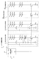
この図に示されるLED駆動回路1では、全部で40個のLED(D10〜D19、D20〜D29、D30〜D39、D40〜D49)を光源として用いることとしている。なお、この場合には、これらのLEDの発光色は、全て白色である。つまり、図14では、白色LEDにより白色光を得るようにされている。そして、図14に示す構成では、これらの40個のLEDを4組に等分して、各組ごとに10個のLEDを割り振り、4つのLED直列回路を形成する。図14に示す第1直列駆動回路部21、第2直列駆動回路部22、第3直列駆動回路部23、第4直列駆動回路部24は、上記4つのLED直列回路を1つずつ備える。
In the
第1直列駆動回路部21は、10個のLED(D10)〜(D19)によるLED直列回路を備える。これらLED(D10)〜(D19)は、それぞれが同じ方向により、順方向に沿って、LED(D10)〜(D19)の順で直列接続されている。
第2直列駆動回路部22は、同じく10個のLED(D20)〜(D29)を、上記第1直列駆動回路部21のLED(D10)〜(D19)に準じて接続したLED直列回路を備える。同様に、第3直列駆動回路部23は、10個のLED(D30)〜(D39)によるLED直列回路を備え、第4直列駆動回路部24は10個のLED(D40)〜(D49)によるLED直列回路を備える。
The first series drive circuit unit 21 includes an LED series circuit including ten LEDs (D10) to (D19). These LEDs (D10) to (D19) are connected in series in the order of the LEDs (D10) to (D19) along the forward direction in the same direction.
Similarly, the second series
そのうえで、第1直列駆動回路部21におけるLED直列回路のアノード側の端部(LED(D10)のアノード)は、定電流回路10の出力端子Doutに対して接続される。同様にして、第2直列駆動回路部22、第3直列駆動回路部23、第4直列駆動回路部24における各LED直列回路のアノード側の端部(LED(D20、D30、D40)のアノード)も、定電流回路10の出力端子Doutに対して接続される
また、第1直列駆動回路部21におけるLED直列回路のカソード側の端部(LED(D19)のカソード)は、トランジスタQ1(コレクターエミッタ)−エミッタ抵抗R11を介してグランドに接続される。同様にして、第2直列駆動回路部22、第3直列駆動回路部23、第4直列駆動回路部24におけるLED直列回路のカソード側の端部(LED(D29、D39、D49)のカソード)も、それぞれ、トランジスタQ2−エミッタ抵抗R21、トランジスタQ3−エミッタ抵抗R31、トランジスタQ4−エミッタ抵抗R41を介してグランドに接続される。
このような接続態様によれば、第1直列駆動回路部21、第2直列駆動回路部22、第3直列駆動回路部23、第4直列駆動回路部24のLED直列回路は、定電流回路10の出力端子Doutに対して並列に接続されているものとみることができる。
In addition, the anode side end of the LED series circuit (the anode of the LED (D10)) in the first series drive circuit unit 21 is connected to the output terminal Dout of the constant
According to such a connection mode, the LED series circuit of the first series drive circuit unit 21, the second series
また、第1直列駆動回路部21、第2直列駆動回路部22、第3直列駆動回路部23、第4直列駆動回路部24において備えられるNPNのトランジスタQ1、Q2、Q3、Q4は、第1直列駆動回路部21を基準とするカレントミラー回路を形成するために設けられる。このために、トランジスタQ1、Q2、Q3、Q4は、例えば同一規格品を選定するなどして、同等の特性を有するようにされている。
第1直列駆動回路部21において、トランジスタQ1のコレクタは、LED直列回路のカソード側の端部(LED(D19)のカソード)と接続される。トランジスタQ1のベースは、この場合には、コレクタに接続される。これにより、トランジスタQ1のベースとコレクタは同電位となる。トランジスタQ1のエミッタは、抵抗R11の一端と接続される。抵抗R11の他端はグランドに接続される。また、この第1直列駆動回路部21におけるエミッタ抵抗R11とトランジスタQ1のエミッタとの接続点は、定電流回路のフィードバック(帰還)端子FBと接続される。
The NPN transistors Q1, Q2, Q3, and Q4 provided in the first series drive circuit unit 21, the second series
In the first series drive circuit unit 21, the collector of the transistor Q1 is connected to the cathode side end of the LED series circuit (the cathode of the LED (D19)). The base of the transistor Q1 is in this case connected to the collector. As a result, the base and collector of the transistor Q1 have the same potential. The emitter of the transistor Q1 is connected to one end of the resistor R11. The other end of the resistor R11 is connected to the ground. Further, the connection point between the emitter resistor R11 and the emitter of the transistor Q1 in the first series drive circuit unit 21 is connected to the feedback terminal FB of the constant current circuit.
また、第2直列駆動回路部22におけるトランジスタQ2のコレクタは、LED直列回路の
カソード側の端部(LED(D29)のカソード)と接続され、エミッタは、エミッタ抵抗R21を介してグランドと接続される。同様にして、第3直列駆動回路部23におけるトランジスタQ3のコレクタは、LED直列回路のカソード側の端部(LED(D39)のカソード)と接続され、エミッタは、エミッタ抵抗R31を介してグランドと接続され、第4直列駆動回路部24におけるトランジスタQ4のコレクタは、LED直列回路のカソード側の端部(LED(D49)のカソード)と接続され、エミッタは、エミッタ抵抗R41を介してグランドと接続される。なお、これら4本のエミッタ抵抗R11、R21、R31、R41については同じ抵抗値を選定すればよい。そのうえで、トランジスタQ2、Q3、Q4のベースは、トランジスタQ1のベースに対して共通に接続される。
Further, the collector of the transistor Q2 in the second series
定電流回路10は、この場合には、例えば定電流電源用ICとして構成される。この定電流回路10は、電源入力端子Dinから直流電源Viを入力し、フィードバック端子FBに入力される検出レベルに基づいて、出力端子Doutから一定量の電流が出力されるように動作する。この出力端子Doutの電圧についてはVoにより示す。
In this case, the constant
上記図14に示すLED駆動回路1の構成では、第1直列駆動回路部21における抵抗R11の両端電圧が定電流回路10のフィードバック端子FBに入力されている。つまり、定電流回路10のフィードバック端子FBには、第1直列駆動回路部21に流れている電流量に対応する電圧レベルが入力されることになる。定電流回路10では、このようにして、フィードバック端子FBに入力される電圧レベルに基づいて、予め設定された定電流レベルの誤差を検出し、この誤差が0となるようにして出力端子Doutから出力すべき電流レベル(電流量)を可変する。このようにして、定電流回路10は、第1直列駆動回路部21を対象として、この第1直列駆動回路部21に流す電流量が一定となるように動作する。
In the configuration of the
そのうえで、この図に示す構成では、前述した回路構成により、トランジスタQ1,Q2、Q3,Q4を備えるカレントミラー回路が形成されている。このようにして構成されるカレントミラー回路では、トランジスタQ1に追従するようにして、トランジスタQ2、Q3、Q4のベース電位を同じとするように動作する。このために、トランジスタQ2、Q3、Q4は、トランジスタQ1と同じベース電流量による増幅動作が行われることとなって、トランジスタQ1と同じレベルのコレクタ電流を流すようにされる。この結果、第1直列駆動回路部21を基準として、第2直列駆動回路部22、第3直列駆動回路部23、及び第4直列駆動回路部24のそれぞれに流れる電流量は同じとなる。
このようにして、LED駆動回路1では、第1直列駆動回路部21を対象として、定電流回路10が、この第1直列駆動回路部21に対して定電流を定常的に流すようにして動作する。そしてさらに、カレントミラー回路により、この基準となる第1直列駆動回路部21と同じ量の電流が、第2直列駆動回路部22、第3直列駆動回路部23、第4直列駆動回路部24にも流れるようにされる。
このことは、第1直列駆動回路部21におけるLED直列回路(D10〜D19)を基準として、先ず、この第1直列駆動回路部21におけるLED直列回路に対して定電流を流すようにしたうえで、残る第2直列駆動回路部22、第3直列駆動回路部23、第4直列駆動回路部24におけるLED直列回路(D20〜D29、D30〜D39、D40〜D49)に対しても、第1直列駆動回路部21におけるLED直列回路と同じ量の電流を流すようにしている、ということを意味する。この結果、LED駆動回路1全体において備えられる40個のLED(D10〜D19、D20〜D29、D30〜D39、D40〜D49)に流れる電流レベルは同等となり、これらのLEDの発光輝度についてもばらつきが解消、抑制されて一定化する。
このようにして、図14に示した回路では、定電流出力に対してLED直列回路を並列接続することで、高圧駆動となる問題を回避したうえで、定電流回路とカレントミラー回路の組み合わせによりLEDごとに流すべき電流量が同じになるようにしている。なお、定電流回路を、並列関係にあるLED直列回路(直列駆動回路部)ごとに設けることによっても、LEDごとに流すべき電流量は一定とすることができる。しかしながら、この場合には、LED直列回路(直列駆動回路部)の数に対応した定電流回路を設ける必要があり、その分の回路規模の拡大やコストアップを招く。図14に示すようにして、1つの定電流回路とカレントミラー回路とを組み合わせるほうが、回路規模の縮小やコストの面では有利である。カレントミラー回路は、例えば図14にも示しているように、LED直列回路(直列駆動回路部)ごとに1石のトランジスタとエミッタ抵抗を備える程度の簡易な回路構成である。
In addition, in the configuration shown in this figure, a current mirror circuit including transistors Q1, Q2, Q3, and Q4 is formed by the circuit configuration described above. The current mirror circuit configured as described above operates so that the base potentials of the transistors Q2, Q3, and Q4 are the same so as to follow the transistor Q1. For this reason, the transistors Q2, Q3, and Q4 perform the amplification operation with the same base current amount as that of the transistor Q1, so that the collector current of the same level as that of the transistor Q1 flows. As a result, the amount of current flowing through each of the second series
In this way, in the
This is based on the LED series circuit (D10 to D19) in the first series drive circuit unit 21, and first a constant current is passed through the LED series circuit in the first series drive circuit unit 21. The LED series circuits (D20 to D29, D30 to D39, D40 to D49) in the remaining second series
In this way, in the circuit shown in FIG. 14, the LED series circuit is connected in parallel to the constant current output, thereby avoiding the problem of high voltage driving, and by combining the constant current circuit and the current mirror circuit. The amount of current to be passed for each LED is the same. It should be noted that the amount of current that should be allowed to flow for each LED can also be made constant by providing a constant current circuit for each LED series circuit (series drive circuit unit) in parallel. However, in this case, it is necessary to provide a constant current circuit corresponding to the number of LED series circuits (series drive circuit units), which causes an increase in circuit scale and cost. As shown in FIG. 14, combining one constant current circuit and a current mirror circuit is more advantageous in terms of circuit scale reduction and cost. For example, as shown in FIG. 14, the current mirror circuit has a simple circuit configuration that includes one transistor and an emitter resistor for each LED series circuit (series drive circuit section).
しかしながら、上記図14に示した構成のままのLED駆動回路1では、現実には次のような不都合がある。
LEDには順方向降下電圧(Vf)が存在することは周知であり、この順方向降下電圧としては、平均で3.5V程度である。しかし、この3.5Vという値は、あくまでも平均であり、現実のLEDにあっては、3.0V程度から4.0V程度の間でのばらつきのあることが知られている。
However, the
It is well known that the LED has a forward voltage drop (Vf), and the forward voltage drop is about 3.5 V on average. However, this value of 3.5V is only an average, and it is known that there is a variation between about 3.0V and about 4.0V in an actual LED.
ここで、説明を簡単にするために、LEDの順方向降下電圧のばらつきの下限値を3.0V、上限値を4.0Vとして、LED駆動回路1を構成する場合を想定してみる。LED駆動回路1は、LED直列回路を10個のLEDにより形成しているので、1つのLED直列回路あたりの順方向降下電圧の下限値は、30V(3.0×10)であり、上限値は40V(4.0×10)となる。つまり、LED駆動回路1を実際に構成するのにあたって、1つのLED直列回路の電圧降下については、30V〜40Vの範囲でのばらつきが存在する可能性があることになる。
Here, in order to simplify the description, it is assumed that the
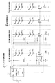
そこで、図14には、1つのLED直列回路の電圧降下が下限値の30Vと上限値の40Vとで偏った場合として、基準となる側の第1直列駆動回路部21のLED直列回路の電圧降下が40Vで、追従する側の第2直列駆動回路部22のLED直列回路の電圧降下が30Vとなる場合を示している。
この場合の第1直列駆動回路部21においては、上記のようにしてLED直列回路の電圧降下は40Vである。また、トランジスタQ1のベースはコレクタと接続されていることで、トランジスタQ1のコレクタ電位は、ベース電位と同じになる。ここで、トランジスタQ1のベース−エミッタ間電圧(VBE1)については0.7Vであるとすると、トランジスタQ1のコレクタ−エミッタ間電圧(VCE1)も0.7Vとなる。また、エミッタ抵抗R11の両端電圧に相当するエミッタ電位は、ここでは0.3Vとなるようにしてエミッタ抵抗R11の抵抗値が選定されているものとする。
すると、第1直列駆動回路部21全体としては、40V、0.7V、0.3Vの電圧降下が存在することとなって、第1直列駆動回路部21全体の両端にかかる電圧、つまり、定電流回路10の出力端子Doutにおいて生じる電圧Voとしては、
Vo=41V(=40+0.7+0.3)
であることになる。
Therefore, FIG. 14 shows the voltage of the LED series circuit of the first series drive circuit unit 21 on the reference side as a case where the voltage drop of one LED series circuit is biased between the lower limit value of 30V and the upper limit value of 40V. The case where the voltage drop is 40V and the voltage drop of the LED series circuit of the second series
In the first series drive circuit unit 21 in this case, the voltage drop of the LED series circuit is 40V as described above. Further, since the base of the transistor Q1 is connected to the collector, the collector potential of the transistor Q1 becomes the same as the base potential. Here, assuming that the base-emitter voltage (VBE1) of the transistor Q1 is 0.7V, the collector-emitter voltage (VCE1) of the transistor Q1 is also 0.7V. It is assumed that the resistance value of the emitter resistor R11 is selected so that the emitter potential corresponding to the voltage across the emitter resistor R11 is 0.3V.
As a result, voltage drops of 40 V, 0.7 V, and 0.3 V exist in the entire first series drive circuit unit 21, and the voltage applied to both ends of the entire first series drive circuit unit 21, that is, a constant current circuit. As the voltage Vo generated at the ten output terminals Dout,
Vo = 41V (= 40 + 0.7 + 0.3)
It will be.
このVo=41Vの電圧は、第1直列駆動回路部21に追従する側の第2直列駆動回路部22の両端にもかかることになる。この第2直列駆動回路部22におけるLED直列回路の電圧降下は、30Vである。
また、トランジスタQ2とトランジスタQ1のベースは接続されて同電位であるので、エミッタ電位(抵抗R21の両端電圧)は、第1直列駆動回路部21と同様に0.3Vとなる。この状態では、トランジスタQ2のコレクタ−エミッタ間電圧(VCE2)は、VCE2=10.7V(=41−(30+0.3))となる。
The voltage of Vo = 41V is also applied to both ends of the second series
Further, since the bases of the transistor Q2 and the transistor Q1 are connected and have the same potential, the emitter potential (the voltage across the resistor R21) is 0.3 V, as in the first series drive circuit section 21. In this state, the collector of the transistor Q2 - emitter voltage (VCE2) is, VCE2 = 10.7 V - a (= 41 (30 + 0.3)).
この場合においては、トランジスタQ1のコレクタ電圧、ベース電圧は、1V(=0.7+0.3)であるのに対して、トランジスタQ2のコレクタ電圧は11V(=10.7+0.3)となる。このときには、トランジスタQ2は、不飽和領域にて正常に動作する条件を満たしていることになる。つまり、カレントミラー回路は通常に動作するものであり、ここでは特に問題を生じない。 In this case, the collector voltage and base voltage of the transistor Q1 are 1V (= 0.7 + 0.3), whereas the collector voltage of the transistor Q2 is 11V (= 10.7 + 0.3). At this time, the transistor Q2 satisfies the condition for operating normally in the unsaturated region. That is, the current mirror circuit operates normally and does not cause any particular problem here.
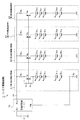
これに対して、図14の場合とは逆に、1つのLED直列回路の電圧降下が最小値の30Vと最大値の40Vとで偏った場合として、基準となる第1直列駆動回路部21のLED直列回路の電圧降下が30V、第2直列駆動回路部22のLED直列回路の電圧降下が40Vとなる場合を、図15に示す。
On the other hand, as opposed to the case of FIG. 14, the voltage drop of one LED series circuit is biased between the minimum value of 30V and the maximum value of 40V. FIG. 15 shows a case where the voltage drop of the LED series circuit is 30V and the voltage drop of the LED series circuit of the second series
この場合の第1直列駆動回路部21においては、LED直列回路における30Vの電圧降下と、トランジスタQ1のトランジスタQ1のベース−エミッタ間電圧(VBE1)、コレクタ−エミッタ間電圧(VCE1)としての0.7Vの電圧降下と、エミッタ電圧(エミッタ抵抗R11の両端電圧)としての0.3Vの電圧降下が存在する。このため、第1直列駆動回路部21全体の両端にかかる電圧Voは、Vo=31V(=30+0.7+0.3)であることになる。 In the first series drive circuit unit 21 in this case, a voltage drop of 30V in the LED series circuit, a base-emitter voltage (VBE1) of the transistor Q1 of the transistor Q1, and a collector-emitter voltage (VCE1) of 0.7V. And a voltage drop of 0.3 V as an emitter voltage (a voltage across the emitter resistor R11). For this reason, the voltage Vo applied to both ends of the entire first series drive circuit unit 21 is Vo = 31 V (= 30 + 0.7 + 0.3).
この電圧Vo=31Vの電位は、第1直列駆動回路部21に追従する側の第2直列駆動回路部22の両端にもかかることになる。
しかしこの場合、第2直列駆動回路部22におけるLED直列回路の電圧降下は40Vである。トランジスタQ2のエミッタ電圧(抵抗R21の両端電圧)は、第1直列駆動回路部21と同様に0.3Vである。従って、この場合においては、トランジスタQ2のコレクタ−エミッタ間電圧(VCE2)は、-9.3V(=31−(40+0.3))となる。つまり、この場合には、コレクタ−エミッタ間電圧(VCE1)は、計算上は負の値をとることになる。このような電位の状態では、トランジスタQ2は、不飽和領域での正常な動作が得られなくなる。この場合には、カレントミラー回路としての通常の動作が得られないこととなって、例えば第2直列駆動回路部22に対して、第1直列駆動回路部21と同量の電流を流すことができなくなる。
The potential of the voltage Vo = 31V is also applied to both ends of the second series
However, in this case, the voltage drop of the LED series circuit in the second series
このように図14(図15)に示したようにして、単に定電流回路とカレントミラー回路とを組み合わせた構成のLED駆動回路では、実際におけるLEDの順方向降下電圧のばらつきを考慮したときに、正常な動作が保証できない場合があるという、実用上での問題を抱えている。 As described above with reference to FIG. 14 (FIG. 15), in the LED driving circuit having a configuration in which the constant current circuit and the current mirror circuit are simply combined, when the variation in the actual forward voltage drop of the LED is taken into consideration, There is a practical problem that normal operation cannot be guaranteed.
そこで、本願の発明を実施するための最良の形態(実施の形態)としては、上記したようなLEDの順方向降下電圧のばらつきを吸収して、正常なカレントミラー回路の動作が得られるようにされたLED駆動回路1を提供する。
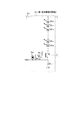
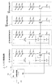
図1は、第1の実施の形態としてのLED駆動回路1の構成例を示している。なお、この図において、図14、図15と同一部分には同一符号を付して、ここでの詳細な説明は省略する。
この図1に示すLED駆動回路1の構成としては、第1直列駆動回路部21において備えられる電圧降下回路部11を省略すれば、先に図14,図15に示したLED駆動回路と同じ回路構成となる。つまり、LED駆動回路1の基本構成としても、それぞれ10個のLEDを直列接続した第1〜第4直列駆動回路部21〜24を備え、定電流回路10の出力に対して並列に接続する。そして、定電流回路10は、基準となる第1直列駆動回路部21において検出抵抗R11により検出される電流量に基づいて、第1直列駆動回路部21に対して所要の一定量の電流を流すように動作する。さらに、第1〜第4直列駆動回路部21〜24に対してそれぞれトランジスタQ1〜Q4を備えてカレントミラー回路を形成することで、第2〜第4直列駆動回路部22〜24に流れる電流が、第1直列駆動回路部21に流れる電流と同じになるようにする。
Therefore, the best mode (embodiment) for carrying out the invention of the present application is to absorb the variation in the forward voltage drop of the LED as described above and to obtain a normal operation of the current mirror circuit. Provided is the
FIG. 1 shows an example of the configuration of an
The configuration of the
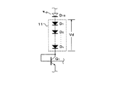
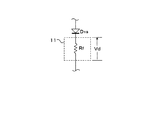
そのうえで、この図に示すLED駆動回路1では、第1直列駆動回路部21において、LED直列回路(D10〜D19)に対して直列となる関係により、電圧降下回路部11を挿入することとしている。この場合の電圧降下回路部11の挿入位置としては、LED直列回路(D10〜D19)におけるLED(D19)のカソード端部と、トランジスタQ1のコレクタとの間のラインとなっている。この電圧降下回路部11は、第1直列駆動回路部21において所定レベルによる電圧降下(降下電圧Vd)を発生させるために設けられる。
In addition, in the
ここで、説明を分かりやすいものとするために、電圧降下回路部11の構成の一例を、図2に示しておく。なお、他の構成例については後述する。
図2に示す電圧降下回路部11は、所定数のダイオード素子D1〜Dnを、LED直列回路と同じ順方向に従って直列接続して形成されている。この場合において、電圧降下回路部11として備えられるダイオード素子の数は1以上とされ、実際に必要とされる降下電圧Vdに応じた数を用意して直列に接続すればよい。このようにして、図2では、ダイオード素子を電圧降下用素子として機能させる。ダイオード素子1つあたりの順方向降下電圧は、0.65V程度であることから、ダイオード素子D1〜Dnの数に応じて、Vd=0.65×nで表される降下電圧Vdを発生させることができる。
Here, in order to make the explanation easy to understand, an example of the configuration of the voltage drop circuit unit 11 is shown in FIG. Other configuration examples will be described later.
The voltage drop circuit unit 11 shown in FIG. 2 is formed by connecting a predetermined number of diode elements D1 to Dn in series according to the same forward direction as the LED series circuit. In this case, the number of diode elements provided as the voltage drop circuit unit 11 is one or more, and a number corresponding to the actually required drop voltage Vd may be prepared and connected in series. In this way, in FIG. 2, the diode element functions as a voltage drop element. Since the forward drop voltage per diode element is about 0.65 V, a drop voltage Vd represented by Vd = 0.65 × n can be generated according to the number of diode elements D1 to Dn.
例えば上記のようにして構成できる電圧降下回路部11を挿入した本実施の形態のLED駆動回路1の動作について説明する。
ここでの説明にあたり、第1直列駆動回路部21のLED直列回路(D10〜D19)による電圧降下は、ばらつきにおける下限値となる30Vであり、第2直列駆動回路部22のLED直列回路(D20〜D29)による電圧降下は、ばらつきにおける上限値となる40Vであることとする。つまり、第1直列駆動回路部21のLED直列回路(D10〜D19)と第2直列駆動回路部22のLED直列回路(D20〜D29)との電圧降下レベルの関係は、先に図15に示した場合と同様であることとしている。確認のために述べておくと、図15の回路構成において、このばらつきの組み合わせでは、第2直列駆動回路部22におけるトランジスタQ2のコレクタ電圧が正常でなくなり、適正なカレントミラー回路の動作が期待できない。
また、電圧降下回路部11により生じる降下電圧Vdは、10Vであることとする。例えば、実際に図2に示したようにしてダイオード素子により電圧降下回路部11を構成した場合には、ダイオード素子1つあたりの順方向降下電圧が約0.65Vなので、降下電圧Vdが、ちょうど10Vとなることはないのであるが、ここでは説明をわかりやすいものとするために、10Vを設定している。
For example, the operation of the
In the description here, the voltage drop due to the LED series circuit (D10 to D19) of the first series drive circuit unit 21 is 30 V, which is the lower limit value in the variation, and the LED series circuit (D20 of the second series drive circuit unit 22). The voltage drop due to D29) is assumed to be 40 V which is the upper limit value in the variation. That is, the relationship of the voltage drop level between the LED series circuit (D10 to D19) of the first series drive circuit unit 21 and the LED series circuit (D20 to D29) of the second series
The voltage drop Vd generated by the voltage drop circuit unit 11 is 10V. For example, when the voltage drop circuit unit 11 is configured by diode elements as shown in FIG. 2, the forward drop voltage per diode element is about 0.65 V, so the drop voltage Vd is exactly 10 V. However, in order to make the explanation easy to understand, 10V is set here.
この場合の第1直列駆動回路部21においては、LED直列回路における30Vの電圧降下と、トランジスタQ1のベース−エミッタ間電圧(VBE1)、コレクタ−エミッタ間電圧(VCE1)としての0.7Vの電圧降下と、エミッタ電圧(エミッタ抵抗R11の両端電圧)としての0.3Vの電圧降下に加えて、電圧降下回路部11による10Vの電圧降下が存在する。従って、第1直列駆動回路部21全体の両端にかかる電圧Voは、Vo=41V(=30+0.7+0.3+10)で表されることになる。 In the first series drive circuit unit 21 in this case, a voltage drop of 30 V in the LED series circuit and a voltage drop of 0.7 V as the base-emitter voltage (VBE1) and collector-emitter voltage (VCE1) of the transistor Q1. In addition to the voltage drop of 0.3V as the emitter voltage (the voltage across the emitter resistor R11), there is a voltage drop of 10V due to the voltage drop circuit unit 11. Therefore, the voltage Vo applied to both ends of the entire first series drive circuit unit 21 is expressed by Vo = 41V (= 30 + 0.7 + 0.3 + 10).
この電圧Vo=41Vは、第2直列駆動回路部22にもかかることになる。
このことから、第2直列駆動回路部22におけるトランジスタQ2のコレクタ−エミッタ間電圧(VCE2)を求めてみると、LED直列回路(D20〜D29)による電圧降下が40V、エミッタ抵抗R21による電圧降下が0.3Vであるから、VCE2=0.7V(=41−(40+0.3))で表されることになる。
This voltage Vo = 41V is also applied to the second series
From this, when the collector-emitter voltage (VCE2) of the transistor Q2 in the second series
すると、この場合の第1直列駆動回路部21におけるトランジスタQ1のコレクタ電圧は、1V(=0.7+0.3)であるのに対して、第2直列駆動回路部22におけるトランジスタQ2のコレクタ電圧も1V(=0.7+0.3)である。つまり、トランジスタQ1、Q2のコレクタ電圧は同等になっている。このことは、カレントミラー回路が正常に動作し、第2直列駆動回路部22に対しても、第1直列駆動回路部21と同量の電流が流されることを意味する。また、例えば、第2直列駆動回路部22に代えて、第3直列駆動回路部23におけるLED直列回路の電圧降下が40Vである場合においても、上記したのと同様の電圧降下の状態が生じることから、トランジスタQ1、Q3のコレクタ電圧は同等になり、正常なカレントミラー回路の動作が得られる。本実施の形態のLED駆動回路1は、基準となる第1直列駆動回路部21におけるLED直列回路の電圧降下が小さく、他の追従側の第2直列駆動回路部22、第3直列駆動回路部23、第4直列駆動回路部24の何れかにおおけるLED直列回路の電圧降下のほうが大きくなるようなばらつきの状態にあっても、カレントミラー回路の正常な動作を維持することが可能になるものである。
Then, in this case, the collector voltage of the transistor Q1 in the first series drive circuit unit 21 is 1V (= 0.7 + 0.3), whereas the collector voltage of the transistor Q2 in the second series
ここで、電圧降下回路部11としての構成について、図2に示した以外の構成例を、図3〜図5に示す。
図3では、LEDを電圧降下用素子として使用するもので、必要数のLED(DL1〜DLn)を、LED直列回路と同じ順方向に従って直列接続することで、電圧降下回路部11を形成している。この場合においても、電圧降下回路部11として備えられるLEDの数は1以上であって、実際に必要とされる降下電圧Vdに応じた数を用意して直列に接続すればよい。ちなみに、1つのLEDあたりの順方向降下電圧は、一般には3.2V〜3.6V程度である。
Here, with respect to the configuration as the voltage drop circuit unit 11, configuration examples other than those shown in FIG. 2 are shown in FIGS.
In FIG. 3, the LED is used as a voltage drop element, and the voltage drop circuit unit 11 is formed by connecting the necessary number of LEDs (DL1 to DLn) in series according to the same forward direction as the LED series circuit. Yes. Even in this case, the number of LEDs provided as the voltage drop circuit unit 11 is one or more, and a number corresponding to the actually required drop voltage Vd may be prepared and connected in series. Incidentally, the forward drop voltage per LED is generally about 3.2V to 3.6V.
また、図4は、電圧降下回路部11として、1石のトランジスタQ10を備えた簡易な定電圧回路を備えた構成を示している。この場合のトランジスタQ10はNPNであり、コレクタを、ダイオード素子D19のカソード側と接続し、エミッタをトランジスタQ1のコレクタと接続する。そして、トランジスタQ10のコレクタ−ベース間に対して抵抗RB1を接続し、ベース−エミッタ間に対して抵抗RB2を接続する。 FIG. 4 shows a configuration including a simple constant voltage circuit including a single transistor Q10 as the voltage drop circuit unit 11. In this case, the transistor Q10 is NPN, and has a collector connected to the cathode side of the diode element D19 and an emitter connected to the collector of the transistor Q1. A resistor RB1 is connected between the collector and base of the transistor Q10, and a resistor RB2 is connected between the base and emitter.
この構成において、先ず、NPNであるトランジスタQ10のベース−エミッタ間電圧(VBE10)は0.6〜0.7V程度となるが、VBE10=0.6Vであるとすると、トランジスタQ10のコレクタ−エミッタ間電圧(VCE10)は、
VCE10=0.6×(RB1+RB2)/RB2・・・(式1)
で表され一定レベルを有することになる。つまり、トランジスタQ10のコレクタ−エミッタ間電圧(VCE10)としての一定電圧レベルは、抵抗RB1、RB2の抵抗値により、任意に可変して設定できる。この図に示す構成では、上記のようにして設定されるトランジスタQ10のコレクタ−エミッタ間電圧(VCE10)が降下電圧Vdとなる。
In this configuration, first, the base-emitter voltage (VBE10) of the transistor Q10, which is an NPN, is about 0.6 to 0.7V. If VBE10 = 0.6V, the collector-emitter voltage of the transistor Q10 The voltage (VCE10) is
VCE10 = 0.6 × (RB1 + RB2) / RB2 (Formula 1)
And has a certain level. That is, the constant voltage level as the collector-emitter voltage (VCE10) of the transistor Q10 can be arbitrarily variably set according to the resistance values of the resistors RB1 and RB2. In the configuration shown in this figure, the collector-emitter voltage (VCE10) of the transistor Q10 set as described above becomes the drop voltage Vd.
図5に示す電圧降下回路部11は、降下電圧Vdを得るのに必要な抵抗値を有する抵抗素子Rfを、電圧降下用素子として挿入した構成である。 The voltage drop circuit unit 11 shown in FIG. 5 has a configuration in which a resistance element Rf having a resistance value necessary to obtain the drop voltage Vd is inserted as a voltage drop element.
例えば、図3に示したように電圧降下回路部11では、当然のこととして、第1直列駆動回路部21に対して電圧Voのラインから駆動電流が流れたときには、この電圧降下回路部11としての部位のLED(DL1〜DLn)も発光駆動される。このことから、図3に示すようにして、電圧降下回路部11において備えられる電圧降下用素子としてLEDを採用する場合には、本来の光源用のLED(D10〜D19)などと同様にして、電圧降下用素子のLEDについても光源として有効に利用できる。
ただし、LED1つあたりの順方向降下電圧は、3.2V〜3.6V程度である。例えばLED1つあたりの順方向降下電圧について3.5Vとすると、直列接続するLEDの個数の増加に応じては、例えば3.5V、7V、10.5Vというように3.5V程度の間隔での降下電圧の増加になる。このようにして3.5V程度となる電圧降下の変更幅は、実際の定電流回路10における駆動電圧が数十Vのオーダーであることなどを考慮すると、比較的に大きいものであるということがいえる。このために、実際に設定する駆動電圧などとの兼ね合いでは、3.5V程度となる電圧降下の変更幅では、適切な降下電圧Vdの調整を行うことが難しい場合がある。
これに対して、先に図2に示したダイオード素子を直列接続する構成であれば、ダイオード素子1つあたりの順方向降下電圧は0.65V程度であり、LEDと比較してはるかに小さい。このために、降下電圧Vdについてのより細かな調整が行えるという利点がある。
For example, as shown in FIG. 3, in the voltage drop circuit unit 11, as a matter of course, when a drive current flows from the line of voltage Vo to the first series drive circuit unit 21, the voltage drop circuit unit 11 The LEDs (DL1 to DLn) in the region are also driven to emit light. Therefore, as shown in FIG. 3, when an LED is used as a voltage drop element provided in the voltage drop circuit unit 11, it is the same as the original light source LED (D10 to D19), etc. The LED of the voltage drop element can also be effectively used as a light source.
However, the forward voltage drop per LED is about 3.2V to 3.6V. For example, if the forward voltage drop per LED is 3.5V, the voltage drops at intervals of about 3.5V, such as 3.5V, 7V, 10.5V, etc., as the number of LEDs connected in series increases. Increase in voltage. In this way, the change width of the voltage drop to be about 3.5V is relatively large considering that the drive voltage in the actual constant
In contrast, if the diode elements shown in FIG. 2 are connected in series, the forward voltage drop per diode element is about 0.65 V, which is much smaller than that of the LED. For this reason, there is an advantage that finer adjustment of the drop voltage Vd can be performed.
また、図2、図3に示した電圧降下回路部11の構成として、実際に、複数個のダイオード素子、あるいは複数個のLEDを直列接続した場合において、例えば後において、何らかの事情で、降下電圧Vdを小さくしたいような場合には、ダイオード素子、あるいはLEDを必要数取り除くことができ、簡易な作業で対応できる。 In addition, as a configuration of the voltage drop circuit unit 11 shown in FIGS. 2 and 3, when a plurality of diode elements or a plurality of LEDs are actually connected in series, for example, for some reason, a voltage drop When it is desired to reduce Vd, the required number of diode elements or LEDs can be removed, and this can be handled with a simple operation.
また、図4に示したような定電圧回路を電圧降下回路部11として備える構成については、抵抗RB1、RB2の変更によって、リニアに近いとされる変更幅でもって、降下電圧Vdの調整を行うことが可能である。 Further, in the configuration including the constant voltage circuit as shown in FIG. 4 as the voltage drop circuit unit 11, the drop voltage Vd is adjusted with a change width assumed to be linear by changing the resistors RB1 and RB2. It is possible.
また、図5に示した、抵抗Rfを挿入する構成は、これまでに示した電圧降下回路部11の構成例のうちで、最も簡易であり、例えば部品コストなどに関して有利となる。 Further, the configuration in which the resistor Rf is inserted as shown in FIG. 5 is the simplest of the configuration examples of the voltage drop circuit unit 11 shown so far, and is advantageous in terms of component costs, for example.
なお、1つの電圧降下回路部11として、例えば上記図2〜図5に示した電圧降下用素子、回路の全て、あるいは一部を併用して組み合わせて構成することも考えられる。一例として、図2に示したダイオード素子と図3に示したLEDを混在させた直列接続回路により電圧降下回路部11を形成することができる。 One voltage drop circuit unit 11 may be configured by combining all or part of the voltage drop elements and circuits shown in FIGS. 2 to 5, for example. As an example, the voltage drop circuit unit 11 can be formed by a series connection circuit in which the diode element shown in FIG. 2 and the LED shown in FIG. 3 are mixed.
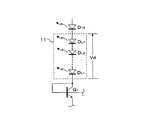
また、図6は、第1の実施の形態における電圧降下回路部11の挿入形態についての変形例である。なお、この図には第1直列駆動回路部21のみが示されているが、これ以外の部位は図1と同様とされる。
この図においては、第1直列駆動回路部21において、電圧降下回路部11を、電圧Voのラインと、LED直列回路のアノード側端部となる、LED(D10)のアノードとの間に挿入している。確認のために、このときの電圧降下回路部11の構成は、図2、図3、図4、図5に示した構成のうちの何れが採用されてもよい。
このような電圧降下回路部11の挿入位置とした場合にも、電圧降下回路部11の電圧降下により電圧Voの引き上げが行われる分、追従側の第2〜第4直列駆動回路部22〜24のトランジスタQ1,Q2、Q3のコレクタ電圧が引き上げられるものであり、図1の場合と同様にして適正なカレントミラー回路の動作が得られる。
また、図示は省略するが、電圧降下回路部11は、例えばLED直列回路(D10〜D19)における任意のLEDのアノードとカソードの接続点に対して挿入してもよいものである。実際における電圧降下回路部11の挿入位置は、例えば、光源装置に本実施の形態のLED駆動回路1を組み込んだときにおけるLEDや回路の物理的配置などに応じて決めるようにすることができる。
FIG. 6 is a modification of the insertion form of the voltage drop circuit unit 11 in the first embodiment. Although only the first series drive circuit unit 21 is shown in this figure, the other parts are the same as those in FIG.
In this figure, in the first series drive circuit unit 21, the voltage drop circuit unit 11 is inserted between the line of the voltage Vo and the anode of the LED (D10) which becomes the anode side end of the LED series circuit. ing. For confirmation, any of the configurations shown in FIGS. 2, 3, 4, and 5 may be employed as the configuration of the voltage drop circuit unit 11 at this time.
Even in the insertion position of the voltage drop circuit unit 11, the second to fourth series
Moreover, although illustration is abbreviate | omitted, the voltage drop circuit part 11 may be inserted with respect to the connection point of the anode and cathode of arbitrary LED in LED series circuit (D10-D19), for example. The actual insertion position of the voltage drop circuit unit 11 can be determined according to, for example, the physical arrangement of the LEDs and circuits when the
また、図7には、第1の実施の形態における電圧降下回路部11の挿入形態についての他の変形例を示している。なお、この図においても、図6と同様にして、第1直列駆動回路部21のみを示しており、これ以外の部位は図1と同様とされる。
この図では、電圧降下回路部11について分割電圧降下回路部11A,11Bとに分割し、これら分割電圧降下回路部11A,11Bを、それぞれ第1直列駆動回路部21における異なる位置に挿入した構成としている。この図においては、分割電圧降下回路部11Aを、電圧Voのラインと、LED直列回路のアノード側端部となるLED(D10)のアノードとの間に挿入し、分割電圧降下回路部11Bを、LED直列回路のカソード側端部となるLED(D19)のカソードと、トランジスタQ1のコレクタとの間に挿入している。
分割電圧降下回路部11Aにより得られる降下電圧をVd1とし、分割電圧降下回路部11Bにより得られる降下電圧をVd2とすると、第1直列駆動回路部21において必要とされる電圧降下回路部11による総合的な降下電圧Vdは、Vd=Vd1+Vd2により表されることになる。
FIG. 7 shows another modification of the insertion form of the voltage drop circuit unit 11 in the first embodiment. Also in this figure, only the first series drive circuit unit 21 is shown in the same manner as in FIG. 6, and the other parts are the same as in FIG.
In this figure, the voltage drop circuit unit 11 is divided into divided voltage
If the voltage drop obtained by the divided voltage
図7においては、分割電圧降下回路部11A,11Bについて、それぞれ、図2により説明したダイオード素子の直列接続回路(1以上であればよい)を電圧降下用素子として備える構成を採った場合を示している。分割電圧降下回路部11Aは、降下電圧Vd1に対応した所要数のダイオード素子D1〜Dm-1を直列に接続して挿入している。同様にして、分割電圧降下回路部11Bは、降下電圧Vd2に対応した所要数のダイオード素子Dm〜Dnを直列に接続して挿入している。
FIG. 7 shows a case where each of the divided voltage
なお、この場合において、分割電圧降下回路部11A,11Bにおいて実際に設定される降下電圧Vd1,Vd2は等しい必要はない。つまり、図示するようにして、ダイオード素子を電圧降下用素子として使用する場合において、分割電圧降下回路部11A,11Bにおけるダイオード素子の直列接続数は、互いに異なるものであってよい。
また、分割電圧降下回路部の数としても2つに限定されるものではなく、3以上に分割したうえで、第1直列駆動回路部21において駆動電流が流れる任意の位置に挿入するようにしてよい。
In this case, the drop voltages Vd1 and Vd2 actually set in the divided voltage
Also, the number of divided voltage drop circuit units is not limited to two, and is divided into three or more and inserted into an arbitrary position where the drive current flows in the first series drive circuit unit 21. Good.
また、図7では、分割電圧降下回路部11A,11Bとしてダイオード素子を備える構成を示しているが、例えば図3に示したLEDを備える構成も適用できる。また、図4、図5に示した構成も適用できる。
図4の構成を適用する場合には、分割電圧降下回路部として、それぞれ、図4に示すようにして、トランジスタQ10と抵抗RB1、RB2を備えた構成とする。そのうえで、先の(式1)に基づいて、各分割電圧降下回路部において必要な降下電圧(Vd1、Vd2・・)が得られるようにして、抵抗RB1、RB2を選定する。
また、図4に示す構成を適用するのであれば、分割電圧降下回路部ごとに必要とされる降下電圧(Vd1、Vd2・・)に対応する抵抗値の抵抗を選定して挿入することとすればよい。
Further, in FIG. 7, a configuration including a diode element as the divided voltage drop circuit units 11 </ b> A and 11 </ b> B is illustrated, but a configuration including the LED illustrated in FIG. 3 can also be applied. The configurations shown in FIGS. 4 and 5 can also be applied.
When the configuration of FIG. 4 is applied, the divided voltage drop circuit section includes a transistor Q10 and resistors RB1 and RB2, as shown in FIG. In addition, the resistors R B1 and RB2 are selected based on the above (Equation 1) so that necessary voltage drops (Vd1, Vd2,...) Can be obtained in each divided voltage drop circuit unit.
If the configuration shown in FIG. 4 is applied, a resistor having a resistance value corresponding to the drop voltage (Vd1, Vd2,...) Required for each divided voltage drop circuit unit should be selected and inserted. That's fine.
また、図8は、第1の実施の形態におけるカレントミラー回路の回路形態についての変形例を示している。なお、この図において、図1と同一とされる部位については同一符号を付し、同一内容についての説明は省略する。
この図では、カレントミラー回路を形成するためのトランジスタQ1、Q2、Q3、Q4についてPNPとしている。そして、例えば第1直列駆動回路部21では、トランジスタQ1のエミッタを、エミッタ抵抗R11を介して電圧Voのラインと接続し、コレクタをLED直列回路(D10〜D19)におけるアノード側端部(D10のアノード)と接続する。
第2〜第4直列駆動回路部22,23,24では、トランジスタQ2、Q3、Q4について、上記第1直列駆動回路部21と同様の態様により接続する。そのうえで、トランジスタQ1、Q2、Q3、Q4のベースを相互に接続する。
また、この場合には、トランジスタQ1のエミッタ抵抗R11が電圧Voのライン側に接続され、アースに接地されないことから、図1の場合のようにして、エミッタ抵抗R11の両端電圧を、定電流回路10のフィードバック端子FBに入力させる検出電圧として利用することが難しい。そこで、この場合には、電圧降下回路部11とアースとの間に対して検出抵抗Rdを別途設けることとして、駆動電流量を、この検出抵抗Rdの両端電圧として検出して定電流回路10のフィードバック端子FBに入力させることとしている。
FIG. 8 shows a modification of the circuit configuration of the current mirror circuit in the first embodiment. In this figure, parts that are the same as those in FIG. 1 are given the same reference numerals, and descriptions of the same contents are omitted.
In this figure, the transistors Q1, Q2, Q3, and Q4 for forming a current mirror circuit are PNPs. For example, in the first series drive circuit unit 21, the emitter of the transistor Q1 is connected to the line of voltage Vo via the emitter resistor R11, and the collector is connected to the anode side end (D10 of D10) in the LED series circuit (D10 to D19). Anode).
In the second to fourth series
In this case, since the emitter resistor R11 of the transistor Q1 is connected to the line side of the voltage Vo and is not grounded to the ground, the voltage across the emitter resistor R11 is changed to a constant current circuit as in the case of FIG. It is difficult to use as a detection voltage to be input to the 10 feedback terminals FB. Therefore, in this case, the detection resistor Rd is separately provided between the voltage drop circuit unit 11 and the ground, and the amount of drive current is detected as the voltage across the detection resistor Rd to detect the constant
このような構成では、第1〜第4直列駆動回路部21〜24は、定電流回路10の出力である電圧Voのラインに対して並列に接続される。さらに、第1〜第4直列駆動回路部21〜24に対して、PNPトランジスタQ1、Q2、Q3、Q4を備えたカレントミラー回路が形成されることになる。
このような構成であっても、第1直列駆動回路部21においてしかるべき降下電圧Vdが設定された電圧降下回路部11が備えられていることで、第1直列駆動回路部21におけるLED直列回路の電圧降下が他の直列駆動回路部よりも小さくなる状態にかかわらず、トランジスタQ2、Q3、Q4側のコレクタ電圧を適正範囲に保ち、正常なカレントミラー回路の動作を得ることができる。
また、この構成では、検出抵抗Rdにおいても抵抗値に応じた電圧降下が生じることから、この検出抵抗Rdによる電圧降下分を含めて、電圧降下回路部11としての降下電圧Vdとして扱うことができる。このようにして、降下電圧Vdに検出抵抗Rdの要素が含められることで、例えば、電圧降下回路部11自体での降下電圧生成のための負担が軽減する。また、より細かな降下電圧Vdの調整が可能になる。
In such a configuration, the first to fourth series drive circuit units 21 to 24 are connected in parallel to the line of the voltage Vo that is the output of the constant
Even in such a configuration, the LED series circuit in the first series drive circuit unit 21 is provided with the voltage drop circuit unit 11 in which the appropriate voltage drop Vd is set in the first series drive circuit unit 21. Regardless of the state in which the voltage drop is smaller than that of the other series drive circuit sections, the collector voltages on the transistors Q2, Q3, and Q4 sides can be maintained within an appropriate range, and normal current mirror circuit operation can be obtained.
Further, in this configuration, a voltage drop corresponding to the resistance value also occurs in the detection resistor Rd. Therefore, the voltage drop due to the detection resistor Rd can be handled as the drop voltage Vd as the voltage drop circuit unit 11. . Thus, by including the element of the detection resistor Rd in the drop voltage Vd, for example, the burden for generating the drop voltage in the voltage drop circuit unit 11 itself is reduced. In addition, the voltage drop Vd can be adjusted more finely.
続いて、第2の実施の形態について説明を行っていくこととするが、第2の実施の形態の構成について説明するのに先立ち、図9を参照して、図1に示した第1の実施の形態のLED駆動回路1について下記の条件での動作を考察してみる。
この図9においては、条件として、LEDの電圧降下のばらつきが3.0V〜4.0Vの範囲であるものと想定し、さらに、第1直列駆動回路部21におけるLED直列回路(D10〜D19)による全体の電圧降下がばらつき範囲の上限となる40V(=4.0×10)であるのに対して、第2直列駆動回路部22におけるLED直列回路(D20〜D29)による全体の電圧降下が、ばらつき範囲の下限となる30V(=3.0×10)であるとする。また、電圧降下回路部11、トランジスタQ1、エミッタ抵抗R11による降下電圧は、それぞれ、図1の場合と同様であるものとする。
Subsequently, the second embodiment will be described. Prior to describing the configuration of the second embodiment, referring to FIG. 9, the first embodiment shown in FIG. Consider the operation of the
In FIG. 9, it is assumed that the variation of the LED voltage drop is in the range of 3.0V to 4.0V as a condition, and further, the entire LED series circuit (D10 to D19) in the first series drive circuit unit 21. Is 40 V (= 4.0 × 10), which is the upper limit of the variation range, whereas the overall voltage drop due to the LED series circuit (D20 to D29) in the second series
すると、第1直列駆動回路部21においては、LED直列回路(D10〜D19)による40Vの電圧降下と、電圧降下回路部11による10Vの電圧降下と、トランジスタQ1のコレクタ−エミッタ間電圧(VCE1)による0.7Vの電圧降下と、エミッタ抵抗R11による0.3Vの電圧降下が存在することとなるので、第1直列駆動回路部21にかかる電圧Voとしては、
Vo=51V(=40V+10V+0.7V+0.3V)
となる。
Then, in the first series drive circuit unit 21, a voltage drop of 40V due to the LED series circuit (D10 to D19), a voltage drop of 10V due to the voltage drop circuit unit 11, and a collector-emitter voltage (VCE1) of the transistor Q1. As a voltage Vo applied to the first series drive circuit unit 21, there is a voltage drop of 0.7 V due to the above and a voltage drop of 0.3 V due to the emitter resistor R 11.
Vo = 51V (= 40V + 10V + 0.7V + 0.3V)
It becomes.
これに伴い、第2直列駆動回路部22におけるトランジスタQ2のコレクタ−エミッタ間電圧(VCE2)は、
VCE2=20.7V(=51V−(30V+0.3V))
となる。
Accordingly, the collector of the transistor Q2 in the second series
VCE2 = 20.7V (= 51V- (30V + 0.3V))
It becomes.
このように、第1直列駆動回路部21のトランジスタQ1のコレクタ−エミッタ間電圧(VCE1)は0.7Vであるのに対して、第2直列駆動回路部22のトランジスタQ2のコレクタ−エミッタ間電圧(VCE2)は、20.7Vであることになる。
このトランジスタQ2のコレクタ−エミッタ間電圧(VCE2)は、例えばトランジスタQ1のコレクタ−エミッタ間電圧(VCE1)以上となる条件を満たしており、従って、トランジスタQ2は不飽和領域における正常な動作であり、カレントミラー回路としても正常な動作となる。
Thus, the collector of the transistor Q1 of the first series drive circuit section 21 - against the emitter voltage (VCE1) is 0.7 V, the collector of the second series
The collector-emitter voltage (VCE2) of the transistor Q2 satisfies, for example, a condition that the collector-emitter voltage (VCE1) of the transistor Q1 is equal to or higher than that. Therefore, the transistor Q2 operates normally in the unsaturated region. The current mirror circuit also operates normally.
しかしながら、上記しているトランジスタQ1のコレクタ−エミッタ間電圧(VCE1=0.7V)と、トランジスタQ2のコレクタ−エミッタ間電圧(VCE2=20.7V)との差は、相当に大きいものとなっている。
VCE−Ic特性などとして知られているように、バイポーラトランジスタは、同じベース電流量であっても、コレクタ−エミッタ間電圧(VCE)が高くなるほど、コレクタ電流は増加することが知られている。このことから、上記したようにトランジスタQ1のコレクタ−エミッタ間電圧(VCE1=0.7V)と、トランジスタQ2のコレクタ−エミッタ間電圧(VCE2=20.7V)との差が生じることによっては、カレントミラー回路が適正に動作して、例えばトランジスタQ1、Q2とで同じベース電流を流したとしても、コレクタ電流は、コレクタ−エミッタ間電圧の差に応じて、トランジスタQ1よりもトランジスタQ2に多く流れるという動作を生じる。
このようなコレクタ電流の差は、例えば第1直列駆動回路部21と第2直列駆動回路部22との間での駆動電流量の差として現れることになる。駆動電流に差が生じれば、第1直列駆動回路部21のLED(D10〜D19)と、第2直列駆動回路部22のLED(D20〜D29)の発光輝度にも差が生じることになる。本実施の形態のLED駆動回路1を適用した光源装置は、例えばLEDなどのバックライトに使用されることから、上記したLEDの発光輝度の差は、光源における面発光の輝度ムラなどとして現れることになる。このために、LEDの発光輝度の差はできるだけ小さく抑えられることが好ましい。
However, the difference between the collector-emitter voltage (VCE1 = 0.7V) of the transistor Q1 and the collector-emitter voltage (VCE2 = 20.7V) of the transistor Q2 is considerably large.
As is known as the VCE-Ic characteristic, it is known that the collector current of the bipolar transistor increases as the collector-emitter voltage (VCE) increases even with the same base current amount. Therefore, as described above, the difference between the collector-emitter voltage (VCE1 = 0.7V) of the transistor Q1 and the collector-emitter voltage (VCE2 = 20.7V) of the transistor Q2 causes a current mirror circuit. Operates properly, for example, even if the same base current flows in the transistors Q1 and Q2, the collector current flows to the transistor Q2 more than the transistor Q1 depending on the collector-emitter voltage difference. Arise.
Such a difference in collector current appears as a difference in the amount of drive current between the first series drive circuit unit 21 and the second series
なお、留意すべきことは、上記したことを根拠として、第1の実施の形態のLED駆動回路1は、その実用性が否定されるものではなく、現実にも充分な実用性を有している、ということである。
先ず、第1の実施の形態のLED駆動回路1は、電圧降下回路部11を備えることで、第1直列駆動回路部21の電位を引き上げ、これにより、カレントミラー回路のトランジスタにおけるコレクタ電圧について正常なレベル範囲が維持できるようにしている。この点で、定電流回路とカレントミラー回路とを組み合わせたLED駆動回路の実用化を現実に可能としている。
そのうえで、上記コレクタ−エミッタ間電圧(VCE)の差により原理上生じるとされる輝度ムラは、実際に要求される表示画質を前提として、実用上問題にならない程度のものであることが確認されている。さらに、この場合における輝度ムラは、実際におけるLEDの配置、駆動電流レベル、電圧降下回路部11の降下電圧Vdなどの各種設定についての調整などにより、さらに低減させることも可能である。さらに、例えば実際には、LEDの現実的な順方向降下電圧のばらつきの分布確率や、LED直列回路として構成した場合の降下電圧のばらつきの分布確率などを考慮することができる。すると、電圧降下回路部11として設定すべき降下電圧Vdは、かならずしも、理論上想定されるLED直列回路の降下電圧のばらつきの上限/下限を前提として設定する必要はなく、これより狭いばらつき範囲で収まるものになるとして、より小さい降下電圧Vdを設定することも可能である。また、本願発明の構成では、LEDの順方向降下電圧を選別してLED直列回路を形成するような手間をかけなくとも、カレントミラー回路の適正な動作が得られることが利点の1つであるが、ある程度のLEDの順方向降下電圧の選別を行って、LED直列回路間での降下電圧のばらつきを一定以内に収めるようにした場合には、同様にして、より小さい降下電圧Vdを設定できる。
It should be noted that, based on the above, the
First, the
In addition, it has been confirmed that the luminance unevenness caused in principle by the difference between the collector-emitter voltage (VCE) is of a level that does not cause a problem in practice on the premise of the actually required display image quality. Yes. Further, the luminance unevenness in this case can be further reduced by adjusting various settings such as the actual LED arrangement, drive current level, and voltage drop Vd of the voltage drop circuit unit 11. Furthermore, for example, in reality, it is possible to consider the distribution probability of variation in the actual forward voltage drop of the LED and the distribution probability of variation in the drop voltage when configured as an LED series circuit. Then, the voltage drop Vd to be set as the voltage drop circuit unit 11 does not necessarily have to be set on the assumption that the theoretically assumed upper / lower limit of the variation in the voltage drop of the LED series circuit is within a narrower variation range. It is also possible to set a smaller drop voltage Vd as it will fall within the range. In addition, in the configuration of the present invention, it is one of the advantages that an appropriate operation of the current mirror circuit can be obtained without taking the trouble of selecting the LED forward drop voltage and forming the LED series circuit. However, when a certain amount of LED forward voltage drop is selected so that the variation of the voltage drop between the LED series circuits is kept within a certain range, similarly, a smaller voltage drop Vd can be set. .
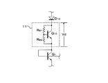
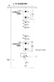
図10は、第2の実施の形態としてのLED駆動回路1の構成例を示している。この図に示すLED駆動回路1は、図9にて説明した第1の実施の形態としてのLED駆動回路において生じ得るLEDの発光輝度差を抑制できる構成を採る。なお、この図10において、図1と同一部分には同一符号を付して説明を省略する。
FIG. 10 shows a configuration example of the
この図に示すLED駆動回路1においては、トランジスタQ1とは個別とされていた電圧降下回路部11が省略されている。これに代えて、第1直列駆動回路部21においてカレントミラー回路を形成するトランジスタQ1のコレクタ−ベース間に対して抵抗Rv1を接続し、ベース− エミッタ間に対して抵抗RV2を接続することとしている。
このようにして、抵抗Rv1、抵抗RV2が接続されることに応じて、トランジスタQ1のコレクタ−ベース間には一定の電位差が生じることになる。そして、この場合のトランジスタQ1のコレクタ−エミッタ間電圧(VCE1)は、トランジスタQ1のベース−エミッタ間電圧をVBE1として、
VCE1=VBE1×(Rv1+Rv2)/Rv2・・・(式2)
により表される一定値となる。
In the
In this way, a constant potential difference is generated between the collector and base of the transistor Q1 in accordance with the connection of the resistors Rv1 and RV2. In this case, the collector-emitter voltage (VCE1) of the transistor Q1 is VBE1 as the base-emitter voltage of the transistor Q1.
VCE1 = VBE1 × (Rv1 + Rv2) / Rv2 (Formula 2)
Is a constant value represented by
ここで、トランジスタQ1のベース−エミッタ間電圧(VBE1)=0.7Vであるとして、上記式2に基づいてRv1、抵抗RV2の抵抗値を選定したことにより、コレクタ−エミッタ間電圧(VCE1)については10.7Vに設定したとする。すると、図10にも示しているように、第1直列駆動回路部21においては、トランジスタQ1のコレクタ−ベース間電圧として、10V(10.7−0.7)の電圧降下を生じているものとしてみることができる。一方の図1の場合には、トランジスタQ1のコレクタとベースが接続されている状態にあるので、コレクタ−ベース間の電位差は0であり、従って、コレクタ−エミッタ間電圧(VCE1)は、ベース−エミッタ間電圧と同じ0.7Vである。つまり、第2の実施の形態では、電圧降下回路部11を省略した代わりに、トランジスタQ1のコレクタ−ベース間電圧について、一定の電位を生じさせることで、降下電圧Vdを生じさせていることが分かる。
Here, assuming that the base-emitter voltage (VBE1) of the transistor Q1 is 0.7V, the collector-emitter voltage (VCE1) is obtained by selecting the resistance values of Rv1 and RV2 based on the
ここで、図10に示す回路においては、先の図9と同様に、LEDの電圧降下のばらつきが3.0V〜4.0Vの範囲であるものと想定したうえで、第1直列駆動回路部21におけるLED直列回路(D10〜D19)による全体の電圧降下については、ばらつき範囲の上限に対応する40V(=4.0×10)とし、第2直列駆動回路部22におけるLED直列回路(D20〜D29)による全体の電圧降下は、ばらつき範囲の下限に対応する30V(=3.0×10)であるとする。また、トランジスタQ1においては、上記したように、ベース−エミッタ間電圧VBE1=0.7V、コレクタ−エミッタ間電圧VCE1=10.7Vとする。エミッタ抵抗R11による降下電圧は0.3Vである。
この場合、第1直列駆動回路部21では、LED直列回路(D10〜D19)による40Vの電圧降下と、トランジスタQ1のコレクタ−エミッタ間電圧(VCE1)としての10.7Vの電圧降下と、エミッタ抵抗R11による0.3Vの電圧降下とが存在することになるので、第1直列駆動回路部21にかかる電圧Voとしては、
Vo=51V(=40V+10.7V+0.3V)
となる。
このときの第2直列駆動回路部22におけるトランジスタQ2のコレクタ−エミッタ間電圧(VCE2)は、
VCE2=20.7V(=51V−(30V+0.3V))
である。
このトランジスタQ2のコレクタ−エミッタ間電圧(VCE2)が20.7Vであること自体は、図9の場合とで変わらない。
Here, in the circuit shown in FIG. 10, similarly to FIG. 9, it is assumed that the variation in the voltage drop of the LED is in the range of 3.0 V to 4.0 V, and then in the first series drive circuit unit 21. The overall voltage drop due to the LED series circuit (D10 to D19) is 40V (= 4.0 × 10) corresponding to the upper limit of the variation range, and the entire LED series circuit (D20 to D29) in the second series
In this case, in the first series drive circuit section 21, a voltage drop of 40V due to the LED series circuit (D10 to D19), a voltage drop of 10.7V as the collector-emitter voltage (VCE1) of the transistor Q1, and an emitter resistance R11 Therefore, the voltage Vo applied to the first series drive circuit unit 21 is as follows:
Vo = 51V (= 40V + 10.7V + 0.3V)
It becomes.
The collector of the transistor Q2 in the second series
VCE2 = 20.7V (= 51V- (30V + 0.3V))
It is.
The fact that the collector-emitter voltage (VCE2) of the transistor Q2 is 20.7 V is not different from the case of FIG.
しかしながら、この第2の実施の形態では、トランジスタQ1のコレクタ−エミッタ間電圧(VCE1)が、10.7Vとなっている。従って、トランジスタQ1のコレクタ−エミッタ間電圧(VCE1)と、トランジスタQ2のコレクタ−エミッタ間電圧(VCE2)との差は、10Vとなる。
比較として、図9の場合には、トランジスタQ1のコレクタ−エミッタ間電圧(VCE1)は0.7Vであり、トランジスタQ2のコレクタ−エミッタ間電圧(VCE2)は、20.7Vであり、その差は、20Vとなっている。
このことから、第2の実施の形態では、例えば第1直列駆動回路部21において同じ降下電圧Vdを与えたとしても、第1の実施の形態と比較した場合には、トランジスタQ1、Q2の間でのコレクタ−エミッタ間電圧の差(|Vce1−VCE2|)が縮小されている、ということになる。
このようにして、トランジスタQ1、Q2の間でのコレクタ−エミッタ間電圧の差(|Vce1−VCE2|)が縮小されることは、トランジスタのVCE−Ic特性に基づけば、第1直列駆動回路部21におけるLED(D10〜D19)と、第2直列駆動回路部22におけるLED(D20〜D29)に流れる駆動電流量の差も小さくなるということを意味する。この結果、第1直列駆動回路部21におけるLED(D10〜D19)と、第2直列駆動回路部22におけるLED(D20〜D29)との発光輝度差も縮小されることになり、例えば光源として使用した場合の発光面の輝度ムラなども抑制される。
However, in the second embodiment, the collector-emitter voltage (VCE1) of the transistor Q1 is 10.7V. Therefore, the difference between the collector-emitter voltage (VCE1) of the transistor Q1 and the collector-emitter voltage (VCE2) of the transistor Q2 is 10V.
For comparison, in the case of FIG. 9, the collector-emitter voltage (VCE1) of the transistor Q1 is 0.7V, the collector-emitter voltage (VCE2) of the transistor Q2 is 20.7V, and the difference is 20V. It has become.
From this, in the second embodiment, for example, even if the same voltage drop Vd is given in the first series drive circuit unit 21, when compared with the first embodiment, it is between the transistors Q1 and Q2. This means that the collector-emitter voltage difference (| Vce1−VCE2 |) is reduced.
In this way, the collector-emitter voltage difference (| Vce1-VCE2 |) between the transistors Q1 and Q2 is reduced based on the VCE-Ic characteristic of the transistor. This means that the difference in the amount of drive current flowing through the LEDs (D10 to D19) in 21 and the LEDs (D20 to D29) in the second series
上記図10に示したケースは、基準となる第1直列駆動回路部21のLED直列回路の電圧
降下のばらつきが上限の40Vで、追従側の第2直列駆動回路部22のLED直列回路の電圧降下のばらつきが下限の30Vである場合を示している。逆に、第1直列駆動回路部21のLED直列回路の電圧降下のばらつきが下限の30Vで、第2直列駆動回路部22のLED直列回路の電圧降下のばらつきが上限の40Vである場合には次のようになる。
この場合、第1直列駆動回路部21では、LED直列回路(D10〜D19)による30Vの電圧降下と、トランジスタQ1のコレクタ−エミッタ間電圧(VCE1)としての10.7Vの電圧降下と、エミッタ抵抗R11による0.3Vの電圧降下とが存在することになるので、第1直列駆動回路部21にかかる電圧Voとしては、
Vo=41V(=30V+10.7V+0.3V)
となる。すると、このときの第2直列駆動回路部22におけるトランジスタQ2のコレクタ−エミッタ間電圧(VCE2)は、
VCE2=0.7V(=41V−(40V+0.3V))
となる。このときには、トランジスタQ1のコレクタ−エミッタ間電圧(VCE1)と、トランジスタQ2のコレクタ−エミッタ間電圧(VCE2)との大小関係は図10の場合と逆になるが、その差は10Vであり、図10と同じである。
The case shown in FIG. 10, at 4 0V variation in voltage drop of the upper limit of the LED series circuit of a first series drive circuit section 21 serving as the reference, following side of the LED series circuit of the second
In this case, in the first series drive circuit unit 21, a voltage drop of 30V due to the LED series circuit (D10 to D19), a voltage drop of 10.7V as the collector-emitter voltage (VCE1) of the transistor Q1, and an emitter resistance R11 Therefore, the voltage Vo applied to the first series drive circuit unit 21 is as follows:
Vo = 41V (= 30V + 10.7V + 0.3V)
It becomes. Then, the collector-emitter voltage (VCE2) of the transistor Q2 in the second series
VCE2 = 0.7V (= 41V- (40V + 0.3V))
It becomes. At this time, the magnitude relationship between the collector-emitter voltage (VCE1) of the transistor Q1 and the collector-emitter voltage (VCE2) of the transistor Q2 is opposite to that in FIG. 10, but the difference is 10V. 10 is the same.
また、第1直列駆動回路部21と第2直列駆動回路部22のLED直列回路の電圧降下のばらつきがa(V)で共に同じとなる場合には、第1直列駆動回路部21にかかる電圧Voとしては、
Vo=11+a(V)(=a+10.7V+0.3V)
となり、このときの第2直列駆動回路部22におけるトランジスタQ2のコレクタ−エミッタ間電圧(VCE2)は、
VCE2=10.7V(=11+a−(a+0.3V))
となる。つまり、このときのトランジスタQ1のコレクタ−エミッタ間電圧(VCE1)と、トランジスタQ2のコレクタ−エミッタ間電圧(VCE2)は同等となり、理論上でのLEDの発光輝度差は生じない状態となる。
このことから、第2の実施の形態では、トランジスタQ1のコレクタ−エミッタ間電圧(VCE1)を基準としたトランジスタQ2のコレクタ−エミッタ間電圧(VCE2)との差(|Vce1−VCE2|)は、±10Vの範囲での差に収まっているということがいえる。
In addition, when the variation in the voltage drop of the LED series circuit of the first series drive circuit unit 21 and the second series
Vo = 11 + a (V) (= a + 10.7V + 0.3V)
Next, the collector of the transistor Q2 in the second series
VCE2 = 10.7V (= 11 + a- (a + 0.3V))
It becomes. That is, the collector-emitter voltage (VCE1) of the transistor Q1 and the collector-emitter voltage (VCE2) of the transistor Q2 at this time are equivalent, and the theoretical LED emission luminance difference does not occur.
Therefore, in the second embodiment, the difference (| Vce1-VCE2 |) from the collector-emitter voltage (VCE2) of the transistor Q2 with respect to the collector-emitter voltage (VCE1) of the transistor Q1 is It can be said that the difference is within the range of ± 10V.
また、上記のようにして、第1直列駆動回路部21と第2直列駆動回路部22のLED直列回路の電圧降下レベルが共に同じとなる場合において、トランジスタQ1のコレクタ−エミッタ間電圧(VCE1)とトランジスタQ2のコレクタ−エミッタ間電圧(VCE2)が同等となるようにされていることによっては、次のような利点がある。
実際において、LEDを無作為に選別してLED直列回路を形成した場合における降下電圧のばらつきは、ばらつきの範囲における或る値が最も高い出現率を示し、この値から離れるほど出現率が低くなっていくという分布になると考えられる。このことは換言すれば、LED直列回路の降下電圧Vdの実際のばらつきも、上記した最も確率の高くなる値に近い範囲で生じていると考えてよい、ということである。
このことと、先に説明した第1直列駆動回路部21と第2直列駆動回路部22のLED直列回路の電圧降下レベルが共に同じであれば、トランジスタQ1,Q2のコレクタ−エミッタ間電圧(VCE1、VCE2)が同等となる、ということと照らし合わせれば、第2の実施の形態を実際に適用した光源装置としては、LEDの発光輝度差について非常に狭い範囲に抑えることができる、ということがいえる。
Further, as described above, when the voltage drop levels of the LED series circuits of the first series drive circuit unit 21 and the second series
In practice, when the LEDs are randomly selected to form an LED series circuit, the variation in the voltage drop shows the highest appearance rate at a certain value in the range of variation, and the appearance rate decreases as the distance from this value increases. It is thought that the distribution will continue. In other words, it can be considered that the actual variation of the voltage drop Vd of the LED series circuit is also generated in a range close to the above-mentioned value having the highest probability.
If this is the same as the voltage drop level of the LED series circuit of the first series drive circuit unit 21 and the second series
図11は、第2の実施の形態におけるカレントミラー回路の回路形態についての変形例を示している。なお、この図において、図10及び図8と同一とされる部位については同一符号を付し、同一内容についての説明は省略する。
この図に示す変形例は、第2の実施の形態の構成について、先に図8に示した第1の実施の形態の変形例の構成を適用したものである。つまり、カレントミラー回路を形成するためのトランジスタQ1、Q2、Q3、Q4についてPNPを選定する。そして、第1直列駆動回路部21では、トランジスタQ1のエミッタを、エミッタ抵抗R11を介して電圧Voのラインと接続し、コレクタをLED直列回路(D10〜D19)におけるアノード側端部(D10のアノード)と接続する。そのうえで、トランジスタQ1については、図10と同様にして、トランジスタQ1のコレクタ−ベース間に対して抵抗Rv1を接続し、ベース−エミッタ間に対して抵抗RV2を接続する。
第2〜第4直列駆動回路部22,23,24では、トランジスタQ2、Q3、Q4について、上記第1直列駆動回路部21と同様の態様により接続する。そのうえで、トランジスタQ1、Q2、Q3、Q4のベースを相互に接続する。
また、第1直列駆動回路部21においては、LED直列回路のカソード側の端部(D19のカソード)とアースとの間に対して、駆動電流レベルを検出するための検出抵抗Rdを挿入しており、その検出出力を定電流回路10のフィードバック端子に供給するようにしている。
このような構成によると、第1〜第4直列駆動回路部21〜24は、定電流回路10の出力である電圧Voのラインに対して並列に接続されることになる。また、第1〜第4直列駆動回路部21〜24に対して、PNPトランジスタによるカレントミラー回路が形成されることになる。
そして、このような構成であっても、第1直列駆動回路部21のトランジスタQ1のコレクタ−ベース間電圧としては降下電圧Vdに相当する電位が得られることになり、コレクタ−エミッタ間電圧(VCE1)として、ベース−エミッタ間電圧より大きい一定レベルが得られる。これにより、図10の構成と同様にして、LED直列回路の電圧降下のばらつきに対して、トランジスタQ1と、他のトランジスタQ2、Q3、Q4の間でのコレクタ−エミッタ間電圧の差について、0を基準とする正負による一定範囲内に縮小することが可能になる。
FIG. 11 shows a modification of the circuit configuration of the current mirror circuit in the second embodiment. In this figure, parts that are the same as those in FIGS. 10 and 8 are given the same reference numerals, and descriptions of the same contents are omitted.
The modification shown in this figure is obtained by applying the configuration of the modification of the first embodiment shown in FIG. 8 to the configuration of the second embodiment. That is, PNPs are selected for the transistors Q1, Q2, Q3, and Q4 for forming the current mirror circuit. In the first series drive circuit unit 21, the emitter of the transistor Q1 is connected to the voltage Vo line via the emitter resistor R11, and the collector is connected to the anode side end (the anode of D10) of the LED series circuit (D10 to D19). ). In addition, for the transistor Q1, a resistor Rv1 is connected between the collector and the base of the transistor Q1, and a resistor RV2 is connected between the base and the emitter, as in FIG.
In the second to fourth series
Further, in the first series drive circuit unit 21, a detection resistor Rd for detecting the drive current level is inserted between the cathode side end (D19 cathode) of the LED series circuit and the ground. The detection output is supplied to the feedback terminal of the constant
According to such a configuration, the first to fourth series drive circuit units 21 to 24 are connected in parallel to the line of the voltage Vo that is the output of the constant
Even with such a configuration, a potential corresponding to the drop voltage Vd is obtained as the collector-base voltage of the transistor Q1 of the first series drive circuit section 21, and the collector-emitter voltage (VCE1) is obtained. ), A constant level larger than the base-emitter voltage is obtained. Thus, in the same manner as in the configuration of FIG. 10, the difference between the collector-emitter voltage between the transistor Q1 and the other transistors Q2, Q3, Q4 is 0 with respect to the voltage drop variation of the LED series circuit. It becomes possible to reduce within a certain range by positive and negative with reference to.
ところで、トランジスタQ1のコレクタ−エミッタ間電圧(VCE1)は、先の(式2)により表されるが、実際におけるバイポーラトランジスタのベース−エミッタ間電圧は、温度特性を持っている(例えば、−2mV/C°)。このために、温度に応じて、トランジスタQ1のコレクタ−エミッタ間電圧(VCE1)は変動する。
図12は、第2の実施の形態の変形例として、上記したコレクタ−エミッタ間電圧(VCE1)の変動について温度補償を与えた構成を示している。なお、この図においては、第1直列駆動回路部21のみを示しているが、他の部位については、例えば図10と同様とされればよい。
この図において、トランジスタQ1のコレクタ−ベース間に対しては、図10の場合と同様にして抵抗Rv1のみが接続されているが、ベース−エミッタ間に対しては、次のようにして、抵抗RV21、RV22、サーミスタTHが接続される。この場合には、先ず、図10に示されている抵抗RV2を、抵抗Rv21、Rv22に分割して、この抵抗Rv21−Rv22の直列接続回路を、ベース−エミッタ間に対して接続する。この場合には、抵抗Rv21−Rv22の直列接続回路は、抵抗Rv21側の端部がベースに接続され、抵抗Rv22側の端部がエミッタ側に接続される。そして、抵抗Rv22に対してサーミスタTHが並列に接続される。なお、図10に示されるようにして、ベース−エミッタ間に接続した抵抗RV2に対してサーミスタTHを並列に接続する回路構成を採ることも考えられるが、この場合には、抵抗値の可変量などを考慮して抵抗RV2を、抵抗Rv21、Rv22に分割し、一方の抵抗R22に対してサーミスタTHを並列接続した構成としているものである。
Incidentally, the collector-emitter voltage (VCE1) of the transistor Q1 is expressed by the above (formula 2), but the actual base-emitter voltage of the bipolar transistor has a temperature characteristic (for example, -2 mV). / C °). For this reason, the collector-emitter voltage (VCE1) of the transistor Q1 varies depending on the temperature.
FIG. 12 shows, as a modification of the second embodiment, a configuration in which temperature compensation is given for the fluctuation of the collector-emitter voltage (VCE1) described above. Although only the first series drive circuit unit 21 is shown in this figure, the other parts may be the same as those shown in FIG. 10, for example.
In this figure, only the resistor Rv1 is connected between the collector and base of the transistor Q1 in the same manner as in FIG. 10, but the resistance between the base and emitter is set as follows. RV21, RV22 and the thermistor TH are connected. In this case, first, the resistor RV2 shown in FIG. 10 is divided into resistors Rv21 and Rv22, and a series connection circuit of the resistors Rv21 to Rv22 is connected between the base and the emitter. In this case, in the series connection circuit of the resistors Rv21 to Rv22, the end portion on the resistor Rv21 side is connected to the base, and the end portion on the resistor Rv22 side is connected to the emitter side. A thermistor TH is connected in parallel to the resistor Rv22. As shown in FIG. 10, it is possible to adopt a circuit configuration in which the thermistor TH is connected in parallel to the resistor RV2 connected between the base and the emitter. In this case, the variable amount of the resistance value is considered. In consideration of the above, the resistor RV2 is divided into resistors Rv21 and Rv22, and the thermistor TH is connected in parallel to one resistor R22.
ここで、回路に温度変化が生じたとすると、これに応じてサーミスタTHの抵抗値が変化する。このサーミスタTHの抵抗値の変化は、抵抗Rv22とサーミスタTHの並列回路としての抵抗値の変化となる。抵抗Rv22とサーミスタTHの並列回路は、ベース−エミッタ間において、抵抗R21と接続されているので、サーミスタTHの抵抗値の変化は、すなわち、トランジスタQ1のベース−エミッタ間に挿入した抵抗(Rv2)の抵抗値を可変していることと同じ作用を有する。このようにして、トランジスタQ1のベース−エミッタ間の抵抗値(Rv2)が変化するということは、(式2)との対応では、抵抗Rv2と抵抗Rv1との抵抗値の比が変化することに対応するものであり、この結果、トランジスタQ1のコレクタ−エミッタ間電圧(VCE1)を変化させることになる。このトランジスタQ1のコレクタ−エミッタ間電圧(VCE1)の変化により、温度特性に応じたコレクタ−エミッタ間電圧の変化をキャンセルさせることで、温度補償が実現される。 Here, if a temperature change occurs in the circuit, the resistance value of the thermistor TH changes accordingly. The change in resistance value of the thermistor TH is a change in resistance value as a parallel circuit of the resistor Rv22 and the thermistor TH. Since the parallel circuit of the resistor Rv22 and the thermistor TH is connected to the resistor R21 between the base and the emitter, the change in the resistance value of the thermistor TH, that is, the resistor (Rv2) inserted between the base and the emitter of the transistor Q1. This has the same effect as changing the resistance value of the. Thus, the change in the resistance value (Rv2) between the base and emitter of the transistor Q1 means that the ratio of the resistance values of the resistance Rv2 and the resistance Rv1 changes in correspondence with (Equation 2). As a result, the collector-emitter voltage (VCE1) of the transistor Q1 is changed. The temperature compensation is realized by canceling the change of the collector-emitter voltage according to the temperature characteristic by the change of the collector-emitter voltage (VCE1) of the transistor Q1.
図13は、これまでに説明した第1又は第2の実施の形態のLED駆動回路1を適用可能な表示装置の例として、液晶表示装置100の構成を簡略に示したものである。
この図に示す液晶表示装置100は、先ず、表示画面部に対応して、液晶表示パネル102と、この液晶表示パネル102の背面に対して設けられるバックライト部103を備える。液晶表示パネル102は、周知のようにして液晶層をガラスなどに封入していると共に、例えば半導体基板などにより所定解像度に応じた画素スイッチがマトリクス状に配置されて形成される。
バックライト部103は、この場合には実施の形態のLED直列回路1に対応して、光源として所定数(例えば40個)の白色LEDを所定の配置パターンにより二次元的に配置して構成されているもので、液晶表示パネル102の背面側から前面側に向けて白色光を照射するようにされている。
上記バックライト部103において備えられるとされるLEDは、バックライト駆動部104により電流を流すようにして駆動されることで発光する。また、この場合のバックライト駆動部104は、電源部105から供給される直流電圧Viにより動作するようになっている。
FIG. 13 schematically shows a configuration of a liquid crystal display device 100 as an example of a display device to which the
The liquid crystal display device 100 shown in this figure first includes a liquid
In this case, the
The LED provided in the
液晶表示パネル102における画素スイッチは、表示制御部101によって駆動される。表示制御部101は表示用のビデオ信号を入力し、この入力されたビデオ信号に応じて、液晶表示パネル202に対して、水平/垂直の走査駆動を行って画素スイッチのオン/オフを制御する。これにより、画素スイッチに対応する液晶層の偏向方向を変化させるように駆動が行われることで、液晶表示パネル102の背面から前面側に透過しようとする光の変調が行われることになる。この結果、液晶表示パネル102の画面上で画像が表示される。
The pixel switch in the liquid
この図13において、第1,第2の実施の形態として示したLED駆動装置1を適用した光源装置は、バックライト部103において備えられる光源としてのLED(D10〜D19、D20〜D29、D30〜D39、D40〜D49)と、このLEDを駆動するための部位であるバックライト駆動部104としての駆動回路の構成を組み合わせて成るものとみることができる。この場合のバックライト駆動部104としては、例えば定電流回路10や、カレントミラー回路を形成するトランジスタ(Q1、Q2、Q3、Q4)とその周辺の素子(エミッタ抵抗R11、及び抵抗RV1、Rv2、サーミスタTHなど(第2の実施の形態))となる。また、第1の実施の形態であれば、電圧降下回路部11としての構成が加わる。ただし、図3に示したようにして、電圧降下回路部11においてLEDを採用する場合には、これらのLEDは、物理的にはバックライト部103に含められる。
In FIG. 13, the light source device to which the
なお、本願発明としては、これまでに説明した実施の形態としての構成に限定されるものではない。
例えば、LED駆動回路を成す各直列回路において直列接続を形成するLEDの数、及び直列回路の並列接続数は、適宜変更されてよい。また、カレントミラー回路などの回路構成の細部についても、適宜変更されてよい。例えばカレントミラー用のトランジスタとしては、バイポーラトランジスタ以外にも、電界効果トランジスタなどの他の種類の増幅素子などを使用することができる。
また、実施の形態においては、LED駆動装置を液晶表示装置の光源装置として適用することを前提とし、白色LEDにより白色光を得るようにした構成を採ることとしている。
しかしながら、近年においては、例えばRGBの3原色、若しくは3原色以上 に対応する色のLEDを発光させ、その合成光により白色光を得るようにした技術も知られるようになってきている。例えば本発明は、このようにして異なる色のLEDを発光駆動するような表示装置の構成にも適用できる。さらに、液晶パネル以外であっても、光源を必要とするような表示デバイスを採用した表示装置であれば、本願発明を適用できる。
また、LEDは、液晶表示装置の光源以外にも、例えば照明などの光源としても使用されるようになってきている。本願発明は、光源を駆動する回路として適用することもできる。このような照明としての光源を考えた場合にも、LEDの色としては、多様な色とすることが考えられるもので、単一色には限定されない。
The present invention is not limited to the configuration as the embodiment described so far.
For example, the number of LEDs that form a series connection in each series circuit that forms the LED drive circuit and the number of parallel connections of the series circuit may be appropriately changed. Further, details of the circuit configuration such as the current mirror circuit may be changed as appropriate. For example, as a transistor for a current mirror, other types of amplifying elements such as a field effect transistor can be used besides a bipolar transistor.
In the embodiment, on the premise that the LED driving device is applied as a light source device of a liquid crystal display device, a configuration is adopted in which white light is obtained by a white LED.
However, in recent years, a technique has been known in which, for example, LEDs of colors corresponding to three primary colors of RGB, or more than three primary colors, emit light and white light is obtained by the combined light. For example, the present invention can also be applied to the configuration of a display device in which LEDs of different colors are driven to emit light. Furthermore, even if it is other than a liquid crystal panel, the present invention can be applied to any display device that employs a display device that requires a light source.
In addition to the light source of the liquid crystal display device, the LED has been used as a light source such as illumination. The present invention can also be applied as a circuit for driving a light source. Even when considering such a light source as illumination, the colors of the LEDs can be various colors, and are not limited to a single color.
1 LED駆動回路、10 定電流回路、11 電圧降下回路部、21 第1直列回路、22 第2直列回路、23 第3直列回路、24 第4直列回路、D10〜D19、D20〜D29、D30〜D39、D40〜D49、DL1〜DLn LED、D1〜Dn ダイオード素子、Q1、Q2、Q3、Q4、Q10 トランジスタ、RB1、RB2、Rf、Rv1、Rv2 抵抗
DESCRIPTION OF
Claims (13)
上記複数の直列駆動回路部のうちで基準となる直列駆動回路部に対して一定量の電流を出力するようにして動作し、上記複数の直列駆動回路部が上記電流の出力に対して並列に接続される定電流回路と、
上記基準となる直列駆動回路部に流れる電流を入力とし、該電流値と同じ電流を上記複数の直列駆動回路部のうち、上記基準となる直列駆動回路部以外の各直列駆動回路部に流すカレントミラー回路と、
上記基準となる直列駆動回路部の上記所定数の発光ダイオード素子の電圧降下が、上記基準となる直列駆動回路部以外の各直列駆動回路部の上記所定数と同じ数の発光ダイオードの電圧降下のいずれよりも小さい電圧降下の値のときであり、上記基準となる直列駆動回路部以外の各直列駆動回路部の上記所定数と同じ数の発光ダイオードの電圧降下のうち、もっとも大きな電圧降下の値について、前記いずれよりも小さい電圧降下の値と前記もっとも大きな電圧降下の値との差のレベルの電圧降下が生じるようにして、この基準となる直列駆動回路部を形成する発光ダイオード素子に対して直列となる関係により挿入される電圧降下発生回路と、
を備える発光ダイオード素子の駆動回路。 A plurality of series drive circuit portions formed including a predetermined number of light emitting diode elements connected in a serial relationship;
The plurality of series drive circuit units operate so as to output a constant amount of current to the reference series drive circuit unit, and the plurality of series drive circuit units are parallel to the current output. A constant current circuit to be connected;
A current that flows through the reference series drive circuit unit as an input, and a current that is the same as the current value flows through each of the plurality of series drive circuit units other than the reference series drive circuit unit. Mirror circuit,
The voltage drop of the predetermined number of light emitting diode elements in the reference series drive circuit unit is equal to the voltage drop of the same number of light emitting diodes in each series drive circuit unit other than the reference series drive circuit unit. When the voltage drop value is smaller than any of the above, the largest voltage drop value among the voltage drops of the same number of light emitting diodes as each of the series drive circuit units other than the reference series drive circuit unit. With respect to the light emitting diode elements that form the reference series drive circuit section, a voltage drop of a difference level between the value of the voltage drop smaller than any of the above and the value of the largest voltage drop occurs. A voltage drop generation circuit inserted by a serial relationship;
The drive circuit of the light emitting diode element provided with.
上記複数の直列駆動回路部のうちで基準となる直列駆動回路部に対して一定量の電流を出力するようにして動作し、上記複数の直列駆動回路部が上記電流の出力に対して並列に接続される定電流回路と、
上記基準となる直列駆動回路部に流れる電流を入力とし、該電流値と同じ電流を上記複数の直列駆動回路部のうち、上記基準となる直列駆動回路部以外の各直列駆動回路部に流すカレントミラー回路と、
上記基準となる直列駆動回路部の上記所定数の発光ダイオード素子の電圧降下が、上記基準となる直列駆動回路部以外の各直列駆動回路部の上記所定数と同じ数の発光ダイオードの電圧降下のいずれよりも小さい電圧降下の値のときであり、上記基準となる直列駆動回路部以外の各直列駆動回路部の上記所定数と同じ数の発光ダイオードの電圧降下のうち、もっとも大きな電圧降下の値について、前記いずれよりも小さい電圧降下の値と前記もっとも大きな電圧降下の値との差のレベルの電圧降下が生じるようにして、この基準となる直列駆動回路部を形成する発光ダイオード素子に対して直列となる関係により挿入される電圧降下発生回路と、
を備える光源装置。 A plurality of series drive circuit portions formed by including light emitting diode elements as a predetermined number of light sources connected in a serial relationship;
The plurality of series drive circuit units operate so as to output a constant amount of current to the reference series drive circuit unit, and the plurality of series drive circuit units are parallel to the current output. A constant current circuit to be connected;
A current that flows through the reference series drive circuit unit as an input, and a current that is the same as the current value flows through each of the plurality of series drive circuit units other than the reference series drive circuit unit. Mirror circuit,
The voltage drop of the predetermined number of light emitting diode elements in the reference series drive circuit unit is equal to the voltage drop of the same number of light emitting diodes in each series drive circuit unit other than the reference series drive circuit unit. When the voltage drop value is smaller than any of the above, the largest voltage drop value among the voltage drops of the same number of light emitting diodes as each of the series drive circuit units other than the reference series drive circuit unit. With respect to the light emitting diode elements that form the reference series drive circuit section, a voltage drop of a difference level between the value of the voltage drop smaller than any of the above and the value of the largest voltage drop occurs. A voltage drop generation circuit inserted by a serial relationship;
A light source device comprising:
上記光源装置は、
直列となる関係により接続された所定数の光源としての発光ダイオード素子を含んで形成される複数の直列駆動回路部と、
上記複数の直列駆動回路部のうちで基準となる直列駆動回路部に対して一定量の電流を出力するようにして動作し、上記複数の直列駆動回路部が上記電流の出力に対して並列に接続される定電流回路と、
上記基準となる直列駆動回路部に流れる電流を入力とし、該電流値と同じ電流を上記複数の直列駆動回路部のうち、上記基準となる直列駆動回路部以外の各直列駆動回路部に流すカレントミラー回路と、
上記基準となる直列駆動回路部の上記所定数の発光ダイオード素子の電圧降下が、上記基準となる直列駆動回路部以外の各直列駆動回路部の上記所定数と同じ数の発光ダイオードの電圧降下のいずれよりも小さい電圧降下の値のときであり、上記基準となる直列駆動回路部以外の各直列駆動回路部の上記所定数と同じ数の発光ダイオードの電圧降下のうち、もっとも大きな電圧降下の値について、前記いずれよりも小さい電圧降下の値と前記もっとも大きな電圧降下の値との差のレベルの電圧降下が生じるようにして、この基準となる直列駆動回路部を形成する発光ダイオード素子に対して直列となる関係により挿入される電圧降下発生回路とを備える表示装置。 A light source device, and an image display panel configured to display an image using light emitted from the light source device,
The light source device is
A plurality of series drive circuit portions formed by including light emitting diode elements as a predetermined number of light sources connected in a serial relationship;
The plurality of series drive circuit units operate so as to output a constant amount of current to the reference series drive circuit unit, and the plurality of series drive circuit units are parallel to the current output. A constant current circuit to be connected;
A current that flows through the reference series drive circuit unit as an input, and a current that is the same as the current value flows through each of the plurality of series drive circuit units other than the reference series drive circuit unit. Mirror circuit,
The voltage drop of the predetermined number of light emitting diode elements in the reference series drive circuit unit is equal to the voltage drop of the same number of light emitting diodes in each series drive circuit unit other than the reference series drive circuit unit. When the voltage drop value is smaller than any of the above, the largest voltage drop value among the voltage drops of the same number of light emitting diodes as each of the series drive circuit units other than the reference series drive circuit unit. With respect to the light emitting diode elements that form the reference series drive circuit section, a voltage drop of a difference level between the value of the voltage drop smaller than any of the above and the value of the largest voltage drop occurs. A display device comprising a voltage drop generation circuit inserted in a series relationship.
上記複数の直列駆動回路部のうちで基準となる直列駆動回路部に対して一定量の電流を出力するようにして動作し、上記複数の直列駆動回路部が上記電流の出力に対して並列に接続される定電流回路と、
上記基準となる直列駆動回路部に流れる電流を入力とし、該電流値と同じ電流を上記複数の直列駆動回路部のうち、上記基準となる直列駆動回路部以外の各直列駆動回路部に流すカレントミラー回路と、
上記カレントミラー回路の形成部位であり、入力端子、出力端子及び制御端子を有し、上記基準となる直列駆動回路部において上記入力端子と上記出力端子の間が直列に挿入されるカレントミラー用トランジスタ素子について、上記入力端子と上記制御端子の間および上記出力端子と上記制御端子との間にそれぞれ所定の抵抗を挿入し、上記基準となる直列駆動回路部の上記所定数の発光ダイオード素子の電圧降下が、上記基準となる直列駆動回路部以外の各直列駆動回路部の上記所定数と同じ数の発光ダイオードの電圧降下のいずれよりも小さい電圧降下の値のときであり、上記基準となる直列駆動回路部以外の各直列駆動回路部の上記所定数と同じ数の発光ダイオードの電圧降下のうち、もっとも大きな電圧降下の値について、前記いずれよりも小さい電圧降下の値と前記もっとも大きな電圧降下の値との差の電圧を生じさせるように形成される電圧発生回路と、
を備える発光ダイオード素子の駆動回路。 A plurality of series drive circuit portions formed including a predetermined number of light emitting diode elements connected in a serial relationship;
The plurality of series drive circuit units operate so as to output a constant amount of current to the reference series drive circuit unit, and the plurality of series drive circuit units are parallel to the current output. A constant current circuit to be connected;
A current that flows through the reference series drive circuit unit as an input, and a current that is the same as the current value flows through each of the plurality of series drive circuit units other than the reference series drive circuit unit. Mirror circuit,
A current mirror transistor, which is a formation part of the current mirror circuit, has an input terminal, an output terminal, and a control terminal, and is inserted in series between the input terminal and the output terminal in the reference series drive circuit unit About the element, a predetermined resistance is inserted between the input terminal and the control terminal and between the output terminal and the control terminal, respectively, and the voltage of the predetermined number of light-emitting diode elements in the reference series drive circuit unit When the drop is a voltage drop value smaller than any of the voltage drops of the same number of light-emitting diodes as the predetermined number of each of the series drive circuit units other than the reference series drive circuit unit, the reference series Among the voltage drops of the same number of light emitting diodes as the above-mentioned predetermined number in each series drive circuit part other than the drive circuit part, the value of the largest voltage drop is A voltage generating circuit which is formed to produce a voltage difference between the value and the value of the largest voltage drop smaller voltage drop than,
The drive circuit of the light emitting diode element provided with.
上記複数の直列駆動回路部のうちで基準となる直列駆動回路部に対して一定量の電流を出力するようにして動作し、上記複数の直列駆動回路部が上記電流の出力に対して並列に接続される定電流回路と、
上記基準となる直列駆動回路部に流れる電流を入力とし、該電流値と同じ電流を上記複数の直列駆動回路部のうち、上記基準となる直列駆動回路部以外の各直列駆動回路部に流すカレントミラー回路と、
上記カレントミラー回路の形成部位であり、入力端子、出力端子及び制御端子を有し、上記基準となる直列駆動回路部において上記入力端子と上記出力端子の間が直列に挿入されるカレントミラー用トランジスタ素子について、上記入力端子と上記制御端子の間および上記出力端子と上記制御端子との間にそれぞれ所定の抵抗を挿入し、上記基準となる直列駆動回路部の上記所定数の発光ダイオード素子の電圧降下が、上記基準となる直列駆動回路部以外の各直列駆動回路部の上記所定数と同じ数の発光ダイオードの電圧降下のいずれよりも小さい電圧降下の値のときであり、上記基準となる直列駆動回路部以外の各直列駆動回路部の上記所定数と同じ数の発光ダイオードの電圧降下のうち、もっとも大きな電圧降下の値について、前記いずれよりも小さい電圧降下の値と前記もっとも大きな電圧降下の値との差の電圧を生じさせるように形成される電圧発生回路と、
を備える光源装置。 A plurality of series drive circuit portions formed by including light emitting diode elements as a predetermined number of light sources connected in a serial relationship;
The plurality of series drive circuit units operate so as to output a constant amount of current to the reference series drive circuit unit, and the plurality of series drive circuit units are parallel to the current output. A constant current circuit to be connected;
A current that flows through the reference series drive circuit unit as an input, and a current that is the same as the current value flows through each of the plurality of series drive circuit units other than the reference series drive circuit unit. Mirror circuit,
A current mirror transistor, which is a formation part of the current mirror circuit, has an input terminal, an output terminal, and a control terminal, and is inserted in series between the input terminal and the output terminal in the reference series drive circuit unit About the element, a predetermined resistance is inserted between the input terminal and the control terminal and between the output terminal and the control terminal, respectively, and the voltage of the predetermined number of light-emitting diode elements in the reference series drive circuit unit When the drop is a voltage drop value smaller than any of the voltage drops of the same number of light-emitting diodes as the predetermined number of each of the series drive circuit units other than the reference series drive circuit unit, the reference series Among the voltage drops of the same number of light emitting diodes as the above-mentioned predetermined number in each series drive circuit part other than the drive circuit part, the value of the largest voltage drop is A voltage generating circuit which is formed to produce a voltage difference between the value and the value of the largest voltage drop smaller voltage drop than,
A light source device comprising:
上記光源装置は、
直列となる関係により接続された所定数の光源としての発光ダイオード素子を含んで形成される複数の直列駆動回路部と、
上記複数の直列駆動回路部のうちで基準となる直列駆動回路部に対して一定量の電流を出力するようにして動作し、上記複数の直列駆動回路部が上記電流の出力に対して並列に接続される定電流回路と、
上記基準となる直列駆動回路部に流れる電流を入力とし、該電流値と同じ電流を上記複数の直列駆動回路部のうち、上記基準となる直列駆動回路部以外の各直列駆動回路部に流すカレントミラー回路と、
上記カレントミラー回路の形成部位であり、入力端子、出力端子及び制御端子を有し、上記基準となる直列駆動回路部において上記入力端子と上記出力端子の間が直列に挿入されるカレントミラー用トランジスタ素子について、上記入力端子と上記制御端子の間および上記出力端子と上記制御端子との間にそれぞれ所定の抵抗を挿入し、上記基準となる直列駆動回路部の上記所定数の発光ダイオード素子の電圧降下が、上記基準となる直列駆動回路部以外の各直列駆動回路部の上記所定数と同じ数の発光ダイオードの電圧降下のいずれよりも小さい電圧降下の値のときであり、上記基準となる直列駆動回路部以外の各直列駆動回路部の上記所定数と同じ数の発光ダイオードの電圧降下のうち、もっとも大きな電圧降下の値について、前記いずれよりも小さい電圧降下の値と前記もっとも大きな電圧降下の値との差の電圧を生じさせるように形成される電圧発生回路と、
を備える表示装置。 A light source device, and an image display panel configured to display an image using light emitted from the light source device,
The light source device is
A plurality of series drive circuit portions formed by including light emitting diode elements as a predetermined number of light sources connected in a serial relationship;
The plurality of series drive circuit units operate so as to output a constant amount of current to the reference series drive circuit unit, and the plurality of series drive circuit units are parallel to the current output. A constant current circuit to be connected;
A current that flows through the reference series drive circuit unit as an input, and a current that is the same as the current value flows through each of the plurality of series drive circuit units other than the reference series drive circuit unit. Mirror circuit,
A current mirror transistor, which is a formation part of the current mirror circuit, has an input terminal, an output terminal, and a control terminal, and is inserted in series between the input terminal and the output terminal in the reference series drive circuit unit About the element, a predetermined resistance is inserted between the input terminal and the control terminal and between the output terminal and the control terminal, respectively, and the voltage of the predetermined number of light-emitting diode elements in the reference series drive circuit unit When the drop is a voltage drop value smaller than any of the voltage drops of the same number of light-emitting diodes as the predetermined number of each of the series drive circuit units other than the reference series drive circuit unit, the reference series Among the voltage drops of the same number of light emitting diodes as the above-mentioned predetermined number in each series drive circuit part other than the drive circuit part, the value of the largest voltage drop is A voltage generating circuit which is formed to produce a voltage difference between the value and the value of the largest voltage drop smaller voltage drop than,
Viewing apparatus comprising a.
Priority Applications (2)
| Application Number | Priority Date | Filing Date | Title |
|---|---|---|---|
| JP2005205761A JP4544068B2 (en) | 2005-07-14 | 2005-07-14 | Light emitting diode element drive circuit, light source device, display device |
| US11/456,434 US7864142B2 (en) | 2005-07-14 | 2006-07-10 | Light-emitting diode drive circuit, light source device, and display device |
Applications Claiming Priority (1)
| Application Number | Priority Date | Filing Date | Title |
|---|---|---|---|
| JP2005205761A JP4544068B2 (en) | 2005-07-14 | 2005-07-14 | Light emitting diode element drive circuit, light source device, display device |
Publications (2)
| Publication Number | Publication Date |
|---|---|
| JP2007027316A JP2007027316A (en) | 2007-02-01 |
| JP4544068B2 true JP4544068B2 (en) | 2010-09-15 |
Family
ID=37661212
Family Applications (1)
| Application Number | Title | Priority Date | Filing Date |
|---|---|---|---|
| JP2005205761A Expired - Fee Related JP4544068B2 (en) | 2005-07-14 | 2005-07-14 | Light emitting diode element drive circuit, light source device, display device |
Country Status (2)
| Country | Link |
|---|---|
| US (1) | US7864142B2 (en) |
| JP (1) | JP4544068B2 (en) |
Families Citing this family (40)
| Publication number | Priority date | Publication date | Assignee | Title |
|---|---|---|---|---|
| US20070152909A1 (en) * | 2006-01-05 | 2007-07-05 | Sanyo Electric Co., Ltd. | Led device |
| KR101254595B1 (en) * | 2006-09-12 | 2013-04-16 | 엘지디스플레이 주식회사 | Apparatus for driving of back light |
| KR101255268B1 (en) * | 2006-09-12 | 2013-04-15 | 엘지디스플레이 주식회사 | Back light unit and liquid crystal display device using the same |
| US8324816B2 (en) * | 2006-10-18 | 2012-12-04 | Koa Corporation | LED driving circuit |
| EP2094063A4 (en) * | 2006-10-25 | 2010-12-01 | Panasonic Elec Works Co Ltd | Led lighting circuit and illuminating apparatus using the same |
| US7683553B2 (en) * | 2007-05-01 | 2010-03-23 | Pacifictech Microelectronics, Inc. | LED current control circuits and methods |
| JP4577525B2 (en) | 2007-05-31 | 2010-11-10 | 東芝ライテック株式会社 | Lighting device |
| JP5121318B2 (en) * | 2007-06-12 | 2013-01-16 | 三菱電機株式会社 | Power supply device, light emitting diode lighting device and guide lamp device |
| KR20100021518A (en) * | 2007-06-13 | 2010-02-24 | 오스람 게젤샤프트 미트 베쉬랭크터 하프퉁 | Circuit arrangement and actuation method for semi-conductor light sources |
| CN101816032B (en) * | 2007-09-28 | 2012-12-05 | 松下电器产业株式会社 | Light-emitting element circuit and active matrix type display device |
| US8277092B2 (en) | 2007-10-12 | 2012-10-02 | Truck-Lite Co., Llc | Lamp assembly utilizing light emitting diodes |
| JP5344809B2 (en) * | 2007-11-21 | 2013-11-20 | アルパイン株式会社 | Backlight device |
| CN101794559B (en) * | 2009-02-03 | 2013-03-20 | 乐金显示有限公司 | Backlight assembly of liquid crystal display device |
| US20100295472A1 (en) * | 2009-05-06 | 2010-11-25 | Polar Semiconductor, Inc. | Power supply for floating loads |
| US8564155B2 (en) | 2009-05-06 | 2013-10-22 | Polar Semiconductor, Inc. | Multiple output power supply |
| JP2010267481A (en) | 2009-05-14 | 2010-11-25 | Hitachi Displays Ltd | Backlight device and display device |
| US8890419B2 (en) * | 2009-05-28 | 2014-11-18 | Q Technology, Inc. | System and method providing LED emulation of incandescent bulb brightness and color response to varying power input and dimmer circuit therefor |
| US9713211B2 (en) * | 2009-09-24 | 2017-07-18 | Cree, Inc. | Solid state lighting apparatus with controllable bypass circuits and methods of operation thereof |
| US10264637B2 (en) * | 2009-09-24 | 2019-04-16 | Cree, Inc. | Solid state lighting apparatus with compensation bypass circuits and methods of operation thereof |
| US8901845B2 (en) | 2009-09-24 | 2014-12-02 | Cree, Inc. | Temperature responsive control for lighting apparatus including light emitting devices providing different chromaticities and related methods |
| JP5608394B2 (en) * | 2010-03-09 | 2014-10-15 | 株式会社ジャパンディスプレイ | Liquid crystal display |
| JP2011258797A (en) * | 2010-06-10 | 2011-12-22 | Fujitsu Semiconductor Ltd | Drive control circuit of light-emitting diode and backlight system |
| CN101923832B (en) * | 2010-07-30 | 2012-05-30 | 深圳市华星光电技术有限公司 | Backlight module |
| US8653738B2 (en) | 2010-07-30 | 2014-02-18 | Shenzhen China Star Optoelectronics Technology Co. Ltd. | Backlight module |
| KR101741742B1 (en) | 2010-09-14 | 2017-05-31 | 삼성디스플레이 주식회사 | Method of driving a light source, light source apparatus performing the method and display apparatus having the light source apparatus |
| KR20120030742A (en) | 2010-09-20 | 2012-03-29 | 삼성전자주식회사 | Display apparatus and power circuit apparatus thereof |
| US8569974B2 (en) | 2010-11-01 | 2013-10-29 | Cree, Inc. | Systems and methods for controlling solid state lighting devices and lighting apparatus incorporating such systems and/or methods |
| US8742671B2 (en) | 2011-07-28 | 2014-06-03 | Cree, Inc. | Solid state lighting apparatus and methods using integrated driver circuitry |
| KR101273384B1 (en) | 2011-09-15 | 2013-06-11 | (주)포인트텍 | Apparatus for driving multi-channel light emitting diode |
| WO2013039324A2 (en) * | 2011-09-15 | 2013-03-21 | (주)포인트텍 | Device for driving multi-channel light-emitting diode |
| US8823285B2 (en) | 2011-12-12 | 2014-09-02 | Cree, Inc. | Lighting devices including boost converters to control chromaticity and/or brightness and related methods |
| US8847516B2 (en) * | 2011-12-12 | 2014-09-30 | Cree, Inc. | Lighting devices including current shunting responsive to LED nodes and related methods |
| US9374858B2 (en) | 2012-05-21 | 2016-06-21 | Cree, Inc. | Solid-state lighting apparatus and methods using switched energy storage |
| US9119258B2 (en) * | 2013-03-06 | 2015-08-25 | General Electric Company | Current split circuit for equally splitting current between parallel connected LED luminaire strings |
| US9504103B2 (en) | 2013-10-21 | 2016-11-22 | Osram Sylvania Inc. | Driving a multi-color luminaire |
| CN103632635B (en) * | 2013-11-08 | 2016-04-13 | 电子科技大学 | Power tube grouping hybrid driving circuit |
| EP2922368B1 (en) * | 2014-03-18 | 2019-05-22 | Goodrich Lighting Systems GmbH | Multi-color interior aircraft light unit and passenger transport vehicle comprising the same |
| JPWO2016132475A1 (en) * | 2015-02-18 | 2017-04-27 | 三菱電機株式会社 | LIGHT EMITTING DEVICE AND LIGHT EMITTING DEVICE PARAMETER SETTING METHOD |
| CN107637181B (en) * | 2015-05-08 | 2020-09-15 | 昕诺飞控股有限公司 | LED lamp strip and manufacturing method thereof |
| KR102543092B1 (en) * | 2022-11-10 | 2023-06-14 | 주식회사 그린누리텍 | Led drive circuit for parallel operation |
Citations (6)
| Publication number | Priority date | Publication date | Assignee | Title |
|---|---|---|---|---|
| JP2002008409A (en) * | 2000-06-19 | 2002-01-11 | Toshiba Lighting & Technology Corp | Led light source device |
| JP2003100472A (en) * | 2001-07-19 | 2003-04-04 | Denso Corp | Driving equipment for light emitting diode |
| JP2004039684A (en) * | 2002-06-28 | 2004-02-05 | Matsushita Electric Works Ltd | Lighting device |
| JP2004134580A (en) * | 2002-10-10 | 2004-04-30 | Denso Corp | Driving circuit for light emitting diode |
| JP2004253804A (en) * | 2003-02-20 | 2004-09-09 | Visteon Global Technologies Inc | Method and device for controlling light emitting diode |
| JP2004319583A (en) * | 2003-04-11 | 2004-11-11 | Toritsu Tsushin Kogyo Kk | Led lighting system |
Family Cites Families (2)
| Publication number | Priority date | Publication date | Assignee | Title |
|---|---|---|---|---|
| JP3428029B2 (en) * | 1998-02-23 | 2003-07-22 | セイコーエプソン株式会社 | Electro-optical device driving method, electro-optical device driving circuit, electro-optical device, and electronic apparatus |
| JP2004039290A (en) | 2002-06-28 | 2004-02-05 | Matsushita Electric Works Ltd | Lighting device |
-
2005
- 2005-07-14 JP JP2005205761A patent/JP4544068B2/en not_active Expired - Fee Related
-
2006
- 2006-07-10 US US11/456,434 patent/US7864142B2/en not_active Expired - Fee Related
Patent Citations (6)
| Publication number | Priority date | Publication date | Assignee | Title |
|---|---|---|---|---|
| JP2002008409A (en) * | 2000-06-19 | 2002-01-11 | Toshiba Lighting & Technology Corp | Led light source device |
| JP2003100472A (en) * | 2001-07-19 | 2003-04-04 | Denso Corp | Driving equipment for light emitting diode |
| JP2004039684A (en) * | 2002-06-28 | 2004-02-05 | Matsushita Electric Works Ltd | Lighting device |
| JP2004134580A (en) * | 2002-10-10 | 2004-04-30 | Denso Corp | Driving circuit for light emitting diode |
| JP2004253804A (en) * | 2003-02-20 | 2004-09-09 | Visteon Global Technologies Inc | Method and device for controlling light emitting diode |
| JP2004319583A (en) * | 2003-04-11 | 2004-11-11 | Toritsu Tsushin Kogyo Kk | Led lighting system |
Also Published As
| Publication number | Publication date |
|---|---|
| JP2007027316A (en) | 2007-02-01 |
| US20070013620A1 (en) | 2007-01-18 |
| US7864142B2 (en) | 2011-01-04 |
Similar Documents
| Publication | Publication Date | Title |
|---|---|---|
| JP4544068B2 (en) | Light emitting diode element drive circuit, light source device, display device | |
| KR101493492B1 (en) | Backlight unit, liquid crystal display including the same and driving method thereof | |
| KR100512833B1 (en) | Self-luminous type display device | |
| KR101365345B1 (en) | Drive device for light emitting diode element, light source device, and display | |
| US7425728B2 (en) | Surface light source control device | |
| CN110718195B (en) | Light emitting device, display device, and LED display device | |
| KR20090093859A (en) | Drive circuit of display panel and display apparatus | |
| US20060176253A1 (en) | Driving apparatus and driving method of light emitting display panel | |
| US20040239654A1 (en) | Drive circuit for light emitting elements | |
| US7719494B2 (en) | Brightness adjustment circuit and electroluminescent display using the same | |
| JP2009054566A (en) | Light source device | |
| CN110544459B (en) | Pixel circuit, driving method thereof and display device | |
| JP2006284859A (en) | Drive method for light emission display panel | |
| WO2012081222A1 (en) | Power supply circuit and display device using same | |
| JP2013047735A (en) | Display device | |
| CN210429264U (en) | Miniature display device | |
| JP2019047095A (en) | Light-emitting element driving device, semiconductor device, light-emitting device, and liquid crystal display device | |
| JP4245495B2 (en) | Rear light source for display device and display device | |
| KR20140120168A (en) | Organic light emitting display and method for operating the same | |
| KR20120019309A (en) | Led driving apparatus | |
| TWI834387B (en) | Driving circuit for led panel and led panel thereof | |
| US20240008152A1 (en) | Light emitting diode driving circuit and backlight apparatus of display | |
| JP4800648B2 (en) | Constant current drive circuit | |
| JP2004302273A (en) | Display device, and method for driving display panel | |
| JP3164657U (en) | Display device |
Legal Events
| Date | Code | Title | Description |
|---|---|---|---|
| A521 | Written amendment |
Free format text: JAPANESE INTERMEDIATE CODE: A523 Effective date: 20061122 |
|
| A621 | Written request for application examination |
Free format text: JAPANESE INTERMEDIATE CODE: A621 Effective date: 20061122 |
|
| A977 | Report on retrieval |
Free format text: JAPANESE INTERMEDIATE CODE: A971007 Effective date: 20090707 |
|
| A131 | Notification of reasons for refusal |
Free format text: JAPANESE INTERMEDIATE CODE: A131 Effective date: 20100112 |
|
| A521 | Written amendment |
Free format text: JAPANESE INTERMEDIATE CODE: A523 Effective date: 20100305 |
|
| A131 | Notification of reasons for refusal |
Free format text: JAPANESE INTERMEDIATE CODE: A131 Effective date: 20100406 |
|
| A521 | Written amendment |
Free format text: JAPANESE INTERMEDIATE CODE: A523 Effective date: 20100521 |
|
| TRDD | Decision of grant or rejection written | ||
| A01 | Written decision to grant a patent or to grant a registration (utility model) |
Free format text: JAPANESE INTERMEDIATE CODE: A01 Effective date: 20100608 |
|
| A01 | Written decision to grant a patent or to grant a registration (utility model) |
Free format text: JAPANESE INTERMEDIATE CODE: A01 |
|
| A61 | First payment of annual fees (during grant procedure) |
Free format text: JAPANESE INTERMEDIATE CODE: A61 Effective date: 20100621 |
|
| FPAY | Renewal fee payment (event date is renewal date of database) |
Free format text: PAYMENT UNTIL: 20130709 Year of fee payment: 3 |
|
| FPAY | Renewal fee payment (event date is renewal date of database) |
Free format text: PAYMENT UNTIL: 20130709 Year of fee payment: 3 |
|
| LAPS | Cancellation because of no payment of annual fees |