JP5344809B2 - Backlight device - Google Patents
Backlight device Download PDFInfo
- Publication number
- JP5344809B2 JP5344809B2 JP2007301139A JP2007301139A JP5344809B2 JP 5344809 B2 JP5344809 B2 JP 5344809B2 JP 2007301139 A JP2007301139 A JP 2007301139A JP 2007301139 A JP2007301139 A JP 2007301139A JP 5344809 B2 JP5344809 B2 JP 5344809B2
- Authority
- JP
- Japan
- Prior art keywords
- light emitting
- emitting elements
- leds
- light
- backlight device
- Prior art date
- Legal status (The legal status is an assumption and is not a legal conclusion. Google has not performed a legal analysis and makes no representation as to the accuracy of the status listed.)
- Expired - Fee Related
Links
- 239000004973 liquid crystal related substance Substances 0.000 claims description 27
- 239000011159 matrix material Substances 0.000 claims description 27
- 238000010586 diagram Methods 0.000 description 15
- 238000000034 method Methods 0.000 description 5
- 239000000758 substrate Substances 0.000 description 2
- RYGMFSIKBFXOCR-UHFFFAOYSA-N Copper Chemical compound [Cu] RYGMFSIKBFXOCR-UHFFFAOYSA-N 0.000 description 1
- NIXOWILDQLNWCW-UHFFFAOYSA-N acrylic acid group Chemical group C(C=C)(=O)O NIXOWILDQLNWCW-UHFFFAOYSA-N 0.000 description 1
- 239000011889 copper foil Substances 0.000 description 1
- 238000009792 diffusion process Methods 0.000 description 1
- 239000003822 epoxy resin Substances 0.000 description 1
- 238000007689 inspection Methods 0.000 description 1
- 238000004519 manufacturing process Methods 0.000 description 1
- QSHDDOUJBYECFT-UHFFFAOYSA-N mercury Chemical compound [Hg] QSHDDOUJBYECFT-UHFFFAOYSA-N 0.000 description 1
- 229910052753 mercury Inorganic materials 0.000 description 1
- 238000012986 modification Methods 0.000 description 1
- 230000004048 modification Effects 0.000 description 1
- 230000003287 optical effect Effects 0.000 description 1
- 229920000647 polyepoxide Polymers 0.000 description 1
- 238000002834 transmittance Methods 0.000 description 1
Images


Landscapes
- Liquid Crystal (AREA)
- Planar Illumination Modules (AREA)
- Circuit Arrangement For Electric Light Sources In General (AREA)
Description
本発明は、液晶表示パネルの光源となるバックライト装置に関し、特に、バックライト装置の発光素子をマトリックス駆動する方式に関する。 The present invention relates to a backlight device serving as a light source of a liquid crystal display panel, and more particularly to a method of driving a light emitting element of a backlight device in a matrix manner.
液晶表示パネルは、それ自体は発光素子ではないため、その背面にバックライト装置を取り付けることが望ましい。バックライト装置には、従来より冷陰極蛍光ランプ(以下、CCFLと称する)が使用されてきたが、最近ではそれに代わって低消費電力、高寿命の発光ダイオード(light emitting diode、以下、LEDと称する)の使用が増えている。 Since the liquid crystal display panel itself is not a light emitting element, it is desirable to attach a backlight device to the back surface thereof. Conventionally, a cold cathode fluorescent lamp (hereinafter referred to as CCFL) has been used for the backlight device, but recently, a low power consumption and long-life light emitting diode (hereinafter referred to as LED) has been used instead. ) Is increasing.
CCFLは、一般的な蛍光灯と似た細長い円筒状をした線光源であり、その細長い形状を活かして導光板と組み合わされ、液晶表示パネルの光源として広く使われてきた。しかし、CCFLは、スイッチのオン/オフの繰り返しに弱く、さらに使用期間が長くなると黒ずみがでてくる、低温での特性が良くない、また、水銀を含有している、という欠点がある。そこで、新たな光源としてLEDが使用されている。LEDは、点光源であるため、バックライト光源として使用するには複数のLEDが必要となる。 The CCFL is a linear light source having an elongated cylindrical shape similar to a general fluorescent lamp, and has been widely used as a light source for a liquid crystal display panel in combination with a light guide plate utilizing the elongated shape. However, CCFLs are vulnerable to repeated ON / OFF of the switch, have darkness as they are used for a longer period of time, have poor properties at low temperatures, and contain mercury. Therefore, an LED is used as a new light source. Since the LED is a point light source, a plurality of LEDs are required for use as a backlight light source.
複数のLEDの点灯方法には、マトリックス駆動方式と直列駆動方式がある。図1(a)は4行×3列のマトリックス駆動回路の例であり、図1(b)は直列駆動回路の例である。マトリックス駆動回路は、光源駆動回路4に接続されたアノード側の共通の電源ライン3と、定電流制御のために光源駆動回路4に個別に接続されるカソード側の電源ライン6a、6b、6cとの間に並列に接続された複数の電流経路2を含む。電流経路2は、直列に接続された複数のLED1から構成されている。本明細書では、LEDのマトリックス配列に関して、電流経路2を並列に接続する方向を「行」、LED1を直列に接続する方向を「列」と呼ぶ。図1(a)は、4行×3列のマトリックス配列であるが、これ以外にも、3行×4列、6行×2列、または2行×6列であってもよい。
There are a matrix driving method and a serial driving method for lighting a plurality of LEDs. FIG. 1A is an example of a 4 × 3 matrix drive circuit, and FIG. 1B is an example of a series drive circuit. The matrix drive circuit includes a common anode-side
直列駆動回路は、図1(b)に示すように、光源駆動回路4に接続された電源ライン3に12個の全てのLEDを直列に並べただけの単純な回路である。直列駆動回路では、LEDの数に比例して駆動電圧が大きくなり、しかも、LEDを接続する配線の一部が断線すると回路全体が遮断され、液晶表示パネルへの光源が全て失われてしまうというデメリットがある。このため、中型から大型の液晶表示パネルのバックライトにLEDを用いるときには、マトリックス駆動方式を採用するのが一般的である。
As shown in FIG. 1B, the series drive circuit is a simple circuit in which all twelve LEDs are arranged in series on the
LEDは、光度にバラツキがあるため、そのバラツキ具合に応じてLEDを複数のランクに分類している。LEDの面内光度分布のバラツキを抑制したい場合には、同一光度ランクのLEDを用いれば、そのバラツキが最小化される。他方、同一光度ランクのLEDを選別することは、結果的にコスト高になってしまう。 Since LEDs have variations in luminous intensity, the LEDs are classified into a plurality of ranks according to the variations. When it is desired to suppress variations in the in-plane luminous intensity distribution of the LEDs, the variation is minimized by using LEDs having the same luminous intensity rank. On the other hand, selecting LEDs having the same luminous intensity rank results in high costs.
特許文献1は、こうした不具合を解消するため、LEDが同数ずつ含まれるように区切った各小ブロックに対して、少なくとも2つの異なるランクに分類されたLEDを搭載し、各小ブロックに搭載するLEDのランクの組合せを一致させている。
In
従来のカーナビゲーション装置では、図2(a)に示すように、例えば7インチワイド液晶表示パネルを用い、その長手方向に12個のLEDを直線状に配列している。LEDの必要数は、ディスプレイに要求される輝度、液晶の透過率、カラーフィルターの濃度、光学部材の損失、輝度上昇部材などの係数により算出される。LEDを配置する間隔を等間隔とする場合、その間隔Dは、次式で表される。 In the conventional car navigation apparatus, as shown in FIG. 2A, for example, a 7-inch wide liquid crystal display panel is used, and 12 LEDs are linearly arranged in the longitudinal direction. The required number of LEDs is calculated based on factors required for the display, such as luminance, liquid crystal transmittance, color filter density, loss of optical members, and luminance increasing members. When the intervals at which the LEDs are arranged are equally spaced, the interval D is expressed by the following equation.
7インチワイドの液晶表示パネルの有効表示エリアの長辺の長さLは約160mmであり、LEDの灯数が12であれば、LEDは、12.3mmの間隔Dで配置され、左右のLEDは、エッジから間隔Dの半分の距離6.15mmで配置される。 If the length L of the long side of the effective display area of the 7-inch wide liquid crystal display panel is about 160 mm, and the number of LEDs is 12, the LEDs are arranged at a distance D of 12.3 mm, and the left and right LEDs are , Arranged at a distance of 6.15 mm, which is half the distance D from the edge.
LEDは、上記したように光量のバラツキ以外にも、色調や順方向降下電圧(以下、VFと略す)のバラツキがあり、色調やVFに応じてLEDがランク分けされている。LEDの光量は駆動電流に比例するため、マトリックス駆動回路の各列には等しい駆動電流を流さなければならないという制約がある。このため、各列のLEDはすべて同一のVFランクにするか、あるいは各列のVFランクの組合せを等しくする必要がある。 As described above, LEDs have variations in color tone and forward voltage drop (hereinafter abbreviated as VF) in addition to variations in light quantity, and LEDs are ranked according to color tone and VF. Since the light quantity of the LED is proportional to the drive current, there is a restriction that an equal drive current must be supplied to each column of the matrix drive circuit. For this reason, all the LEDs in each column need to have the same VF rank, or the combinations of VF ranks in each column need to be equal.
図3は、12灯数のLEDのVFランクの組合せを一致させたマトリックス駆動回路を示している。同図に示すように、1行目のLEDは、VFランク(A)の3.0V、2行目のLEDは、VFランク(B)の3.4V、3行目のLEDは、VFランクVF(C)の3.8V、4行目のLEDは、VFランクVF(D)の4.2Vとし、各列の合計のVFの値が14.4Vと等しくしている。 FIG. 3 shows a matrix drive circuit in which the combinations of the VF ranks of 12 LEDs are matched. As shown in the figure, the LED in the first row is VF rank (A) 3.0V, the LED in the second row is 3.4V in VF rank (B), and the LED in the third row is VF rank. The VF (C) 3.8V and the LEDs in the fourth row are set to VF rank VF (D) 4.2V, and the total VF value of each column is equal to 14.4V.
ところで、LEDの発光効率は、技術開発等により向上しており、以前よりも少ないLEDの灯数で等価な輝度を出力することが可能である。また、使用している擬似白色LEDは、単価、ランク等の選別料、実装費、検査費などを含んでおり、これがバックライト装置や液晶表示装置のコストに反映されてしまう。このため、可能な限りLEDの灯数を削減することが望まれる。 By the way, the luminous efficiency of the LED has been improved by technological development and the like, and it is possible to output an equivalent luminance with a smaller number of LEDs than before. Moreover, the pseudo white LED used includes a sorting fee such as a unit price and a rank, a mounting cost, an inspection cost, and the like, which are reflected in the cost of the backlight device and the liquid crystal display device. For this reason, it is desired to reduce the number of LEDs as much as possible.
従来のマトリックス駆動方式によりLEDの灯数を12個から削減しようとする場合、各列の駆動電流を等しくするためLEDの灯数は10になる。LEDが10灯の場合、上記式(1)からLEDの間隔Dは、14.5mmとなり(図2(b)を参照)、LED12灯数の場合と比較して、14.5−12.3=2.2mmだけ間隔が広がってしまう。このように灯数が一気に2個削減されてしまうと、面内均一度が悪化し、液晶パネル上に光源斑が強く現れてしまう。 When the number of LED lamps is reduced from 12 by the conventional matrix drive system, the number of LED lamps is 10 in order to equalize the drive current of each column. When the number of LEDs is 10, the distance D between the LEDs is 14.5 mm from the above formula (1) (see FIG. 2B), which is 14.5-12.3 compared to the case of 12 LEDs. = The distance is increased by 2.2 mm. If the number of lamps is reduced at a stroke in this way, the in-plane uniformity is deteriorated and light source spots appear strongly on the liquid crystal panel.
他方、LEDの灯数を1つ削減し11灯数にすることも可能であるが、この場合には、図4に示すように、4行×2列のマトリックスを駆動するための光源駆動回路4と、直列接続された3つのLEDを駆動するための光源駆動回路4aを別途持たなければならず、回路が煩雑となり、その分だけ余分なコストが生じてしまう。
On the other hand, it is possible to reduce the number of LEDs by 1 to 11 but in this case, as shown in FIG. 4, a light source driving circuit for driving a matrix of 4 rows × 2 columns. 4 and a light
本発明は、このような従来の課題に着目し、コスト増加を抑制しつつ所望の数の発光素子をマトリックス駆動することができるバックライト装置を提供することを目的とする。 An object of the present invention is to provide a backlight device that can drive a desired number of light-emitting elements in a matrix while suppressing an increase in cost while paying attention to such a conventional problem.
本発明に係るバックライト装置は、第1の電源ラインと、第2の電源ラインと、第1および第2の電源ライン間に並列に接続された複数の電流経路とを含み、前記複数の電流経路の各々は、直列に接続された複数の発光素子を含み、前記複数の電流経路に含まれる第1の電流経路は第1の数の発光素子を含み、前記複数の電流経路に含まれる第2の電流経路は第1の数と異なる第2の数の発光素子を含み、第1の電流経路に含まれる発光素子の順方向降下電圧の合計と第2の電流経路に含まれる発光素子の順方向降下電圧の差分は一定値以内にある。 The backlight device according to the present invention includes a first power line, a second power line, and a plurality of current paths connected in parallel between the first and second power lines, and the plurality of currents Each of the paths includes a plurality of light emitting elements connected in series, and the first current path included in the plurality of current paths includes a first number of light emitting elements and is included in the plurality of current paths. The second current path includes a second number of light emitting elements different from the first number, and the total of forward drop voltages of the light emitting elements included in the first current path and the light emitting elements included in the second current path. The difference in forward voltage drop is within a certain value.
好ましくは、第1の電流経路に含まれる発光素子の順方向降下電圧の組合せは、第2の電流経路に含まれる発光素子の順方向降下電圧の組合せと異なる。好ましくは、第1および第2の電流経路に含まれる各発光素子は、光度に基づき分類された光度ランクと色調に基づき分類された色調ランクが同一である。好ましくは、前記複数の電流経路に含まれる各発光素子は、基板上に等間隔で直線状に配置されている。好ましくは、バックライト装置はさらに、発光素子からの光を拡散する導光板を含む。 Preferably, the combination of the forward drop voltages of the light emitting elements included in the first current path is different from the combination of the forward drop voltages of the light emitting elements included in the second current path. Preferably, each light emitting element included in the first and second current paths has the same light intensity rank classified based on light intensity and the same color rank classified based on color tone. Preferably, the light emitting elements included in the plurality of current paths are linearly arranged on the substrate at equal intervals. Preferably, the backlight device further includes a light guide plate that diffuses light from the light emitting element.
本発明によれば、第1および第2の電流経路に含まれる発光素子の数が異なるとき、それらの順方向降下電圧の合計を一定値以内にすることで、光源駆動回路が制御する電流経路の間のバランス制御が簡便化されることとなり、これによりマトリックス駆動回路の制約を受けることなく、最適な発光素子の数および最適な発光素子の間隔を決定することができる。さらに本発明によれば、発光素子の駆動回路の変更、追加、別方式を検討することなく、既存回路を用いることができ、その結果、液晶表示装置の低減を図ることができる。 According to the present invention, when the number of light emitting elements included in the first and second current paths is different, the current path controlled by the light source driving circuit is controlled by keeping the total of the forward drop voltages within a certain value. Thus, the optimal number of light emitting elements and the optimal interval between the light emitting elements can be determined without being restricted by the matrix drive circuit. Furthermore, according to the present invention, an existing circuit can be used without considering a change, addition, or another method of a driving circuit of a light emitting element, and as a result, the number of liquid crystal display devices can be reduced.
以下、本発明の最良の実施の形態について図面を参照して詳細に説明する。ここでは、バックライト装置は、発光ダイオードをライン状に配し、これを導光板により面光源に変換する例を説明する。 The best mode for carrying out the present invention will be described below in detail with reference to the drawings. Here, an example will be described in which the backlight device has light emitting diodes arranged in a line and is converted into a surface light source by a light guide plate.
図5は、本発明の実施例に係る液晶表示装置の構成を示すブロック図である。液晶表示装置100は、液晶表示パネル110と、液晶表示パネル110の光源としてのバックライト装置120を含む。バックライト装置120は、LEDを駆動する光源駆動回路130と、LEDをライン状に配した光源部140と、光源部140からの光を2次元に変換する導光板150とを含む。光源部140はまた、複数のLEDをライン状に配置したプリント基板142を含む。本実施例では、LEDの灯数は11個であり、11個のLEDは後述するようにマトリックス駆動回路により駆動される。
FIG. 5 is a block diagram showing the configuration of the liquid crystal display device according to the embodiment of the present invention. The liquid crystal display device 100 includes a liquid
LEDは、上記したように同じ製造方法で製造されたとしても、その品質や性能にはバラツキが生じる。LEDのバラツキには、光度、色度、順方向降下電圧(VF)があり、これらに応じてランク分けがなされる。図6は、LEDのランク分けを説明する図であり、図6(a)は光度ランク、図6(b)は色調ランク、図6(c)はVFランクの例を示している。 Even if LEDs are manufactured by the same manufacturing method as described above, the quality and performance vary. The variations in LEDs include luminous intensity, chromaticity, and forward voltage drop (VF), and ranking is performed according to these. 6A and 6B are diagrams for explaining LED ranking. FIG. 6A shows an example of luminous intensity rank, FIG. 6B shows a tone rank, and FIG. 6C shows an example of VF rank.
光度ランクとは、LEDのアノードとカソード間に一定の順方向電流を印加したときのLEDの明るさを分類するものである。図6(a)に示すように、例えば150mAの電流を流したときの各LEDの光度に応じて、ランク1からランク4のいずれかに分類される。
The luminous intensity rank classifies the brightness of the LED when a constant forward current is applied between the anode and the cathode of the LED. As shown to Fig.6 (a), it classify | categorizes into either
LEDの色調ランクは、そのLEDが発光する色調に応じて、ランク分けされる。例えば、理想的な白色の色座標がx=0.25、y=0.25で表される場合、個別のLEDが発光する白色は、その周囲に所定範囲のバラツキを有する座標として表されることとなる。この関係を図6(b)に示す。ここでは、ランクをa〜iまでの9個に分類し、eランクが最も白色に近いランクとなっている。 The color tone rank of the LED is ranked according to the color tone emitted by the LED. For example, when the ideal white color coordinate is represented by x = 0.25 and y = 0.25, the white color emitted by each individual LED is represented as a coordinate having a predetermined range of variation around it. It will be. This relationship is shown in FIG. Here, the ranks are classified into nine ranks from a to i, and the e rank is the rank closest to white.
VFランクは、図6(c)に示すように、例えば、4ランクに分類される。LEDを駆動するには、LEDに順方向バイアスを加えるが、そのときの電圧降下はLEDによってバラツキがある。図6(c)では、この順方向降下電圧の値に応じて、ランクVF(A)〜ランクVF(D)迄の4つに分類している。 As shown in FIG. 6C, the VF rank is classified into 4 ranks, for example. In order to drive the LED, a forward bias is applied to the LED, and the voltage drop at that time varies depending on the LED. In FIG. 6C, classification is made into four ranks VF (A) to VF (D) according to the value of the forward voltage drop.
プリント基板12は、例えば、エポキシ樹脂等の絶縁板上に銅箔等の配線パターンを形成して構成され、基板上に複数のLEDが等間隔にライン状に配置される。導光板20は、例えば、厚さ2〜5mmのアクリル板の一方の表面に複数の反射部が形成されており、一側面から入射されたライン状の点光源が反射部によって反射され、液晶表示パネル110の面光源となる。
The printed circuit board 12 is configured by, for example, forming a wiring pattern such as a copper foil on an insulating plate such as an epoxy resin, and a plurality of LEDs are arranged in a line at equal intervals on the substrate. In the light guide plate 20, for example, a plurality of reflecting portions are formed on one surface of an acrylic plate having a thickness of 2 to 5 mm, and a line-shaped point light source incident from one side surface is reflected by the reflecting portion, and the liquid crystal display It becomes a surface light source of the
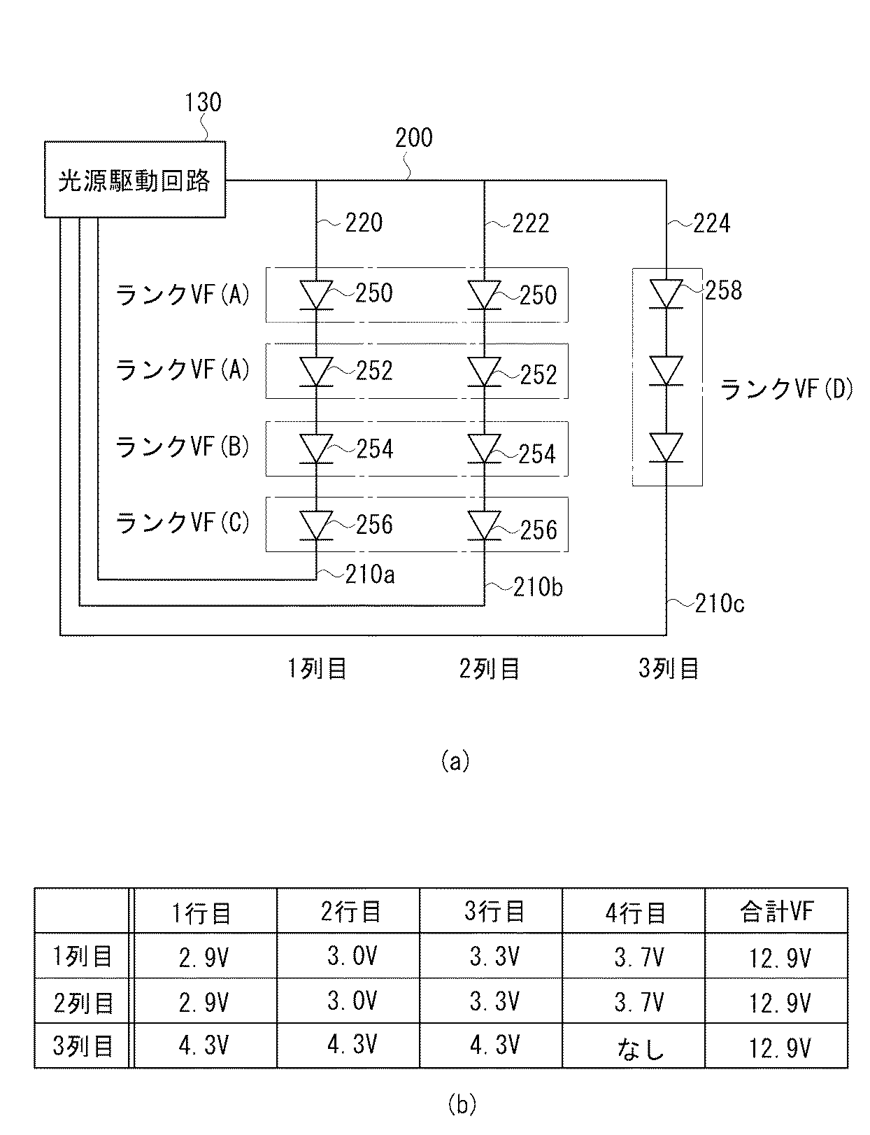
図7は、本実施例に係るバックライト装置において11灯数のLEDを駆動するマトリックス駆動回路の構成を示す。マトリックス駆動回路は、光源駆動回路130に接続されたアノード側の電源ライン200と、カソード側の電源ライン210a、210b、210cと、電源ライン200と210a〜210cの間に並列に接続された電流経路220、222、224とを含む。第1列目の電流経路220は、4つのLEDを直列に接続し、第2列目の電流経路222は、4つのLEDを直列に接続し、第3列目の電流経路224は、3つのLEDを直列に接続する。
FIG. 7 shows a configuration of a matrix drive circuit that drives 11 LEDs in the backlight device according to the present embodiment. The matrix driving circuit includes an anode-
1列目および2列目のLEDの数は等しいが、3列目のLEDの数は、1列目および2列目のLEDの数と異なる。本実施例では、各列のLEDの数が異なるとき、各列のVFの合計値を等しくするか、その差分を限りなく小さくなるようにVFランクの選定を行う。1列目と2列目の電流経路220、222において、1行目のLED250はランクVF(A)であり、VFが2.9Vである。2行目のLED252はランクVF(A)であり、VFが3.0Vである。3行目のLED254はランクVF(B)であり、VFが3.3Vである。4行目のLED256はランクVF(C)であり、VFが3.7Vである。従って、第1列および第2列のLEDのVFの合計値は12.9Vである。他方、3列目の電流経路224において、3つのLED258は、すべてランクVF(D)であり、VFが4.3Vである。従って、VFの合計値は12.9Vである。また、第1ないし第3列の各LED250、252、254、256、258の光度ランクおよび色調ランクは同一であることが望ましい。
The number of LEDs in the first and second rows is equal, but the number of LEDs in the third row is different from the number of LEDs in the first and second rows. In this embodiment, when the number of LEDs in each column is different, the VF rank is selected so that the total value of VFs in each column is equal or the difference is minimized. In the
このようにマトリックス駆動回路を構成することにより、光源駆動回路130から第1および第2の電源ライン200、210a〜c間が定電流制御されることで、各列の順方向電圧の合計が等しくなり、各LEDがバラツキの少ない光度および色調で点灯される。これにより、LEDの総数が割り切れない数または素数であっても、マトリックス駆動回路によりLEDの最適な点灯を行うことができる。
By configuring the matrix driving circuit in this way, the constant current control is performed between the first and second
なお、図7に示すマトリックス駆動回路に示されるランクVFは、一例であって、これに限るものではない。さらに、各列に用いるVFランクの組合せや、各列の合計のVFの値も適宜変更することができる。さらに上記例では、各列の合計のVFを12.9Vとすべて等しくしたが、各列の合計のVFの差分が一定値(例えば、0.1V以内)に抑えるようにしてもよい。 The rank VF shown in the matrix drive circuit shown in FIG. 7 is an example, and the present invention is not limited to this. Furthermore, the combination of VF ranks used for each column and the total VF value of each column can be changed as appropriate. Further, in the above example, the total VF of each column is all equal to 12.9 V, but the difference of the total VF of each column may be suppressed to a constant value (for example, within 0.1 V).
また、11個のLEDを駆動する場合には、図8に示すように、3行×3列とし、4列目の電流経路226に2つのLEDを直列接続する構成であってもよい。各LEDのVFは、図8(b)のテーブルに示すような組合せを用いることができ、4列目のVFの合計は8.7Vであり、その他の各列のVFの合計は8.8Vである。勿論、4列目のVFの合計は8.8Vであることが望ましい。
Further, when eleven LEDs are driven, as shown in FIG. 8, the configuration may be 3 rows × 3 columns and two LEDs connected in series to the
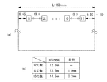
図9(a)は、11個のLEDの配列を説明する図である。液晶表示パネル110を7インチワイドサイズとし、有効表示エリアの長辺の長さLを160mmとする。上記数式1に従うと、各LEDは、約13.3mmの間隔で配置され、左右両端のLEDは、エッジから6.65mmに配置される。図中の四角形の内部の数字は灯数を示す。
FIG. 9A is a diagram illustrating an arrangement of 11 LEDs. The liquid
図9(b)に、LEDを12灯数、11灯数、10灯数としたときのLEDの間隔と、12灯数のときの間隔からの差分を示す。12灯数から10灯数に削減した場合には、LEDの間隔が2.2mmだけ広がるが、11灯数に削減した場合には、間隔が1.0mmとなり、光源にムラができず、表示斑も発生しない。 FIG. 9B shows the difference between the LED interval when the number of LEDs is 12, 11, and 10 and the interval when the number of LEDs is 12. When the number of lamps is reduced from 12 to 10, the distance between the LEDs is increased by 2.2 mm. However, when the number is reduced to 11 lamps, the distance is 1.0 mm, and the light source is not uneven. There are no spots.
図10(a)は、導光板150を使用した液晶表示装置100の模式図である。液晶表示パネル110の背面に導光板150が設置され、導光板150の一側面に沿って光源部140が設置される。光源部140から照射されたライン上の点光源は、導光板150によって直角に反射され面光源として液晶表示パネル110を照射する。図10(b)は、図7に示すマトリックス駆動回路を構成するLEDが直線状に配列されたイメージを示している。また、図10(c)に示すように、図10(b)に示すライン状に配列されたLEDを複数ラインとすることで、LEDの面状光源を得ることも可能である。この場合には、面状光源と液晶表示パネル110の間にLEDの光を拡散する拡散シートなどを介在させるようにしてもよい。
FIG. 10A is a schematic diagram of the liquid crystal display device 100 using the
以上、本発明の好ましい実施の形態について詳述したが、本発明に係る特定の実施形態に限定されるものではなく、特許請求の範囲に記載された本発明の要旨の範囲内において、種々の変形・変更が可能である。 The preferred embodiments of the present invention have been described in detail above. However, the present invention is not limited to the specific embodiments according to the present invention, and various modifications can be made within the scope of the gist of the present invention described in the claims. Deformation / change is possible.
100:液晶表示装置
110:液晶表示パネル
120:バックライト装置
130:光源駆動回路
140:光源部
142:プリント基板
150:導光板
200、210a、210b、210c、210d:電源ライン
220、222、224、226:電流経路
250、252、254、256、258:LED
100: liquid crystal display device 110: liquid crystal display panel 120: backlight device 130: light source driving circuit 140: light source unit 142: printed circuit board 150:
Claims (4)
第1の電源ラインと、
第2の電源ラインと、
第1および第2の電源ライン間に並列に接続された複数の電流経路とを含み、
前記複数の電流経路の各々は、直列に接続された複数の発光素子を含み、前記複数の電流経路に接続された発光素子の総数はn個であり、nは複数の列で割り切れない数または素数であり、
前記複数の電流経路に含まれる第1の電流経路は第1の数の発光素子を含み、前記複数の電流経路に含まれる第2の電流経路は第1の数と異なる第2の数の発光素子を含み、
第1の電流経路に含まれる各発光素子の順方向降下電圧の選定された組合せの配列は、第2の電流経路に含まれる各発光素子の順方向降下電圧の選定された組合せの配列と異なり、
第1の電流経路に含まれる第1の数の発光素子の順方向降下電圧の合計と第2の電流経路に含まれる第2の数の発光素子の順方向降下電圧の合計の差分は等しいかあるいは一定の範囲内である、バックライト装置。 A backlight device in which n light emitting elements that cannot equalize the number of light emitting elements in each column are driven in a matrix, and n light emitting elements are linearly arranged at equal intervals,
A first power line;
A second power line;
A plurality of current paths connected in parallel between the first and second power supply lines,
Number each comprise a plurality of light emitting elements connected in series, the total number of connected light-emitting element to the plurality of current paths is n pieces, n is not divisible by the plurality of rows of the plurality of current paths Or a prime number ,
The first current path included in the plurality of current paths includes a first number of light emitting elements, and the second current path included in the plurality of current paths is a second number of light emission different from the first number. Including elements,
The arrangement of the selected combination of the forward drop voltages of the light emitting elements included in the first current path is different from the arrangement of the selected combination of the forward drop voltages of the light emitting elements included in the second current path. ,
Is the difference between the total forward drop voltage of the first number of light emitting elements included in the first current path equal to the total forward drop voltage of the second number of light emitting elements included in the second current path? Alternatively, a backlight device that is within a certain range.
Priority Applications (1)
| Application Number | Priority Date | Filing Date | Title |
|---|---|---|---|
| JP2007301139A JP5344809B2 (en) | 2007-11-21 | 2007-11-21 | Backlight device |
Applications Claiming Priority (1)
| Application Number | Priority Date | Filing Date | Title |
|---|---|---|---|
| JP2007301139A JP5344809B2 (en) | 2007-11-21 | 2007-11-21 | Backlight device |
Publications (2)
| Publication Number | Publication Date |
|---|---|
| JP2009129591A JP2009129591A (en) | 2009-06-11 |
| JP5344809B2 true JP5344809B2 (en) | 2013-11-20 |
Family
ID=40820337
Family Applications (1)
| Application Number | Title | Priority Date | Filing Date |
|---|---|---|---|
| JP2007301139A Expired - Fee Related JP5344809B2 (en) | 2007-11-21 | 2007-11-21 | Backlight device |
Country Status (1)
| Country | Link |
|---|---|
| JP (1) | JP5344809B2 (en) |
Families Citing this family (6)
| Publication number | Priority date | Publication date | Assignee | Title |
|---|---|---|---|---|
| US8907884B2 (en) * | 2010-01-06 | 2014-12-09 | Apple Inc. | LED backlight system |
| JP2011151268A (en) * | 2010-01-22 | 2011-08-04 | Sharp Corp | Light-emitting device |
| JP6376485B2 (en) * | 2013-03-19 | 2018-08-22 | パナソニックIpマネジメント株式会社 | LED module, lighting apparatus, and method of manufacturing LED module |
| WO2016133008A1 (en) * | 2015-02-19 | 2016-08-25 | シャープ株式会社 | Illuminating device and display device |
| KR20170059541A (en) | 2015-11-20 | 2017-05-31 | 삼성디스플레이 주식회사 | Backlight unit and display apparatus including the same |
| JP7458853B2 (en) | 2020-03-30 | 2024-04-01 | キヤノン株式会社 | Light source device, illumination device, and exposure device. |
Family Cites Families (10)
| Publication number | Priority date | Publication date | Assignee | Title |
|---|---|---|---|---|
| JP2001195904A (en) * | 2000-01-12 | 2001-07-19 | Gc Corp | Roentgen film viewer and display apparatus |
| JP2003068109A (en) * | 2001-08-23 | 2003-03-07 | Sony Corp | Luminaire and projector |
| JP4402336B2 (en) * | 2002-06-26 | 2010-01-20 | 三菱電機株式会社 | Planar light source device and liquid crystal display device using the same |
| JP4670315B2 (en) * | 2004-11-09 | 2011-04-13 | ソニー株式会社 | Backlight device and display device |
| JP4544068B2 (en) * | 2005-07-14 | 2010-09-15 | ソニー株式会社 | Light emitting diode element drive circuit, light source device, display device |
| JP2007065414A (en) * | 2005-08-31 | 2007-03-15 | Sharp Corp | Method for manufacturing backlight |
| JP4575277B2 (en) * | 2005-11-07 | 2010-11-04 | 東芝モバイルディスプレイ株式会社 | Backlight and liquid crystal display device using the same |
| KR101370363B1 (en) * | 2006-10-06 | 2014-03-05 | 코닌클리케 필립스 엔.브이. | A switched light element array and method of operation |
| JP2008293861A (en) * | 2007-05-25 | 2008-12-04 | Sharp Corp | Light-emitting device array and lighting device |
| JP2009059636A (en) * | 2007-09-03 | 2009-03-19 | Imac Co Ltd | Lighting device, and wiring board structure for lighting device |
-
2007
- 2007-11-21 JP JP2007301139A patent/JP5344809B2/en not_active Expired - Fee Related
Also Published As
| Publication number | Publication date |
|---|---|
| JP2009129591A (en) | 2009-06-11 |
Similar Documents
| Publication | Publication Date | Title |
|---|---|---|
| CN102252225B (en) | Surface light source using led and backlight unit having the surface light source | |
| US7597468B2 (en) | Light source of side-edge type LED backlight unit | |
| US8081271B2 (en) | Backlight apparatus and liquid crystal display apparatus | |
| EP1640792B1 (en) | Backlight assembly and display apparatus having the backlight assembly | |
| CN101482629B (en) | Backlight, back-light drive device, and display device | |
| US7641352B2 (en) | LED backlight device with deviated LED pitch | |
| RU2451237C2 (en) | Lighting fixture and display device, in which it is used | |
| US20070236447A1 (en) | Backlight unit using light emitting diode | |
| US20100059767A1 (en) | Surface Light-Emitting Device and Display Device Using the Same | |
| US20060087866A1 (en) | LED backlight | |
| US20060279671A1 (en) | Backlight assembly for liquid crystal display device and liquid crystal display device using the same | |
| JP5344809B2 (en) | Backlight device | |
| KR101881065B1 (en) | Light source module and backlight unit | |
| JP2006040764A (en) | Surface light source and liquid crystal display | |
| US20090091947A1 (en) | Surface light source structure of backlight module in a flat panel display | |
| US20090168456A1 (en) | Light source module for a display device and a display device having the same | |
| US7588363B2 (en) | Illuminat system | |
| JP2008117595A (en) | Led light source unit and backlight device | |
| KR101259064B1 (en) | Backlight unit, Liquid crystal display module including the same | |
| US20070064443A1 (en) | Led backlight for flat panel display | |
| TWI757935B (en) | A backlight module and a layout method of light-emitting diodes | |
| US20120307482A1 (en) | Planar light source and backlight unit having the same | |
| JP2011040664A (en) | Surface light source and liquid crystal display device | |
| US10962829B1 (en) | Light bar, backlight module and display device | |
| US20050281026A1 (en) | Multicolor light source and backlight module using the same |
Legal Events
| Date | Code | Title | Description |
|---|---|---|---|
| A621 | Written request for application examination |
Free format text: JAPANESE INTERMEDIATE CODE: A621 Effective date: 20101022 |
|
| A521 | Request for written amendment filed |
Free format text: JAPANESE INTERMEDIATE CODE: A523 Effective date: 20111216 |
|
| A977 | Report on retrieval |
Free format text: JAPANESE INTERMEDIATE CODE: A971007 Effective date: 20120426 |
|
| A131 | Notification of reasons for refusal |
Free format text: JAPANESE INTERMEDIATE CODE: A131 Effective date: 20120508 |
|
| A521 | Request for written amendment filed |
Free format text: JAPANESE INTERMEDIATE CODE: A523 Effective date: 20120622 |
|
| A131 | Notification of reasons for refusal |
Free format text: JAPANESE INTERMEDIATE CODE: A131 Effective date: 20120807 |
|
| A521 | Request for written amendment filed |
Free format text: JAPANESE INTERMEDIATE CODE: A523 Effective date: 20121004 |
|
| A02 | Decision of refusal |
Free format text: JAPANESE INTERMEDIATE CODE: A02 Effective date: 20130305 |
|
| A521 | Request for written amendment filed |
Free format text: JAPANESE INTERMEDIATE CODE: A523 Effective date: 20130528 |
|
| A911 | Transfer to examiner for re-examination before appeal (zenchi) |
Free format text: JAPANESE INTERMEDIATE CODE: A911 Effective date: 20130604 |
|
| TRDD | Decision of grant or rejection written | ||
| A01 | Written decision to grant a patent or to grant a registration (utility model) |
Free format text: JAPANESE INTERMEDIATE CODE: A01 Effective date: 20130813 |
|
| A61 | First payment of annual fees (during grant procedure) |
Free format text: JAPANESE INTERMEDIATE CODE: A61 Effective date: 20130813 |
|
| R150 | Certificate of patent or registration of utility model |
Ref document number: 5344809 Country of ref document: JP Free format text: JAPANESE INTERMEDIATE CODE: R150 Free format text: JAPANESE INTERMEDIATE CODE: R150 |
|
| LAPS | Cancellation because of no payment of annual fees |