JP4532637B2 - Data reordering device - Google Patents
Data reordering device Download PDFInfo
- Publication number
- JP4532637B2 JP4532637B2 JP2000002468A JP2000002468A JP4532637B2 JP 4532637 B2 JP4532637 B2 JP 4532637B2 JP 2000002468 A JP2000002468 A JP 2000002468A JP 2000002468 A JP2000002468 A JP 2000002468A JP 4532637 B2 JP4532637 B2 JP 4532637B2
- Authority
- JP
- Japan
- Prior art keywords
- stage
- shift register
- code
- bit
- pseudo
- Prior art date
- Legal status (The legal status is an assumption and is not a legal conclusion. Google has not performed a legal analysis and makes no representation as to the accuracy of the status listed.)
- Expired - Fee Related
Links
Images


Description
【0001】
【発明の属する技術分野】
本発明はデータ順序変更装置に関し、例えば、CDMA(符号分割多元接続)方式などのディジタル通信方式において、符号化や復号化処理の過程でブロックインタリーブなどを行う場合に適用し得るものである。
【0002】
【従来の技術】
従来のブロックインタリーブ方式としては、次の参考文献1、参考文献2に示されるようなものがある。
【0003】
参考文献1:ANSI/TIA/EIA−95−B,page7−3
参考文献2:ANSI/TIA/EIA−95−B,page7−12
参考文献1は、図3に示すように、符号化の処理手順を示している。
【0004】
図3において、ブロックインタリーブ(Block Interleaver)23,27,36は、畳込み符号化(Convolutional Encoder)21,25,34が行われ、さらにシンボルリピティション(Symbol Repetition)22,26,35が行われた後に実行される。
【0005】
したがってこれに対応して受信側で行われる復号化の過程においては、これら3者のうちでは、まず最初に、インタリーバ処理23,27,28の結果を各インタリーバ処理前の状態に戻すデインタリーバ処理が行われ、次に、リピテション処理22,26,35の結果を各リピテション処理前の状態に戻すデリピテション処理が行われ、最後に、畳込み符号化21,25,34の結果を各畳み込み符号化処理前の状態に戻すために、例えばビタビ復号処理が行われる。
【0006】
一方、前記参考文献2はブロックインタリーブの処理手順を示している。
【0007】
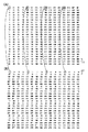
参考文献2には、図2(A)および(B)に示すように、横方向に16個、縦方向に24個の成分を持つマトリクスから構成された2つのテーブル1T、2Tが記載されている。
【0008】
このうちテーブル1Tの方は、インタリーバ処理の入力、すなわちバッファメモリへの書き込み操作を記述したもので、384シンボルの入力データ系列は、1シンボルずつ順番に、1行1列(アドレス番号1)、2行1列(アドレス番号2)、3行1列(アドレス番号3)、…24行1列(アドレス番号24)、1行2列(アドレス番号25)、2行2列(アドレス番号26)、…、24行16列(アドレス番号384)に書き込まれる。
【0009】
したがってこのテーブル1Tはそのまま、当該バッファメモリを示しているととらえることができる。そしてテーブル1Tの各アドレスのアドレス番号は、384シンボルの入力データ系列の本来の順番をも示している。
【0010】
すなわち、アドレス番号1に書き込まれたデータは、384シンボルのデータ系列中で順番が1番目のデータであり、アドレス番号2に書き込まれたデータは、当該384シンボル中の順番が2番目のデータであり、…、アドレス番号384に書き込まれたデータは、当該384シンボル中で順番が384番目のデータである。
【0011】
このとき当該バッファメモリ(すなわちテーブル1T)のアドレス番号1(1行1列)に書き込まれたデータをx(1)とし、アドレス番号2に書き込まれたデータをx(2)とし、アドレス番号3に書き込まれたデータをx(3)とし、…、アドレス番号384に書き込まれたデータをx(384)とする。
【0012】
一方、テーブル(読み出し順位テーブル)2Tの方は、インタリーバ処理の出力、すなわち当該バッファメモリからの当該入力データ系列の読み出し操作を記述したものである。16行24列のマトリクス上で対応する位置にある前記バッファメモリ1Tの(アドレス番号によって一義的に指定される)メモリセルからの読み出しが行われる順位が、当該テーブル2Tの各アドレスに格納されている。
【0013】
すなわち、テーブル2Tの1行1列には前記バッファメモリ1T上で1行1列であるアドレス番号1のセルの読み出し順位を示す「1」が格納されており、以降も同様に、2行1列には前記バッファメモリの2行1列であるアドレス番号2セルの読み出し順位を示す「65」が、3行1列には前記バッファメモリの3行1列であるアドレス番号3のセルの読み出し順位を示す「129」が、…、24行16列には前記バッファメモリの24行16列であるアドレス番号384のセルの読み出し順位を示す「384」が格納されている。
【0014】
したがって、図2(A)のテーブル1Tを用いてインタリーバ処理の入力(バッファメモリ1Tへの書き込み)を行い、図2(B)のテーブル2Tを用いてインタリーバ処理の出力(バッファメモリ1Tからの読み出し)を行う場合、バッファメモリ1Tの各アドレスに書き込まれている384シンボルのデータx(1)〜x(384)のうち、バッファメモリ1Tの1行1列のx(1)がテーブル2Tの1行1列の読み出し順位1に応じて最初に読み出され、続いてバッファメモリ1Tの1行9列のx(193)がテーブル2Tの1行9列の読み出し順位2に応じて2番目に読み出され、続いてバッファメモリ1Tの1行5列のx(97)がテーブル2Tの1行5列の読み出し順位3に応じて3番目に読み出され、…、最後に、バッファメモリ1Tの24行16列のx(384)がテーブル2Tの24行16列の読み出し順位384に応じて384番目に読み出される。
【0015】
この操作により、バッファメモリ1Tへの書き込み前(および書き込み時点)では、
x(1)、x(2)、x(3)、x(4)、x(5)、…、x(382)、x(383)、x(384)の順番であったデータ系列DS1が、読み出し後には、
x(1)、x(193)、x(97)、x(289)、x(49)、…、x(288)、x(192)、x(384)の順番のデータ系列DS2に変換される。
【0016】
これは、バッファメモリ1Tに対して画一的に縦方向に書き込んだデータ系列DS1を、(任意の1つの行の内部では順番を変化させながらも)横方向に読み出すことで、データ系列DS2を得ている。
【0017】
このデータ系列DS2を受け取った受信側で行われるデインタリーバ処理では、これと逆の操作を行う(横方向に書込み、縦方向に読出す)ことにより、元の順序のデータ系列DS1を復元することができる。
【0018】
このようなインタリーブ処理およびデインタリーブ処理(インタリーバ処理およびデインタリーバ処理)を行うことにより、伝搬路でバースト誤り(集中的な誤り)が発生しても、復号過程において、受信したデータ系列DS2がDS1に変換される時に、当該誤りを元のデータ系列DS1上に分散させて誤りのバースト性を解消することができるので、ビタビ復号などのバースト誤りに弱い復号を行う場合、復号特性を改善することが可能である。
【0019】
【発明が解決しようとする課題】
ところで、前記バースト誤りのバースト性をできるだけ完全に解消し、当該誤りを、前記デインタリーバ処理によって復元されたデータ系列DS1上で真に偏りなく分散させるためには、インタリーバ処理の規則性に偏りがなく、白色雑音的なランダム(無相関)性があることが求められる。
【0020】
特に、畳み込み符号化を行った後にランダムインタリーバ処理を施してつくられるターボ符号の場合、当該ランダムインタリーバ処理では、高い白色雑音性が求められる。
【0021】
ターボ符号の場合もその他の符号の場合も、インタリーバ処理(ランダムインタリーバ処理)の配列操作に少しでも白色雑音的でなく偏った部分があると、その偏りの部分につき、デインタリーバ処理の後でも、バースト誤りのバースト性が残留する可能性があり、その残留バースト部分のために復号特性が劣化し得る。
【0022】
例えば、図2(B)のテーブル2Tの各列を縦方向にみると明らかなように、各列の1行目には1〜16までの数字が並び、各列の2行目には65〜80の数字が並び、各列の3行目には129〜144の数字が並び、…、各列の7行目には33〜48の数字が並び、…、各列の24行目には369〜384の数字が並んでおり、この配列にはある種の周期性と偏りが内在している。
【0023】
また、図2(B)のテーブル2Tでは、任意の1行の内部では読み出し順位を示す数字はランダムに配置されているように見えるが、例えば1〜16の数字を配列した1行目では、左端の1列目に「1」、9列目に「2」、5列目に「3」、…、16列目に「16」が配置されているが、この1行目と比較しながら、65〜80の数字を配列した2行目を見ると、2行目の左端の1列目には、当該65〜80の範囲で最も小さな「65」が配置され、9列目には当該65〜80の範囲で2番目に小さな「66」が配置され、5列目には当該65〜80の範囲で3番目に小さな「67」が配置され、…、16列目には当該65〜80の範囲で最も大きな「80」が配置されている。この関係は、3行〜24行にも当てはまる。
【0024】
すなわち、一見すると規則性がないように見えるテーブル2Tは、各行内での配列規則はまったく同じで画一的であり、明確な周期性と偏りを内包している。
【0025】
このような周期性や偏りを利用すれば、前記バッファメモリに対する書き込みアドレスや読み出しアドレスを生成するための書込み/読出しアドレス生成回路を実現することは比較的容易であると考えられるが、上述した白色雑音的なランダム性を保証することは難しい。
【0026】
白色雑音的な配列パターンをテーブル2Tのなかに再現することができたとしても、送信側、受信側でテーブル2Tと同様な内容を持ったROM(リードオンリーメモリ)テーブルなどを装備し、当該ROMテーブルを参照することで読み出し順位を決定するルックアップ方式によってインタリーバ処理やデインタリーバ処理を実行することが必要となって、ハードウエア規模が増大するという問題がある。
【0027】
また、いっそう長い周期のインタリーバ処理を行う必要が生じた場合、行列(マトリクス)の大きさ(縦×横)が大きくなるほどテーブル2Tの規模は拡大し、ROMテーブルの規模も拡大することとなって、さらにハードウエア規模が増大する。
【0028】
また、データレートの種類が多くなればその種類分のROMテーブルが必要となり、これによってもハードウエア規模が増大してしまう。
【0029】
【課題を解決するための手段】
かかる課題を解決するために、本発明では、縦方向にM、横方向にNのM×Nの成分を有するマトリクス状に情報系列を一時的に記憶するための複数のセルを有する一時記憶手段を備え、当該一時記憶手段に対する情報の書き込み順序又は読み出し順序を制御することで、データ順序変更処理を行うデータ順序変更装置において、0以外の初期値が設定されたm段のシフトレジスタと、前記m段のシフトレジスタの最終段のビット値と1段目のビット値とを加算して前記m段のシフトレジスタの1段目に入力する加算器とを有し、クロックに同期して前記m段のシフトレジスタにおけるビットシフトを実行することにより、前記マトリクスの縦方向成分を指定する第1の擬似雑音符号を発生する第1の符号発生手段と、0以外の初期値が設定されたn段のシフトレジスタと、前記n段のシフトレジスタの最終段のビット値と1段目のビット値とを加算して前記n段のシフトレジスタの1段目に入力する加算器とを有し、前記クロックに同期して前記n段のシフトレジスタにおけるビットシフトを実行することにより、前記マトリクスの横方向成分を指定する第2の擬似雑音符号を発生する第2の符号発生手段とを備え、前記マトリックスは、前記Mが2 m −1であり、前記Nが2 n −1であり、前記データ順序変更装置は、前記第1の符号発生手段により指定される前記マトリクスの縦方向成分と、前記第2の符号発生手段により指定される前記マトリクスの横方向成分とにより特定される前記一時記憶手段内のセルに対して情報の書き込み又は読み出しを行うことを特徴とする。
【0030】
【発明の実施形態】
(A)実施形態
以下、本発明のデータ順序変更装置を、シフトレジスタ型のPN(擬似雑音)符号発生器を用いたCDMAの符号化装置におけるインタリーバ処理部に適用した場合を例に、第1〜第3の実施形態について説明する。
【0031】
(A−1)第1の実施形態の構成および動作
本実施形態の符号化装置50の主要部の構成を図4に示す。図4は、図3に示した一連の符号化処理手順のうち、インタリーバ処理(例えばBlock Interleaver23)に対応する部分を中心に一部だけを図示している。
【0032】
図4において、当該符号化装置50は、リピテション処理部51と、インタリーバ処理部(ランダムインタリーバ)52と、加算器53とを備えている。
【0033】
このうちリピテション処理部51は、上述したシンボルリピテション(Symbol Repetition)処理部(例えばSymbol Repetition22)に対応するリピテション処理を行い、リピテション処理の結果として得られるデータ系列DS3を出力する部分である。
【0034】
必要に応じて当該シンボルリピテション処理部51は省略してもよく、その他の処理部(例えばパンクチャ処理部など)と置換してもよい。省略した場合にはインタリーバ処理部52の前段に、畳み込み符号化処理部(例えば前記Convolutional Encoder21)が配置されることになる。
【0035】
リピテション処理部51からデータ系列DS3を受け取るインタリーバ処理部52は、バッファメモリ(RAM(ランダムアクセスメモリ))54と、書き込みアドレス指定回路55と、読み出しアドレス指定回路56とを備えている。
【0036】
バッファメモリ54は、上述したバッファメモリ1Tに対応する構成部分であり、図5(A)に示すようなマトリクス状の構造を持っているものとする。図5(A)に示したマトリクス上の各セルのアドレスは、左の列ほど下位で、同一列内では上の行ほど下位であるものとする。
【0037】
すなわち、1行1列目のセルが最下位のアドレス番号1に対応し、2行1列目のセルが最下位から2番目のアドレス番号2に対応し、3行1列のセルが最下位から3番目のアドレス番号3に対応し、…、7行15列目が最下位から105番目(すなわち最上位)に対応するものとする。
【0038】
したがって、図5(A)に7行15列のマトリクスに示した各数字は、当該マトリクス上で各数字が存在する位置のメモリセルのアドレス番号を示しているとみることもできる。
【0039】
書き込みアドレス指定回路55は、データ系列DS3の各シンボルをバッファメモリ54に書き込むにあたって、アドレス指定を行う回路である。本実施形態における書き込みアドレス指定回路55によるアドレス指定は、バッファメモリ54上では、メモリアドレスの最下位から上位へ向けて逐次、書き込みアドレス指定回路55が持っているアドレスポインタ値を、画一的にインクリメントするものとする。
【0040】
もちろん、最上位から下位へデクリメントするような構成も可能である。
【0041】
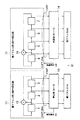
一方、読み出しアドレス指定回路56は、バッファメモリ54に書き込まれたデータ系列DS3を読み出すにあたってアドレス指定する回路で、PN符号を用いて読み出しアドレスを指定するために、図1に示すような内部構成を備えている。
【0042】
(A−1−1)読み出しアドレス指定回路の内部構成および動作
図1において、読み出しアドレス指定回路56は、シフトレジスタ型の2つのPN(符号)発生器11および12を備えている。
【0043】
このうちPN符号発生器11は、バッファメモリ54のマトリクスにつき、縦アドレス(縦方向成分)PAを指定するための回路で、PN符号発生器12は、バッファメモリ54の当該マトリクスにつき、横アドレス(横方向成分)HAを指定するための回路である。
【0044】
PN符号発生器11は、3ビットのシフトレジスタ1〜3と、1つの加算器15を備えており、レジスタ1,2,3はこの順番でシリアルに接続され、加算器15の2つの入力端子にはレジスタ1の出力端子とレジスタ3の出力端子が接続されており、加算器15の出力端子はレジスタ1の入力端子に接続されており、レジスタ1〜3の出力端子からパラレル出力される3ビットによって、前記縦アドレスPAが指定される。
【0045】
例えば、レジスタ1と2の出力がともに“0”で、レジスタ3の出力が“1”である001Bの場合には、縦アドレスPAの値は1Dとなり、レジスタ1の出力が“1”で、レジスタ2と3の出力がともに“0”である100Bの場合には、縦アドレスPAの値は4Dとなる。
【0046】
なお、ここで「D」はその前の数字が10進数表示であることを示し、「B」はその前の数字が2進数表示であることを示す。以下においても同じである。
【0047】
これに対しPN符号発生器12は、4ビットのシフトレジスタ4〜5と、1つの加算器16を備えており、レジスタ4,5,6,7はこの順番でシリアルに接続され、加算器16の2つの入力端子にはレジスタ4の出力端子とレジスタ7の出力端子が接続され、加算器16の出力端子にはレジスタ4の入力端子が接続され、レジスタ4〜7の出力端子からパラレルに取り出される4ビットによって、前記横アドレスHAが指定される。
【0048】
例えば、レジスタ4〜6の出力がすべて“0”で、レジスタ7の出力が“1”である0001Bの場合には横アドレスPAの値は1Dとなり、レジスタ4の出力が“1”で、レジスタ5〜7の出力がすべて“0”である1000Bの場合には縦アドレスPAの値は8Dとなる。
【0049】
そして、例えば、レジスタ1〜3の出力が001Bで、レジスタ4〜7の出力が0001Bであるとき、当該読み出しアドレス指定回路56の指定するバッファメモリ54のメモリセルは1行1列のアドレス番号1のセルである。同様に、レジスタ1〜3の出力が001Bで、レジスタ4〜7の出力が1000Bであるとき、当該読み出しアドレス指定回路56の指定するバッファメモリ54のメモリセルは1行8列のアドレス番号50のセルとなる。
【0050】
このようなPN符号発生器11と12の構成を一般化すると、バッファメモリ54のマトリクスが縦方向にM、横方向にNのM×N(M=2m−1,N=2n−1、ここでm,nは自然数)構造を持つ場合、PN符号発生器11のシフトレジスタはm段(mビット)になるとともにPN符号発生器12のシフトレジスタはn段(nビット)になる。
【0051】
本実施形態は、このような一般形に関し、m=3,n=4と置いた例である。
【0052】
本実施形態においては、縦アドレス用PN発生器11は3段PN発生器であり、横アドレス用PN発生器12は4段PN発生器であるため、それぞれ周期7(23−1)シフト、周期15(24−1)シフトでレジスタの内部状態の変化がちょうど1巡する。
【0053】
レジスタの初期値については全て0でなければどのような値でも構わないが、ここではそれぞれ(レジスタ1,レジスタ2,レジスタ3)=(0,0,1)、(レジスタ4、レジスタ5、レジスタ7)=(0,0,0,1)とする。この初期状態001B、0001Bは10進数表現ではいずれも1Dを指定しており、縦3段、横4段を合わせると、上述したバッファメモリ54の1行1列目に位置する最下位アドレスのセルを指定している。
【0054】
縦アドレス用PN発生器11のレジスタの内部状態の変化は、001,100,110,111,011,101,010までで1周期であり、以降はまた001、…と変化するので、縦アドレスの10進数表示は1,4,6,7,3,5,2(ここまでで縦アドレスの1周期(縦アドレス周期)),1、…と変化する。
【0055】
同様に、横アドレス用PN発生器12のレジスタの内部状態の変化は、0001、1000、1100、1110、1111、0111、1101、0101、1010、1101、0110、0011、1001、0100、0010までで1周期であり、以降はまた0001、…と変化するので、横アドレスの10進数表示は1,8,12,14,15,7,11,5,10,13,6,3,9,4,2(ここまでで横アドレスの1周期(横アドレス周期)),1、…と変化する。
【0056】
ここで、レジスタ1〜3のシフト動作と、レジスタ4〜7のシフト動作がともに初期状態001B、0001Bから始まり、同じクロックを基に1クロックにつき1回(1ビット)シフトすることで進行するものとすると、前記縦アドレス周期は7クロック(7シフト)に相当し、前記横アドレスの1周期は15クロック(15シフト)に相当する。
【0057】
したがって、縦アドレスと横アドレスを組み合わせた合成アドレスの1周期(合成アドレス周期)は、105クロックに相当するものとなり、ちょうど105クロックで、図5(B)の読み出し順位マトリクス(インタリーブマトリクス、すなわち読み出し順位テーブル)57に示す1〜105番の読み出しを、漏れなく、なおかつ重複なく行うことができる。
【0058】
図5(B)と図5(A)の関係は、上述した図2(B)と図2(A)の関係と同じである。
【0059】
すなわち、7行16列のマトリクス上で対応する位置にある前記バッファメモリ54のアドレス番号(メモリセル)からの読み出しが行われる順位が、当該読み出し順位テーブル57の各位置に配置されている。
【0060】
ただし本実施形態の場合、読み出し順位テーブル57は従来のテーブル2Tと異なり、ROMなどのハードウエア的な大規模記憶手段の実体を伴わない概念的なテーブルであり、読み出し順位テーブル57中の各数字は、いずれかの記憶手段に格納された論理的なデータではなく、初期時点(縦アドレスPAおよび横アドレスHAがともに1Dとなるテーブル57の1行1列の「1」に対応する時点)から該当する時点までの、シフトレジスタの総シフト数(あるいは当該シフトのために供給された総クロック数)に対応した物理的、時間的な概念である。
【0061】
換言するなら読み出し順位テーブル57は、読み出しアドレス指定回路56の指定する読み出しアドレスHA+PAの変化をまとめると、図5(B)のように図示することができることを示しているにすぎない。PN符号発生器11,12を構成するシフトレジスタも広い意味でとらえると記憶手段の一種ではあるが、同等な機能をサポートできるROMなどに比較すると、はるかに小規模である。
【0062】
上述した書き込みアドレス指定回路55の指定する書き込みアドレスにしたがってバッファメモリ54のアドレス番号1のセルに書き込まれたデータ系列DS3中のデータをx(1)とし、同様に、バッファメモリ54のアドレス番号2のセルに書き込まれたデータ系列DS3中のデータをx(2)、バッファメモリ54のアドレス番号3のセルに書き込まれたデータ系列DS3中のデータをx(3)、…、バッファメモリ54のアドレス番号105のセルに書き込まれたデータ系列DS3中のデータをx(105)とする。
【0063】
すなわち、データ系列DS3中の各データは、x(1)、x(2)、x(3)、x(4)、x(5)、x(6)、x(7)、…、x(103)、x(104)、x(105)の順番である。
【0064】
これに対し、読み出しアドレス指定回路56が指定する読み出しアドレスHA+HPにしたがったバッファメモリ54からの読み出しは、x(1)、x(53)、x(83)、x(98)、x(101)、x(47)、x(72)、…、x(59)、x(26)、x(9)の順番で行われ、これらがインタリーバ処理を受けたデータ系列DS4としてインタリーバ処理部52から加算器53に供給される。
【0065】
加算器53では、このインタリーバ処理済みのデータ系列DS4にWalsh関数(例えば図3中のWalsh Function32に相当する)が加算されて出力される。
【0066】
(A−2)第1の実施形態の効果
本実施形態によれば、偏りがなく、白色雑音的にランダム(無相関)な規則性でインタリーバ処理を行うことができるので、インタリーブ後の平均的なデータ聞距離を確保することが可能であり、誤りのバースト性の除去性能に優れたインタリーバ処理を提供することができる。
【0067】
これにより、ビタビ復号やターボ復号の特性を改善することが可能である。
【0068】
また、本実施形態では、従来のようにROMテーブルを用いる場合と比較して、ハードウエア規模が極めて小さい。
【0069】
(B)第2の実施形態
本実施形態は、第1の実施形態と機能面で共通する点が多いので、以下では、本実施形態が第1の実施形態と相違する点についてのみ説明する。
【0070】
実質的にこの相違点は、主として読み出しアドレス指定回路(56)に関連する部分に限られる。
【0071】
(B−1)第2の実施形態の構成および動作
本実施形態の符号化装置60の主要部の構成を図4に示す。本実施形態の符号化装置60は、第1の実施形態の符号化装置50中の読み出しアドレス指定回路56に置換して、読み出しアドレス指定回路61を備え、バッファメモリ54に置換してバッファメモリ62を備えた構成を有している。
【0072】
本実施形態のバッファメモリ62は、図8(A)に示すように、5行12列のマトリクス構造を有している点を除けば、第1の実施形態のバッファメモリ54と同じである。
【0073】
第1の実施形態では、バッファメモリ54のマトリクス構造が7行15列で、縦方向セル数Mも横方向セル数Nも、m、nを自然数として、M=2m−1、N=2n−1の形で記述することができるという意味で、マトリクス構造がPN発生器11,12の各シフトレジスタの1周期と過不足なく一致したが、本実施形態の5行12列のマトリクス構造では、このような一致を得ることはできない。
【0074】
また、本実施形態のバッファメモリ62のマトリクス構造の縦方向Mの5(セル)と横方向Nの12(セル)は、互いに素な関係にある。
【0075】
本実施形態でも、縦アドレス用のPN発生器11は3段シフトレジスタなので、当該PN発生器11の1周期は7クロック分で、縦方向に5セル(通常は5クロック分に相当)しか持たないバッファメモリ62に対しては2クロック分過剰である。
【0076】
同様に、本実施形態の横アドレス用のPN発生器12は4段シフトレジスタなので、当該PN発生器12の1周期は15クロック分で、横方向に12セル(通常は12クロック分に相当)しか持たないバッファメモリ62に対しては、3クロック分過剰である。
【0077】
このようなバッファメモリの構造とシフトレジスタの段数との不一致は、その取り扱いによっては、バッファメモリのすべてのセルを活用できないことで利用効率を低下させたり、インタリーバ処理とそれに対応して受信側で行われるデインタリーバ処理の正常な対応関係を確保することが困難になることも考えられる。
【0078】
本実施形態において、この問題に関する対応策を提供するのが、読み出しアドレス指定回路61である。
【0079】
この読み出しアドレス指定回路61の内部構成を図6に示す。
【0080】
(B−1−1)読み出しアドレス指定回路の構成および動作
図6において、読み出しアドレス指定回路61は、シフトレジスタ型の2つのPN符号発生器11および12と、縦アドレス用の判定器13と、横アドレス用の判定器14とを備えている。
【0081】
このうち判定器13、14以外の第1の実施形態と同一の符号を付した構成要素1〜7,11,12、15,16の構成および動作は、第1の実施形態と実質的に同じである。
【0082】
ただしPN発生器11、12は、第1の実施形態で述べたすべての動作を行う機能に加えて、判定器13,14から更新信号PR、HRの供給を受けるたびに、通常のシフトを行う次のクロックの供給前であっても、1クロック分シフトする機能を装備している。
【0083】
判定器13は、上記縦アドレス用PN発生器11が出力する縦アドレス候補PAPが、前記M(=5D)よリ大きいかどうか判定を行い、もし、M以下の値であれば当該縦アドレス候補PAPを縦アドレスPAとしてそのまま出力するが、Mより大きい値であれば縦アドレス用PN発生器11のSHIFT_ENA端子に更新信号PRを供給してシフトレジスタ1〜3の値を1ビット分シフトさせて更新し、次の縦アドレス候補PAPの出力を要求する。
【0084】
このような操作は、縦アドレス候補PAPとして、前記M以下の値が得られるまで繰り返される。
【0085】
判定器14も同様に、横アドレス用PN発生器12が出力する横アドレス候補HAPについてN(=12D)よりも大きいかどうか判定を行い、もし、N以下の値であれば横アドレスHAとしてそのまま出力するが、Nより大きい値であれば横アドレス用PN発生器12のSHIFT_ENA端子へ更新信号HRを供給してシフトレジスタ4〜7の値を1ビット分シフトさせて更新し、次の横アドレス候補HAPの出力を要求する。
【0086】
このような操作は、横アドレス候補HAPとして、前記N以下の値が得られるまで繰り返される。
【0087】
なお、本実施形態の図8(B)は、第1の実施形態における図5(B)に相当する読み出し順位マトリクス(読み出し順位テーブル)63を示している。
【0088】
本実施形態では、縦アドレスPAと横アドレスHAを組み合わせた合成アドレスの1周期は、60クロックに相当するものとなり、ちょうど60クロックで、図8(B)の読み出し順位マトリクス(読み出し順位テーブル)62に示す1〜60番の読み出しを、漏れなく、なおかつ重複なく行うことができる。
【0089】
第1の実施形態と同様の操作により、縦アドレス用PN発生器11が出力する縦アドレス候補PAPの値は10進数表示で1,4,6,7,3,5,2,1、…の順序で変化し、横アドレス用PN発生器12が出力する横アドレス候補HAPの値は10進数表示で1,8,12,14,15,7,11,5,10,13,6,3,9,4,2,1、…の順序で変化する。
【0090】
このとき判定器13は、上記縦アドレス候補PAPが6Dのときと7Dのときに更新信号PRを出力して、通常1回のシフトを行う1クロック期間に3回シフトを行い7Dの次の3Dを縦アドレスPAとして出力することになる。
【0091】
判定器13のこの動作は周期的なので、判定器13から出力される縦アドレスPAは10進数表示で、1,4,3,5,2,1、…の順序で変化する。
【0092】
同様に、判定器14は、上記横アドレス候補HAPが13D、14D、15Dのときに更新信号HRを出力するので、横アドレス7Dを出力するためには、通常1回のシフトを行う1クロック期間に3回シフトを行い15Dの次の7Dを横アドレスHAとして出力することになり、横アドレス6Dを出力するためには、通常1回のシフトを行う1クロック期間に2回シフトを行い13Dの次の6Dを横アドレスHAとして出力することになる。
【0093】
判定器14のこの動作は周期的なので、判定器14から出力される横アドレスHAは、10進数表示で1,8,12,7,11,5,10,6,3,9,4,2,1、…の順序で変化する。
【0094】
したがって、判定器13から出力される縦アドレスPAと、判定器14から出力される横アドレスHAとを組み合わせた合成アドレスの周期は、上述した60(=5×12)クロックになる。
【0095】
本実施形態により、x(1)、x(2)、x(3)、x(4)、x(5)、x(6)、x(7)、…、x(58)、x(59)、x(60)の順番を持つデータ系列DS3中の各データの順番は、x(1)、x(39)、x(60)、x(33)、x(52)、x(21)、x(49)、…、x(45)、x(18)、x(7)に変換される。
【0096】
(B−2)第2の実施形態の効果
本実施形態によれば、第1の実施形態で得られる効果と同等な効果を得ることができる。
【0097】
加えて、本実施形態によれば、バッファメモリ(62)のマトリクス構造M×Nが、M=2m−1、N=2n−1の形で記述することができる場合はもちろん、できない場合でも、当該MとNが互いに素であることを条件として、バッファメモリのすべてのセルを活用することで利用効率を高く維持し、インタリーバ処理とそれに対応して受信側で行われるデインタリーバ処理の正常な対応関係を確保することが容易であるため、第1の実施形態よりも実装上、設計上の自由度が高く、信頼性も向上する。
【0098】
(C)第3の実施形態
本実施形態は、第1の実施形態と機能面で共通する点が多いので、以下では、本実施形態が第1の実施形態と相違する点についてのみ説明する。
【0099】
実質的にこの相違点は、主として読み出しアドレス指定回路(56)に関連する部分に限られる。
【0100】
一方、第2の実施形態と本実施形態の関係については、第2の実施形態がバッファメモリ(62)のマトリクス構造の縦方向のセル数Mと横方向のセル数Nとは、互いに素であることが必要であったが、本実施形態は、MとNが任意の自然数である場合(M、Nが互いに素である場合も含む)に適用することができる点が相違する。
【0101】
MとNが互いに素でない場合には、前記合成アドレス周期がM×Nよりも小さくなってしまう問題がある。合成アドレス周期がM×Nよりも小さくなるということは、バッファメモリ(62)中のM×N個のすべてのセルからデータを読み出すことができず、正常にインタリーバ処理を行うことができない可能性があることを意味する。
【0102】
(C−1)第3の実施形態の構成および動作
本実施形態の符号化装置70の主要部の構成を図4に示す。本実施形態の符号化装置70は、第1の実施形態の符号化装置50中の読み出しアドレス指定回路56に置換して、読み出しアドレス指定回路71を備え、バッファメモリ54に置換してバッファメモリ72を備えた構成を有している。
【0103】
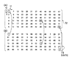
本実施形態のバッファメモリ72は、図9(A)に示すように、6行12列のマトリクス構造を有している点を除けば、第1の実施形態のバッファメモリ54と同じである。
【0104】
第1の実施形態では、バッファメモリ54のマトリクス構造が7行15列で、縦方向セル数Mも横方向セル数Nも、m、nを自然数として、M=2m−1、N=2n−1の形で記述することができるという意味で、マトリクス構造がPN発生器11,12の各シフトレジスタの1周期と過不足なく一致したが、本実施形態の6行12列のマトリクス構造では、このような一致を得ることはできない。
【0105】
また、本実施形態のバッファメモリ72のマトリクス構造の縦方向Mの6(セル)と横方向Nの12(セル)は、互いに素な関係にない点で、第2の実施形態のバッファメモリ62とも相違する。
【0106】
本実施形態でも、縦アドレス用のPN発生器11は3段シフトレジスタなので、当該PN発生器11の1周期は7クロック分で、縦方向に6セル(通常は6クロック分に相当)しか持たないバッファメモリ72に対しては1クロック分過剰である。
【0107】
同様に、本実施形態の横アドレス用のPN発生器12は4段シフトレジスタなので、当該PN発生器12の1周期は15クロック分で、横方向に12セル(通常は12クロック分に相当)しか持たないバッファメモリ62に対しては、3クロック分過剰である。
【0108】
このようなバッファメモリの構造とシフトレジスタの段数との不一致は、その取り扱いによっては、バッファメモリのすべてのセルを活用できないことで利用効率を低下させたり、インタリーバ処理とそれに対応して受信側で行われるデインタリーバ処理の正常な対応関係を確保することが困難になることも考えられる。
【0109】
また、本実施形態では、第2の実施形態と同様なこのような問題に加えて、上述したMとNが互いに素でないために合成アドレス周期がM×Nよりも小さくなってしまう問題をも解決する。
【0110】
本実施形態において、これらの問題に関する対応策を提供するのが、読み出しアドレス指定回路71である。
【0111】
この読み出しアドレス指定回路71の内部構成を図7に示す。
【0112】
(C−1−1)読み出しアドレス指定回路の構成および動作
図7において、読み出しアドレス指定回路71は、シフトレジスタ型の2つのPN符号発生器11および12と、縦アドレス用の判定器73と、横アドレス用の判定器74と、横アドレス周期検出用の判定器75とを備えている。
【0113】
このうち判定器73、74、75以外の第1の実施形態と同一の符号を付した構成要素1〜7,11,12、15,16の構成および動作は、第1の実施形態と実質的に同じである。
【0114】
ただしPN発生器11、12は、第1の実施形態で述べたすべての動作を行う機能に加えて、判定器73,74から更新信号PR、HRの供給を受けるたびに、通常のシフトを行う次のクロックの供給前であっても、1クロック分シフトする機能を装備している。
【0115】
判定器73は、上記縦アドレス用PN発生器11が出力する縦アドレス候補PAPが、前記M(=6D)よリ大きいかどうか判定を行い、もし、M以下の値であれば当該縦アドレス候補PAPを縦アドレスPAとしてそのまま出力するが、Mより大きい値であれば縦アドレス用PN発生器11のSHIFT_ENA端子に更新信号PRを供給してシフトレジスタ1〜3の値を1ビット分シフトさせて更新し、次の縦アドレス候補PAPの出力を要求する。
【0116】
このような操作は、縦アドレス候補PAPとして、前記M以下の値が得られるまで繰り返される。
【0117】
ここまでの第2の実施形態の判定器13と同じ機能に加えて当該判定器73は、判定器75から一致信号CSの供給を受けたときにも更新信号PRを出力する機能を装備している。この機能は、前記合成アドレス周期の伸長をはかる合成アドレス周期伸長機能である。
【0118】
本実施形態の判定器74の機能は、N=12Dであることも含めて、第2の実施形態の判定器14とまったく同じであってよい。
【0119】
すなわち判定器74は、横アドレス用PN発生器12が出力する横アドレス候補HAPに対してN(=12D)よりも大きいかどうか判定を行い、もし、N以下の値であれば横アドレスHAとしてそのまま出力するが、Nより大きい値であれば横アドレス用PN発生器12のSHIFT_ENA端子へ更新信号HRを供給してシフトレジスタ4〜7の値を1ビット分シフトさせて更新し、次の横アドレス候補HAPの出力を要求する。そしてこのような操作は、横アドレス候補HAPとして、前記N以下の値が得られるまで繰り返される。
【0120】
判定器73がPN発生器11から受け取る縦アドレス候補PAPの変化は10進数表示で、1,4,6,3,5,2(ここまでで縦アドレスの1周期(縦アドレス周期)),1,4,6,3,5,2,1、…となり、判定器74がPN発生器12から受け取る横アドレスHAの変化は10進数表示で、1,8,12,7,11,5,10,6,3,9,4,2(ここまでで横アドレスの1周期(横アドレス周期)),1、…となる。
【0121】
判定器75は、受け取った横アドレス候補HAPの値と横アドレス候補HAPの初期値(この場合1D)が一致する(周期12クロックのデータが一巡する)かどうか判定し、もし一致する場合は判定器73に対して、前記一致信号CSを供給して縦アドレス候補PAPの次の値を縦アドレスPAとして出力するように要求する。もし一致しない場合は一致信号CSを供給しない。
【0122】
上記判定器3の操作により、MとNが互いに素でない場合にも判定器1の出力と判定器2の出力の組合せをM×N通りにすることができる。
【0123】
合成アドレス周期の内訳は、最初の1周期は一致信号CSが発生されることなく、長い方の横アドレス周期に対応して12セル(12クロック)となり、以降は、横アドレス候補HAPが初期値(ここでは1D)になるたびに縦アドレス候補PAPが1ビット余分にシフトされるので、当該シフトによってスキップされる縦アドレス候補PAPが10進数表示で1,4,6,3、…とずれていく点を除くと、M=5(この5と12(=N)は違いに素である)である場合と同等な動作となり、60(=5×12)セルの読み出しが行われる。
【0124】
結局、前記12セルと当該60セルを合わせて72(=12+60)セル分のデータが、バッファメモリ72から、漏れなく、なおかつ重複なく読み出されることになる。
【0125】
すなわち、判定器74が出力する横アドレスHAの変化は横アドレス候補PAPとまったく同様に、10進数表示で、1,8,12,7,11,5,10,6,3,9,4,2,1、…となる一方で、判定器73が出力する縦アドレスPAの変化は10進数表示で、1,4,6,3,5,2,1,4,6,3,5,2,(ここで1をスキップして)、4,6,3,5,2,1,4,6,3,5,2,1,(ここで4をスキップして)、6,3,5,2,1,4、6,3,5,2,1,4,(ここで6をスキップして)、3,5,2,1,4,…となる。
【0126】
これにより、バッファメモリ72に対して、x(1)、x(2)、x(3)、x(4)、x(5)、x(6)、x(7)、…、x(70)、x(71)、x(72)を含むデータ系列DS3が書き込まれると、読み出し時には、x(1)、x(46)、x(72)、x(39)、x(65)、x(26)、x(55)、…、x(54)、x(21)、x(11)の順番のデータ系列DS4が読み出され、バッファメモリ72の全セルを活用した正常なインタリーバ処理を行うことができる。
【0127】
なお、本実施形態の図9(B)は、第1の実施形態における図5(B)に相当する読み出し順位マトリクス(読み出し順位テーブル)73を示している。
【0128】
(C)第3の実施形態の効果
本実施形態によれば、第2の実施形態の効果と同等な効果を得ることができる。
【0129】
加えて、本実施形態では、MとNが互いに素でない任意の自然数である場合にも、バッファメモリのすべてのセルを活用することで利用効率を高く維持し、インタリーバ処理とそれに対応して受信側で行われるデインタリーバ処理の正常な対応関係を確保することが容易であるため、第1の実施形態や第2の実施形態よりも実装上、設計上の自由度が高く、信頼性も向上する。
【0130】
(D)他の実施形態
なお、第1〜第3の実施形態では、バッファメモリ54,62,72の各セルに対する書き込みは縦方向、すなわち1行1列、2行1列、3行1列、…、7行15列(第1の実施形態の例)に行い、読み出しは、テーブル57,63,73が指定する順序で行ったが、書き込みを横方向、すなわち1行1列、1行2列、1行3列、…、7行15列(第1の実施形態の例)に行い、読み出しをテーブル57,63,73の示す順序で行うようにしてもよい。
【0131】
また、バッファメモリ54,62,72に対する書き込みの方を、テーブル57,63,73が指定する順序で行い、読み出しは、画一的に横方向または縦方向に行うようにしてもよい。
【0132】
さらに、第1〜第3の実施形態では、説明を明確にするために、M=7,5,6、N=15,12などと具体的な数値を示したが、これらの数値は例示的なものであり、本発明をこれら以外の数値について適用することができることは当然である。
【0133】
なお、第1〜第3の実施形態では、CDMAを例に説明したが、本発明はその他の通信方式にも適用することができる。
【0134】
また、第1〜第3の実施形態では、送信側の符号化装置でインタリーバ処理を行う場合について説明したが、これに対向する受信側では、当該インタリーバ処理と対称な構成を持つデインタリーバ処理が行われることは当然である。したがって本発明は、送信側で行われるインタリーバ処理(データ順序変更処理)だけでなく、受信側で行われるデインタリーバ処理(これもまた、データ順序変更処理)にも適用することができる。
【0135】
さらに、第1〜第3の実施形態では、ハードウエア的に本発明を実現したが、本発明はソフトウエア的に実現することも可能である。
【0136】
【発明の効果】
以上に説明したように、本発明によれば、偏りがなく、白色雑音的にランダム(無相関)な規則性でデータ順序変更処理を行うことができる。
【0137】
これにより、誤りのバースト性の除去性能を向上することもできる。
【0138】
また、本発明のハードウエア規模は、同等な機能を持つ従来の装置に比べて極めて小さい。
【図面の簡単な説明】
【図1】第1の実施形態に係る符号化装置の読み出しアドレス指定回路の構成を示す概略図である。
【図2】従来のバッファメモリと読み出し順位テーブルのマトリクス構造を示す構成図である。
【図3】従来の符号化の処理手順を示す概略図である。
【図4】第1〜第3の符号化装置の主要部の構成を示す概略図である。
【図5】第1の実施形態の動作説明図である。
【図6】第2の実施形態に係る符号化装置の読み出しアドレス指定回路の構成を示す概略図である。
【図7】第3の実施形態に係る符号化装置の読み出しアドレス指定回路の構成を示す概略図である。
【図8】第2の実施形態の動作説明図である。
【図9】第3の実施形態の動作説明図である。
【符号の説明】
1〜3、4〜7…シフトレジスタ、11,12…PN発生器、13,14,73,74,75…判定器、50,60、70…符号化装置、52…インタリーバ処理部、54,62,72…バッファメモリ。[0001]
BACKGROUND OF THE INVENTION
The present invention relates to a data order changing apparatus and can be applied to, for example, block interleaving or the like in the course of encoding or decoding processing in a digital communication system such as a CDMA (Code Division Multiple Access) system.
[0002]
[Prior art]
Conventional block interleaving schemes include those shown in the following
[0003]
Reference 1: ANSI / TIA / EIA-95-B, page 7-3
Reference 2: ANSI / TIA / EIA-95-B, page 7-12
As shown in FIG. 3,
[0004]
In FIG. 3,
[0005]
Accordingly, in the process of decoding performed on the receiving side correspondingly, among these three parties, first, the deinterleaver process for returning the results of the
[0006]
On the other hand, the
[0007]
[0008]
Of these, the table 1T describes the input of interleaver processing, that is, the write operation to the buffer memory. The input data series of 384 symbols is one row and one column (address number 1) in order of one symbol at a time. 2
[0009]
Therefore, this table 1T can be regarded as indicating the buffer memory as it is. The address number of each address in the table 1T also indicates the original order of the input data series of 384 symbols.
[0010]
That is, the data written at
[0011]
At this time, the data written to address number 1 (1 row and 1 column) of the buffer memory (that is, table 1T) is x (1), the data written to
[0012]
On the other hand, the table (reading order table) 2T describes the output of the interleaver process, that is, the reading operation of the input data series from the buffer memory. The order of reading from the memory cells (uniquely specified by the address number) of the buffer memory 1T at the corresponding position on the matrix of 16 rows and 24 columns is stored in each address of the table 2T. Yes.
[0013]
That is, “1” indicating the reading order of the cell of the
[0014]
Therefore, the interleaver process input (write to the buffer memory 1T) is performed using the table 1T in FIG. 2A, and the interleaver process output (read from the buffer memory 1T) is performed using the table 2T in FIG. 2B. ), Among the 384-symbol data x (1) to x (384) written to each address of the buffer memory 1T, x (1) in the first row and first column of the buffer memory 1T is 1 in the table 2T. First read according to the
[0015]
By this operation, before writing (and writing time) to the buffer memory 1T,
A data series DS1 in the order of x (1), x (2), x (3), x (4), x (5), ..., x (382), x (383), x (384) is obtained. After reading,
x (1), x (193), x (97), x (289), x (49),..., x (288), x (192), x (384) are converted into a data series DS2. The
[0016]
This is because the data series DS1 written in the vertical direction in the buffer memory 1T in a uniform manner is read out in the horizontal direction (although the order is changed in any one row), so that the data series DS2 is read out. It has gained.
[0017]
In the deinterleaver process performed on the receiving side that receives this data series DS2, the reverse operation (write in the horizontal direction and read in the vertical direction) is performed to restore the data series DS1 in the original order. Can do.
[0018]
By performing such interleaving processing and deinterleaving processing (interleaver processing and deinterleaver processing), even if a burst error (intensive error) occurs in the propagation path, the received data sequence DS2 is converted to DS1 in the decoding process. When the error is converted to, the error can be dispersed on the original data series DS1 to eliminate the burstiness of the error. Therefore, when performing decoding that is weak against burst errors such as Viterbi decoding, the decoding characteristics should be improved. Is possible.
[0019]
[Problems to be solved by the invention]
By the way, in order to eliminate the burst property of the burst error as completely as possible and to distribute the error on the data sequence DS1 restored by the deinterleaver processing without any bias, the regularity of the interleaver processing is biased. And random (non-correlated) characteristics such as white noise are required.
[0020]
In particular, in the case of a turbo code that is generated by performing random interleaver processing after performing convolutional coding, high white noise is required in the random interleaver processing.
[0021]
In the case of turbo codes and other codes, if there is a biased part in the array operation of the interleaver process (random interleaver process) that is not white noise at all, even after the deinterleaver process, There is a possibility that the burst property of the burst error remains, and the decoding characteristic may be deteriorated due to the remaining burst portion.
[0022]
For example, as is apparent from the vertical direction of each column of the table 2T in FIG. 2B,
[0023]
In addition, in the table 2T of FIG. 2B, the numbers indicating the reading order appear to be randomly arranged in any one row. For example, in the first row in which
[0024]
That is, the table 2T that seems to have no regularity at first glance has the same arrangement rule in each row and is uniform, and includes a clear periodicity and bias.
[0025]
If such periodicity and bias are used, it is considered that it is relatively easy to realize a write / read address generation circuit for generating a write address and a read address for the buffer memory. It is difficult to guarantee noisy randomness.
[0026]
Even if the white noise-like arrangement pattern can be reproduced in the table 2T, a ROM (read only memory) table having the same contents as the table 2T is provided on the transmission side and the reception side. There is a problem in that the hardware scale increases because it is necessary to execute interleaver processing and deinterleaver processing by a lookup method that determines the reading order by referring to the table.
[0027]
In addition, when it becomes necessary to perform interleaver processing with a longer cycle, the size of the table 2T increases as the size of the matrix (vertical x horizontal) increases, and the size of the ROM table also increases. Furthermore, the hardware scale increases.
[0028]
Further, if the types of data rates are increased, ROM tables corresponding to the types are required, which also increases the hardware scale.
[0029]
[Means for Solving the Problems]
In order to solve this problem, in the present invention,Matrix with M × N components of M in the vertical direction and N in the horizontal directionTemporarily store information seriesHave multiple cells forIn a data order change device that includes a temporary storage means and performs data order change processing by controlling the order of writing or reading information to and from the temporary storage means.The m-stage shift register in which an initial value other than 0 is set, and the bit value of the last stage and the bit value of the first stage of the m-stage shift register are added to the first stage of the m-stage shift register An adder that inputs to the output of the m-stage shift register in synchronization with the clock,AboveMaFirst code generating means for generating a first pseudo-noise code designating a vertical component of the trix;The n-stage shift register in which an initial value other than 0 is set, and the bit value of the last stage of the n-stage shift register and the bit value of the first stage are added to the first stage of the n-stage shift register An adder that inputs to the n-stage shift register in synchronization with the clock,AboveMaSecond code generation means for generating a second pseudo-noise code designating a horizontal component of the trix., The matrix has M of 2 m -1 and N is 2 n −1, and the data order changing device uses a vertical direction component of the matrix specified by the first code generation means and a horizontal direction component of the matrix specified by the second code generation means. Information is written to or read from the specified cell in the temporary storage means.It is characterized by that.
[0030]
DETAILED DESCRIPTION OF THE INVENTION
(A) Embodiment
In the following, the first to third embodiments will be described by taking as an example the case where the data order changing device of the present invention is applied to an interleaver processing unit in a CDMA encoding device using a shift register type PN (pseudo-noise) code generator. A form is demonstrated.
[0031]
(A-1) Configuration and operation of the first embodiment
The configuration of the main part of the
[0032]
In FIG. 4, the
[0033]
Of these, the
[0034]
If necessary, the symbol
[0035]
The
[0036]
The
[0037]
That is, the cell in the first row and first column corresponds to the
[0038]
Therefore, each number shown in the matrix of 7 rows and 15 columns in FIG. 5A can be regarded as indicating the address number of the memory cell at the position where each number exists on the matrix.
[0039]
The write
[0040]
Of course, a configuration that decrements from the highest level to the lower level is also possible.
[0041]
On the other hand, the read
[0042]
(A-1-1) Internal configuration and operation of read address designating circuit
In FIG. 1, the
[0043]
Among them, the
[0044]
The
[0045]
For example, in the case of 001B in which both the outputs of the
[0046]
Here, “D” indicates that the previous number is displayed in decimal, and “B” indicates that the previous number is displayed in binary. The same applies to the following.
[0047]
On the other hand, the
[0048]
For example, in the case of 0001B where all the outputs of the
[0049]
For example, when the outputs of the
[0050]
When the configurations of the
[0051]
The present embodiment is an example in which m = 3 and n = 4 are set for such a general form.
[0052]
In this embodiment, the vertical
[0053]
The initial values of the registers may be any values as long as they are not all 0, but here, (
[0054]
The change of the internal state of the register of the vertical
[0055]
Similarly, the change in the internal state of the register of the horizontal
[0056]
Here, both the shift operation of the
[0057]
Therefore, one cycle (synthetic address cycle) of the combined address combining the vertical address and the horizontal address corresponds to 105 clocks, and exactly 105 clocks, the reading order matrix (interleaved matrix, that is, reading) in FIG. Reading of Nos. 1 to 105 shown in (ranking table) 57 can be performed without omission and without duplication.
[0058]
The relationship between FIG. 5B and FIG. 5A is the same as the relationship between FIG. 2B and FIG.
[0059]
That is, the order of reading from the address number (memory cell) of the
[0060]
However, in the case of the present embodiment, unlike the conventional table 2T, the reading order table 57 is a conceptual table that does not involve the substance of a hardware large-scale storage means such as a ROM. Is not logical data stored in any of the storage means, but from an initial time point (a time point corresponding to “1” in the first row and the first column of the table 57 in which the vertical address PA and the horizontal address HA are both 1D). This is a physical and temporal concept corresponding to the total shift number of the shift register (or the total number of clocks supplied for the shift) up to the corresponding time point.
[0061]
In other words, the read order table 57 merely shows that the change of the read address HA + PA designated by the read
[0062]
Data in the data series DS3 written to the cell of the
[0063]
That is, each data in the data series DS3 includes x (1), x (2), x (3), x (4), x (5), x (6), x (7),. 103), x (104), and x (105).
[0064]
On the other hand, reading from the
[0065]
In the
[0066]
(A-2) Effects of the first embodiment
According to the present embodiment, since interleaver processing can be performed with regularity with no bias and random (non-correlated) white noise, it is possible to secure an average data listening distance after interleaving. In addition, it is possible to provide an interleaver process excellent in error burstiness removal performance.
[0067]
Thereby, it is possible to improve the characteristics of Viterbi decoding and turbo decoding.
[0068]
In the present embodiment, the hardware scale is extremely small as compared with the conventional case where a ROM table is used.
[0069]
(B) Second embodiment
Since this embodiment has many points in common with the first embodiment in terms of functions, only the points in which this embodiment is different from the first embodiment will be described below.
[0070]
Substantially this difference is limited primarily to the portion associated with the read addressing circuit (56).
[0071]
(B-1) Configuration and operation of the second embodiment
The configuration of the main part of the
[0072]
As shown in FIG. 8A, the
[0073]
In the first embodiment, the
[0074]
Further, 5 (cells) in the vertical direction M and 12 (cells) in the horizontal direction N of the matrix structure of the
[0075]
Also in this embodiment, since the vertical
[0076]
Similarly, since the horizontal
[0077]
Such inconsistency between the structure of the buffer memory and the number of stages of the shift register, depending on how it is handled, may not be able to use all the cells of the buffer memory, thereby reducing the use efficiency, or correspondingly on the receiving side with interleaver processing. It may be difficult to ensure a normal correspondence of the deinterleaver processing to be performed.
[0078]
In the present embodiment, the read
[0079]
The internal configuration of the read
[0080]
(B-1-1) Configuration and operation of read address designating circuit
In FIG. 6, the read
[0081]
Among these, the configurations and operations of the
[0082]
However, the
[0083]
The
[0084]
Such an operation is repeated until a value equal to or less than M is obtained as the vertical address candidate PAP.
[0085]
Similarly, the
[0086]
Such an operation is repeated until a value equal to or less than N is obtained as the horizontal address candidate HAP.
[0087]
Note that FIG. 8B of this embodiment shows a reading order matrix (reading order table) 63 corresponding to FIG. 5B in the first embodiment.
[0088]
In this embodiment, one cycle of the combined address combining the vertical address PA and the horizontal address HA corresponds to 60 clocks, and is exactly 60 clocks, and the read order matrix (read order table) 62 in FIG. Can be read without omission and without duplication.
[0089]
By the same operation as in the first embodiment, the value of the vertical address candidate PAP output from the vertical
[0090]
At this time, the
[0091]
Since this operation of the
[0092]
Similarly, the
[0093]
Since this operation of the
[0094]
Therefore, the cycle of the combined address obtained by combining the vertical address PA output from the
[0095]
According to this embodiment, x (1), x (2), x (3), x (4), x (5), x (6), x (7), ..., x (58), x (59 ), X (60) in the data series DS3, the order of each data is x (1), x (39), x (60), x (33), x (52), x (21). , X (49),..., X (45), x (18), x (7).
[0096]
(B-2) Effects of the second embodiment
According to this embodiment, an effect equivalent to the effect obtained in the first embodiment can be obtained.
[0097]
In addition, according to the present embodiment, the matrix structure M × N of the buffer memory (62) is M = 2.m−1, N = 2nEven when it can be described in the form of −1, even when it cannot be performed, on the condition that the M and N are relatively prime, the utilization efficiency is maintained high by utilizing all the cells of the buffer memory, Since it is easy to ensure a normal correspondence between the interleaver processing and the corresponding deinterleaver processing performed on the receiving side, the degree of freedom in design is higher than in the first embodiment, and the reliability is high. Will also improve.
[0098]
(C) Third embodiment
Since this embodiment has many points in common with the first embodiment in terms of functions, only the points in which this embodiment is different from the first embodiment will be described below.
[0099]
Substantially this difference is mainly limited to the portion associated with the read addressing circuit (56).
[0100]
On the other hand, regarding the relationship between the second embodiment and this embodiment, in the second embodiment, the vertical cell number M and the horizontal cell number N of the matrix structure of the buffer memory (62) are relatively prime. Although it is necessary to be, this embodiment is different in that it can be applied to a case where M and N are arbitrary natural numbers (including a case where M and N are relatively prime).
[0101]
When M and N are not prime, there is a problem that the composite address period becomes smaller than M × N. If the combined address period is smaller than M × N, data cannot be read from all M × N cells in the buffer memory (62), and the interleaver processing may not be performed normally. Means there is.
[0102]
(C-1) Configuration and operation of the third embodiment
The configuration of the main part of the
[0103]
As shown in FIG. 9A, the
[0104]
In the first embodiment, the
[0105]
Further, the
[0106]
Also in this embodiment, since the vertical
[0107]
Similarly, since the horizontal
[0108]
Such inconsistency between the structure of the buffer memory and the number of stages of the shift register, depending on how it is handled, may not be able to use all the cells of the buffer memory, thereby reducing the use efficiency, It may be difficult to ensure the normal correspondence of the deinterleaver processing to be performed.
[0109]
In this embodiment, in addition to the same problem as in the second embodiment, since the above-described M and N are not prime, there is a problem that the combined address period becomes smaller than M × N. Resolve.
[0110]
In the present embodiment, the read
[0111]
FIG. 7 shows the internal configuration of the read
[0112]
(C-1-1) Configuration and operation of read address designating circuit
In FIG. 7, a read
[0113]
Among these, the configurations and operations of the
[0114]
However, the
[0115]
The
[0116]
Such an operation is repeated until a value equal to or less than M is obtained as the vertical address candidate PAP.
[0117]
In addition to the same function as the
[0118]
The function of the
[0119]
That is, the
[0120]
Changes in the vertical address candidate PAP received by the
[0121]
The
[0122]
By the operation of the
[0123]
The breakdown of the composite address period is 12 cells (12 clocks) corresponding to the longer horizontal address period without generating the coincidence signal CS in the first period, and thereafter, the horizontal address candidate HAP is the initial value. Since the vertical address candidate PAP is shifted by one bit extra each time (1D here), the vertical address candidate PAP skipped by the shift is shifted to 1, 4, 6, 3,. Except for some points, the operation is the same as when M = 5 (where 5 and 12 (= N) are prime), and 60 (= 5 × 12) cells are read.
[0124]
Eventually, 72 (= 12 + 60) cells of data including the 12 cells and the 60 cells are read from the
[0125]
That is, the change in the horizontal address HA output from the
[0126]
Thus, x (1), x (2), x (3), x (4), x (5), x (6), x (7),. ), X (71), x (72), and when data series DS3 is written, at the time of reading, x (1), x (46), x (72), x (39), x (65), x The data series DS4 in the order of (26), x (55),..., X (54), x (21), x (11) is read, and normal interleaver processing using all the cells of the
[0127]
Note that FIG. 9B of this embodiment shows a reading order matrix (reading order table) 73 corresponding to FIG. 5B in the first embodiment.
[0128]
(C) Effects of the third embodiment
According to this embodiment, an effect equivalent to the effect of the second embodiment can be obtained.
[0129]
In addition, in this embodiment, even when M and N are arbitrary natural numbers that are not relatively prime, utilization efficiency is maintained high by utilizing all the cells of the buffer memory, and interleaver processing and reception corresponding thereto are performed. Since it is easy to ensure a normal correspondence of deinterleaver processing performed on the side, the degree of freedom in design is higher and the reliability is improved than in the first and second embodiments. To do.
[0130]
(D) Other embodiments
In the first to third embodiments, writing to each cell of the
[0131]
Further, the writing to the
[0132]
Further, in the first to third embodiments, specific numerical values such as M = 7, 5, 6 and N = 15, 12 are shown for the sake of clarity, but these numerical values are illustrative. Of course, the present invention can be applied to other numerical values.
[0133]
In the first to third embodiments, CDMA has been described as an example, but the present invention can also be applied to other communication methods.
[0134]
In the first to third embodiments, the case where interleaver processing is performed in the encoding device on the transmission side has been described. However, on the reception side opposite to this, deinterleaver processing having a symmetric configuration with the interleaver processing is performed. It is natural to be done. Therefore, the present invention can be applied not only to the interleaver process (data order changing process) performed on the transmission side, but also to the deinterleaver process (also data order changing process) performed on the receiving side.
[0135]
Furthermore, in the first to third embodiments, the present invention is realized by hardware, but the present invention can also be realized by software.
[0136]
【The invention's effect】
As described above, according to the present invention, it is possible to perform data order change processing with regularity with no bias and random (non-correlated) white noise.
[0137]
Thereby, it is possible to improve the removal performance of error burstiness.
[0138]
Further, the hardware scale of the present invention is extremely small compared to a conventional apparatus having an equivalent function.
[Brief description of the drawings]
FIG. 1 is a schematic diagram showing a configuration of a read address designating circuit of an encoding apparatus according to a first embodiment.
FIG. 2 is a configuration diagram showing a conventional buffer memory and a matrix structure of a reading order table;
FIG. 3 is a schematic diagram illustrating a conventional encoding process.
FIG. 4 is a schematic diagram showing a configuration of a main part of first to third encoding devices.
FIG. 5 is an operation explanatory diagram of the first embodiment.
FIG. 6 is a schematic diagram illustrating a configuration of a read address designating circuit of an encoding device according to a second embodiment.
FIG. 7 is a schematic diagram illustrating a configuration of a read address designating circuit of an encoding device according to a third embodiment.
FIG. 8 is an operation explanatory diagram of the second embodiment.
FIG. 9 is an operation explanatory diagram of the third embodiment.
[Explanation of symbols]
1-3, 4-7 ... Shift register, 11, 12 ... PN generator, 13, 14, 73, 74, 75 ... Determinator, 50, 60, 70 ... Encoding device, 52 ... Interleaver processing unit, 54, 62, 72: Buffer memory.
Claims (3)
0以外の初期値が設定されたm段のシフトレジスタと、前記m段のシフトレジスタの最終段のビット値と1段目のビット値とを加算して前記m段のシフトレジスタの1段目に入力する加算器とを有し、クロックに同期して前記m段のシフトレジスタにおけるビットシフトを実行することにより、前記マトリクスの縦方向成分を指定する第1の擬似雑音符号を発生する第1の符号発生手段と、
0以外の初期値が設定されたn段のシフトレジスタと、前記n段のシフトレジスタの最終段のビット値と1段目のビット値とを加算して前記n段のシフトレジスタの1段目に入力する加算器とを有し、前記クロックに同期して前記n段のシフトレジスタにおけるビットシフトを実行することにより、前記マトリクスの横方向成分を指定する第2の擬似雑音符号を発生する第2の符号発生手段と、
を備え、
前記マトリックスは、前記Mが2 m −1であり、前記Nが2 n −1であり、
前記データ順序変更装置は、前記第1の符号発生手段により指定される前記マトリクスの縦方向成分と、前記第2の符号発生手段により指定される前記マトリクスの横方向成分とにより特定される前記一時記憶手段内のセルに対して情報の書き込み又は読み出しを行う
ことを特徴とするデータ順序変更装置。 Longitudinally provided with a temporary storage means having a plurality of cells for temporarily storing the matrix information sequence with M, a component transverse to the N M × N, the writing of information to those said temporary storage means In the data order changing device that performs the data order changing process by controlling the order or the reading order,
The m-stage shift register in which an initial value other than 0 is set, and the bit value of the last stage and the bit value of the first stage of the m-stage shift register are added to the first stage of the m-stage shift register an adder for inputting to, by performing a bit shift in the shift register of the m-stage in synchronization with a clock, the generating a first pseudo-noise code to specify the longitudinal component of the Ma Torikusu 1 code generating means;
The n-stage shift register in which an initial value other than 0 is set, and the bit value of the last stage of the n-stage shift register and the bit value of the first stage are added to the first stage of the n-stage shift register an adder for inputting to, by performing a bit shift in the shift register of the n stages in synchronism with the clock, to generate a second pseudo-noise code to specify the transverse component of the Ma Torikusu Second code generating means;
Equipped with a,
In the matrix, the M is 2 m −1, the N is 2 n −1,
The data order changing device includes the temporary component specified by the vertical component of the matrix specified by the first code generator and the horizontal component of the matrix specified by the second code generator. A data order changing apparatus , wherein information is written to or read from a cell in a storage means .
0以外の初期値が設定されたm段のシフトレジスタと、前記m段のシフトレジスタの最終段のビット値と1段目のビット値とを加算して前記m段のシフトレジスタの1段目に入力する加算器とを有し、クロックに同期して前記m段のシフトレジスタにおけるビットシフトを実行することにより、前記マトリクスの縦方向成分を指定する第1の擬似雑音符号を発生する第1の符号発生手段と、
0以外の初期値が設定されたn段のシフトレジスタと、前記n段のシフトレジスタの最終段のビット値と1段目のビット値とを加算して前記n段のシフトレジスタの1段目に入力する加算器とを有し、前記クロックに同期して前記n段のシフトレジスタにおけるビットシフトを実行することにより、前記マトリクスの横方向成分を指定する第2の擬似雑音符号を発生する第2の符号発生手段と、
クロックによるビットシフトの結果、前記第1の擬似雑音符号が前記Mを超えた場合に、前記m段のシフトレジスタにおけるビットシフトを実行させて前記第1の符号発生手段の内部状態を更新させることにより、当該M以下の第1の擬似雑音符号を、当該クロックに対する第1の擬似雑音符号として発生させる第1の符号発生制御手段と、
クロックによるビットシフトの結果、前記第2の擬似雑音符号が前記Nを超えた場合に、前記n段のシフトレジスタにおけるビットシフトを実行させて前記第2の符号発生手段の内部状態を更新させることにより、当該N以下の第2の擬似雑音符号を、当該クロックに対する第2の擬似雑音符号として発生させる第2の符号発生制御手段と、
を備え、
前記マトリックスは、前記Mが2 m −1未満であり、前記Nが2 n −1未満であり、前記Mと前記Nとが互いに素な自然数であり、
前記データ順序変更装置は、前記第1の符号発生手段により指定される前記マトリクスの縦方向成分と、前記第2の符号発生手段により指定される前記マトリクスの横方向成分とにより特定される前記一時記憶手段内のセルに対して情報の書き込み又は読み出しを行う
ことを特徴とするデータ順序変更装置。 A temporary storage unit having a plurality of cells for temporarily storing an information series in a matrix having M × N components in the vertical direction and N in the horizontal direction, and an information writing order in the temporary storage unit Alternatively, in the data order changing device that performs the data order changing process by controlling the reading order ,
The m-stage shift register in which an initial value other than 0 is set, and the bit value of the last stage and the bit value of the first stage of the m-stage shift register are added to the first stage of the m-stage shift register A first pseudo-noise code that specifies a vertical component of the matrix by performing bit shift in the m-stage shift register in synchronization with a clock. Code generation means of
The n-stage shift register in which an initial value other than 0 is set, and the bit value of the last stage of the n-stage shift register and the bit value of the first stage are added to the first stage of the n-stage shift register An adder that inputs to the first and second bit lines in the n-stage shift register in synchronism with the clock to generate a second pseudo-noise code that specifies a lateral component of the matrix. Two code generating means;
Result of the bit shift by the clock, when the first pseudo-noise code exceeds said M, thereby updating the internal state of the m-stage said by executing a bit shift in the shift register of the first code generating means A first code generation control means for generating a first pseudo noise code equal to or less than the M as a first pseudo noise code for the clock ;
Result of the bit shift by the clock, when said second pseudo noise code exceeds said N, thereby updating the internal state of the n stages wherein by executing the bit shift in the shift register of the second code generating means A second code generation control means for generating a second pseudo-noise code equal to or less than N as a second pseudo-noise code for the clock ;
Bei to give a,
In the matrix, the M is less than 2 m −1, the N is less than 2 n −1, the M and the N are natural prime numbers,
The data order changing device includes the temporary component specified by the vertical component of the matrix specified by the first code generator and the horizontal component of the matrix specified by the second code generator. A data order changing apparatus , wherein information is written to or read from a cell in a storage means .
0以外の初期値が設定されたm段のシフトレジスタと、前記m段のシフトレジスタの最終段のビット値と1段目のビット値とを加算して前記m段のシフトレジスタの1段目に入力する加算器とを有し、クロックに同期して前記m段のシフトレジスタにおけるビットシフトを実行することにより、前記マトリクスの縦方向成分を指定する第1の擬似雑音符号を発生する第1の符号発生手段と、
0以外の初期値が設定されたn段のシフトレジスタと、前記n段のシフトレジスタの最終段のビット値と1段目のビット値とを加算して前記n段のシフトレジスタの1段目に入力する加算器とを有し、前記クロックに同期して前記n段のシフトレジスタにおけるビットシフトを実行することにより、前記マトリクスの横方向成分を指定する第2の擬似雑音符号を発生する第2の符号発生手段と、
クロックによるビットシフトの結果、前記第1の擬似雑音符号が前記Mを超えた場合に、前記m段のシフトレジスタにおけるビットシフトを実行させて前記第1の符号発生手段の内部状態を更新させることにより、当該M以下の第1の擬似雑音符号を、当該クロックに対する第1の擬似雑音符号として発生させる第1の符号発生制御手段と、
クロックによるビットシフトの結果、前記第2の擬似雑音符号が前記Nを超えた場合に、前記n段のシフトレジスタにおけるビットシフトを実行させて前記第2の符号発生手段の内部状態を更新させることにより、当該N以下の第2の擬似雑音符号を、当該クロックに対する第2の擬似雑音符号として発生させる第2の符号発生制御手段と、
クロックによるビットシフトの結果、前記第2の擬似雑音符号における前記n段のシフトレジスタの値が初期値に戻った場合に、前記第1の符号発生手段に、前記m段のシフトレジスタにおけるビットシフトを実行させて前記第1の符号発生手段の内部状態を更新させる更新手段と、
を備え、
前記マトリックスは、前記Mが2 m −1未満であり、前記Nが2 n −1未満であり、
前記データ順序変更装置は、前記第1の符号発生手段により指定される前記マトリクスの縦方向成分と、前記第2の符号発生手段により指定される前記マトリクスの横方向成分とにより特定される前記一時記憶手段内のセルに対して情報の書き込み又は読み出しを行う
ことを特徴とするデータ順序変更装置。 A temporary storage unit having a plurality of cells for temporarily storing an information series in a matrix having M × N components in the vertical direction and N in the horizontal direction, and an information writing order in the temporary storage unit Alternatively, in the data order changing device that performs the data order changing process by controlling the reading order ,
The m-stage shift register in which an initial value other than 0 is set, and the bit value of the last stage and the bit value of the first stage of the m-stage shift register are added to the first stage of the m-stage shift register A first pseudo-noise code that specifies a vertical component of the matrix by performing bit shift in the m-stage shift register in synchronization with a clock. Code generation means of
The n-stage shift register in which an initial value other than 0 is set, and the bit value of the last stage of the n-stage shift register and the bit value of the first stage are added to the first stage of the n-stage shift register An adder that inputs to the first and second bit lines in the n-stage shift register in synchronism with the clock to generate a second pseudo-noise code that specifies a lateral component of the matrix. Two code generating means;
When the first pseudo-noise code exceeds M as a result of the bit shift by the clock, the bit shift in the m-stage shift register is executed to update the internal state of the first code generation means. A first code generation control means for generating a first pseudo noise code equal to or less than the M as a first pseudo noise code for the clock;
When the second pseudo noise code exceeds N as a result of the bit shift by the clock, the bit shift in the n-stage shift register is executed to update the internal state of the second code generation means. A second code generation control means for generating a second pseudo-noise code equal to or less than N as a second pseudo-noise code for the clock;
As a result of the bit shift by the clock, when the value of the n-stage shift register in the second pseudo-noise code returns to the initial value, the first code generation means receives the bit shift in the m-stage shift register. and updating causes updating means the internal state of the first code generating means by the execution,
Bei to give a,
The matrix is such that the M is less than 2 m -1 and the N is less than 2 n -1;
The data order changing device includes the temporary component specified by the vertical component of the matrix specified by the first code generator and the horizontal component of the matrix specified by the second code generator. A data order changing apparatus , wherein information is written to or read from a cell in a storage means .
Priority Applications (1)
| Application Number | Priority Date | Filing Date | Title |
|---|---|---|---|
| JP2000002468A JP4532637B2 (en) | 2000-01-11 | 2000-01-11 | Data reordering device |
Applications Claiming Priority (1)
| Application Number | Priority Date | Filing Date | Title |
|---|---|---|---|
| JP2000002468A JP4532637B2 (en) | 2000-01-11 | 2000-01-11 | Data reordering device |
Publications (3)
| Publication Number | Publication Date |
|---|---|
| JP2001196940A JP2001196940A (en) | 2001-07-19 |
| JP2001196940A5 JP2001196940A5 (en) | 2007-02-22 |
| JP4532637B2 true JP4532637B2 (en) | 2010-08-25 |
Family
ID=18531572
Family Applications (1)
| Application Number | Title | Priority Date | Filing Date |
|---|---|---|---|
| JP2000002468A Expired - Fee Related JP4532637B2 (en) | 2000-01-11 | 2000-01-11 | Data reordering device |
Country Status (1)
| Country | Link |
|---|---|
| JP (1) | JP4532637B2 (en) |
Citations (1)
| Publication number | Priority date | Publication date | Assignee | Title |
|---|---|---|---|---|
| JPH01165284A (en) * | 1987-09-30 | 1989-06-29 | Deutsche Thomson Brandt Gmbh | Interlive method of video signal |
Family Cites Families (4)
| Publication number | Priority date | Publication date | Assignee | Title |
|---|---|---|---|---|
| JPH07297817A (en) * | 1994-04-27 | 1995-11-10 | Sekisui Chem Co Ltd | Data transmission system |
| JPH08265175A (en) * | 1995-03-23 | 1996-10-11 | Toshiba Corp | Coder, decoder and transmission system |
| JP3239084B2 (en) * | 1997-05-30 | 2001-12-17 | 株式会社次世代デジタルテレビジョン放送システム研究所 | Multicarrier transmission interleaving apparatus and method |
| US6353900B1 (en) * | 1998-09-22 | 2002-03-05 | Qualcomm Incorporated | Coding system having state machine based interleaver |
-
2000
- 2000-01-11 JP JP2000002468A patent/JP4532637B2/en not_active Expired - Fee Related
Patent Citations (1)
| Publication number | Priority date | Publication date | Assignee | Title |
|---|---|---|---|---|
| JPH01165284A (en) * | 1987-09-30 | 1989-06-29 | Deutsche Thomson Brandt Gmbh | Interlive method of video signal |
Also Published As
| Publication number | Publication date |
|---|---|
| JP2001196940A (en) | 2001-07-19 |
Similar Documents
| Publication | Publication Date | Title |
|---|---|---|
| JP4383672B2 (en) | Turbo code interleaver for 3rd generation code division multiple access | |
| CA2148199C (en) | Convolutional interleaver with reduced memory requirements and address generator therefor | |
| KR100526512B1 (en) | Interleaving apparatus and method for serially concatenated convolution code in a mobile telecommunication system | |
| KR100210583B1 (en) | Error correction code decoding method and circuit adopting this method | |
| JP3574405B2 (en) | Two-dimensional interleaving apparatus and method | |
| KR20000038953A (en) | Interleaving/deinterleaving device in communication system and method for the same | |
| WO2000059117A1 (en) | Generalized address generation for bit reversed random interleaving | |
| US20080209119A1 (en) | Methods and systems for generating error correction codes | |
| EP1118160A1 (en) | Interleaver using co-set partitioning | |
| US5579322A (en) | Dual port memory having testing circuit | |
| JP3515036B2 (en) | Interleaving method, interleaving device, turbo coding method, and turbo coding device | |
| JP4532637B2 (en) | Data reordering device | |
| JP2009246474A (en) | Turbo decoder | |
| KR100499467B1 (en) | Block interleaving method, and apparatus for the same | |
| JP2007158463A (en) | Interleave method, interleave device and deinterleave device | |
| US7383295B2 (en) | Selective sequence generation method and apparatus | |
| US8959403B2 (en) | QPP interleaver/de-interleaver for turbo codes | |
| US20140237012A1 (en) | Pseudorandom number generating circuit and method | |
| US20070047622A1 (en) | Data generator having linear feedback shift registers for generating data pattern in forward and reverse orders | |
| US20090066545A1 (en) | Apparatus and method for generating a linear code | |
| JP2001332980A (en) | Device and method for interleave | |
| KR19980023731A (en) | Address generation method of convolutional interleaver / deinterleaver and static RAM using static RAM | |
| US7904761B1 (en) | Method and apparatus for a discrete power series generator | |
| US20090083514A1 (en) | Apparatus and method for block interleaving in mobile communication system | |
| CN110609672B (en) | True random number generating device and generating method thereof |
Legal Events
| Date | Code | Title | Description |
|---|---|---|---|
| A711 | Notification of change in applicant |
Free format text: JAPANESE INTERMEDIATE CODE: A711 Effective date: 20060728 |
|
| RD03 | Notification of appointment of power of attorney |
Free format text: JAPANESE INTERMEDIATE CODE: A7423 Effective date: 20061024 |
|
| A521 | Written amendment |
Free format text: JAPANESE INTERMEDIATE CODE: A523 Effective date: 20070110 |
|
| A621 | Written request for application examination |
Free format text: JAPANESE INTERMEDIATE CODE: A621 Effective date: 20070110 |
|
| A977 | Report on retrieval |
Free format text: JAPANESE INTERMEDIATE CODE: A971007 Effective date: 20090803 |
|
| A131 | Notification of reasons for refusal |
Free format text: JAPANESE INTERMEDIATE CODE: A131 Effective date: 20090807 |
|
| A521 | Written amendment |
Free format text: JAPANESE INTERMEDIATE CODE: A523 Effective date: 20091006 |
|
| TRDD | Decision of grant or rejection written | ||
| A01 | Written decision to grant a patent or to grant a registration (utility model) |
Free format text: JAPANESE INTERMEDIATE CODE: A01 Effective date: 20100607 |
|
| A01 | Written decision to grant a patent or to grant a registration (utility model) |
Free format text: JAPANESE INTERMEDIATE CODE: A01 |
|
| A61 | First payment of annual fees (during grant procedure) |
Free format text: JAPANESE INTERMEDIATE CODE: A61 Effective date: 20100611 |
|
| R150 | Certificate of patent or registration of utility model |
Free format text: JAPANESE INTERMEDIATE CODE: R150 |
|
| FPAY | Renewal fee payment (event date is renewal date of database) |
Free format text: PAYMENT UNTIL: 20130618 Year of fee payment: 3 |
|
| LAPS | Cancellation because of no payment of annual fees |