JP4521949B2 - Optical element manufacturing method and liquid crystal element manufacturing method - Google Patents
Optical element manufacturing method and liquid crystal element manufacturing method Download PDFInfo
- Publication number
- JP4521949B2 JP4521949B2 JP2000243589A JP2000243589A JP4521949B2 JP 4521949 B2 JP4521949 B2 JP 4521949B2 JP 2000243589 A JP2000243589 A JP 2000243589A JP 2000243589 A JP2000243589 A JP 2000243589A JP 4521949 B2 JP4521949 B2 JP 4521949B2
- Authority
- JP
- Japan
- Prior art keywords
- ink
- optical element
- manufacturing
- resist pattern
- substrate
- Prior art date
- Legal status (The legal status is an assumption and is not a legal conclusion. Google has not performed a legal analysis and makes no representation as to the accuracy of the status listed.)
- Expired - Fee Related
Links
- 230000003287 optical effect Effects 0.000 title claims description 46
- 238000004519 manufacturing process Methods 0.000 title claims description 45
- 239000004973 liquid crystal related substance Substances 0.000 title claims description 29
- 238000000034 method Methods 0.000 claims description 114
- 239000000758 substrate Substances 0.000 claims description 107
- 238000005192 partition Methods 0.000 claims description 59
- 239000011342 resin composition Substances 0.000 claims description 28
- 238000003682 fluorination reaction Methods 0.000 claims description 25
- XLYOFNOQVPJJNP-UHFFFAOYSA-N water Substances O XLYOFNOQVPJJNP-UHFFFAOYSA-N 0.000 claims description 25
- 239000003086 colorant Substances 0.000 claims description 21
- 229920005989 resin Polymers 0.000 claims description 20
- 239000011347 resin Substances 0.000 claims description 20
- 239000003795 chemical substances by application Substances 0.000 claims description 10
- 238000009832 plasma treatment Methods 0.000 claims description 10
- 239000007864 aqueous solution Substances 0.000 claims description 6
- 239000003960 organic solvent Substances 0.000 claims description 6
- 125000001153 fluoro group Chemical group F* 0.000 claims description 5
- 239000006229 carbon black Substances 0.000 claims description 3
- 239000000976 ink Substances 0.000 description 135
- 239000010410 layer Substances 0.000 description 64
- 239000011159 matrix material Substances 0.000 description 62
- 239000000463 material Substances 0.000 description 33
- 230000008569 process Effects 0.000 description 33
- 241000519995 Stachys sylvatica Species 0.000 description 23
- 238000002156 mixing Methods 0.000 description 23
- 239000010408 film Substances 0.000 description 21
- 239000007789 gas Substances 0.000 description 20
- 238000011156 evaluation Methods 0.000 description 19
- 239000011521 glass Substances 0.000 description 18
- LYCAIKOWRPUZTN-UHFFFAOYSA-N Ethylene glycol Chemical compound OCCO LYCAIKOWRPUZTN-UHFFFAOYSA-N 0.000 description 14
- 238000001723 curing Methods 0.000 description 13
- MTHSVFCYNBDYFN-UHFFFAOYSA-N diethylene glycol Chemical compound OCCOCCO MTHSVFCYNBDYFN-UHFFFAOYSA-N 0.000 description 12
- OKTJSMMVPCPJKN-UHFFFAOYSA-N Carbon Chemical compound [C] OKTJSMMVPCPJKN-UHFFFAOYSA-N 0.000 description 8
- 238000010586 diagram Methods 0.000 description 8
- 239000000049 pigment Substances 0.000 description 8
- 238000012545 processing Methods 0.000 description 8
- 239000011241 protective layer Substances 0.000 description 8
- 238000005401 electroluminescence Methods 0.000 description 7
- 238000000206 photolithography Methods 0.000 description 7
- 229920000642 polymer Polymers 0.000 description 7
- -1 polyphenylene vinylene Polymers 0.000 description 7
- 230000002940 repellent Effects 0.000 description 7
- 239000005871 repellent Substances 0.000 description 7
- 239000010409 thin film Substances 0.000 description 7
- 150000001875 compounds Chemical group 0.000 description 6
- 230000001965 increasing effect Effects 0.000 description 6
- 229910052751 metal Inorganic materials 0.000 description 6
- 239000002184 metal Substances 0.000 description 6
- 239000002904 solvent Substances 0.000 description 6
- 239000000126 substance Substances 0.000 description 6
- 239000000203 mixture Substances 0.000 description 5
- 238000000059 patterning Methods 0.000 description 5
- 239000007787 solid Substances 0.000 description 5
- 239000000243 solution Substances 0.000 description 5
- CSCPPACGZOOCGX-UHFFFAOYSA-N Acetone Chemical compound CC(C)=O CSCPPACGZOOCGX-UHFFFAOYSA-N 0.000 description 4
- 239000004925 Acrylic resin Substances 0.000 description 4
- 229920000178 Acrylic resin Polymers 0.000 description 4
- WYURNTSHIVDZCO-UHFFFAOYSA-N Tetrahydrofuran Chemical compound C1CCOC1 WYURNTSHIVDZCO-UHFFFAOYSA-N 0.000 description 4
- 230000015572 biosynthetic process Effects 0.000 description 4
- 238000004140 cleaning Methods 0.000 description 4
- 238000010168 coupling process Methods 0.000 description 4
- 239000008367 deionised water Substances 0.000 description 4
- 229910021641 deionized water Inorganic materials 0.000 description 4
- 150000002222 fluorine compounds Chemical class 0.000 description 4
- 238000010438 heat treatment Methods 0.000 description 4
- 238000002347 injection Methods 0.000 description 4
- 239000007924 injection Substances 0.000 description 4
- 150000002894 organic compounds Chemical class 0.000 description 4
- 229920005604 random copolymer Polymers 0.000 description 4
- SCYULBFZEHDVBN-UHFFFAOYSA-N 1,1-Dichloroethane Chemical compound CC(Cl)Cl SCYULBFZEHDVBN-UHFFFAOYSA-N 0.000 description 3
- YMWUJEATGCHHMB-UHFFFAOYSA-N Dichloromethane Chemical compound ClCCl YMWUJEATGCHHMB-UHFFFAOYSA-N 0.000 description 3
- KFZMGEQAYNKOFK-UHFFFAOYSA-N Isopropanol Chemical compound CC(C)O KFZMGEQAYNKOFK-UHFFFAOYSA-N 0.000 description 3
- OKKJLVBELUTLKV-UHFFFAOYSA-N Methanol Chemical compound OC OKKJLVBELUTLKV-UHFFFAOYSA-N 0.000 description 3
- ZMXDDKWLCZADIW-UHFFFAOYSA-N N,N-Dimethylformamide Chemical compound CN(C)C=O ZMXDDKWLCZADIW-UHFFFAOYSA-N 0.000 description 3
- LRHPLDYGYMQRHN-UHFFFAOYSA-N N-Butanol Chemical compound CCCCO LRHPLDYGYMQRHN-UHFFFAOYSA-N 0.000 description 3
- DNIAPMSPPWPWGF-UHFFFAOYSA-N Propylene glycol Chemical compound CC(O)CO DNIAPMSPPWPWGF-UHFFFAOYSA-N 0.000 description 3
- HEMHJVSKTPXQMS-UHFFFAOYSA-M Sodium hydroxide Chemical compound [OH-].[Na+] HEMHJVSKTPXQMS-UHFFFAOYSA-M 0.000 description 3
- DKGAVHZHDRPRBM-UHFFFAOYSA-N Tert-Butanol Chemical compound CC(C)(C)O DKGAVHZHDRPRBM-UHFFFAOYSA-N 0.000 description 3
- YXFVVABEGXRONW-UHFFFAOYSA-N Toluene Chemical compound CC1=CC=CC=C1 YXFVVABEGXRONW-UHFFFAOYSA-N 0.000 description 3
- 239000011230 binding agent Substances 0.000 description 3
- 238000004040 coloring Methods 0.000 description 3
- 230000000052 comparative effect Effects 0.000 description 3
- SWXVUIWOUIDPGS-UHFFFAOYSA-N diacetone alcohol Natural products CC(=O)CC(C)(C)O SWXVUIWOUIDPGS-UHFFFAOYSA-N 0.000 description 3
- 238000004043 dyeing Methods 0.000 description 3
- 238000004070 electrodeposition Methods 0.000 description 3
- 239000003822 epoxy resin Substances 0.000 description 3
- 239000003999 initiator Substances 0.000 description 3
- 239000011777 magnesium Substances 0.000 description 3
- 238000000016 photochemical curing Methods 0.000 description 3
- 229920003227 poly(N-vinyl carbazole) Polymers 0.000 description 3
- 229920000647 polyepoxide Polymers 0.000 description 3
- 238000007639 printing Methods 0.000 description 3
- 239000002344 surface layer Substances 0.000 description 3
- 229920001187 thermosetting polymer Polymers 0.000 description 3
- 229920002554 vinyl polymer Polymers 0.000 description 3
- DHKHKXVYLBGOIT-UHFFFAOYSA-N 1,1-Diethoxyethane Chemical compound CCOC(C)OCC DHKHKXVYLBGOIT-UHFFFAOYSA-N 0.000 description 2
- SVTBMSDMJJWYQN-UHFFFAOYSA-N 2-methylpentane-2,4-diol Chemical compound CC(O)CC(C)(C)O SVTBMSDMJJWYQN-UHFFFAOYSA-N 0.000 description 2
- QENGPZGAWFQWCZ-UHFFFAOYSA-N 3-Methylthiophene Chemical compound CC=1C=CSC=1 QENGPZGAWFQWCZ-UHFFFAOYSA-N 0.000 description 2
- AIXZBGVLNVRQSS-UHFFFAOYSA-N 5-tert-butyl-2-[5-(5-tert-butyl-1,3-benzoxazol-2-yl)thiophen-2-yl]-1,3-benzoxazole Chemical compound CC(C)(C)C1=CC=C2OC(C3=CC=C(S3)C=3OC4=CC=C(C=C4N=3)C(C)(C)C)=NC2=C1 AIXZBGVLNVRQSS-UHFFFAOYSA-N 0.000 description 2
- 239000005725 8-Hydroxyquinoline Substances 0.000 description 2
- XKRFYHLGVUSROY-UHFFFAOYSA-N Argon Chemical compound [Ar] XKRFYHLGVUSROY-UHFFFAOYSA-N 0.000 description 2
- HEDRZPFGACZZDS-UHFFFAOYSA-N Chloroform Chemical compound ClC(Cl)Cl HEDRZPFGACZZDS-UHFFFAOYSA-N 0.000 description 2
- LFQSCWFLJHTTHZ-UHFFFAOYSA-N Ethanol Chemical compound CCO LFQSCWFLJHTTHZ-UHFFFAOYSA-N 0.000 description 2
- SECXISVLQFMRJM-UHFFFAOYSA-N N-Methylpyrrolidone Chemical compound CN1CCCC1=O SECXISVLQFMRJM-UHFFFAOYSA-N 0.000 description 2
- UFWIBTONFRDIAS-UHFFFAOYSA-N Naphthalene Chemical compound C1=CC=CC2=CC=CC=C21 UFWIBTONFRDIAS-UHFFFAOYSA-N 0.000 description 2
- PXHVJJICTQNCMI-UHFFFAOYSA-N Nickel Chemical compound [Ni] PXHVJJICTQNCMI-UHFFFAOYSA-N 0.000 description 2
- CBENFWSGALASAD-UHFFFAOYSA-N Ozone Chemical compound [O-][O+]=O CBENFWSGALASAD-UHFFFAOYSA-N 0.000 description 2
- KDLHZDBZIXYQEI-UHFFFAOYSA-N Palladium Chemical compound [Pd] KDLHZDBZIXYQEI-UHFFFAOYSA-N 0.000 description 2
- 229910045601 alloy Inorganic materials 0.000 description 2
- 239000000956 alloy Substances 0.000 description 2
- MWPLVEDNUUSJAV-UHFFFAOYSA-N anthracene Chemical compound C1=CC=CC2=CC3=CC=CC=C3C=C21 MWPLVEDNUUSJAV-UHFFFAOYSA-N 0.000 description 2
- QVGXLLKOCUKJST-UHFFFAOYSA-N atomic oxygen Chemical compound [O] QVGXLLKOCUKJST-UHFFFAOYSA-N 0.000 description 2
- 239000002585 base Substances 0.000 description 2
- 229920001400 block copolymer Polymers 0.000 description 2
- BTANRVKWQNVYAZ-UHFFFAOYSA-N butan-2-ol Chemical compound CCC(C)O BTANRVKWQNVYAZ-UHFFFAOYSA-N 0.000 description 2
- 239000006231 channel black Substances 0.000 description 2
- 239000011248 coating agent Substances 0.000 description 2
- 238000000576 coating method Methods 0.000 description 2
- ZYGHJZDHTFUPRJ-UHFFFAOYSA-N coumarin Chemical compound C1=CC=C2OC(=O)C=CC2=C1 ZYGHJZDHTFUPRJ-UHFFFAOYSA-N 0.000 description 2
- 230000008878 coupling Effects 0.000 description 2
- 238000005859 coupling reaction Methods 0.000 description 2
- 239000003431 cross linking reagent Substances 0.000 description 2
- 230000007423 decrease Effects 0.000 description 2
- 238000011161 development Methods 0.000 description 2
- 238000009792 diffusion process Methods 0.000 description 2
- 239000006185 dispersion Substances 0.000 description 2
- 235000019441 ethanol Nutrition 0.000 description 2
- 229910052731 fluorine Inorganic materials 0.000 description 2
- 229920000578 graft copolymer Polymers 0.000 description 2
- 229910052736 halogen Inorganic materials 0.000 description 2
- 150000002367 halogens Chemical class 0.000 description 2
- AMGQUBHHOARCQH-UHFFFAOYSA-N indium;oxotin Chemical compound [In].[Sn]=O AMGQUBHHOARCQH-UHFFFAOYSA-N 0.000 description 2
- 239000001301 oxygen Substances 0.000 description 2
- 229910052760 oxygen Inorganic materials 0.000 description 2
- 229960003540 oxyquinoline Drugs 0.000 description 2
- 229920002120 photoresistant polymer Polymers 0.000 description 2
- 229920003023 plastic Polymers 0.000 description 2
- BASFCYQUMIYNBI-UHFFFAOYSA-N platinum Chemical compound [Pt] BASFCYQUMIYNBI-UHFFFAOYSA-N 0.000 description 2
- 229920001225 polyester resin Polymers 0.000 description 2
- 239000004645 polyester resin Substances 0.000 description 2
- 229920001721 polyimide Polymers 0.000 description 2
- 239000009719 polyimide resin Substances 0.000 description 2
- BDERNNFJNOPAEC-UHFFFAOYSA-N propan-1-ol Chemical compound CCCO BDERNNFJNOPAEC-UHFFFAOYSA-N 0.000 description 2
- MCJGNVYPOGVAJF-UHFFFAOYSA-N quinolin-8-ol Chemical compound C1=CN=C2C(O)=CC=CC2=C1 MCJGNVYPOGVAJF-UHFFFAOYSA-N 0.000 description 2
- 230000009467 reduction Effects 0.000 description 2
- 230000001846 repelling effect Effects 0.000 description 2
- 229920002050 silicone resin Polymers 0.000 description 2
- 229920002379 silicone rubber Polymers 0.000 description 2
- 239000004945 silicone rubber Substances 0.000 description 2
- 238000004544 sputter deposition Methods 0.000 description 2
- 239000004094 surface-active agent Substances 0.000 description 2
- YLQBMQCUIZJEEH-UHFFFAOYSA-N tetrahydrofuran Natural products C=1C=COC=1 YLQBMQCUIZJEEH-UHFFFAOYSA-N 0.000 description 2
- WGTYBPLFGIVFAS-UHFFFAOYSA-M tetramethylammonium hydroxide Chemical compound [OH-].C[N+](C)(C)C WGTYBPLFGIVFAS-UHFFFAOYSA-M 0.000 description 2
- PUPZLCDOIYMWBV-UHFFFAOYSA-N (+/-)-1,3-Butanediol Chemical compound CC(O)CCO PUPZLCDOIYMWBV-UHFFFAOYSA-N 0.000 description 1
- JCXLYAWYOTYWKM-UHFFFAOYSA-N (2,3,4-triphenylcyclopenta-1,3-dien-1-yl)benzene Chemical compound C1C(C=2C=CC=CC=2)=C(C=2C=CC=CC=2)C(C=2C=CC=CC=2)=C1C1=CC=CC=C1 JCXLYAWYOTYWKM-UHFFFAOYSA-N 0.000 description 1
- QGKMIGUHVLGJBR-UHFFFAOYSA-M (4z)-1-(3-methylbutyl)-4-[[1-(3-methylbutyl)quinolin-1-ium-4-yl]methylidene]quinoline;iodide Chemical compound [I-].C12=CC=CC=C2N(CCC(C)C)C=CC1=CC1=CC=[N+](CCC(C)C)C2=CC=CC=C12 QGKMIGUHVLGJBR-UHFFFAOYSA-M 0.000 description 1
- 229920002818 (Hydroxyethyl)methacrylate Polymers 0.000 description 1
- YBMDPYAEZDJWNY-UHFFFAOYSA-N 1,2,3,3,4,4,5,5-octafluorocyclopentene Chemical compound FC1=C(F)C(F)(F)C(F)(F)C1(F)F YBMDPYAEZDJWNY-UHFFFAOYSA-N 0.000 description 1
- KLCLIOISYBHYDZ-UHFFFAOYSA-N 1,4,4-triphenylbuta-1,3-dienylbenzene Chemical compound C=1C=CC=CC=1C(C=1C=CC=CC=1)=CC=C(C=1C=CC=CC=1)C1=CC=CC=C1 KLCLIOISYBHYDZ-UHFFFAOYSA-N 0.000 description 1
- RYHBNJHYFVUHQT-UHFFFAOYSA-N 1,4-Dioxane Chemical compound C1COCCO1 RYHBNJHYFVUHQT-UHFFFAOYSA-N 0.000 description 1
- MVWPVABZQQJTPL-UHFFFAOYSA-N 2,3-diphenylcyclohexa-2,5-diene-1,4-dione Chemical class O=C1C=CC(=O)C(C=2C=CC=CC=2)=C1C1=CC=CC=C1 MVWPVABZQQJTPL-UHFFFAOYSA-N 0.000 description 1
- SBASXUCJHJRPEV-UHFFFAOYSA-N 2-(2-methoxyethoxy)ethanol Chemical compound COCCOCCO SBASXUCJHJRPEV-UHFFFAOYSA-N 0.000 description 1
- XNWFRZJHXBZDAG-UHFFFAOYSA-N 2-METHOXYETHANOL Chemical compound COCCO XNWFRZJHXBZDAG-UHFFFAOYSA-N 0.000 description 1
- ZYASLTYCYTYKFC-UHFFFAOYSA-N 9-methylidenefluorene Chemical class C1=CC=C2C(=C)C3=CC=CC=C3C2=C1 ZYASLTYCYTYKFC-UHFFFAOYSA-N 0.000 description 1
- GJCOSYZMQJWQCA-UHFFFAOYSA-N 9H-xanthene Chemical compound C1=CC=C2CC3=CC=CC=C3OC2=C1 GJCOSYZMQJWQCA-UHFFFAOYSA-N 0.000 description 1
- OYPRJOBELJOOCE-UHFFFAOYSA-N Calcium Chemical compound [Ca] OYPRJOBELJOOCE-UHFFFAOYSA-N 0.000 description 1
- 229920002134 Carboxymethyl cellulose Polymers 0.000 description 1
- VYZAMTAEIAYCRO-UHFFFAOYSA-N Chromium Chemical compound [Cr] VYZAMTAEIAYCRO-UHFFFAOYSA-N 0.000 description 1
- 239000004641 Diallyl-phthalate Substances 0.000 description 1
- PXGOKWXKJXAPGV-UHFFFAOYSA-N Fluorine Chemical compound FF PXGOKWXKJXAPGV-UHFFFAOYSA-N 0.000 description 1
- 229920000663 Hydroxyethyl cellulose Polymers 0.000 description 1
- 239000004354 Hydroxyethyl cellulose Substances 0.000 description 1
- WOBHKFSMXKNTIM-UHFFFAOYSA-N Hydroxyethyl methacrylate Chemical compound CC(=C)C(=O)OCCO WOBHKFSMXKNTIM-UHFFFAOYSA-N 0.000 description 1
- 229920002153 Hydroxypropyl cellulose Polymers 0.000 description 1
- 229930194542 Keto Natural products 0.000 description 1
- FYYHWMGAXLPEAU-UHFFFAOYSA-N Magnesium Chemical compound [Mg] FYYHWMGAXLPEAU-UHFFFAOYSA-N 0.000 description 1
- 229920000877 Melamine resin Polymers 0.000 description 1
- VVQNEPGJFQJSBK-UHFFFAOYSA-N Methyl methacrylate Chemical compound COC(=O)C(C)=C VVQNEPGJFQJSBK-UHFFFAOYSA-N 0.000 description 1
- CNCOEDDPFOAUMB-UHFFFAOYSA-N N-Methylolacrylamide Chemical compound OCNC(=O)C=C CNCOEDDPFOAUMB-UHFFFAOYSA-N 0.000 description 1
- CTQNGGLPUBDAKN-UHFFFAOYSA-N O-Xylene Chemical compound CC1=CC=CC=C1C CTQNGGLPUBDAKN-UHFFFAOYSA-N 0.000 description 1
- 239000004962 Polyamide-imide Substances 0.000 description 1
- 239000002202 Polyethylene glycol Substances 0.000 description 1
- 239000004734 Polyphenylene sulfide Substances 0.000 description 1
- 239000004372 Polyvinyl alcohol Substances 0.000 description 1
- BUGBHKTXTAQXES-UHFFFAOYSA-N Selenium Chemical compound [Se] BUGBHKTXTAQXES-UHFFFAOYSA-N 0.000 description 1
- 239000006087 Silane Coupling Agent Substances 0.000 description 1
- 229910000831 Steel Inorganic materials 0.000 description 1
- ATJFFYVFTNAWJD-UHFFFAOYSA-N Tin Chemical compound [Sn] ATJFFYVFTNAWJD-UHFFFAOYSA-N 0.000 description 1
- 229920001807 Urea-formaldehyde Polymers 0.000 description 1
- HCHKCACWOHOZIP-UHFFFAOYSA-N Zinc Chemical compound [Zn] HCHKCACWOHOZIP-UHFFFAOYSA-N 0.000 description 1
- 239000011354 acetal resin Substances 0.000 description 1
- 150000001241 acetals Chemical class 0.000 description 1
- 239000006230 acetylene black Substances 0.000 description 1
- 239000002253 acid Substances 0.000 description 1
- CQPFMGBJSMSXLP-UHFFFAOYSA-M acid orange 7 Chemical compound [Na+].OC1=CC=C2C=CC=CC2=C1N=NC1=CC=C(S([O-])(=O)=O)C=C1 CQPFMGBJSMSXLP-UHFFFAOYSA-M 0.000 description 1
- 229920006243 acrylic copolymer Polymers 0.000 description 1
- 230000002411 adverse Effects 0.000 description 1
- 239000003513 alkali Substances 0.000 description 1
- 125000003545 alkoxy group Chemical group 0.000 description 1
- 150000005215 alkyl ethers Chemical class 0.000 description 1
- 125000005233 alkylalcohol group Chemical group 0.000 description 1
- 229910052782 aluminium Inorganic materials 0.000 description 1
- XAGFODPZIPBFFR-UHFFFAOYSA-N aluminium Chemical compound [Al] XAGFODPZIPBFFR-UHFFFAOYSA-N 0.000 description 1
- 125000003368 amide group Chemical group 0.000 description 1
- 125000000129 anionic group Chemical group 0.000 description 1
- 239000010405 anode material Substances 0.000 description 1
- 150000008425 anthrones Chemical class 0.000 description 1
- 239000002518 antifoaming agent Substances 0.000 description 1
- 229910052786 argon Inorganic materials 0.000 description 1
- 150000004982 aromatic amines Chemical class 0.000 description 1
- 230000008901 benefit Effects 0.000 description 1
- QUDWYFHPNIMBFC-UHFFFAOYSA-N bis(prop-2-enyl) benzene-1,2-dicarboxylate Chemical compound C=CCOC(=O)C1=CC=CC=C1C(=O)OCC=C QUDWYFHPNIMBFC-UHFFFAOYSA-N 0.000 description 1
- 238000009835 boiling Methods 0.000 description 1
- 229910052791 calcium Inorganic materials 0.000 description 1
- 239000011575 calcium Substances 0.000 description 1
- 150000001718 carbodiimides Chemical class 0.000 description 1
- 125000004432 carbon atom Chemical group C* 0.000 description 1
- 125000003178 carboxy group Chemical group [H]OC(*)=O 0.000 description 1
- 239000001768 carboxy methyl cellulose Substances 0.000 description 1
- 235000010948 carboxy methyl cellulose Nutrition 0.000 description 1
- 239000008112 carboxymethyl-cellulose Substances 0.000 description 1
- 239000010406 cathode material Substances 0.000 description 1
- 125000002091 cationic group Chemical group 0.000 description 1
- 239000001913 cellulose Substances 0.000 description 1
- 229920002678 cellulose Polymers 0.000 description 1
- 229910052804 chromium Inorganic materials 0.000 description 1
- 239000011651 chromium Substances 0.000 description 1
- 229920001940 conductive polymer Polymers 0.000 description 1
- 239000004020 conductor Substances 0.000 description 1
- 239000000470 constituent Substances 0.000 description 1
- 239000000356 contaminant Substances 0.000 description 1
- 229920001577 copolymer Polymers 0.000 description 1
- GBRBMTNGQBKBQE-UHFFFAOYSA-L copper;diiodide Chemical compound I[Cu]I GBRBMTNGQBKBQE-UHFFFAOYSA-L 0.000 description 1
- 229960000956 coumarin Drugs 0.000 description 1
- 235000001671 coumarin Nutrition 0.000 description 1
- 230000000779 depleting effect Effects 0.000 description 1
- SOCTUWSJJQCPFX-UHFFFAOYSA-N dichromate(2-) Chemical compound [O-][Cr](=O)(=O)O[Cr]([O-])(=O)=O SOCTUWSJJQCPFX-UHFFFAOYSA-N 0.000 description 1
- 239000002270 dispersing agent Substances 0.000 description 1
- 238000004090 dissolution Methods 0.000 description 1
- 230000000694 effects Effects 0.000 description 1
- 239000008151 electrolyte solution Substances 0.000 description 1
- 238000005516 engineering process Methods 0.000 description 1
- 230000002708 enhancing effect Effects 0.000 description 1
- 150000002170 ethers Chemical class 0.000 description 1
- 239000011737 fluorine Substances 0.000 description 1
- 125000000524 functional group Chemical group 0.000 description 1
- 235000011187 glycerol Nutrition 0.000 description 1
- 150000002314 glycerols Chemical class 0.000 description 1
- PCHJSUWPFVWCPO-UHFFFAOYSA-N gold Chemical compound [Au] PCHJSUWPFVWCPO-UHFFFAOYSA-N 0.000 description 1
- 229910052737 gold Inorganic materials 0.000 description 1
- 239000010931 gold Substances 0.000 description 1
- 238000005469 granulation Methods 0.000 description 1
- 239000001307 helium Substances 0.000 description 1
- 229910052734 helium Inorganic materials 0.000 description 1
- SWQJXJOGLNCZEY-UHFFFAOYSA-N helium atom Chemical compound [He] SWQJXJOGLNCZEY-UHFFFAOYSA-N 0.000 description 1
- 229940051250 hexylene glycol Drugs 0.000 description 1
- 230000005525 hole transport Effects 0.000 description 1
- 125000002887 hydroxy group Chemical group [H]O* 0.000 description 1
- WGCNASOHLSPBMP-UHFFFAOYSA-N hydroxyacetaldehyde Natural products OCC=O WGCNASOHLSPBMP-UHFFFAOYSA-N 0.000 description 1
- 235000019447 hydroxyethyl cellulose Nutrition 0.000 description 1
- 239000001863 hydroxypropyl cellulose Substances 0.000 description 1
- 235000010977 hydroxypropyl cellulose Nutrition 0.000 description 1
- 229910052738 indium Inorganic materials 0.000 description 1
- APFVFJFRJDLVQX-UHFFFAOYSA-N indium atom Chemical compound [In] APFVFJFRJDLVQX-UHFFFAOYSA-N 0.000 description 1
- 150000002484 inorganic compounds Chemical class 0.000 description 1
- 150000002500 ions Chemical class 0.000 description 1
- 229910052741 iridium Inorganic materials 0.000 description 1
- GKOZUEZYRPOHIO-UHFFFAOYSA-N iridium atom Chemical compound [Ir] GKOZUEZYRPOHIO-UHFFFAOYSA-N 0.000 description 1
- 230000001678 irradiating effect Effects 0.000 description 1
- 150000002576 ketones Chemical class 0.000 description 1
- 239000011133 lead Substances 0.000 description 1
- QDLAGTHXVHQKRE-UHFFFAOYSA-N lichenxanthone Natural products COC1=CC(O)=C2C(=O)C3=C(C)C=C(OC)C=C3OC2=C1 QDLAGTHXVHQKRE-UHFFFAOYSA-N 0.000 description 1
- 239000007788 liquid Substances 0.000 description 1
- 238000001459 lithography Methods 0.000 description 1
- 229910052749 magnesium Inorganic materials 0.000 description 1
- WPBNNNQJVZRUHP-UHFFFAOYSA-L manganese(2+);methyl n-[[2-(methoxycarbonylcarbamothioylamino)phenyl]carbamothioyl]carbamate;n-[2-(sulfidocarbothioylamino)ethyl]carbamodithioate Chemical compound [Mn+2].[S-]C(=S)NCCNC([S-])=S.COC(=O)NC(=S)NC1=CC=CC=C1NC(=S)NC(=O)OC WPBNNNQJVZRUHP-UHFFFAOYSA-L 0.000 description 1
- JDSHMPZPIAZGSV-UHFFFAOYSA-N melamine Chemical compound NC1=NC(N)=NC(N)=N1 JDSHMPZPIAZGSV-UHFFFAOYSA-N 0.000 description 1
- 150000007974 melamines Chemical class 0.000 description 1
- 239000000113 methacrylic resin Substances 0.000 description 1
- 229920000609 methyl cellulose Polymers 0.000 description 1
- 239000001923 methylcellulose Substances 0.000 description 1
- 235000010981 methylcellulose Nutrition 0.000 description 1
- 239000012046 mixed solvent Substances 0.000 description 1
- 238000012986 modification Methods 0.000 description 1
- 230000004048 modification Effects 0.000 description 1
- 239000000178 monomer Substances 0.000 description 1
- 229910052759 nickel Inorganic materials 0.000 description 1
- VOFUROIFQGPCGE-UHFFFAOYSA-N nile red Chemical compound C1=CC=C2C3=NC4=CC=C(N(CC)CC)C=C4OC3=CC(=O)C2=C1 VOFUROIFQGPCGE-UHFFFAOYSA-N 0.000 description 1
- 238000007645 offset printing Methods 0.000 description 1
- 239000003921 oil Substances 0.000 description 1
- 150000004866 oxadiazoles Chemical class 0.000 description 1
- 238000007254 oxidation reaction Methods 0.000 description 1
- 229910052763 palladium Inorganic materials 0.000 description 1
- 125000002080 perylenyl group Chemical group C1(=CC=C2C=CC=C3C4=CC=CC5=CC=CC(C1=C23)=C45)* 0.000 description 1
- CSHWQDPOILHKBI-UHFFFAOYSA-N peryrene Natural products C1=CC(C2=CC=CC=3C2=C2C=CC=3)=C3C2=CC=CC3=C1 CSHWQDPOILHKBI-UHFFFAOYSA-N 0.000 description 1
- 239000005011 phenolic resin Substances 0.000 description 1
- IEQIEDJGQAUEQZ-UHFFFAOYSA-N phthalocyanine Chemical compound N1C(N=C2C3=CC=CC=C3C(N=C3C4=CC=CC=C4C(=N4)N3)=N2)=C(C=CC=C2)C2=C1N=C1C2=CC=CC=C2C4=N1 IEQIEDJGQAUEQZ-UHFFFAOYSA-N 0.000 description 1
- 230000000704 physical effect Effects 0.000 description 1
- 239000004033 plastic Substances 0.000 description 1
- 229910052697 platinum Inorganic materials 0.000 description 1
- 229920000553 poly(phenylenevinylene) Polymers 0.000 description 1
- 229920002492 poly(sulfone) Polymers 0.000 description 1
- 229920002037 poly(vinyl butyral) polymer Polymers 0.000 description 1
- 229920001515 polyalkylene glycol Polymers 0.000 description 1
- 229920002312 polyamide-imide Polymers 0.000 description 1
- 229920001230 polyarylate Polymers 0.000 description 1
- 229920000412 polyarylene Polymers 0.000 description 1
- 229920005668 polycarbonate resin Polymers 0.000 description 1
- 239000004431 polycarbonate resin Substances 0.000 description 1
- 229920001223 polyethylene glycol Polymers 0.000 description 1
- 239000002861 polymer material Substances 0.000 description 1
- 229920006324 polyoxymethylene Polymers 0.000 description 1
- 229920000069 polyphenylene sulfide Polymers 0.000 description 1
- 229920001451 polypropylene glycol Polymers 0.000 description 1
- 229920000128 polypyrrole Polymers 0.000 description 1
- 229920005990 polystyrene resin Polymers 0.000 description 1
- 229920002451 polyvinyl alcohol Polymers 0.000 description 1
- 229920000915 polyvinyl chloride Polymers 0.000 description 1
- 229920000036 polyvinylpyrrolidone Polymers 0.000 description 1
- 239000001267 polyvinylpyrrolidone Substances 0.000 description 1
- 235000013855 polyvinylpyrrolidone Nutrition 0.000 description 1
- 238000002360 preparation method Methods 0.000 description 1
- 239000003755 preservative agent Substances 0.000 description 1
- 230000002335 preservative effect Effects 0.000 description 1
- 230000002265 prevention Effects 0.000 description 1
- HNJBEVLQSNELDL-UHFFFAOYSA-N pyrrolidin-2-one Chemical compound O=C1CCCN1 HNJBEVLQSNELDL-UHFFFAOYSA-N 0.000 description 1
- 238000006862 quantum yield reaction Methods 0.000 description 1
- 150000003254 radicals Chemical class 0.000 description 1
- 239000012495 reaction gas Substances 0.000 description 1
- 239000011541 reaction mixture Substances 0.000 description 1
- 238000005067 remediation Methods 0.000 description 1
- 229910052702 rhenium Inorganic materials 0.000 description 1
- WUAPFZMCVAUBPE-UHFFFAOYSA-N rhenium atom Chemical compound [Re] WUAPFZMCVAUBPE-UHFFFAOYSA-N 0.000 description 1
- 239000003566 sealing material Substances 0.000 description 1
- 229910052711 selenium Inorganic materials 0.000 description 1
- 239000011669 selenium Substances 0.000 description 1
- 239000004065 semiconductor Substances 0.000 description 1
- 150000003377 silicon compounds Chemical class 0.000 description 1
- 229910052709 silver Inorganic materials 0.000 description 1
- 239000004332 silver Substances 0.000 description 1
- 125000006850 spacer group Chemical group 0.000 description 1
- 238000004528 spin coating Methods 0.000 description 1
- 238000003892 spreading Methods 0.000 description 1
- 230000007480 spreading Effects 0.000 description 1
- 238000007447 staining method Methods 0.000 description 1
- 239000010959 steel Substances 0.000 description 1
- 150000005846 sugar alcohols Polymers 0.000 description 1
- IIACRCGMVDHOTQ-UHFFFAOYSA-N sulfamic acid Chemical compound NS(O)(=O)=O IIACRCGMVDHOTQ-UHFFFAOYSA-N 0.000 description 1
- 230000008961 swelling Effects 0.000 description 1
- UJMBCXLDXJUMFB-GLCFPVLVSA-K tartrazine Chemical compound [Na+].[Na+].[Na+].[O-]C(=O)C1=NN(C=2C=CC(=CC=2)S([O-])(=O)=O)C(=O)C1\N=N\C1=CC=C(S([O-])(=O)=O)C=C1 UJMBCXLDXJUMFB-GLCFPVLVSA-K 0.000 description 1
- 239000004149 tartrazine Substances 0.000 description 1
- 235000012756 tartrazine Nutrition 0.000 description 1
- 239000006234 thermal black Substances 0.000 description 1
- 229920002803 thermoplastic polyurethane Polymers 0.000 description 1
- YODZTKMDCQEPHD-UHFFFAOYSA-N thiodiglycol Chemical compound OCCSCCO YODZTKMDCQEPHD-UHFFFAOYSA-N 0.000 description 1
- 229950006389 thiodiglycol Drugs 0.000 description 1
- IBBLKSWSCDAPIF-UHFFFAOYSA-N thiopyran Chemical compound S1C=CC=C=C1 IBBLKSWSCDAPIF-UHFFFAOYSA-N 0.000 description 1
- 229910052718 tin Inorganic materials 0.000 description 1
- 239000011135 tin Substances 0.000 description 1
- XOLBLPGZBRYERU-UHFFFAOYSA-N tin dioxide Chemical compound O=[Sn]=O XOLBLPGZBRYERU-UHFFFAOYSA-N 0.000 description 1
- 229910001887 tin oxide Inorganic materials 0.000 description 1
- 238000002834 transmittance Methods 0.000 description 1
- 239000012780 transparent material Substances 0.000 description 1
- JLGLQAWTXXGVEM-UHFFFAOYSA-N triethylene glycol monomethyl ether Chemical compound COCCOCCOCCO JLGLQAWTXXGVEM-UHFFFAOYSA-N 0.000 description 1
- 238000007740 vapor deposition Methods 0.000 description 1
- 238000010792 warming Methods 0.000 description 1
- 229920003169 water-soluble polymer Polymers 0.000 description 1
- 239000008096 xylene Substances 0.000 description 1
- 229910052725 zinc Inorganic materials 0.000 description 1
- 239000011701 zinc Substances 0.000 description 1
Images


Landscapes
- Photosensitive Polymer And Photoresist Processing (AREA)
- Liquid Crystal (AREA)
- Optical Filters (AREA)
- Electroluminescent Light Sources (AREA)
Description
【0001】
【発明の属する技術分野】
本発明は、カラーテレビ、パーソナルコンピュータ、パチンコ遊技台に使用されているカラー液晶素子の構成部材であるカラーフィルタ、及び、複数の発光層を備えたエレクトロルミネッセンス素子といった光学素子を、インクジェット方式を利用して製造する製造方法に関し、さらには、該製造方法により製造される光学素子、及び該光学素子の一つであるカラーフィルタを用いてなる液晶素子に関する。
【0002】
【従来の技術】
近年、パーソナルコンピュータの発達、特に携帯用パーソナルコンピュータの発達に伴い、液晶ディスプレイ、特にカラー液晶ディスプレイの需要が増加する傾向にある。しかしながら、さらなる普及のためにはコストダウンが必要であり、特にコスト的に比重の重いカラーフィルタのコストダウンに対する要求が高まっている。
【0003】
従来から、カラーフィルタの要求特性を満足しつつ上記の要求に応えるべく、種々の方法が試みられているが、未だ全ての要求特性を満足する方法は確立されていない。以下にそれぞれの方法を説明する。
【0004】
第一の方法は染色法である。染色法は、先ず透明基板上に染色用の材料である、水溶性の高分子材料層を形成し、これをフォトリソグラフィ工程により所望の形状にパターニングした後、得られたパターンを染色浴に浸漬して着色されたパターンを得る。この工程を3回繰り返すことにより、R(赤)、G(緑)、B(青)の3色の着色部からなる着色層を形成する。
【0005】
第二の方法は顔料分散法であり、近年最も盛んに行われている。この方法は、先ず透明基板上に顔料を分散した感光性樹脂層を形成し、これをパターニングすることにより、単色のパターンを得る。この工程を3回繰り返すことにより、R、G、Bの3色の着色部からなる着色層を形成する。
【0006】
第三の方法としては電着法がある。この方法は、先ず透明基板上に透明電極をパターニングし、顔料、樹脂、電解液等の入った電着塗装液に浸漬して第一の色を電着する。この工程を3回繰り返して、R、G、Bの3色の着色部からなる着色層を形成し、最後に焼成するものである。
【0007】
第四の方法としては、熱硬化型の樹脂に顔料を分散し、印刷を3回繰り返すことにより、R、G、Bを塗り分けた後、樹脂を熱硬化させることにより、着色層を形成するものである。いずれの方法においても、着色層の上に保護層を形成するのが一般的である。
【0008】
これらの方法に共通している点は、R、G、Bの3色を着色するために同一の工程を3回繰り返す必要があり、コスト高になることである。また、工程数が多い程、歩留まりが低下するという問題も有している。さらに、電着法においては、形成可能なパターン形状が限定されるため、現状の技術ではTFT型(TFT、即ち薄膜トランジスタをスイッチング素子として用いたアクティブマトリクス駆動方式)の液晶素子の構成には適用困難である。
【0009】
また、印刷法は解像性が悪いため、ファインピッチのパターン形成には不向きである。
【0010】
上記のような欠点を補うべく、近年、インクジェット方式を利用したカラーフィルタの製造方法が盛んに検討されている。インクジェット方式を利用した方法は、製造プロセスが簡略で、低コストであるという利点がある。
【0011】
一方、インクジェット方式はカラーフィルタの製造に限らず、エレクトロルミネッセンス素子の製造にも応用が可能である。
【0012】
エレクトロルミネッセンス素子は、蛍光性の無機及び有機化合物を含む薄膜を、陰極と陽極とで挟んだ構成を有し、上記薄膜に電子及び正孔(ホール)を注入して再結合させることにより励起子を生成させ、この励起子が失活する際の蛍光の放出を利用して発光させる素子である。このようなエレクトロルミネッセンス素子に用いられる蛍光性材料を、例えばTFT等素子を作り込んだ基板上にインクジェット方式により付与して発光層を形成し、素子を構成することができる。
【0013】
【発明が解決しようとする課題】
上記したように、インクジェット方式は製造プロセスの簡略化及びコスト削減を図ることができることから、カラーフィルタやエレクトロルミネッセンス素子といった光学素子の製造へ応用されている。しかしながら、このような光学素子の製造において、インクジェット方式特有の問題として、「混色」及び「白抜け」と言った問題がある。以下、カラーフィルタを製造する場合を例に挙げて説明する。
【0014】
「混色」は、隣接する異なる色の画素(着色部)間においてインクが混ざり合うことにより発生する障害である。ブラックマトリクスを隔壁として、該ブラックマトリクスの開口部にインクを付与して着色部を形成するカラーフィルタの製造方法においては、ブラックマトリクスの開口部の容積に対して、数倍〜数十倍の体積を有するインクを付与する必要がある。インク中に含まれる着色剤や硬化成分等の固形分濃度が高い場合、即ち付与するインクの体積が比較的少ない場合においては、ブラックマトリクスが十分に隔壁として機能し、該ブラックマトリクスの開口部内にインクを保持することができるため、付与されたインクがブラックマトリクスを乗り越えて、隣接する異なる色の着色部にまで到達することはない。しかしながら、インク中の固形分濃度が低い場合、即ち多量のインクを付与する必要がある場合には、隔壁となるブラックマトリクスを超えてインクがあふれてしまうため、隣接する着色部間で混色が発生してしまう。特に、インクジェットヘッドのノズルより安定して吐出可能なインクの粘度には限界があり、インク中に含有される固形分の濃度にも限界があるため、混色を回避するための技術が必要である。
【0015】
そこで、着色部と隔壁との間におけるインクの濡れ性の差を利用して混色を防止する方法が提案されている。例えば、特開昭59−75205号においては、インクが目的領域外へ広がることを防止するため、濡れ性の悪い物質で拡散防止パターンを形成する方法が提案されているが、具体的な技術は開示されていない。一方、特開平4−123005号においては、具体的な手法として、撥水、撥油作用の大きなシリコーンゴム層をパターニングして混色防止用の仕切壁とする方法が提案されている。さらに、特開平5−241011号や特開平5−241012号においても同様に、遮光層となるブラックマトリクス上にシリコーンゴム層を形成し、混色防止用の隔壁として用いる手法が開示されている。
【0016】
これらの方法によれば、隔壁の高さをはるかに超える量のインクを付与した場合においても、隔壁の表面層が撥インク性を示すためにインクがはじかれ、隔壁を超えて隣接する着色部にまで及ぶことがなく、有効に混色を防止することができる。
【0017】
図3にその概念図を示す。図中、31は透明基板、33は隔壁を兼ねたブラックマトリクス、36はインクである。ブラックマトリクス33の上面が撥インク性を有する場合には、図3(b)に示すように、付与されたインク36がブラックマトリクス33の開口部中に保持され、隣接する着色部にまで達することはない。しかしながら、ブラックマトリクス33の上面の撥インク性が低い場合には、図3(a)に示すように、付与されたインク36がブラックマトリクス33上にまで濡れ広がり、隣接する開口部に付与されたインクと混じり合ってしまう。
【0018】
また、一般的にはシリコン化合物を用いるよりも、フッ素化合物を用いる方がより優れた撥インク性を得ることができる。例えば、特開2000−35511号において、遮光部上にポジ型のレジストパターンを形成し、さらに該パターン上に撥インク化処理剤を塗布する方法が開示されており、撥インク化処理剤としては、フッ素化合物を用いることが開示されている。しかしながら、この方法の場合、遮光部上に設けられたポジ型レジストパターンを着色部形成後に除去する必要があるが、レジストパターンを除去する際に画素の溶解、剥離、膨潤といった問題を生じる場合がある。
【0019】
また、樹脂層の表面をフッ素化する手法としては、特開平6−65408号にフッ素化合物の反応ガスをプラズマ化して処理する方法が提案されている。さらに、この技術をカラーフィルタに適用した例としては、特開平11−271753号において、隔壁をインクに対して親和性を有する下層と、非親和性を有する上層の多層構造とし、上層をインクに対して非親和性とする手法として、フッ素化合物を含むガスによりプラズマ処理する方法が開示されている。
【0020】
しかしながら、上述した手法はいずれも隔壁を多層化するものであり、フォトリソグラフィ工程を複数回実施する必要があることから、プロセスの複雑化、コストアップ、ひいては歩留まり低下を招くという問題がある。
【0021】
一方、「白抜け」は、主に付与されたインクが隔壁によって囲まれた領域内に十分且つ均一に拡散することができないことに起因して発生する障害であり、色ムラやコントラストの低下といった表示不良の原因となる。
【0022】
図4に、白抜けの概念図を示す。図中、図3と同じ部材には同じ符号を付した。また、38は白抜け部分である。
【0023】
近年、TFT型液晶素子用のカラーフィルタにおいては、TFTを外光から保護する目的で、或いは、開口率を大きくして明るい表示を得る目的で、ブラックマトリクス33の開口部形状が複雑になっており、複数のコーナー部を有するものが一般的に使用されているため、図4(a)に示すように、該コーナー部に対してインク36が十分に拡散しないという問題が発生する。また、ブラックマトリクス33を形成する際には、一般的にレジストを用いたフォトリソグラフィ工程が使用されており、レジストに含まれる種々の成分により透明基板31の表面に汚染物が付着して、インク36の拡散の妨げとなる場合がある。さらに、透明基板31の表面に比べて、ブラックマトリクス33の側面の撥インク性が極端に高い場合、図4(b)に示すように、ブラックマトリクス33の側面でインク36がはじかれてしまうため、インク36とブラックマトリクス33が接する部分で色が薄くなるという問題が発生する場合もある。
【0024】
このような混色や白抜けの問題を解決する手法として、特開平9−203803号においては、ブラックマトリクス(凸部)に囲まれた領域(凹部)が、水に対して20°以下の接触角となるよう親インク化処理された基板を用いることが提案されている。親インク性を付与する方法としては、水溶性のレベリング剤や水溶性の界面活性剤が例示されている。さらに、上述した混色に対する問題を同時に解決するために、凸部の表面を予め撥インク化処理剤で処理して撥インク性を付与する手法が開示されており、撥インク化処理剤としてフッ素含有シランカップリング剤を用い、フッ素系の溶剤でコートする方法が例示されている。また、この際、凸部の表面層のみを選択的に撥インク化し、凸部の側面を撥インク化しないための手法として、
▲1▼凸部自体がそのような性質を生じるよう2種類の材料を積層する、
▲2▼凸部以外の部分をレジストで覆って、凸部の上面のみを撥インク化処理する、▲3▼透明基板上にレジスト層を形成し、全面を撥インク化処理した後、フォトリソ工程によりレジスト層をパターニングして凸部を形成する、等の方法が例示されている。
【0025】
また、特開平9−230129号においては、同様に、凹部を親インク化処理する方法として、エネルギー線を照射する方法が開示されている。この場合にも、凸部の表面層のみを撥インク化処理する方法として、ガラス基板上に凸部形成用の感光性材料を塗布し、全面を撥インク化処理剤にて処理した後、フォトリソグラフィ工程により感光性材料をパターニングする手法が例示されている。その後、エネルギー線の照射により凸部と凹部を同時に、もしくはどちらかを選択的に親インク化処理するものである。
【0026】
しかしながら、これらの方法はいずれも凸部の表面を撥インク化処理した後に凹部を親インク化処理するものであることから、親インク化処理を行う際に撥インク化処理された凸部の表面の撥インク性を低下させてしまうという問題がある。そのため、透明基板表面及びブラックマトリクスの側面においては十分な親インク性を、ブラックマトリクスの上面においては十分な撥インク性をそれぞれ得ることは困難である。
【0027】
上記問題は、インクジェット方式によりエレクトロルミネッセンス素子を製造する場合にも同様に生じる。即ち、エレクトロルミネッセンス素子において、例えばR、G、Bの各光を発光する有機半導体材料をインクとして用い、隔壁で囲まれた領域に該インクを付与して画素(発光層)を形成する際に、隣接する発光層間でインクが混じり合った場合、当該発光層では所望の色、輝度の発光が得られないという問題が生じる。また、単一色の発光層であっても、隔壁内に充填するインク量を均一化しているため、隣接画素へインクが流入すると、インク量に不均一性が生じ、輝度ムラとして認識され、問題となる。また、隔壁で囲まれた領域内に十分にインクが拡散しなかった場合には、発光層と隔壁との境界部分で十分な発光輝度が得られないという問題を生じる。尚、以下の記述においては、便宜上、エレクトロルミネッセンス素子を製造する場合においても、隣接する発光層間でのインクの混じり合いを「混色」、発光層と隔壁の境界部でのインクの反発による発光輝度ムラの発生を「白抜け」と記す。
【0028】
本発明の課題は、カラーフィルタやエレクトロルミネッセンス素子といった光学素子を、インクジェット方式を利用して簡易なプロセスで安価に製造するに際して、上記問題を解決し、信頼性の高い光学素子を歩留まり良く提供することにある。具体的には、隔壁で囲まれた領域内にインクを付与する際に、隣接する画素間での混色を防止し、且つ、該領域内でインクを十分に拡散させて白抜けのない画素を形成することにある。本発明ではさらに、該製造方法によって得られた光学素子を用いて、カラー表示特性に優れた液晶素子をより安価に提供することを目的とする。
【0029】
【課題を解決するための手段】
本発明の第一は、支持基板上に複数の画素と隣接する画素間に位置する樹脂組成物からなる隔壁とを少なくとも有する光学素子の製造方法であって、
支持基板上の隔壁で囲まれる領域にアルカリ可溶性のポジ型レジストでレジストパターンを形成する工程と、
上記形成したレジストパターンにフッ素化処理を施す工程と、
上記フッ素化処理を施したレジストパターンの間隙にインクジェット方式により樹脂組成物を付与して隔壁を形成する工程と、
上記レジストパターンを残したまま上記隔壁上面にフッ素化処理を施す工程と、
上記レジストパターンをアルカリ水溶液により溶解して除去する工程と、
インクジェット方式により上記隔壁で囲まれた領域にインクを付与して画素を形成する工程と、
を有することを特徴とする光学素子の製造方法である。
【0030】
上記本発明は、上記フッ素化処理が、少なくともフッ素原子を含有するガスを導入してプラズマ照射を行うプラズマ処理であること、上記隔壁を、遮光剤を含有する樹脂組成物で形成すること、該遮光剤がカーボンブラックであること、上記インクが少なくとも硬化成分、水、有機溶剤を含有すること、上記フッ素化処理を施したレジストパターンの間隙にインクジェット方式により付与される樹脂組成物が、感光性樹脂を含有するものであること、上記インクが着色剤を含有し、画素が着色部であるカラーフィルタを製造すること、上記画素が発光層であるエレクトロルミネッセンス素子を製造すること、を好ましい態様として含むものである。
【0033】
さらに本発明の第二は、一対の基板間に液晶を挟持してなる液晶素子の製造方法であって、一方の基板として、上記本発明の光学素子の製造方法により製造された光学素子を用いることを特徴とする液晶素子の製造方法である。
【0034】
【発明の実施の形態】
本発明の光学素子の製造方法は、支持基板上に隔壁を形成する工程において、支持基板上にレジストパターンを形成してその間隙に樹脂組成物を付与して隔壁を形成し、フッ素化処理を施して隔壁上面の撥インク性を増大させた後にレジストパターンを除去し、インクジェット方式によりインクを付与して画素を形成することに特徴を有する。そのため本発明においては、インクを付与した際に、隔壁上面の撥インク性によって、多量のインクでも十分に保持して混色を防止する一方、隔壁側面及び支持基板表面は親インク性が高く、速やかにインクが濡れ広がり、白抜けが防止される。
【0035】
尚、本発明において上記「インク」とは、乾燥硬化した後に、例えば光学的、電気的に機能性を有する液体を総称し、従来用いられていた着色材料に限定されるものではない。
【0036】
本発明の製造方法で製造される本発明の光学素子としては、カラーフィルタ及びエレクトロルミネッセンス素子が挙げられる。先ず、本発明の光学素子について実施形態を挙げて説明する。
【0037】
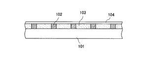
図8に、本発明の光学素子の一実施形態であるカラーフィルタの一例の断面を模式的に示す。図中、101は支持基板としての透明基板、102は隔壁を兼ねたブラックマトリクス、103は画素である着色部、104は必要に応じて形成される保護層である。本発明のカラーフィルタを用いて液晶素子を構成する場合には、着色部103上或いは、着色部103上に保護層104を形成したさらにその上に、液晶を駆動するためのITO(インジウム・チン・オキサイド)等透明導電材からなる透明導電膜が形成されて提供される場合もある。
【0038】
図9に、図8のカラーフィルタを用いて構成された、本発明の液晶素子の一実施形態の断面模式図を示す。図中、107は共通電極(透明導電膜)、108は配向膜、109は液晶、111は対向基板、112は画素電極、113は配向膜であり、図8と同じ部材には同じ符号を付して説明を省略する。
【0039】
カラー液晶素子は、一般的にカラーフィルタ側の基板101と対向基板111とを合わせ込み、液晶109を封入することにより形成される。液晶素子の一方の基板111の内側に、TFT(不図示)と画素電極112がマトリクス状に形成されている。また、カラーフィルタ側の基板101の内側には、画素電極112に対向する位置に、R、G、Bが配列するように、カラーフィルタの着色部103が形成され、その上に透明な共通電極107が形成される。さらに、両基板の面内には配向膜108,113が形成されており、液晶分子を一定方向に配列させている。これらの基板は、スペーサー(不図示)を介して対向配置され、シール材(不図示)によって貼り合わされ、その間隙に液晶109が充填される。
【0040】
上記液晶素子は、透過型の場合には、基板111及び画素電極112を透明素材で形成し、それぞれの基板の外側に偏光板を接着し、一般的に蛍光灯と散乱板を組み合わせたバックライトを用い、液晶化合物をバックライトの光の透過率を変化させる光シャッターとして機能させることにより表示を行う。また、反射型の場合には、基板111或いは画素電極112を反射機能を備えた素材で形成するか、或いは、基板111上に反射層を設け、透明基板101の外側に偏光板を設け、カラーフィルタ側から入射した光を反射して表示を行う。
【0041】
また、図7に、本発明の光学素子の他の実施形態である、有機エレクトロルミネッセンス素子(以下、「EL素子」と記す)の一例の断面模式図を示す。図中、91は支持基板である駆動基板、92は隔壁、93は画素である発光層、94は透明電極、96は金属層である。この図では、簡略化のために一つの画素領域のみを示している。
【0042】
駆動基板91には、TFT(不図示)、配線膜及び絶縁膜等が多層に積層されており、金属層96及び発光層93毎に配置した透明電極94間に発光層単位で電圧を印加可能に構成されている。駆動基板91は公知の薄膜プロセスによって製造される。
【0043】
本発明の有機EL素子の構造については、少なくとも一方が透明または半透明である一対の陽極及び陰極からなる電極間に、樹脂組成物からなる隔壁内に少なくとも発光材料を充填されてなる構成であれば、特に制限はなく、その構造は公知のものを採用することができ、また本発明の主旨を逸脱しない限りにおいて各種の改変を加えることができる。
【0044】
その積層構造は、例えば、
(1)電極(陰極)/発光層/正孔注入層/電極(陽極)
(2)電極(陽極)/発光層/電子注入層/電極(陰極)
(3)電極(陽極)/正孔注入層/発光層/電子注入層/電極(陰極)
(4)電極(陽極または陰極)/発光層/電極(陰極または陽極)
があるが、本発明は上記のいずれの構成の有機化合物層を設けた積層構造体を有するEL素子に対しても適用することができる。
【0045】
上記(1)は2層構造、(3)は3層構造、(4)は単層構造と称されるものである。本発明の有機EL素子はこれらの積層構造を基本とするが、これら以外の(1)から(4)を組み合わせた構造やそれぞれの層を複数有していてもよい。また、カラーフィルタと組み合わせることによって、フルカラー表示を実現しても良い。これらの積層構造からなる本発明の有機EL素子の形状、大きさ、材質、製造方法等は該有機EL素子の用途等に応じて適宜選択され、これらについては特に制限はない。
【0046】
本発明の有機EL素子の発光層に用いられる発光材料は特に限定されず、種々のものを適用することができる。具体的には、低分子蛍光体や高分子蛍光体が好ましく、高分子蛍光体がさらに好ましい。
【0047】
例えば、低分子有機化合物としては、特に限定はないが、ナフタレン及びその誘導体、アントラセン及びその誘導体、ペリレン及びその誘導体、ポリメチン系、キサンテン系、クマリン系、シアニン系などの色素類、8−ヒドロキシキノリン及びその誘導体の金属錯体、芳香族アミン、テトラフェニルシクロペンタジエン及びその誘導体、テトラフェニルブタジエン及びその誘導体等を用いることができる。具体的には、例えば、特開昭57−51781号、特開昭59−194393号公報に記載されているもの等、公知のものが使用可能である。
【0048】
また、発光材料として使用可能な高分子有機化合物としては、特に限定はないが、ポリフェニレンビニレン、ポリアリレン、ポリアルキルチオフェン、ポリアルキルフルオレン等を挙げることができる。
【0049】
尚、本発明の有機EL素子に用いる高分子蛍光体は、ランダム、ブロックまたはグラフト共重合体であってもよいし、それらの中間的な構造を有する高分子、例えばブロック性を帯びたランダム共重合体であってもよい。蛍光の量子収率の高い高分子蛍光体を得る観点からは完全なランダム共重合体よりブロック性を帯びたランダム共重合体やブロックまたはグラフト共重合体が好ましい。また本発明の有機EL素子は、薄膜からの発光を利用するので該高分子蛍光体は、固体状態で蛍光を有するものが用いられる。
【0050】
該高分子蛍光体に対する良溶媒としては、クロロホルム、塩化メチレン、ジクロロエタン、テトラヒドロフラン、トルエン、キシレンなどが例示される。高分子蛍光体の構造や分子量にもよるが、通常はこれらの溶媒に0.1重量%以上溶解させることができる。
【0051】
本発明の有機EL素子において、発光材料を含む層と陰極との間にさらに電子輸送層を設ける場合の電子輸送層中に使用する、或いは正孔輸送材料及び発光材料と混合使用する電子輸送性材料は、陰極より注入された電子を発光材料に伝達する機能を有している。このような電子輸送性材料について特に制限はなく、従来公知の化合物の中から任意のものを選択して用いることができる。
【0052】
該電子輸送性材料の好ましい例としては、ニトロ置換フルオレノン誘導体、アントラキノジメタン誘導体、ジフェニルキノン誘導体、チオピランジオキシド誘導体、複素環テトラカルボン酸無水物、或いはカルボジイミド等を挙げることができる。
【0053】
さらに、フレオレニリデンメタン誘導体、アントラキノジメタン誘導体及びアントロン誘導体、オキサジアゾール誘導体等を挙げることができる。また、発光層を形成する材料として開示されているが、8−ヒドロキシキノリン及びその誘導体の金属錯体等も電子輸送材料として用いることができる。
【0054】
次に、本発明の一例である積層構造を有する有機EL素子の代表的な作製方法について述べる。陽極及び陰極からなる一対の電極で、透明または半透明な電極としては、例えば、透明ガラス、透明プラスチック等の透明基板の上に、透明または半透明の電極を形成したものが用いられる。
【0055】
本発明のEL素子において、発光層は一般には適当な結着性樹脂と組み合わせて薄膜を形成する。上記結着剤としては広範囲な結着性樹脂より選択でき、例えばポリビニルカルバゾール樹脂、ポリカーボネート樹脂、ポリエステル樹脂、ポリアリレート樹脂、ブチラール樹脂、ポリスチレン樹脂、ポリビニルアセタール樹脂、ジアリルフタレート樹脂、アクリル樹脂、メタクリル樹脂、フェノール樹脂、エポキシ樹脂、シリコーン樹脂、ポリスルホン樹脂、尿素樹脂等が挙げられるが、これらに限定されるものではない。これらは単独または共重合体ポリマーとして1種または2種以上混合して用いても良い。陽極材料としては仕事関数がなるべく大きなものが良く、例えば、ニッケル、金、白金、パラジウム、セレン、レニウム、イリジウムやこれらの合金、或いは酸化錫、酸化錫インジウム(ITO)、ヨウ化銅が好ましい。またポリ(3−メチルチオフェン)、ポリフェニレンスルフィド或いはポリピロール等の導電性ポリマーも使用出来る。
【0056】
一方、陰極材料としては仕事関数が小さな銀、鉛、錫、マグネシウム、アルミニウム、カルシウム、マンガン、インジウム、クロム或いはこれらの合金が用いられる。
【0057】
以下に、図面を参照して本発明の光学素子の製造方法について説明する。
【0058】
図1、図2は本発明の光学素子の製造方法を模式的に示す工程図である。以下に各工程について説明する。尚、以下の工程(a)〜(h)は図1、図2の(a)〜(h)に対応する。また、図1、図2の各工程において紙面左側の(a−1)〜(h−1)は上方より見た平面模式図、紙面右側の(a−2)〜(h−2)は(a−1)〜(h−1)のA−B断面模式図である。図中、1は支持基板、3は隔壁、4は隔壁3の開口部、5はレジストパターン、6はインクジェットヘッド、7はインク、8は画素、9は隔壁3を形成する樹脂組成物である。
【0059】
工程(a)
支持基板1を用意する。支持基板1は、図8に例示したカラーフィルタを製造する場合には透明基板101であり、一般にはガラス基板が用いられるが、液晶素子を構成する目的においては、所望の透明性、機械的強度等の必要特性を有するものであれば、プラスチック基板なども用いることができる。
【0060】
また、図7に例示したEL素子を製造する場合には、支持基板1は透明電極94を形成した駆動基板91であり、図7の如く当該基板側から発光を観察する場合には、駆動基板91にガラス基板などの透明基板を用いる。
【0061】
該支持基板1には、予め親インク化処理を施しておくことが望ましい。親インク化処理としては、例えばアルカリ水溶液による洗浄処理、UV洗浄処理、エキシマ洗浄処理、コロナ放電処理、酸素プラズマ処理等の方法が好適に用いられる。
【0062】
工程(b)
支持基板1上に、隔壁3をパターン形成するため、及び、後述する隔壁3上面のフッ素化処理において隔壁3の側面と支持基板1表面とを保護するためのレジストパターン5を形成する。レジストとしては、フッ素化処理後に除去しうる材料を用いる必要がある。当該レジストパターン5の形成方法としては、感光性レジストを所定パターンのマスクを介して露光、現像するフォトリソグラフィ法や、感光性もしくは非感光性材料を印刷或いはインクジェット法で直接パターン形成する方法、さらには、感光性レジストを介して非感光性材料をパターニングするリフトオフ法などが適用できるが、これらの方法に限定されるものではない。しかしながら、パターン解像度や容易さを加味して、フォトリソグラフィ法、さらには、光分解型のポジ型レジストを用いる方法が好ましい。特に、アルカリ可溶のポジ型レジストを用いた場合、該レジスト除去時のアルカリ洗浄によって、支持基板表面が親インク化されるため、インク付与時の濡れ性が高くなり、白抜け防止効果がより高まり、好ましい。
【0063】
工程(c)
好ましくは、レジストパターン5にフッ素化処理を施す。当該処理によって、レジストパターン5の表面は撥インク性を増大し、後述する工程においてインクジェットヘッドより樹脂組成物9をインクとしてレジストパターン5の間隙に付与して隔壁3を形成する際に、隔壁3の線幅よりも大きな液滴の樹脂組成物9を受けても、レジストパターン5表面の撥インク性によって間隙に樹脂組成物が速やかに流れ込むため、インクジェット方式においても解像度の高い隔壁パターンを形成することができる。
【0064】
当該フッ素化処理としては、工程が簡単でありレジストパターン5表面を良好にフッ素化して撥インク性を増大させることができる方法として、少なくともフッ素原子を含有するガスを導入してプラズマ照射を行うプラズマ処理が好ましく用いられる。
【0065】
当該工程において用いられる、少なくともフッ素原子を含有するガスとしては、CF4、CHF3、C2F6、SF6、C3F8、C5F8から選択されるハロゲンガスを1種以上用いることが好ましい。特に、C5F8(オクタフルオロシクロペンテン)は、オゾン破壊能が0であると同時に、大気寿命が従来のガスに比べて(CF4:5万年、C4F8:3200年)0.98年と非常に短い。従って、地球温暖化係数が90(CO2=2とした100年積算値)と、従来のガスに比べて(CF4:6500、C4F8:8700)非常に小さく、オゾン層や地球環境保護に極めて有効であり、本発明で使用する上で望ましい。
【0066】
さらに、導入ガスとしては、必要に応じて酸素、アルゴン、ヘリウム等のガスを併用しても良い。本工程においては、上記CF4、CHF3、C2F6、SF6、C3F8、C5F8から選択されるハロゲンガスを1種以上とO2との混合ガスを用いると、本工程においてフッ素化処理されるレジストパターン5表面の撥インク性の程度を制御することが可能になる。但し、当該混合ガスにおいて、O2の混合比率が30%を超えるとO2による酸化反応が支配的になり、撥インク性向上効果が妨げられるため、また、O2混合比率が30%を超えると樹脂に対するダメージが顕著になるため、当該混合ガスを用いる場合にはO2の混合比率が30%以下の範囲で使用する必要がある。
【0067】
また、プラズマの発生方法としては、低周波放電、高周波放電、マイクロ波放電等の方式を用いることができ、プラズマ処理の際の圧力、ガス流量、放電周波数、処理時間等の条件は任意に設定することができる。
【0068】
図5、図6に、上記プラズマ処理工程に用いることが可能なプラズマ発生装置の模式図を示す。図中、51は上部電極、52は下部電極、53は被処理基板、54は高周波電極である。当該装置は平行平板の2極電極に高周波電圧を印加して、プラズマを発生させる。図5はカソードカップリング方式、図6はアノードカップリング方式の装置を示し、どちらの方式においても、圧力、ガス流量、放電周波数、処理時間等の条件によって、レジストパターン5表面の撥インク性を所望の程度とすることができる。
【0069】
図5、図6に示したプラズマ発生装置において、図5のカソードカップリング方式は処理時間を短くすることが可能であり、当該処理工程に有利である。また、図6のアノードカップリング方式では、必要以上に支持基板1にダメージを与えることがない点で有利である。よって、本工程に用いるプラズマ発生装置は、支持基板1やレジストパターン5の材料に応じて選択すればよい。
【0070】
工程(d)
インクジェットヘッド6より、樹脂組成物9をレジストパターン5の形成されていない領域(間隙)に付与して隔壁3を形成する。インクジェットとしては、エネルギー発生素子として電気熱変換体を用いたバブルジェットタイプ、或いは圧電素子を用いたピエゾジェットタイプ等が使用可能である。
【0071】
本発明においては、当該工程においてインクジェット方式を用いることにより、樹脂組成物9はレジストパターン5の間隙に選択的に付与されるため、レジストパターン5の少なくとも一部を露出させておくことができ、一般的なリフトオフ法のように全面を樹脂組成物9で覆ってしまう場合に比べて、後工程におけるレジストパターン5の除去が容易になる。また、レジストパターン5上に樹脂組成物9がのってしまった場合でも、レジストパターン5の除去と同時に該樹脂組成物9も除去されるため、隔壁3のパターンには影響しない。
【0072】
本発明において、隔壁3を形成するために用いられる樹脂組成物としては、エポキシ系樹脂、アクリル系樹脂、ポリアミドイミドを含むポリイミド系樹脂、ウレタン系樹脂、ポリエステル系樹脂、ポリビニル系樹脂などの感光性または非感光性の樹脂材料を用いることができるが、250℃以上の耐熱性を有することが好ましく、その点から、エポキシ系樹脂、アクリル系樹脂、ポリイミド系樹脂が好ましく用いられる。
【0073】
また、かかる隔壁3を遮光層とする場合には、上記樹脂組成物9中に、遮光剤を分散せしめた黒色樹脂組成物を用いる。該遮光剤としては、後述するフッ素化処理によって隔壁3の上面により高い撥インク性が得られることから、カーボンブラックを用いることが望ましく、該カーボンブラックとしては、チャネルブラック、ローラーブラック、ディスクブラックと呼ばれているコンタクト法で製造されたもの、ガスファーネストブラック、オイルファーネストブラックと呼ばれているファーネスト法で製造されたもの、サーマルブラック、アセチレンブラックと呼ばれているサーマル法で製造されたものなどを用いることができるが、特に、チャネルブラック、ガスファーネストブラック、オイルファーネストブラックが好ましい。さらに必要に応じて、R、G、Bの顔料の混合物などを加えても良い。また、一般に市販されている黒色レジストを用いることもできる。必要に応じて高抵抗化した遮光層を用いても良い。
【0074】
工程(e)
レジストパターン5を支持基板1上に残したまま、フッ素化処理を施し、隔壁3の上面の撥インク性を増大させる。当該フッ素化処理は、先の工程(c)のフッ素化処理と同様であり、少なくともフッ素原子を含有するガスを導入してプラズマ照射を行うプラズマ処理が好ましく用いられる。該プラズマ処理の条件及び用いられる装置についても、先の工程(c)における説明と同様である。
【0075】
工程(f)
レジストパターン5を除去する。レジストの除去方法としては、用いられるレジストの材質に応じて異なるが、隔壁3の密着性、フッ素化処理された隔壁3上面の撥インク性に悪影響を与えない方法を用いる必要がある。例えば、アルカリ水溶液や有機溶剤により溶解する方法や、それに加えて紫外線エネルギー照射を併用する方法がある。
【0076】
工程(g)
インクジェット記録装置を用いて、インクジェットヘッド6より、インク7を隔壁3で囲まれた領域(開口部4)に付与する。インクジェットとしては、エネルギー発生素子として電気熱変換体を用いたバブルジェットタイプ、或いは圧電素子を用いたピエゾジェットタイプ等が使用可能である。また、インク7としては、カラーフィルタの場合には硬化後にR、G、Bの着色部を形成するように各色の着色剤を含むもの、EL素子の場合には、硬化後に電圧印加によって発光する発光層を形成する材料を用いる。いずれの場合も、インク7は硬化成分、水、溶剤を少なくとも含むものが好ましい。以下に、本発明の製造方法によってカラーフィルタを製造する場合に用いるインクの組成についてさらに詳細に説明する。
【0077】
〔1〕着色剤
本発明でインク中に含有させる着色剤としては、染料系及び顔料系共に使用可能であるが、顔料を使用する場合には、インク中で均一に分散させるために別途分散剤の添加が必要となり、全固形分中の着色剤比率が低くなってしまうことから、染料系の着色剤が好ましく用いられる。また、着色剤の添加量としては、後述する硬化成分と同量以下であることが好ましい。
【0078】
〔2〕硬化成分
後工程におけるプロセス耐性、信頼性等を考慮した場合、熱処理或いは光照射等の処理により硬化し、着色剤を固定化する成分、即ち架橋可能なモノマー或いはポリマー等の成分を含有することが好ましい。特に、後工程における耐熱性を考慮した場合、硬化可能な樹脂組成物を用いることが好ましい。具体的には、例えば基材樹脂として、水酸基、カルボキシル基、アルコキシ基、アミド基等の官能基を有するアクリル樹脂、シリコーン樹脂;またはヒドロキシプロピルセルロース、ヒドロキシエチルセルロース、メチルセルロース、カルボキシメチルセルロース等のセルロース誘導体或いはそれらの変性物;またはポリビニルピロリドン、ポリビニルアルコール、ポリビニルアセタール等のビニル系ポリマーが挙げられる。さらに、これらの基材樹脂を光照射或いは加熱処理により硬化させるための架橋剤、光開始剤を用いることが可能である。具体的には、架橋剤としては、メチロール化メラミン等のメラミン誘導体が、また光開始剤としては重クロム酸塩、ビスアジド化合物、ラジカル系開始剤、カチオン系開始剤、アニオン系開始剤等が使用可能である。また、これらの光開始剤を複数種混合して、或いは他の増感剤と組み合わせて使用することもできる。
【0079】
〔3〕溶剤
本発明で使用されるインクの媒体としては、水及び有機溶剤の混合溶媒が好ましく使用される。水としては種々のイオンを含有する一般の水ではなく、イオン交換水(脱イオン水)を使用することが好ましい。
【0080】
有機溶剤としては、メチルアルコール、エチルアルコール、n−プロピルアルコール、イソプロピルアルコール、n−ブチルアルコール、sec−ブチルアルコール、tert−ブチルアルコール等の炭素数1〜4のアルキルアルコール類;ジメチルホルムアミド、ジメチルアセトアミド等のアミド類;アセトン、ジアセトンアルコール等のケトン類またはケトアルコール類;テトラヒドロフラン、ジオキサン等のエーテル類;ポリエチレングリコール、ポリプロピレングリコール等のポリアルキレングリコール類;エチレングリコール、プロピレングリコール、ブチレングリコール、トリエチレングリコール、チオジグリコール、へキシレングリコール、ジエチレングリコール等のアルキレン基が2〜4個の炭素を含有するアルキレングリコール類;グリセリン類;エチレングリコールモノメチルエーテル、ジエチレングリコールメチルエーテル、トリエチレングリコールモノメチルエーテル等の多価アルコールの低級アルキルエーテル類;N−メチル−2−ピロリドン、2−ピロリドン等の中から選択することが好ましい。
【0081】
また、上記成分の他に、必要に応じて所望の物性値を持つインクとするために、沸点の異なる2種類以上の有機溶剤を混合して用いたり、界面活性剤、消泡剤、防腐剤等を添加しても良い。
【0082】
工程(h)
熱処理、光照射等必要な処理を施し、インク7中の溶剤成分を除去して硬化させることにより、画素8を形成する。
【0083】
さらに、カラーフィルタの場合には、前記したように、必要に応じて保護層や透明導電膜を形成する。この場合の保護層としては、光硬化タイプ、熱硬化タイプ、或いは光熱併用硬化タイプの樹脂材料、或いは、蒸着、スパッタ等によって形成された無機膜等を用いることができ、カラーフィルタとした場合の透明性を有し、その後の透明導電膜形成プロセス、配向膜形成プロセス等に耐えうるものであれば使用可能である。また、透明導電膜は、保護層を介さずに着色部上に直接形成しても良い。また、EL素子の場合には、金属層等必要な部材を画素上に形成する。
【0084】
【実施例】
(参考実施例1)
〔レジストパターンの形成〕ガラス基板(コーニング製「1737」)上に、ポジ型レジスト(ヘキスト製「AZ−4903」)をスピンコートにより塗布し、所定の露光、現像処理を行って、膜厚10μm、75μm×225μmの長方形のレジストが20μmの間隔をおいて縦横に複数個配列されたレジストパターンを得た。
【0085】
〔ブラックマトリクス(隔壁)の形成〕
吐出量40plのインクジェットヘッドを具備するインクジェット記録装置を用いて、上記レジストパターンの間隙に黒色レジスト(新日鉄化学製「V−259BK」)を乾燥時膜厚2μmとなるように充填した。その後、90℃のホットプレート上で2分間加熱して黒色レジストを指触乾燥状態とし、次いで紫外線の全面露光により該黒色レジストに光硬化を施してブラックマトリクスを形成すると同時に、レジストパターンを光分解した。
【0086】
〔ブラックマトリクスのフッ素化処理〕
上記ブラックマトリクスを形成したガラス基板(ブラックマトリクス基板)に、平行平板型のプラズマ処理装置を用いて、以下の条件にてプラズマ処理を施した。
【0087】
使用ガス :CF4
ガス流量 :80sccm
圧力 :8Pa
RFパワー :150W
処理時間 :60sec
【0088】
〔レジストパターンの除去〕
上記プラズマ処理を施したブラックマトリクス基板を水酸化ナトリウム水溶液(pH11)で処理し、レジストパターンを除去した。次に十分に水洗し、水切りを経て230℃のオーブン中で30分間加熱し、ブラックマトリクスを完全に硬化させた。
【0089】
〔ブラックマトリクス基板の撥インク性の評価〕
得られたブラックマトリクス基板の純水に対する接触角を測定したところ、
ブラックマトリクス上面:118°
ガラス基板表面:17°
であった。
【0090】
〔インクの調整〕
下記に示す組成からなるアクリル系共重合体を熱硬化成分として用い、以下の組成にてR、G、Bの各インクを調製した。
【0091】
硬化成分
メチルメタクリレート 50重量部
ヒドロキシエチルメタクリレート 30重量部
N−メチロールアクリルアミド 20重量部
【0092】
Rインク
C.I.アシッドオレンジ148 3.5重量部
C.I.アシッドレッド289 0.5重量部
ジエチレングリコール 30重量部
エチレングリコール 20重量部
イオン交換水 40重量部
上記硬化成分 6重量部
【0093】
Gインク
C.I.アシッドイエロー23 2重量部
亜鉛フタロシアニンスルホアミド 2重量部
ジエチレングリコール 30重量部
エチレングリコール 20重量部
イオン交換水 40重量部
上記硬化成分 6重量部
【0094】
Bインク
C.I.ダイレクトブルー199 4重量部
ジエチレングリコール 30重量部
エチレングリコール 20重量部
イオン交換水 40重量部
上記硬化成分 6重量部
【0095】
〔着色部の作製〕
吐出量20plのインクジェットヘッドを具備したインクジェット記録装置を用い、上記ブラックマトリクス基板に対して、上記R、G、Bインクを開口部1個あたり200〜800plの範囲で100plおきに量を変化させて付与した。次いで、90℃で10分間、引き続き230℃で30分間の熱処理を行ってインクを硬化させて着色部(画素)とし、インク付与量の異なる7種類のカラーフィルタを作製した。
【0096】
〔混色及び白抜けの評価〕
得られたカラーフィルタを光学顕微鏡で観察したところ、全てのカラーフィルタにおいて、混色、白抜けは観察されなかった。また、このカラーフィルタに保護層、透明導電膜を設けて構成した液晶素子は、良好な表示品質であった。
【0097】
(参考実施例2)
レジストパターンを光硬化型ネガレジスト(三洋化成製「PVP−レジスト」)を用いて膜厚6μmとなるように形成し、該レジストの除去にアルカリ水溶液(東京応化製「NMD−3」)を用いた以外は参考実施例1と同様にしてカラーフィルタを作製した。尚、樹脂組成物充填時にレジストパターンに樹脂組成物が一部かかった部分が生じたが、レジスト除去時に除去された。
【0098】
〔ブラックマトリクス基板の撥インク性の評価〕
得られたブラックマトリクス基板の純水に対する接触角を測定したところ、
ブラックマトリクス上面:115°
ガラス基板表面:11°
であった。
【0099】
〔混色及び白抜けの評価〕
得られたカラーフィルタを光学顕微鏡で観察したところ、全てのカラーフィルタにおいて、混色、白抜けは観察されなかった。
【0100】
(参考実施例3)
レジストパターンを、モノメタクリレート樹脂(親中村化学製「NKエステルSA」)を用いて凹版オフセット印刷により直接パターン形成し、膜厚が4μmとなるように形成し、このレジストの除去に水酸化ナトリウム水溶液を用いた以外は参考実施例1と同様にしてカラーフィルタを作製した。尚、樹脂組成物充填時にレジストパターン上にも樹脂組成物がのってしまった部分を生じたが、レジスト除去時に除去された。
【0101】
〔ブラックマトリクス基板の撥インク性の評価〕
得られたブラックマトリクス基板の純水に対する接触角を測定したところ、
ブラックマトリクス上面:128°
ガラス基板表面:13°
であった。
【0102】
〔混色及び白抜けの評価〕
得られたカラーフィルタを光学顕微鏡で観察したところ、全てのカラーフィルタにおいて、混色、白抜けは観察されなかった。
【0103】
(比較例1)
レジストパターンを形成せずに直接ガラス基板上にブラックマトリクスパターンを形成した。パターンとして幅20μm、高さ2μmと設定したが、線幅が60〜70μmとなってしまい、設計通りのブラックマトリクスが形成されなかった。
【0104】
(比較例2)
ブラックマトリクスのフッ素化処理を行わない以外は参考実施例1と同様にしてカラーフィルタを作製した。
【0105】
〔ブラックマトリクス基板の撥インク性の評価〕
得られたブラックマトリクス基板の純水に対する接触角を測定したところ、
ブラックマトリクス上面:76°
ガラス基板表面:65°
であった。
【0106】
〔混色及び白抜けの評価〕
得られたカラーフィルタを光学顕微鏡で観察したところ、全てのカラーフィルタにおいて、白抜けが観察され、インク付与量が300pl以上のカラーフィルタにおいて混色が確認された。
【0107】
(実施例4)
レジストパターンの膜厚を5μmとし、レジストパターンに対して以下の条件でプラズマ処理を施した以外は参考実施例1と同様にしてカラーフィルタを作製した。
【0108】
〔レジストパターンのフッ素化処理〕
使用ガス :CF4
ガス流量 :80sccm
圧力 :8Pa
RFパワー :150W
処理時間 :60sec
【0109】
〔レジストパターン基板の撥インク性の評価〕
フッ素化処理の後レジストパターン基板の純水に対する接触角を測定したところ、
レジストパターン上面:105°
ガラス基板表面:13°
であった。
【0110】
〔ブラックマトリクス基板の撥インク性の評価〕
得られたブラックマトリクス基板の純水に対する接触角を測定したところ、
ブラックマトリクス上面:118°
ガラス基板表面:17°
であった。
【0111】
〔混色及び白抜けの評価〕
得られたカラーフィルタを光学顕微鏡で観察したところ、全てのカラーフィルタにおいて、混色、白抜けは観察されなかった。
【0112】
(参考実施例5)
レジストパターンを光硬化型ネガレジスト(三洋化成製「PVP−レジスト」)を用いて膜厚5μmとなるように形成し、該レジストの除去にアルカリ水溶液(東京応化製「NMD−3」)を用いた以外は実施例4と同様にしてカラーフィルタを作製した。
【0113】
〔レジストパターン基板の撥インク性の評価〕
フッ素化処理の後レジストパターン基板の純水に対する接触角を測定したところ、
レジストパターン上面:100°
ガラス基板表面:15°
であった。
【0114】
〔ブラックマトリクス基板の撥インク性の評価〕
得られたブラックマトリクス基板の純水に対する接触角を測定したところ、
ブラックマトリクス上面:110°
ガラス基板表面:10°
であった。
【0115】
〔混色及び白抜けの評価〕
得られたカラーフィルタを光学顕微鏡で観察したところ、全てのカラーフィルタにおいて、混色、白抜けは観察されなかった。
【0116】
(比較例3)
レジストパターンのフッ素化処理、及び、ブラックマトリクスのフッ素化処理を行わない以外は実施例4と同様にしてカラーフィルタを作製した。
【0117】
〔レジストパターン基板の撥インク性の評価〕
パターニング後レジストパターン基板の純水に対する接触角を測定したところ、
レジストパターン上面:74°
ガラス基板表面:63°
であった。
【0118】
〔ブラックマトリクス基板の撥インク性の評価〕
得られたブラックマトリクス基板の純水に対する接触角を測定したところ、
ブラックマトリクス上面:73°
ガラス基板表面:62°
であった。
【0119】
〔混色及び白抜けの評価〕
得られたカラーフィルタを光学顕微鏡で観察したところ、全てのカラーフィルタにおいて、白抜けは観察された。また、インク付与量が300pl以上のカラーフィルタにおいて混色が確認された。
【0120】
(参考実施例6)
薄膜プロセスによって形成された、配線膜及び絶縁膜等が多層に積層されてなるTFT駆動基板上に画素(発光層)単位に、透明電極としてITOをスパッタリングにより厚さ40nmになるように形成し、フォトリソ法により、画素形状に従ってパターニングを行った基板を用い、参考実施例1と同様にしてレジストパターンの除去まで行った。
【0121】
〔ブラックマトリクス基板の撥インク性の評価〕
得られたブラックマトリクス基板の純水に対する接触角を測定したところ、
ブラックマトリクス上面:122°
ガラス基板表面:15°
であった。
【0122】
〔インクの調整〕
電子輸送性2,5−ビス(5−tert−ブチル−2−ベンゾオキサゾルイル)−チオフェン〔蛍光ピーク450nmをもつ電子輸送性青色発光色素であり、発光中心形成化合物の1つである。以下、「BBOT」と記す〕30重量%を、ポリ−N−ビニルカルバゾール〔分子量150,000、関東化学社製、以下、「PVK」と記す〕よりなるホール輸送性ホスト化合物中に分子分散させることができるよう、両者をジクロロエタン溶液に溶解させた。該PVK−BBOTのジクロロエタン溶液にさらに、もう1つの発光中心形成化合物であるナイルレッドを0.015モル%となるように溶解し、インクを調整した。
【0123】
〔画素(発光層)の作成〕
インクジェット法により透明樹脂で囲まれた隔壁内に上記インクを充填、乾燥し、厚さ200nmの発光層を形成した。
【0124】
〔混色および白抜けの評価〕
各画素(発光層)は独立し、隔壁間で前記発光材料を含む溶液が隣接画素で混ざることはなかった。また、(白)抜けは確認されなかった。
【0125】
さらにこの上に、Mg:Ag(10:1)を真空蒸着させて厚さ200nmのMg:Ag陰極を作った。このようにして作ったEL素子の各画素に18Vの電圧を印加したところ、480cd/m2の均一な白色発光が得られた。
【0126】
【発明の効果】
以上説明したように、本発明によれば、混色や白抜けのない画素を備えた信頼性の高い光学素子をインクジェット方式により簡易なプロセスによって歩留まり良く製造することができ、着色部内で濃度ムラのないカラーフィルタ、発光層内で発光輝度ムラのないEL素子を歩留まり良く提供することができる。よって、上記カラーフィルタを用いて、カラー表示特性に優れた液晶素子をより安価に提供することができる。
【図面の簡単な説明】
【図1】本発明の光学素子の製造方法の一実施形態の工程図である。
【図2】本発明の光学素子の製造方法の一実施形態の工程図である。
【図3】インクジェット方式による光学素子の製造方法において発生する混色の概念図である。
【図4】インクジェット方式による光学素子の製造方法において発生する白抜けの概念図である。
【図5】本発明の製造方法において用いうるプラズマ発生装置の構成の一例を示す模式図である。
【図6】本発明の製造方法において用いうるプラズマ発生装置の他の構成を示す模式図である。
【図7】本発明の光学素子の一実施形態であるエレクトロルミネッセンス素子の一例の断面模式図である。
【図8】本発明の光学素子の他の実施形態であるカラーフィルタの一例の断面模式図である。
【図9】本発明の液晶素子の一実施形態の断面模式図である。
【符号の説明】
1 支持基板
3 隔壁
4 開口部
5 レジストパターン
6 インクジェットヘッド
7 インク
8 画素
9 樹脂組成物
31 透明基板
33 ブラックマトリクス
36 インク
38 白抜け
51 上部電極
52 下部電極
53 被処理基板
54 高周波電極
91 駆動基板
92 隔壁
93 発光層
94 透明電極
96 金属層
101 透明基板
102 ブラックマトリクス
103 着色部
104 保護層
107 共通電極
108 配向膜
109 液晶
111 対向基板
112 画素電極
113 配向膜[0001]
BACKGROUND OF THE INVENTION
The present invention uses an ink jet system for an optical element such as a color filter, which is a constituent member of a color liquid crystal element used in a color television, a personal computer, or a pachinko game machine, and an electroluminescence element having a plurality of light emitting layers. In addition, the present invention relates to an optical element manufactured by the manufacturing method and a liquid crystal element using a color filter which is one of the optical elements.
[0002]
[Prior art]
In recent years, with the development of personal computers, especially portable personal computers, the demand for liquid crystal displays, particularly color liquid crystal displays, has been increasing. However, cost reduction is necessary for further dissemination, and there is an increasing demand for cost reduction of color filters that are particularly heavy in terms of cost.
[0003]
Conventionally, various methods have been tried to meet the above-described requirements while satisfying the required characteristics of the color filter, but a method that satisfies all the required characteristics has not yet been established. Each method will be described below.
[0004]
The first method is a staining method. In the dyeing method, first, a water-soluble polymer material layer, which is a dyeing material, is formed on a transparent substrate, patterned into a desired shape by a photolithography process, and then the obtained pattern is immersed in a dyeing bath. To obtain a colored pattern. By repeating this step three times, a colored layer composed of three colored portions of R (red), G (green), and B (blue) is formed.
[0005]
The second method is a pigment dispersion method, which has been most actively performed in recent years. In this method, first, a photosensitive resin layer in which a pigment is dispersed is formed on a transparent substrate, and this is patterned to obtain a monochromatic pattern. By repeating this process three times, a colored layer composed of colored portions of R, G, and B is formed.
[0006]
There is an electrodeposition method as a third method. In this method, first, a transparent electrode is patterned on a transparent substrate, and immersed in an electrodeposition coating solution containing a pigment, a resin, an electrolytic solution, etc., and the first color is electrodeposited. This process is repeated three times to form a colored layer composed of three colored portions of R, G, and B, and finally fired.
[0007]
As a fourth method, a pigment is dispersed in a thermosetting resin, and printing is repeated three times to separate R, G, and B, and then the resin is thermally cured to form a colored layer. Is. In any method, a protective layer is generally formed on the colored layer.
[0008]
The point common to these methods is that it is necessary to repeat the same process three times in order to color the three colors of R, G, and B, resulting in high costs. Further, there is a problem that the yield decreases as the number of steps increases. Furthermore, in the electrodeposition method, the shape of the pattern that can be formed is limited, so that it is difficult to apply to the structure of a TFT type (active matrix driving method using a TFT, ie, a thin film transistor as a switching element) with the current technology. It is.
[0009]
Also, since the printing method has poor resolution, it is not suitable for forming a fine pitch pattern.
[0010]
In order to compensate for the above drawbacks, in recent years, a method for producing a color filter using an inkjet method has been actively studied. The method using the ink jet method has an advantage that the manufacturing process is simple and the cost is low.
[0011]
On the other hand, the ink jet method is not limited to the manufacture of color filters, but can also be applied to the manufacture of electroluminescent elements.
[0012]
An electroluminescence element has a structure in which a thin film containing a fluorescent inorganic and organic compound is sandwiched between a cathode and an anode, and excitons are obtained by injecting electrons and holes into the thin film and recombining them. Is generated by utilizing the emission of fluorescence when the exciton is deactivated. A fluorescent material used for such an electroluminescent element can be applied to a substrate on which an element such as a TFT is formed by an ink jet method to form a light emitting layer, whereby the element can be configured.
[0013]
[Problems to be solved by the invention]
As described above, since the ink jet system can simplify the manufacturing process and reduce the cost, it is applied to the manufacture of optical elements such as color filters and electroluminescent elements. However, in the manufacture of such an optical element, there are problems such as “color mixing” and “white spot” as problems peculiar to the ink jet system. Hereinafter, a case where a color filter is manufactured will be described as an example.
[0014]
“Mixed color” is a failure that occurs when ink is mixed between adjacent pixels (colored portions) of different colors. In the manufacturing method of the color filter in which the black matrix is used as a partition and ink is applied to the opening of the black matrix to form a colored portion, the volume is several to several tens of times the volume of the opening of the black matrix. It is necessary to apply an ink having When the solid content concentration of the colorant or the curing component contained in the ink is high, that is, when the volume of the applied ink is relatively small, the black matrix functions sufficiently as a partition wall, and the inside of the opening of the black matrix Since the ink can be held, the applied ink does not go over the black matrix and reach the colored portions of different colors adjacent to each other. However, when the solid concentration in the ink is low, that is, when it is necessary to apply a large amount of ink, the ink overflows beyond the black matrix serving as the partition wall, and color mixing occurs between adjacent colored portions. Resulting in. In particular, there is a limit to the viscosity of ink that can be stably ejected from the nozzles of an inkjet head, and there is also a limit to the concentration of solids contained in the ink, so a technique for avoiding color mixing is necessary. .
[0015]
In view of this, a method for preventing color mixing by utilizing a difference in wettability of ink between the colored portion and the partition wall has been proposed. For example, Japanese Patent Application Laid-Open No. 59-75205 proposes a method of forming a diffusion prevention pattern with a substance having poor wettability in order to prevent the ink from spreading outside the target area. Not disclosed. On the other hand, JP-A-4-123005 proposes a method of patterning a silicone rubber layer having a large water and oil repellency to form a partition wall for preventing color mixing. Further, JP-A-5-241011 and JP-A-5-241012 similarly disclose a method in which a silicone rubber layer is formed on a black matrix serving as a light shielding layer and used as a partition for preventing color mixing.
[0016]
According to these methods, even when an amount of ink far exceeding the height of the partition is applied, the surface layer of the partition shows ink repellency so that the ink is repelled, and the adjacent colored portion beyond the partition. Therefore, it is possible to effectively prevent color mixing.
[0017]
The conceptual diagram is shown in FIG. In the figure, 31 is a transparent substrate, 33 is a black matrix that also serves as a partition, and 36 is ink. When the upper surface of the
[0018]
In general, it is possible to obtain better ink repellency by using a fluorine compound than by using a silicon compound. For example, Japanese Patent Laid-Open No. 2000-35511 discloses a method of forming a positive resist pattern on a light shielding portion and further applying an ink repellent treatment agent on the pattern. The use of fluorine compounds is disclosed. However, in this method, it is necessary to remove the positive resist pattern provided on the light-shielding portion after forming the colored portion. However, when the resist pattern is removed, problems such as dissolution, peeling, and swelling of pixels may occur. is there.
[0019]
As a method for fluorinating the surface of the resin layer, Japanese Patent Application Laid-Open No. 6-65408 proposes a method in which a reaction gas of a fluorine compound is converted into plasma. Further, as an example in which this technique is applied to a color filter, in Japanese Patent Laid-Open No. 11-271753, the partition wall has a multilayer structure of a lower layer having affinity for ink and an upper layer having non-affinity, and the upper layer is used for ink. As a technique for making it non-affinity, a plasma treatment method using a gas containing a fluorine compound is disclosed.
[0020]
However, any of the above-described methods is to multi-layer the partition walls, and it is necessary to carry out the photolithography process a plurality of times. Therefore, there is a problem that the process is complicated, the cost is increased, and the yield is lowered.
[0021]
On the other hand, “blank” is a failure that occurs mainly because the applied ink cannot be sufficiently and uniformly diffused in the area surrounded by the partition walls, such as color unevenness and a decrease in contrast. It causes display failure.
[0022]
FIG. 4 shows a conceptual diagram of white spots. In the figure, the same members as those in FIG.
[0023]
In recent years, in the color filter for TFT type liquid crystal elements, the shape of the opening of the
[0024]
As a technique for solving such problems of color mixture and white spots, in Japanese Patent Application Laid-Open No. 9-203803, a region (concave portion) surrounded by a black matrix (convex portion) has a contact angle of 20 ° or less with respect to water. It has been proposed to use a substrate that has been subjected to ink-philic treatment so that Examples of methods for imparting ink affinity include water-soluble leveling agents and water-soluble surfactants. Furthermore, in order to solve the above-mentioned problem of color mixing at the same time, a technique for imparting ink repellency by treating the surface of the convex portion with an ink repellent treatment agent in advance has been disclosed. A method of coating with a fluorinated solvent using a silane coupling agent is exemplified. At this time, as a method for selectively repelling only the surface layer of the convex portion and not repelling the side surface of the convex portion,
(1) Two kinds of materials are laminated so that the convex part itself has such a property.
(2) Cover portions other than the convex portion with a resist, and apply an ink repellency treatment only to the upper surface of the convex portion. (3) Form a resist layer on the transparent substrate, and perform an ink repellency treatment on the entire surface, followed by a photolithography process. The method of patterning a resist layer by, for example, forming a convex part is illustrated.
[0025]
Similarly, Japanese Patent Application Laid-Open No. 9-230129 discloses a method of irradiating energy rays as a method of making a concave portion an ink-philic process. Also in this case, as a method of performing the ink repellent treatment only on the surface layer of the convex portion, a photosensitive material for forming the convex portion is applied on a glass substrate, and the entire surface is treated with an ink repellent treatment agent, and then photo A technique for patterning a photosensitive material by a lithography process is illustrated. Thereafter, the convex portion and the concave portion are simultaneously or selectively subjected to ink-inking treatment by irradiation with energy rays.
[0026]
However, since all of these methods perform the ink repellent treatment on the concave surface after the surface of the convex portion is subjected to the ink repellent treatment, the surface of the convex portion subjected to the ink repellent treatment when performing the ink remediation treatment. There is a problem that the ink repellency is lowered. Therefore, it is difficult to obtain sufficient ink affinity on the transparent substrate surface and the side surface of the black matrix, and sufficient ink repellency on the upper surface of the black matrix.
[0027]
The above problem also occurs when an electroluminescent element is manufactured by an ink jet method. That is, in an electroluminescence element, for example, when an organic semiconductor material that emits R, G, and B light is used as an ink, and the ink is applied to a region surrounded by a partition wall to form a pixel (light emitting layer). When ink is mixed between adjacent light emitting layers, there arises a problem that the light emitting layer cannot emit light having a desired color and luminance. Even in the case of a single color light emitting layer, the amount of ink filled in the partition is made uniform, so when ink flows into adjacent pixels, the amount of ink becomes non-uniform, which is recognized as luminance unevenness, which is a problem. It becomes. Further, when the ink is not sufficiently diffused in the region surrounded by the partition walls, there is a problem that sufficient light emission luminance cannot be obtained at the boundary portion between the light emitting layer and the partition walls. In the following description, for the sake of convenience, even when an electroluminescent element is manufactured, the mixing of ink between adjacent light emitting layers is “mixed color”, and the light emission luminance due to the repulsion of ink at the boundary between the light emitting layer and the partition wall. The occurrence of unevenness is referred to as “white spots”.
[0028]
An object of the present invention is to solve the above problems and provide a highly reliable optical element with a high yield when an optical element such as a color filter or an electroluminescence element is manufactured at low cost by a simple process using an inkjet method. There is. Specifically, when ink is applied to the area surrounded by the partition walls, color mixing between adjacent pixels is prevented, and the ink is sufficiently diffused in the area so that pixels without white spots are formed. It is to form. A further object of the present invention is to provide a liquid crystal element excellent in color display characteristics at a lower cost by using the optical element obtained by the production method.
[0029]
[Means for Solving the Problems]
A first aspect of the present invention is a method for producing an optical element having at least a partition made of a resin composition located between a plurality of pixels and adjacent pixels on a support substrate,
Forming a resist pattern with an alkali-soluble positive resist in a region surrounded by a partition wall on a support substrate;
A step of subjecting the formed resist pattern to a fluorination treatment,
A step of forming a partition wall by applying a resin composition to the gap between the resist patterns subjected to the fluorination treatment by an inkjet method;
Applying a fluorination treatment to the upper surface of the partition wall while leaving the resist pattern;
Dissolving and removing the resist pattern with an alkaline aqueous solution ;
Forming a pixel by applying ink to a region surrounded by the partition wall by an inkjet method;
It is a manufacturing method of the optical element characterized by having.
[0030]
In the present invention, the fluorination treatment is a plasma treatment in which plasma irradiation is performed by introducing a gas containing at least fluorine atoms, the partition is formed of a resin composition containing a light shielding agent, it shielding agent is carbon black, at least the curing component is above Symbol ink, water, it contains an organic solvent, the resin composition is applied by an inkjet method in a gap between a resist pattern which has been subjected to the fluorination treatment, the photosensitive A preferable embodiment is that it contains a conductive resin, the ink contains a colorant, and a color filter in which the pixel is a colored portion is produced, and an electroluminescent element in which the pixel is a light emitting layer is produced. Is included.
[0033]
Further the second aspect of the present invention is a method of manufacturing a liquid crystal device ing by sandwiching a liquid crystal between a pair of substrates, as one substrate, an optical element manufactured by the manufacturing method of an optical element of the present invention It is a manufacturing method of the liquid crystal element characterized by using .
[0034]
DETAILED DESCRIPTION OF THE INVENTION
In the method for producing an optical element of the present invention, in the step of forming the partition wall on the support substrate, a resist pattern is formed on the support substrate, a resin composition is applied to the gap to form the partition wall, and fluorination treatment is performed. The resist pattern is removed after increasing the ink repellency of the upper surface of the partition wall, and ink is applied by an ink jet method to form a pixel. Therefore, in the present invention, when ink is applied, the ink repellency on the upper surface of the partition wall sufficiently retains even a large amount of ink to prevent color mixing, while the side walls of the partition wall and the surface of the support substrate have high ink affinity and promptly. Ink spreads and prevents white spots.
[0035]
In the present invention, the above “ink” is a generic term for, for example, optically and electrically functional liquids after being dried and cured, and is not limited to conventionally used coloring materials.
[0036]
Examples of the optical element of the present invention manufactured by the manufacturing method of the present invention include a color filter and an electroluminescence element. First, embodiments of the optical element of the present invention will be described.
[0037]
FIG. 8 schematically shows a cross section of an example of a color filter which is an embodiment of the optical element of the present invention. In the figure, 101 is a transparent substrate as a support substrate, 102 is a black matrix that also serves as a partition, 103 is a colored portion that is a pixel, and 104 is a protective layer that is formed as necessary. When a liquid crystal element is formed using the color filter of the present invention, ITO (indium tin oxide) for driving the liquid crystal is formed on the
[0038]
FIG. 9 is a schematic cross-sectional view of an embodiment of the liquid crystal element of the present invention, which is configured using the color filter of FIG. In the figure, 107 is a common electrode (transparent conductive film), 108 is an alignment film, 109 is a liquid crystal, 111 is a counter substrate, 112 is a pixel electrode, and 113 is an alignment film. Therefore, the description is omitted.
[0039]
A color liquid crystal element is generally formed by combining a
[0040]
When the liquid crystal element is a transmissive type, the
[0041]
FIG. 7 shows a schematic cross-sectional view of an example of an organic electroluminescence element (hereinafter referred to as “EL element”), which is another embodiment of the optical element of the present invention. In the figure, 91 is a drive substrate as a support substrate, 92 is a partition, 93 is a light emitting layer as a pixel, 94 is a transparent electrode, and 96 is a metal layer. In this figure, only one pixel region is shown for simplification.
[0042]
The driving
[0043]
The structure of the organic EL device of the present invention is such that at least one of a pair of anode and cathode that is transparent or translucent is filled with at least a light emitting material in a partition made of a resin composition. For example, there is no particular limitation, and a known structure can be adopted, and various modifications can be made without departing from the gist of the present invention.
[0044]
The laminated structure is, for example,
(1) Electrode (cathode) / light emitting layer / hole injection layer / electrode (anode)
(2) Electrode (anode) / light emitting layer / electron injection layer / electrode (cathode)
(3) Electrode (anode) / hole injection layer / light emitting layer / electron injection layer / electrode (cathode)
(4) Electrode (anode or cathode) / light emitting layer / electrode (cathode or anode)
However, the present invention can also be applied to an EL element having a stacked structure in which an organic compound layer having any one of the above structures is provided.
[0045]
(1) a two-layer structure, (3) is a three-layer structure, (4) is what is referred to as Tanso構granulation. The organic EL element of the present invention is based on these laminated structures, but may have a structure in which (1) to (4) other than these are combined, or a plurality of each layer. Further, a full color display may be realized by combining with a color filter. The shape, size, material, manufacturing method and the like of the organic EL element of the present invention having such a laminated structure are appropriately selected according to the use of the organic EL element, and there are no particular restrictions on these.
[0046]
The light emitting material used for the light emitting layer of the organic EL device of the present invention is not particularly limited, and various materials can be applied. Specifically, low molecular phosphors and polymer phosphors are preferable, and polymer phosphors are more preferable.
[0047]
For example, the low molecular organic compound is not particularly limited, but naphthalene and derivatives thereof, anthracene and derivatives thereof, perylene and derivatives thereof, polymethine-based, xanthene-based, coumarin-based, cyanine-based pigments, 8-hydroxyquinoline, and the like. And metal complexes of the derivatives thereof, aromatic amines, tetraphenylcyclopentadiene and derivatives thereof, tetraphenylbutadiene and derivatives thereof, and the like can be used. Specifically, for example, known ones such as those described in JP-A-57-51781 and JP-A-59-194393 can be used.
[0048]
In addition, the high molecular organic compound that can be used as the light emitting material is not particularly limited, and examples thereof include polyphenylene vinylene, polyarylene, polyalkylthiophene, and polyalkylfluorene.
[0049]
The polymeric fluorescent substance used in the organic EL device of the present invention may be a random, block or graft copolymer, or a polymer having an intermediate structure thereof, for example, a random copolymer having a block property. It may be a polymer. From the viewpoint of obtaining a polymeric fluorescent substance having a high fluorescence quantum yield, a random copolymer having a block property and a block or graft copolymer are preferable to a complete random copolymer. In addition, since the organic EL element of the present invention utilizes light emission from a thin film, the polymer fluorescent substance having fluorescence in a solid state is used.
[0050]
Examples of the good solvent for the polymeric fluorescent substance include chloroform, methylene chloride, dichloroethane, tetrahydrofuran, toluene, xylene and the like. Although depending on the structure and molecular weight of the polymeric fluorescent substance, it can usually be dissolved in these solvents in an amount of 0.1% by weight or more.
[0051]
In the organic EL device of the present invention, an electron transport property used in an electron transport layer when an electron transport layer is further provided between a layer containing a light emitting material and a cathode, or mixed with a hole transport material and a light emitting material. The material has a function of transmitting electrons injected from the cathode to the light emitting material. There is no restriction | limiting in particular about such an electron transport material, Arbitrary things can be selected and used from a conventionally well-known compound.
[0052]
Preferable examples of the electron transporting material include nitro-substituted fluorenone derivatives, anthraquinodimethane derivatives, diphenylquinone derivatives, thiopyran dioxide derivatives, heterocyclic tetracarboxylic acid anhydrides, and carbodiimides.
[0053]
Further examples include fluorenylidenemethane derivatives, anthraquinodimethane derivatives and anthrone derivatives, oxadiazole derivatives, and the like. Further, although disclosed as a material for forming a light-emitting layer, 8-hydroxyquinoline and metal complexes of derivatives thereof can also be used as an electron transporting material.
[0054]
Next, a typical method for manufacturing an organic EL element having a laminated structure as an example of the present invention will be described. As a pair of electrodes composed of an anode and a cathode, as a transparent or translucent electrode, for example, a transparent substrate such as transparent glass or transparent plastic on which a transparent or translucent electrode is formed is used.
[0055]
In the EL device of the present invention, the light emitting layer is generally combined with an appropriate binder resin to form a thin film. The binder can be selected from a wide range of binder resins such as polyvinyl carbazole resin, polycarbonate resin, polyester resin, polyarylate resin, butyral resin, polystyrene resin, polyvinyl acetal resin, diallyl phthalate resin, acrylic resin, methacrylic resin. , Phenol resin, epoxy resin, silicone resin, polysulfone resin, urea resin and the like, but are not limited thereto. These may be used alone or in combination as a copolymer polymer. As the anode material, a material having a work function as large as possible is preferable. For example, nickel, gold, platinum, palladium, selenium, rhenium, iridium and alloys thereof, or tin oxide, indium tin oxide (ITO), and copper iodide are preferable. In addition, conductive polymers such as poly (3-methylthiophene), polyphenylene sulfide, and polypyrrole can also be used.
[0056]
On the other hand, silver, lead, tin, magnesium, aluminum, calcium, manganese, indium, chromium, or alloys thereof having a small work function are used as the cathode material.
[0057]
Hereinafter, a method for producing an optical element of the present invention will be described with reference to the drawings.
[0058]
1 and 2 are process diagrams schematically showing a method for producing an optical element of the present invention. Each step will be described below. The following steps (a) to (h) correspond to (a) to (h) in FIGS. 1 and 2, (a-1) to (h-1) on the left side of the drawing are schematic plan views viewed from above, and (a-2) to (h-2) on the right side of the drawing are ( It is an AB cross-sectional schematic diagram of a-1)-(h-1). In the figure, 1 is a support substrate, 3 is a partition, 4 is an opening of the
[0059]
Step (a)
A
[0060]
When the EL element illustrated in FIG. 7 is manufactured, the
[0061]
The
[0062]
Step (b)
A resist
[0063]
Step (c)
Preferably, the resist
[0064]
As the fluorination treatment, a method in which the process is simple and the surface of the resist
[0065]
As the gas containing at least a fluorine atom used in the process, one or more halogen gases selected from CF 4 , CHF 3 , C 2 F 6 , SF 6 , C 3 F 8 , and C 5 F 8 are used. It is preferable. In particular, C 5 F 8 (octafluorocyclopentene) has an ozone depleting ability of 0, and at the same time, has an atmospheric lifetime (CF 4 : 50,000 years, C 4 F 8 : 3200) as compared with conventional gases. It is very short with 98 years. Therefore, the global warming potential is 90 (100-year integrated value with CO 2 = 2), which is very small (CF 4 : 6500, C 4 F 8 : 8700) compared to conventional gases, and the ozone layer and the global environment. It is extremely effective for protection and is desirable for use in the present invention.
[0066]
Further, as the introduced gas, a gas such as oxygen, argon, or helium may be used in combination as necessary. In this step, when a mixed gas of at least one halogen gas selected from CF 4 , CHF 3 , C 2 F 6 , SF 6 , C 3 F 8 , and C 5 F 8 and O 2 is used, In this step, the degree of ink repellency on the surface of the resist
[0067]
In addition, plasma generation methods such as low frequency discharge, high frequency discharge, and microwave discharge can be used. Conditions such as pressure, gas flow rate, discharge frequency, and processing time during plasma processing are arbitrarily set. can do.
[0068]
5 and 6 are schematic views of a plasma generator that can be used in the plasma treatment step. In the figure, 51 is an upper electrode, 52 is a lower electrode, 53 is a substrate to be processed, and 54 is a high-frequency electrode. The apparatus generates a plasma by applying a high-frequency voltage to two electrodes on parallel plates. FIG. 5 shows a cathode coupling system, and FIG. 6 shows an anode coupling system. In either system, the ink repellency on the surface of the resist
[0069]
In the plasma generator shown in FIGS. 5 and 6, the cathode coupling method of FIG. 5 can shorten the processing time, which is advantageous for the processing step. Further, the anode coupling method of FIG. 6 is advantageous in that the
[0070]
Step (d)
The
[0071]
In the present invention, since the
[0072]
In the present invention, the resin composition used for forming the
[0073]
Further, when the
[0074]
Step (e)
A fluorination treatment is performed with the resist
[0075]
Step (f)
The resist
[0076]
Step (g)
The
[0077]
[1] Colorant As the colorant to be contained in the ink in the present invention, both dye-based and pigment-based can be used. However, when a pigment is used, a separate dispersant is used for uniform dispersion in the ink. Therefore, a dye-based colorant is preferably used because the ratio of the colorant in the total solid content becomes low. Moreover, it is preferable that it is the same amount or less as the addition amount of a coloring agent with the hardening component mentioned later.
[0078]
[2] Curing component In consideration of process resistance, reliability, etc. in the subsequent steps, it contains components that cure by heat treatment or light irradiation and fix the colorant, that is, components such as crosslinkable monomers or polymers It is preferable to do. In particular, it is preferable to use a curable resin composition in consideration of heat resistance in the subsequent process. Specifically, for example, as a base resin, an acrylic resin having a functional group such as a hydroxyl group, a carboxyl group, an alkoxy group, an amide group, a silicone resin; or a cellulose derivative such as hydroxypropyl cellulose, hydroxyethyl cellulose, methyl cellulose, carboxymethyl cellulose, or the like These modified products; or vinyl polymers such as polyvinyl pyrrolidone, polyvinyl alcohol, and polyvinyl acetal. Furthermore, it is possible to use a crosslinking agent and a photoinitiator for curing these base resins by light irradiation or heat treatment. Specifically, melamine derivatives such as methylolated melamine are used as crosslinking agents, and dichromate, bisazide compounds, radical initiators, cationic initiators, anionic initiators, etc. are used as photoinitiators. Is possible. Moreover, these photoinitiators can also be used by mixing multiple types or combining with another sensitizer.
[0079]
[3] Solvent As the ink medium used in the present invention, a mixed solvent of water and an organic solvent is preferably used. As water, it is preferable to use ion-exchanged water (deionized water) instead of general water containing various ions.
[0080]
Examples of the organic solvent include alkyl alcohols having 1 to 4 carbon atoms such as methyl alcohol, ethyl alcohol, n-propyl alcohol, isopropyl alcohol, n-butyl alcohol, sec-butyl alcohol, tert-butyl alcohol; dimethylformamide, dimethylacetamide Amides such as acetone, ketones such as acetone and diacetone alcohol or keto alcohols, ethers such as tetrahydrofuran and dioxane, polyalkylene glycols such as polyethylene glycol and polypropylene glycol, ethylene glycol, propylene glycol, butylene glycol and triethylene Alkylene glycols containing 2 to 4 carbons such as glycol, thiodiglycol, hexylene glycol, diethylene glycol, etc. Glycerins; Lower alkyl ethers of polyhydric alcohols such as ethylene glycol monomethyl ether, diethylene glycol methyl ether, triethylene glycol monomethyl ether; N-methyl-2-pyrrolidone, 2-pyrrolidone, etc. Is preferred.
[0081]
In addition to the above components, two or more kinds of organic solvents having different boiling points may be used in combination to obtain an ink having a desired physical property value, if necessary, or a surfactant, antifoaming agent, preservative. Etc. may be added.
[0082]
Step (h)
The pixel 8 is formed by performing necessary processing such as heat treatment and light irradiation, removing the solvent component in the
[0083]
Furthermore, in the case of a color filter, as described above, a protective layer and a transparent conductive film are formed as necessary. As the protective layer in this case, a photocuring type, a thermosetting type, or a photothermal combination curing type resin material, or an inorganic film formed by vapor deposition, sputtering, or the like can be used. Any material can be used as long as it has transparency and can withstand a subsequent transparent conductive film formation process, alignment film formation process, and the like. Moreover, you may form a transparent conductive film directly on a coloring part, without passing through a protective layer. In the case of an EL element, a necessary member such as a metal layer is formed on the pixel.
[0084]
【Example】
( Reference Example 1)
[Formation of resist pattern] On a glass substrate (Corning "1737"), a positive resist (Hoechst "AZ-4903") is applied by spin coating, and subjected to predetermined exposure and development processes to obtain a film thickness of 10 [mu] m. A resist pattern was obtained in which a plurality of rectangular resists of 75 μm × 225 μm were arranged vertically and horizontally at intervals of 20 μm.
[0085]
[Formation of black matrix]
A black resist (“V-259BK” manufactured by Nippon Steel Chemical Co., Ltd.) was filled in the gap between the resist patterns so as to have a film thickness of 2 μm when dried using an ink jet recording apparatus equipped with an ink jet head having a discharge amount of 40 pl. Then, the black resist is heated to a dry state by touching it on a hot plate at 90 ° C. for 2 minutes, and then the black resist is photocured by ultraviolet exposure to form a black matrix, and at the same time, the resist pattern is photolyzed. did.
[0086]
[Fluorine treatment of black matrix]
The glass substrate (black matrix substrate) on which the black matrix was formed was subjected to plasma treatment under the following conditions using a parallel plate type plasma treatment apparatus.
[0087]
Gas used: CF 4
Gas flow rate: 80sccm
Pressure: 8Pa
RF power: 150W
Processing time: 60 sec
[0088]
[Removal of resist pattern]
The black matrix substrate subjected to the plasma treatment was treated with an aqueous sodium hydroxide solution (pH 11) to remove the resist pattern. Next, it was thoroughly washed with water, drained and heated in an oven at 230 ° C. for 30 minutes to completely cure the black matrix.
[0089]
[Evaluation of ink repellency of black matrix substrate]
When the contact angle with respect to pure water of the obtained black matrix substrate was measured,
Black matrix top surface: 118 °
Glass substrate surface: 17 °
Met.
[0090]
[Ink adjustment]
Using an acrylic copolymer having the composition shown below as a thermosetting component, R, G, and B inks were prepared with the following compositions.
[0091]
Curing component Methyl methacrylate 50 parts by weight Hydroxyethyl methacrylate 30 parts by weight N-methylolacrylamide 20 parts by weight
R ink C.I. I. Acid Orange 148 3.5 parts by weight C.I. I. Acid Red 289 0.5 parts by weight Diethylene glycol 30 parts by weight Ethylene glycol 20 parts by weight Deionized water 40 parts by weight The above curing component 6 parts by weight
G ink C.I. I. Acid Yellow 23 2 parts by weight
B ink C.I. I. Direct Blue 199 4 parts by weight Diethylene glycol 30 parts by weight Ethylene glycol 20 parts by weight Deionized water 40 parts by weight The above curing component 6 parts by weight
(Preparation of colored part)
Using an ink jet recording apparatus equipped with an ink jet head with a discharge amount of 20 pl, the amount of the R, G, B ink is changed every 100 pl in the range of 200 to 800 pl per opening with respect to the black matrix substrate. Granted. Next, heat treatment was performed at 90 ° C. for 10 minutes and subsequently at 230 ° C. for 30 minutes to cure the ink to form colored portions (pixels), and seven types of color filters with different ink application amounts were produced.
[0096]
[Evaluation of mixed colors and white spots]
When the obtained color filter was observed with an optical microscope, no color mixing or white spot was observed in all the color filters. Moreover, the liquid crystal element comprised by providing this color filter with the protective layer and the transparent conductive film had good display quality.
[0097]
( Reference Example 2)
The resist pattern is formed with a photo-curing negative resist (“PVP-resist” manufactured by Sanyo Chemical Co., Ltd.) to a thickness of 6 μm, and an alkaline aqueous solution (“NMD-3” manufactured by Tokyo Ohka Kogyo Co., Ltd.) is used for removing the resist. A color filter was produced in the same manner as in Reference Example 1 except that. A portion of the resist pattern covered with the resin composition was formed when the resin composition was filled, but was removed when the resist was removed.
[0098]
[Evaluation of ink repellency of black matrix substrate]
When the contact angle with respect to pure water of the obtained black matrix substrate was measured,
Black matrix top surface: 115 °
Glass substrate surface: 11 °
Met.
[0099]
[Evaluation of mixed colors and white spots]
When the obtained color filter was observed with an optical microscope, no color mixing or white spot was observed in all the color filters.
[0100]
( Reference Example 3)
A resist pattern was directly formed by intaglio offset printing using a monomethacrylate resin (“NK Ester SA” manufactured by Parent Nakamura Chemical Co., Ltd.) so as to have a film thickness of 4 μm. A color filter was produced in the same manner as in Reference Example 1 except that was used. A portion where the resin composition was also deposited on the resist pattern was formed when the resin composition was filled, but was removed when the resist was removed.
[0101]
[Evaluation of ink repellency of black matrix substrate]
When the contact angle with respect to pure water of the obtained black matrix substrate was measured,
Black matrix top surface: 128 °
Glass substrate surface: 13 °
Met.
[0102]
[Evaluation of mixed colors and white spots]
When the obtained color filter was observed with an optical microscope, no color mixing or white spot was observed in all the color filters.
[0103]
(Comparative Example 1)
A black matrix pattern was formed directly on the glass substrate without forming a resist pattern. Although the pattern was set to a width of 20 μm and a height of 2 μm, the line width was 60 to 70 μm, and a black matrix as designed was not formed.
[0104]
(Comparative Example 2)
A color filter was produced in the same manner as in Reference Example 1 except that the fluorination treatment of the black matrix was not performed.
[0105]
[Evaluation of ink repellency of black matrix substrate]
When the contact angle with respect to pure water of the obtained black matrix substrate was measured,
Black matrix top surface: 76 °
Glass substrate surface: 65 °
Met.
[0106]
[Evaluation of mixed colors and white spots]
When the obtained color filters were observed with an optical microscope, white spots were observed in all the color filters, and color mixing was confirmed in the color filters having an ink application amount of 300 pl or more.
[0107]
Example 4
A color filter was prepared in the same manner as in Reference Example 1 except that the resist pattern had a thickness of 5 μm and the resist pattern was subjected to plasma treatment under the following conditions.
[0108]
[Resistance pattern fluorination treatment]
Gas used: CF 4
Gas flow rate: 80sccm
Pressure: 8Pa
RF power: 150W
Processing time: 60 sec
[0109]
[Evaluation of ink repellency of resist pattern substrate]
After measuring the contact angle to the pure water of the resist pattern substrate after fluorination treatment,
Resist pattern top: 105 °
Glass substrate surface: 13 °
Met.
[0110]
[Evaluation of ink repellency of black matrix substrate]
When the contact angle with respect to pure water of the obtained black matrix substrate was measured,
Black matrix top surface: 118 °
Glass substrate surface: 17 °
Met.
[0111]
[Evaluation of mixed colors and white spots]
When the obtained color filter was observed with an optical microscope, no color mixing or white spot was observed in all the color filters.
[0112]
( Reference Example 5)
The resist pattern is formed using a photo-curing negative resist (“PVP-resist” manufactured by Sanyo Chemical Co., Ltd.) to a film thickness of 5 μm, and an alkaline aqueous solution (“NMD-3” manufactured by Tokyo Ohka Kogyo Co., Ltd.) is used for removing the resist. A color filter was produced in the same manner as in Example 4 except that.
[0113]
[Evaluation of ink repellency of resist pattern substrate]
After measuring the contact angle to the pure water of the resist pattern substrate after fluorination treatment,
Resist pattern upper surface: 100 °
Glass substrate surface: 15 °
Met.
[0114]
[Evaluation of ink repellency of black matrix substrate]
When the contact angle with respect to pure water of the obtained black matrix substrate was measured,
Black matrix top: 110 °
Glass substrate surface: 10 °
Met.
[0115]
[Evaluation of mixed colors and white spots]
When the obtained color filter was observed with an optical microscope, no color mixing or white spot was observed in all the color filters.
[0116]
(Comparative Example 3)
A color filter was produced in the same manner as in Example 4 except that the resist pattern fluorination treatment and the black matrix fluorination treatment were not performed.
[0117]
[Evaluation of ink repellency of resist pattern substrate]
After measuring the contact angle to the pure water of the resist pattern substrate,
Resist pattern upper surface: 74 °
Glass substrate surface: 63 °
Met.
[0118]
[Evaluation of ink repellency of black matrix substrate]
When the contact angle with respect to pure water of the obtained black matrix substrate was measured,
Black matrix top surface: 73 °
Glass substrate surface: 62 °
Met.
[0119]
[Evaluation of mixed colors and white spots]
When the obtained color filter was observed with an optical microscope, white spots were observed in all the color filters. Further, color mixing was confirmed in a color filter having an ink application amount of 300 pl or more.
[0120]
( Reference Example 6)
On the TFT driving substrate formed by a thin film process, in which wiring films and insulating films are laminated in multiple layers, ITO (transparent electrode) is formed to a thickness of 40 nm by sputtering as a transparent electrode in units of pixels (light emitting layer), Using the substrate patterned according to the pixel shape by the photolithography method, the resist pattern was removed in the same manner as in Reference Example 1.
[0121]
[Evaluation of ink repellency of black matrix substrate]
When the contact angle with respect to pure water of the obtained black matrix substrate was measured,
Black matrix top surface: 122 °
Glass substrate surface: 15 °
Met.
[0122]
[Ink adjustment]
Electron transporting 2,5-bis (5-tert-butyl-2-benzooxazolyl) -thiophene [electron transporting blue light-emitting dye having a fluorescence peak of 450 nm and one of luminescent center forming compounds. Hereinafter, 30% by weight of “BBOT”] is molecularly dispersed in a hole transporting host compound composed of poly-N-vinylcarbazole (molecular weight: 150,000, manufactured by Kanto Chemical Co., Inc., hereinafter referred to as “PVK”). Both were dissolved in a dichloroethane solution so that they could. Ink was prepared by further dissolving 0.015 mol% of Nile red, another luminescent center forming compound, in the dichloroethane solution of PVK-BBOT.
[0123]
[Creation of pixel (light emitting layer)]
The ink was filled in a partition wall surrounded by a transparent resin by an ink jet method and dried to form a light emitting layer having a thickness of 200 nm.
[0124]
[Evaluation of mixed colors and white spots]
Each pixel (light emitting layer) was independent, and the solution containing the light emitting material was not mixed in adjacent pixels between the partition walls. Further, no (white) omission was confirmed.
[0125]
Furthermore, Mg: Ag (10: 1) was vacuum-deposited thereon to form a Mg: Ag cathode having a thickness of 200 nm. When a voltage of 18 V was applied to each pixel of the EL element thus produced, uniform white light emission of 480 cd / m 2 was obtained.
[0126]
【The invention's effect】
As described above, according to the present invention, it is possible to manufacture a highly reliable optical element including pixels with no color mixing or white spots with a simple process using an ink jet method, and density unevenness in a colored portion. There can be provided an EL element having no unevenness of light emission luminance in a light emitting layer with no color filter and a light emitting layer. Therefore, a liquid crystal element having excellent color display characteristics can be provided at a lower cost by using the color filter.
[Brief description of the drawings]
FIG. 1 is a process diagram of an embodiment of a method for producing an optical element of the present invention.
FIG. 2 is a process diagram of an embodiment of a method for producing an optical element of the present invention.
FIG. 3 is a conceptual diagram of color mixing that occurs in an optical element manufacturing method using an inkjet method.
FIG. 4 is a conceptual diagram of white spots that occur in a method of manufacturing an optical element by an ink jet method.
FIG. 5 is a schematic view showing an example of the configuration of a plasma generator that can be used in the manufacturing method of the present invention.
FIG. 6 is a schematic view showing another configuration of a plasma generating apparatus that can be used in the manufacturing method of the present invention.
FIG. 7 is a schematic cross-sectional view of an example of an electroluminescence element which is an embodiment of the optical element of the present invention.
FIG. 8 is a schematic cross-sectional view of an example of a color filter that is another embodiment of the optical element of the present invention.
FIG. 9 is a schematic cross-sectional view of an embodiment of a liquid crystal element of the present invention.
[Explanation of symbols]
DESCRIPTION OF
Claims (9)
支持基板上の隔壁で囲まれる領域にアルカリ可溶性のポジ型レジストでレジストパターンを形成する工程と、
上記形成したレジストパターンにフッ素化処理を施す工程と、
上記フッ素化処理を施したレジストパターンの間隙にインクジェット方式により樹脂組成物を付与して隔壁を形成する工程と、
上記レジストパターンを残したまま上記隔壁上面にフッ素化処理を施す工程と、
上記レジストパターンをアルカリ水溶液により溶解して除去する工程と、
インクジェット方式により上記隔壁で囲まれた領域にインクを付与して画素を形成する工程と、
を有することを特徴とする光学素子の製造方法。A manufacturing method of an optical element having at least a partition made of a resin composition located between a plurality of pixels and adjacent pixels on a support substrate,
Forming a resist pattern with an alkali-soluble positive resist in a region surrounded by a partition wall on a support substrate;
A step of subjecting the formed resist pattern to a fluorination treatment,
A step of forming a partition wall by applying a resin composition to the gap between the resist patterns subjected to the fluorination treatment by an inkjet method;
Applying a fluorination treatment to the upper surface of the partition wall while leaving the resist pattern;
Dissolving and removing the resist pattern with an alkaline aqueous solution;
Forming a pixel by applying ink to a region surrounded by the partition wall by an inkjet method;
A method for producing an optical element, comprising:
一方の基板として、請求項1〜7のいずれか1項に記載の光学素子の製造方法により製造された光学素子を用いることを特徴とする液晶素子の製造方法。A method of manufacturing a liquid crystal element in which a liquid crystal is sandwiched between a pair of substrates,
As one of the substrates, a method of manufacturing a liquid crystal device characterized by using an optical element manufactured by the manufacturing method of an optical element according to any one of claims 1-7.
Priority Applications (1)
| Application Number | Priority Date | Filing Date | Title |
|---|---|---|---|
| JP2000243589A JP4521949B2 (en) | 2000-08-11 | 2000-08-11 | Optical element manufacturing method and liquid crystal element manufacturing method |
Applications Claiming Priority (1)
| Application Number | Priority Date | Filing Date | Title |
|---|---|---|---|
| JP2000243589A JP4521949B2 (en) | 2000-08-11 | 2000-08-11 | Optical element manufacturing method and liquid crystal element manufacturing method |
Publications (3)
| Publication Number | Publication Date |
|---|---|
| JP2002055221A JP2002055221A (en) | 2002-02-20 |
| JP2002055221A5 JP2002055221A5 (en) | 2007-09-20 |
| JP4521949B2 true JP4521949B2 (en) | 2010-08-11 |
Family
ID=18734413
Family Applications (1)
| Application Number | Title | Priority Date | Filing Date |
|---|---|---|---|
| JP2000243589A Expired - Fee Related JP4521949B2 (en) | 2000-08-11 | 2000-08-11 | Optical element manufacturing method and liquid crystal element manufacturing method |
Country Status (1)
| Country | Link |
|---|---|
| JP (1) | JP4521949B2 (en) |
Families Citing this family (6)
| Publication number | Priority date | Publication date | Assignee | Title |
|---|---|---|---|---|
| JP4736014B2 (en) | 2004-04-07 | 2011-07-27 | 大日本印刷株式会社 | LIGHT EMITTING ELEMENT AND MANUFACTURING METHOD THEREOF |
| JP4592448B2 (en) * | 2005-03-01 | 2010-12-01 | シャープ株式会社 | Substrate for display device |
| JP4835154B2 (en) * | 2005-12-28 | 2011-12-14 | 大日本印刷株式会社 | Test pattern board for color filter manufacturing |
| JP5195980B2 (en) * | 2011-08-03 | 2013-05-15 | 大日本印刷株式会社 | Test pattern board for color filter manufacturing |
| JP6056163B2 (en) * | 2012-03-19 | 2017-01-11 | 株式会社リコー | Substrate with partition, method for producing the same, color filter, and display element |
| JP6413361B2 (en) * | 2014-06-05 | 2018-10-31 | 大日本印刷株式会社 | Method for manufacturing front protective plate for touch panel sensor |
Citations (7)
| Publication number | Priority date | Publication date | Assignee | Title |
|---|---|---|---|---|
| JPH06265869A (en) * | 1993-03-12 | 1994-09-22 | Hitachi Ltd | Substrate having black matrix and its production and liquid crystal display device |
| JPH08179113A (en) * | 1994-12-26 | 1996-07-12 | Canon Inc | Production of color filter, color filter obtained by this method and liquid crystal dispaly panel constituted by disposing this color filter |
| JPH1195024A (en) * | 1997-09-22 | 1999-04-09 | Asahi Glass Co Ltd | Manufacture of substrate with color filter, and liquid crystal display element using same |
| JP2000035511A (en) * | 1998-07-16 | 2000-02-02 | Asahi Glass Co Ltd | Production of color filter and liquid crystal display using the color filter |
| JP2000075121A (en) * | 1998-08-26 | 2000-03-14 | Asahi Glass Co Ltd | Production of color filter and liquid crystal display element using the same |
| JP2000131520A (en) * | 1998-10-23 | 2000-05-12 | Seiko Epson Corp | Optical substrate, its production, and display device |
| JP2000187111A (en) * | 1998-12-21 | 2000-07-04 | Seiko Epson Corp | Color filter substrate |
-
2000
- 2000-08-11 JP JP2000243589A patent/JP4521949B2/en not_active Expired - Fee Related
Patent Citations (7)
| Publication number | Priority date | Publication date | Assignee | Title |
|---|---|---|---|---|
| JPH06265869A (en) * | 1993-03-12 | 1994-09-22 | Hitachi Ltd | Substrate having black matrix and its production and liquid crystal display device |
| JPH08179113A (en) * | 1994-12-26 | 1996-07-12 | Canon Inc | Production of color filter, color filter obtained by this method and liquid crystal dispaly panel constituted by disposing this color filter |
| JPH1195024A (en) * | 1997-09-22 | 1999-04-09 | Asahi Glass Co Ltd | Manufacture of substrate with color filter, and liquid crystal display element using same |
| JP2000035511A (en) * | 1998-07-16 | 2000-02-02 | Asahi Glass Co Ltd | Production of color filter and liquid crystal display using the color filter |
| JP2000075121A (en) * | 1998-08-26 | 2000-03-14 | Asahi Glass Co Ltd | Production of color filter and liquid crystal display element using the same |
| JP2000131520A (en) * | 1998-10-23 | 2000-05-12 | Seiko Epson Corp | Optical substrate, its production, and display device |
| JP2000187111A (en) * | 1998-12-21 | 2000-07-04 | Seiko Epson Corp | Color filter substrate |
Also Published As
| Publication number | Publication date |
|---|---|
| JP2002055221A (en) | 2002-02-20 |
Similar Documents
| Publication | Publication Date | Title |
|---|---|---|
| EP1160590B1 (en) | Method of manufacturing an optical element | |
| JP2002006129A (en) | Optical element and method for producing the same, liquid crystal device | |
| JP2002062422A (en) | Optical device, method for manufacturing the same and liquid crystal device | |
| KR100297214B1 (en) | Production processes of color filter and liquid crystal display device | |
| JP4612773B2 (en) | Optical element manufacturing method | |
| JP2003344640A (en) | Optical element and method for manufacturing the same | |
| JP2004109209A (en) | Optical element and its manufacturing method | |
| JP3854782B2 (en) | Optical element and manufacturing method thereof | |
| JP2002148429A (en) | Optical element, method for producing the same, and liquid crystal device using the same | |
| JP3674819B2 (en) | Color filter and organic multicolor light emitting display element | |
| JP2002062420A (en) | Optical device, method for manufacturing the same and liquid crystal device | |
| JP4677085B2 (en) | Optical element manufacturing method | |
| JP4441075B2 (en) | Optical element manufacturing method | |
| JP2003229260A (en) | Manufacturing method of color conversion filter | |
| JP4663068B2 (en) | Optical element manufacturing method | |
| JP4521949B2 (en) | Optical element manufacturing method and liquid crystal element manufacturing method | |
| JP2002139614A (en) | Optical element, method for manufacturing the same, transfer film used for the manufacturing method, and liquid crystal device using the optical element | |
| JP4785236B2 (en) | Manufacturing method of liquid crystal element | |
| JP2002131524A (en) | Color filter, its manufacturing method and liquid crystal device | |
| JP2002055222A (en) | Optical device, method for manufacturing the same and liquid crystal device | |
| JP2002139613A (en) | Optical element, method for manufacturing the same, transfer film to be used for the manufacturing method, and liquid crystal device using the optical element | |
| JP2012209138A (en) | Organic el element, manufacturing method for the organic el element, image display device, and manufacturing method for the image display device | |
| JP2002055218A (en) | Optical device, method for manufacturing the same and liquid crystal device | |
| JP2006247581A (en) | Pattern forming method, pattern material obtained by using the same and color filter | |
| JP4587458B2 (en) | Optical element manufacturing method |
Legal Events
| Date | Code | Title | Description |
|---|---|---|---|
| A521 | Request for written amendment filed |
Free format text: JAPANESE INTERMEDIATE CODE: A523 Effective date: 20070807 |
|
| A621 | Written request for application examination |
Free format text: JAPANESE INTERMEDIATE CODE: A621 Effective date: 20070807 |
|
| A977 | Report on retrieval |
Free format text: JAPANESE INTERMEDIATE CODE: A971007 Effective date: 20091015 |
|
| A131 | Notification of reasons for refusal |
Free format text: JAPANESE INTERMEDIATE CODE: A131 Effective date: 20091020 |
|
| A521 | Request for written amendment filed |
Free format text: JAPANESE INTERMEDIATE CODE: A523 Effective date: 20091218 |
|
| A131 | Notification of reasons for refusal |
Free format text: JAPANESE INTERMEDIATE CODE: A131 Effective date: 20100323 |
|
| A521 | Request for written amendment filed |
Free format text: JAPANESE INTERMEDIATE CODE: A523 Effective date: 20100415 |
|
| TRDD | Decision of grant or rejection written | ||
| A01 | Written decision to grant a patent or to grant a registration (utility model) |
Free format text: JAPANESE INTERMEDIATE CODE: A01 Effective date: 20100511 |
|
| A01 | Written decision to grant a patent or to grant a registration (utility model) |
Free format text: JAPANESE INTERMEDIATE CODE: A01 |
|
| A61 | First payment of annual fees (during grant procedure) |
Free format text: JAPANESE INTERMEDIATE CODE: A61 Effective date: 20100525 |
|
| R150 | Certificate of patent or registration of utility model |
Free format text: JAPANESE INTERMEDIATE CODE: R150 |
|
| FPAY | Renewal fee payment (event date is renewal date of database) |
Free format text: PAYMENT UNTIL: 20130604 Year of fee payment: 3 |
|
| LAPS | Cancellation because of no payment of annual fees |