JP4518024B2 - Electronic equipment - Google Patents
Electronic equipment Download PDFInfo
- Publication number
- JP4518024B2 JP4518024B2 JP2005517695A JP2005517695A JP4518024B2 JP 4518024 B2 JP4518024 B2 JP 4518024B2 JP 2005517695 A JP2005517695 A JP 2005517695A JP 2005517695 A JP2005517695 A JP 2005517695A JP 4518024 B2 JP4518024 B2 JP 4518024B2
- Authority
- JP
- Japan
- Prior art keywords
- circuit layer
- circuit
- base substrate
- layer
- antenna
- Prior art date
- Legal status (The legal status is an assumption and is not a legal conclusion. Google has not performed a legal analysis and makes no representation as to the accuracy of the status listed.)
- Expired - Fee Related
Links
Images


Classifications
-
- G—PHYSICS
- G06—COMPUTING; CALCULATING OR COUNTING
- G06K—GRAPHICAL DATA READING; PRESENTATION OF DATA; RECORD CARRIERS; HANDLING RECORD CARRIERS
- G06K19/00—Record carriers for use with machines and with at least a part designed to carry digital markings
- G06K19/06—Record carriers for use with machines and with at least a part designed to carry digital markings characterised by the kind of the digital marking, e.g. shape, nature, code
- G06K19/067—Record carriers with conductive marks, printed circuits or semiconductor circuit elements, e.g. credit or identity cards also with resonating or responding marks without active components
- G06K19/07—Record carriers with conductive marks, printed circuits or semiconductor circuit elements, e.g. credit or identity cards also with resonating or responding marks without active components with integrated circuit chips
- G06K19/077—Constructional details, e.g. mounting of circuits in the carrier
- G06K19/07749—Constructional details, e.g. mounting of circuits in the carrier the record carrier being capable of non-contact communication, e.g. constructional details of the antenna of a non-contact smart card
-
- G—PHYSICS
- G06—COMPUTING; CALCULATING OR COUNTING
- G06K—GRAPHICAL DATA READING; PRESENTATION OF DATA; RECORD CARRIERS; HANDLING RECORD CARRIERS
- G06K19/00—Record carriers for use with machines and with at least a part designed to carry digital markings
- G06K19/02—Record carriers for use with machines and with at least a part designed to carry digital markings characterised by the selection of materials, e.g. to avoid wear during transport through the machine
-
- G—PHYSICS
- G06—COMPUTING; CALCULATING OR COUNTING
- G06K—GRAPHICAL DATA READING; PRESENTATION OF DATA; RECORD CARRIERS; HANDLING RECORD CARRIERS
- G06K19/00—Record carriers for use with machines and with at least a part designed to carry digital markings
- G06K19/06—Record carriers for use with machines and with at least a part designed to carry digital markings characterised by the kind of the digital marking, e.g. shape, nature, code
- G06K19/067—Record carriers with conductive marks, printed circuits or semiconductor circuit elements, e.g. credit or identity cards also with resonating or responding marks without active components
- G06K19/07—Record carriers with conductive marks, printed circuits or semiconductor circuit elements, e.g. credit or identity cards also with resonating or responding marks without active components with integrated circuit chips
- G06K19/077—Constructional details, e.g. mounting of circuits in the carrier
- G06K19/07749—Constructional details, e.g. mounting of circuits in the carrier the record carrier being capable of non-contact communication, e.g. constructional details of the antenna of a non-contact smart card
- G06K19/0775—Constructional details, e.g. mounting of circuits in the carrier the record carrier being capable of non-contact communication, e.g. constructional details of the antenna of a non-contact smart card arrangements for connecting the integrated circuit to the antenna
- G06K19/07754—Constructional details, e.g. mounting of circuits in the carrier the record carrier being capable of non-contact communication, e.g. constructional details of the antenna of a non-contact smart card arrangements for connecting the integrated circuit to the antenna the connection being galvanic
-
- G—PHYSICS
- G06—COMPUTING; CALCULATING OR COUNTING
- G06K—GRAPHICAL DATA READING; PRESENTATION OF DATA; RECORD CARRIERS; HANDLING RECORD CARRIERS
- G06K19/00—Record carriers for use with machines and with at least a part designed to carry digital markings
- G06K19/06—Record carriers for use with machines and with at least a part designed to carry digital markings characterised by the kind of the digital marking, e.g. shape, nature, code
- G06K19/067—Record carriers with conductive marks, printed circuits or semiconductor circuit elements, e.g. credit or identity cards also with resonating or responding marks without active components
- G06K19/07—Record carriers with conductive marks, printed circuits or semiconductor circuit elements, e.g. credit or identity cards also with resonating or responding marks without active components with integrated circuit chips
- G06K19/077—Constructional details, e.g. mounting of circuits in the carrier
- G06K19/07749—Constructional details, e.g. mounting of circuits in the carrier the record carrier being capable of non-contact communication, e.g. constructional details of the antenna of a non-contact smart card
- G06K19/07773—Antenna details
- G06K19/07786—Antenna details the antenna being of the HF type, such as a dipole
-
- H—ELECTRICITY
- H01—ELECTRIC ELEMENTS
- H01L—SEMICONDUCTOR DEVICES NOT COVERED BY CLASS H10
- H01L23/00—Details of semiconductor or other solid state devices
- H01L23/28—Encapsulations, e.g. encapsulating layers, coatings, e.g. for protection
- H01L23/31—Encapsulations, e.g. encapsulating layers, coatings, e.g. for protection characterised by the arrangement or shape
- H01L23/3107—Encapsulations, e.g. encapsulating layers, coatings, e.g. for protection characterised by the arrangement or shape the device being completely enclosed
-
- H—ELECTRICITY
- H01—ELECTRIC ELEMENTS
- H01L—SEMICONDUCTOR DEVICES NOT COVERED BY CLASS H10
- H01L23/00—Details of semiconductor or other solid state devices
- H01L23/48—Arrangements for conducting electric current to or from the solid state body in operation, e.g. leads, terminal arrangements ; Selection of materials therefor
- H01L23/488—Arrangements for conducting electric current to or from the solid state body in operation, e.g. leads, terminal arrangements ; Selection of materials therefor consisting of soldered or bonded constructions
- H01L23/498—Leads, i.e. metallisations or lead-frames on insulating substrates, e.g. chip carriers
- H01L23/49855—Leads, i.e. metallisations or lead-frames on insulating substrates, e.g. chip carriers for flat-cards, e.g. credit cards
-
- H—ELECTRICITY
- H01—ELECTRIC ELEMENTS
- H01L—SEMICONDUCTOR DEVICES NOT COVERED BY CLASS H10
- H01L24/00—Arrangements for connecting or disconnecting semiconductor or solid-state bodies; Methods or apparatus related thereto
- H01L24/01—Means for bonding being attached to, or being formed on, the surface to be connected, e.g. chip-to-package, die-attach, "first-level" interconnects; Manufacturing methods related thereto
- H01L24/26—Layer connectors, e.g. plate connectors, solder or adhesive layers; Manufacturing methods related thereto
- H01L24/28—Structure, shape, material or disposition of the layer connectors prior to the connecting process
- H01L24/29—Structure, shape, material or disposition of the layer connectors prior to the connecting process of an individual layer connector
-
- H—ELECTRICITY
- H01—ELECTRIC ELEMENTS
- H01L—SEMICONDUCTOR DEVICES NOT COVERED BY CLASS H10
- H01L24/00—Arrangements for connecting or disconnecting semiconductor or solid-state bodies; Methods or apparatus related thereto
- H01L24/01—Means for bonding being attached to, or being formed on, the surface to be connected, e.g. chip-to-package, die-attach, "first-level" interconnects; Manufacturing methods related thereto
- H01L24/26—Layer connectors, e.g. plate connectors, solder or adhesive layers; Manufacturing methods related thereto
- H01L24/31—Structure, shape, material or disposition of the layer connectors after the connecting process
- H01L24/33—Structure, shape, material or disposition of the layer connectors after the connecting process of a plurality of layer connectors
-
- H—ELECTRICITY
- H01—ELECTRIC ELEMENTS
- H01L—SEMICONDUCTOR DEVICES NOT COVERED BY CLASS H10
- H01L24/00—Arrangements for connecting or disconnecting semiconductor or solid-state bodies; Methods or apparatus related thereto
- H01L24/80—Methods for connecting semiconductor or other solid state bodies using means for bonding being attached to, or being formed on, the surface to be connected
- H01L24/83—Methods for connecting semiconductor or other solid state bodies using means for bonding being attached to, or being formed on, the surface to be connected using a layer connector
-
- H—ELECTRICITY
- H01—ELECTRIC ELEMENTS
- H01Q—ANTENNAS, i.e. RADIO AERIALS
- H01Q1/00—Details of, or arrangements associated with, antennas
- H01Q1/12—Supports; Mounting means
- H01Q1/22—Supports; Mounting means by structural association with other equipment or articles
- H01Q1/2208—Supports; Mounting means by structural association with other equipment or articles associated with components used in interrogation type services, i.e. in systems for information exchange between an interrogator/reader and a tag/transponder, e.g. in Radio Frequency Identification [RFID] systems
-
- H—ELECTRICITY
- H01—ELECTRIC ELEMENTS
- H01Q—ANTENNAS, i.e. RADIO AERIALS
- H01Q1/00—Details of, or arrangements associated with, antennas
- H01Q1/40—Radiating elements coated with or embedded in protective material
-
- H—ELECTRICITY
- H01—ELECTRIC ELEMENTS
- H01Q—ANTENNAS, i.e. RADIO AERIALS
- H01Q23/00—Antennas with active circuits or circuit elements integrated within them or attached to them
-
- H—ELECTRICITY
- H01—ELECTRIC ELEMENTS
- H01L—SEMICONDUCTOR DEVICES NOT COVERED BY CLASS H10
- H01L2224/00—Indexing scheme for arrangements for connecting or disconnecting semiconductor or solid-state bodies and methods related thereto as covered by H01L24/00
- H01L2224/01—Means for bonding being attached to, or being formed on, the surface to be connected, e.g. chip-to-package, die-attach, "first-level" interconnects; Manufacturing methods related thereto
- H01L2224/26—Layer connectors, e.g. plate connectors, solder or adhesive layers; Manufacturing methods related thereto
- H01L2224/28—Structure, shape, material or disposition of the layer connectors prior to the connecting process
- H01L2224/29—Structure, shape, material or disposition of the layer connectors prior to the connecting process of an individual layer connector
- H01L2224/29001—Core members of the layer connector
- H01L2224/29099—Material
- H01L2224/291—Material with a principal constituent of the material being a metal or a metalloid, e.g. boron [B], silicon [Si], germanium [Ge], arsenic [As], antimony [Sb], tellurium [Te] and polonium [Po], and alloys thereof
- H01L2224/29101—Material with a principal constituent of the material being a metal or a metalloid, e.g. boron [B], silicon [Si], germanium [Ge], arsenic [As], antimony [Sb], tellurium [Te] and polonium [Po], and alloys thereof the principal constituent melting at a temperature of less than 400°C
- H01L2224/29111—Tin [Sn] as principal constituent
-
- H—ELECTRICITY
- H01—ELECTRIC ELEMENTS
- H01L—SEMICONDUCTOR DEVICES NOT COVERED BY CLASS H10
- H01L2224/00—Indexing scheme for arrangements for connecting or disconnecting semiconductor or solid-state bodies and methods related thereto as covered by H01L24/00
- H01L2224/01—Means for bonding being attached to, or being formed on, the surface to be connected, e.g. chip-to-package, die-attach, "first-level" interconnects; Manufacturing methods related thereto
- H01L2224/26—Layer connectors, e.g. plate connectors, solder or adhesive layers; Manufacturing methods related thereto
- H01L2224/28—Structure, shape, material or disposition of the layer connectors prior to the connecting process
- H01L2224/29—Structure, shape, material or disposition of the layer connectors prior to the connecting process of an individual layer connector
- H01L2224/29001—Core members of the layer connector
- H01L2224/29099—Material
- H01L2224/29198—Material with a principal constituent of the material being a combination of two or more materials in the form of a matrix with a filler, i.e. being a hybrid material, e.g. segmented structures, foams
- H01L2224/29199—Material of the matrix
- H01L2224/2929—Material of the matrix with a principal constituent of the material being a polymer, e.g. polyester, phenolic based polymer, epoxy
-
- H—ELECTRICITY
- H01—ELECTRIC ELEMENTS
- H01L—SEMICONDUCTOR DEVICES NOT COVERED BY CLASS H10
- H01L2224/00—Indexing scheme for arrangements for connecting or disconnecting semiconductor or solid-state bodies and methods related thereto as covered by H01L24/00
- H01L2224/01—Means for bonding being attached to, or being formed on, the surface to be connected, e.g. chip-to-package, die-attach, "first-level" interconnects; Manufacturing methods related thereto
- H01L2224/26—Layer connectors, e.g. plate connectors, solder or adhesive layers; Manufacturing methods related thereto
- H01L2224/28—Structure, shape, material or disposition of the layer connectors prior to the connecting process
- H01L2224/29—Structure, shape, material or disposition of the layer connectors prior to the connecting process of an individual layer connector
- H01L2224/29001—Core members of the layer connector
- H01L2224/29099—Material
- H01L2224/29198—Material with a principal constituent of the material being a combination of two or more materials in the form of a matrix with a filler, i.e. being a hybrid material, e.g. segmented structures, foams
- H01L2224/29298—Fillers
- H01L2224/29299—Base material
- H01L2224/293—Base material with a principal constituent of the material being a metal or a metalloid, e.g. boron [B], silicon [Si], germanium [Ge], arsenic [As], antimony [Sb], tellurium [Te] and polonium [Po], and alloys thereof
-
- H—ELECTRICITY
- H01—ELECTRIC ELEMENTS
- H01L—SEMICONDUCTOR DEVICES NOT COVERED BY CLASS H10
- H01L2224/00—Indexing scheme for arrangements for connecting or disconnecting semiconductor or solid-state bodies and methods related thereto as covered by H01L24/00
- H01L2224/80—Methods for connecting semiconductor or other solid state bodies using means for bonding being attached to, or being formed on, the surface to be connected
- H01L2224/83—Methods for connecting semiconductor or other solid state bodies using means for bonding being attached to, or being formed on, the surface to be connected using a layer connector
- H01L2224/8319—Arrangement of the layer connectors prior to mounting
- H01L2224/83192—Arrangement of the layer connectors prior to mounting wherein the layer connectors are disposed only on another item or body to be connected to the semiconductor or solid-state body
-
- H—ELECTRICITY
- H01—ELECTRIC ELEMENTS
- H01L—SEMICONDUCTOR DEVICES NOT COVERED BY CLASS H10
- H01L2224/00—Indexing scheme for arrangements for connecting or disconnecting semiconductor or solid-state bodies and methods related thereto as covered by H01L24/00
- H01L2224/80—Methods for connecting semiconductor or other solid state bodies using means for bonding being attached to, or being formed on, the surface to be connected
- H01L2224/83—Methods for connecting semiconductor or other solid state bodies using means for bonding being attached to, or being formed on, the surface to be connected using a layer connector
- H01L2224/838—Bonding techniques
-
- H—ELECTRICITY
- H01—ELECTRIC ELEMENTS
- H01L—SEMICONDUCTOR DEVICES NOT COVERED BY CLASS H10
- H01L2924/00—Indexing scheme for arrangements or methods for connecting or disconnecting semiconductor or solid-state bodies as covered by H01L24/00
- H01L2924/0001—Technical content checked by a classifier
- H01L2924/00013—Fully indexed content
-
- H—ELECTRICITY
- H01—ELECTRIC ELEMENTS
- H01L—SEMICONDUCTOR DEVICES NOT COVERED BY CLASS H10
- H01L2924/00—Indexing scheme for arrangements or methods for connecting or disconnecting semiconductor or solid-state bodies as covered by H01L24/00
- H01L2924/01—Chemical elements
- H01L2924/01005—Boron [B]
-
- H—ELECTRICITY
- H01—ELECTRIC ELEMENTS
- H01L—SEMICONDUCTOR DEVICES NOT COVERED BY CLASS H10
- H01L2924/00—Indexing scheme for arrangements or methods for connecting or disconnecting semiconductor or solid-state bodies as covered by H01L24/00
- H01L2924/01—Chemical elements
- H01L2924/01006—Carbon [C]
-
- H—ELECTRICITY
- H01—ELECTRIC ELEMENTS
- H01L—SEMICONDUCTOR DEVICES NOT COVERED BY CLASS H10
- H01L2924/00—Indexing scheme for arrangements or methods for connecting or disconnecting semiconductor or solid-state bodies as covered by H01L24/00
- H01L2924/01—Chemical elements
- H01L2924/01013—Aluminum [Al]
-
- H—ELECTRICITY
- H01—ELECTRIC ELEMENTS
- H01L—SEMICONDUCTOR DEVICES NOT COVERED BY CLASS H10
- H01L2924/00—Indexing scheme for arrangements or methods for connecting or disconnecting semiconductor or solid-state bodies as covered by H01L24/00
- H01L2924/01—Chemical elements
- H01L2924/01015—Phosphorus [P]
-
- H—ELECTRICITY
- H01—ELECTRIC ELEMENTS
- H01L—SEMICONDUCTOR DEVICES NOT COVERED BY CLASS H10
- H01L2924/00—Indexing scheme for arrangements or methods for connecting or disconnecting semiconductor or solid-state bodies as covered by H01L24/00
- H01L2924/01—Chemical elements
- H01L2924/01019—Potassium [K]
-
- H—ELECTRICITY
- H01—ELECTRIC ELEMENTS
- H01L—SEMICONDUCTOR DEVICES NOT COVERED BY CLASS H10
- H01L2924/00—Indexing scheme for arrangements or methods for connecting or disconnecting semiconductor or solid-state bodies as covered by H01L24/00
- H01L2924/01—Chemical elements
- H01L2924/01027—Cobalt [Co]
-
- H—ELECTRICITY
- H01—ELECTRIC ELEMENTS
- H01L—SEMICONDUCTOR DEVICES NOT COVERED BY CLASS H10
- H01L2924/00—Indexing scheme for arrangements or methods for connecting or disconnecting semiconductor or solid-state bodies as covered by H01L24/00
- H01L2924/01—Chemical elements
- H01L2924/01029—Copper [Cu]
-
- H—ELECTRICITY
- H01—ELECTRIC ELEMENTS
- H01L—SEMICONDUCTOR DEVICES NOT COVERED BY CLASS H10
- H01L2924/00—Indexing scheme for arrangements or methods for connecting or disconnecting semiconductor or solid-state bodies as covered by H01L24/00
- H01L2924/01—Chemical elements
- H01L2924/01033—Arsenic [As]
-
- H—ELECTRICITY
- H01—ELECTRIC ELEMENTS
- H01L—SEMICONDUCTOR DEVICES NOT COVERED BY CLASS H10
- H01L2924/00—Indexing scheme for arrangements or methods for connecting or disconnecting semiconductor or solid-state bodies as covered by H01L24/00
- H01L2924/01—Chemical elements
- H01L2924/01047—Silver [Ag]
-
- H—ELECTRICITY
- H01—ELECTRIC ELEMENTS
- H01L—SEMICONDUCTOR DEVICES NOT COVERED BY CLASS H10
- H01L2924/00—Indexing scheme for arrangements or methods for connecting or disconnecting semiconductor or solid-state bodies as covered by H01L24/00
- H01L2924/01—Chemical elements
- H01L2924/0105—Tin [Sn]
-
- H—ELECTRICITY
- H01—ELECTRIC ELEMENTS
- H01L—SEMICONDUCTOR DEVICES NOT COVERED BY CLASS H10
- H01L2924/00—Indexing scheme for arrangements or methods for connecting or disconnecting semiconductor or solid-state bodies as covered by H01L24/00
- H01L2924/01—Chemical elements
- H01L2924/01074—Tungsten [W]
-
- H—ELECTRICITY
- H01—ELECTRIC ELEMENTS
- H01L—SEMICONDUCTOR DEVICES NOT COVERED BY CLASS H10
- H01L2924/00—Indexing scheme for arrangements or methods for connecting or disconnecting semiconductor or solid-state bodies as covered by H01L24/00
- H01L2924/01—Chemical elements
- H01L2924/01078—Platinum [Pt]
-
- H—ELECTRICITY
- H01—ELECTRIC ELEMENTS
- H01L—SEMICONDUCTOR DEVICES NOT COVERED BY CLASS H10
- H01L2924/00—Indexing scheme for arrangements or methods for connecting or disconnecting semiconductor or solid-state bodies as covered by H01L24/00
- H01L2924/01—Chemical elements
- H01L2924/01079—Gold [Au]
-
- H—ELECTRICITY
- H01—ELECTRIC ELEMENTS
- H01L—SEMICONDUCTOR DEVICES NOT COVERED BY CLASS H10
- H01L2924/00—Indexing scheme for arrangements or methods for connecting or disconnecting semiconductor or solid-state bodies as covered by H01L24/00
- H01L2924/013—Alloys
- H01L2924/0132—Binary Alloys
-
- H—ELECTRICITY
- H01—ELECTRIC ELEMENTS
- H01L—SEMICONDUCTOR DEVICES NOT COVERED BY CLASS H10
- H01L2924/00—Indexing scheme for arrangements or methods for connecting or disconnecting semiconductor or solid-state bodies as covered by H01L24/00
- H01L2924/013—Alloys
- H01L2924/014—Solder alloys
-
- H—ELECTRICITY
- H01—ELECTRIC ELEMENTS
- H01L—SEMICONDUCTOR DEVICES NOT COVERED BY CLASS H10
- H01L2924/00—Indexing scheme for arrangements or methods for connecting or disconnecting semiconductor or solid-state bodies as covered by H01L24/00
- H01L2924/06—Polymers
- H01L2924/078—Adhesive characteristics other than chemical
- H01L2924/0781—Adhesive characteristics other than chemical being an ohmic electrical conductor
- H01L2924/07811—Extrinsic, i.e. with electrical conductive fillers
-
- H—ELECTRICITY
- H01—ELECTRIC ELEMENTS
- H01L—SEMICONDUCTOR DEVICES NOT COVERED BY CLASS H10
- H01L2924/00—Indexing scheme for arrangements or methods for connecting or disconnecting semiconductor or solid-state bodies as covered by H01L24/00
- H01L2924/10—Details of semiconductor or other solid state devices to be connected
- H01L2924/11—Device type
- H01L2924/14—Integrated circuits
-
- H—ELECTRICITY
- H01—ELECTRIC ELEMENTS
- H01L—SEMICONDUCTOR DEVICES NOT COVERED BY CLASS H10
- H01L2924/00—Indexing scheme for arrangements or methods for connecting or disconnecting semiconductor or solid-state bodies as covered by H01L24/00
- H01L2924/30—Technical effects
- H01L2924/301—Electrical effects
- H01L2924/3011—Impedance
-
- H—ELECTRICITY
- H05—ELECTRIC TECHNIQUES NOT OTHERWISE PROVIDED FOR
- H05K—PRINTED CIRCUITS; CASINGS OR CONSTRUCTIONAL DETAILS OF ELECTRIC APPARATUS; MANUFACTURE OF ASSEMBLAGES OF ELECTRICAL COMPONENTS
- H05K1/00—Printed circuits
- H05K1/18—Printed circuits structurally associated with non-printed electric components
- H05K1/182—Printed circuits structurally associated with non-printed electric components associated with components mounted in the printed circuit board, e.g. insert mounted components [IMC]
- H05K1/185—Components encapsulated in the insulating substrate of the printed circuit or incorporated in internal layers of a multilayer circuit
-
- H—ELECTRICITY
- H05—ELECTRIC TECHNIQUES NOT OTHERWISE PROVIDED FOR
- H05K—PRINTED CIRCUITS; CASINGS OR CONSTRUCTIONAL DETAILS OF ELECTRIC APPARATUS; MANUFACTURE OF ASSEMBLAGES OF ELECTRICAL COMPONENTS
- H05K3/00—Apparatus or processes for manufacturing printed circuits
- H05K3/30—Assembling printed circuits with electric components, e.g. with resistor
- H05K3/32—Assembling printed circuits with electric components, e.g. with resistor electrically connecting electric components or wires to printed circuits
- H05K3/321—Assembling printed circuits with electric components, e.g. with resistor electrically connecting electric components or wires to printed circuits by conductive adhesives
- H05K3/323—Assembling printed circuits with electric components, e.g. with resistor electrically connecting electric components or wires to printed circuits by conductive adhesives by applying an anisotropic conductive adhesive layer over an array of pads
Abstract
Description
本発明は、IC素子を搭載した非接触式個体識別装置に関して、安価で生産性に優れかつ良好な通信特性を得るのに好適な電子装置に関する。 The present invention relates to a non-contact type individual identification device equipped with an IC element, and relates to an electronic device suitable for obtaining inexpensive, excellent productivity and good communication characteristics.
近年、RFID(Radio Frequency Identification)タグを用いる非接触式個体識別システムは、物のライフサイクル全体を管理するシステムとして製造、物流、販売の全ての業態で注目されている。特に、2.45GHzのマイクロ波を用いる電波方式のRFIDタグは、IC素子に外部アンテナを取り付けた構造で数メートルの通信距離が可能であるという特徴によって注目されており、現在、大量の商品の物流及び物品管理や製造物履歴管理等を目的にシステムの構築が進められている。 In recent years, a non-contact type individual identification system using an RFID (Radio Frequency Identification) tag has been attracting attention as a system for managing the entire life cycle of a product, in all the manufacturing, distribution, and sales. In particular, radio frequency RFID tags that use microwaves of 2.45 GHz are attracting attention due to the feature that a communication distance of several meters is possible with a structure in which an external antenna is attached to an IC element. Construction of a system is underway for the purpose of physical distribution, article management, product history management, and the like.
前記マイクロ波を用いる電波方式のRFIDタグとしては、例えば、株式会社日立製作所と株式会社ルネサステクノロジ社によって開発されたTCP(Tape Carrier Package)型インレットを用いたものが知られている。 As a radio wave type RFID tag using the microwave, for example, a tag using a TCP (Tape Carrier Package) type inlet developed by Hitachi, Ltd. and Renesas Technology Corp. is known.
また、その他のインレット構造として、例えば、株式会社日立製作所の宇佐美により、IC素子の電極が向かい合った1組の各々の面に1個ずつ形成されたIC素子において、各々の面に形成された各電極にダイポールアンテナを接続するガラスダイオード・パッケージ構造が開発されている(特開2002−269520号公報)。さらに、宇佐美らにより、上記2個の電極がIC素子の向かい合った1組の各々の面に1個ずつ形成されたIC素子を励振スリット型ダイポールアンテナに実装する際に、アンテナによって前記IC素子の向かい合った1組の各々の面に1個ずつ形成された各電極を挟む、サンドイッチ・アンテナ構造が開発されている(ISSCC Digest of Technical Papers,pp.398−399,2003年)。励振スリットを有するダイポールアンテナ構造は、このスリットの幅及び長さを変えることで、アンテナのインピーダンスと上記IC素子の入力インピーダンスを整合することが可能で、通信距離を向上することができる。 In addition, as other inlet structures, for example, each of the IC elements formed on each surface in one set of each surface where the electrodes of the IC element face each other by Usami of Hitachi, Ltd. A glass diode package structure in which a dipole antenna is connected to an electrode has been developed (Japanese Patent Laid-Open No. 2002-269520). Further, when mounting an IC element in which one of the two electrodes is formed on each face of a set of IC elements on an excitation slit type dipole antenna by Usami et al. Sandwich antenna structures have been developed that sandwich each electrode formed on each of a pair of opposing faces (ISSCC Digest of Technical Papers, pp. 398-399, 2003). The dipole antenna structure having the excitation slit can match the impedance of the antenna and the input impedance of the IC element by changing the width and length of the slit, and can improve the communication distance.
RFIDタグを用いた非接触式個体識別システムで大量の商品の物流及び物品管理を実現するためには、商品の1つ1つにRFIDタグを取り付ける必要があり、そのためにはRFIDタグの安価かつ大量な生産が不可欠となる。 In order to realize the distribution and management of a large amount of goods in a non-contact type individual identification system using RFID tags, it is necessary to attach RFID tags to each of the goods. Mass production is essential.
しかしながら、信号入出力用の2個の電極が同一面内に形成されたIC素子では、IC素子上の電極とアンテナ回路を精度良く位置合わせする必要がある。特に、良好な通信特性が得られる励振型ダイポールアンテナ構造ではIC素子の2つの電極が励振スリットを跨いでアンテナに接続されることで共振回路を形成するため、同一面上に全ての電極が形成されたIC素子では、信号入力用の2個の電極とスリットを精度良く位置合せする必要がある。そのため、従来はTAB(Tape Automated Bonding)工法を用いてIC素子を1個ずつアンテナ基板に実装していたが、前記TAB工法では、ダイシングフィルムからの真空吸着器による同一面上に全ての電極が形成されたIC素子の吸着や同一面上に全ての電極が形成されたIC素子とアンテナ基板の位置合せ及び加熱圧着、さらに樹脂封止等の各工程を同一面上に全ての電極が形成されたIC素子について1個ずつ行うため、各工程のタクト時間を1秒程度又は1秒以下に短縮することは非常に困難であり、大量生産性における大きな課題となっていた。 However, in an IC element in which two electrodes for signal input / output are formed on the same plane, it is necessary to accurately align the electrode on the IC element and the antenna circuit. In particular, in the excitation type dipole antenna structure that provides good communication characteristics, the two electrodes of the IC element are connected to the antenna across the excitation slit to form a resonant circuit, so all electrodes are formed on the same surface. In the IC element, it is necessary to accurately align the two electrodes for signal input and the slit. Therefore, in the past, IC elements were mounted on the antenna substrate one by one using a TAB (Tape Automated Bonding) method. However, in the TAB method, all electrodes are mounted on the same surface by a vacuum adsorber from a dicing film. All the electrodes are formed on the same surface, such as the adsorption of the formed IC element, the alignment of the IC element and the antenna substrate on which all the electrodes are formed, thermocompression bonding, and resin sealing. Since each IC element is performed one by one, it is very difficult to reduce the tact time of each process to about 1 second or 1 second or less, which has been a big problem in mass productivity.
また、タクト時間が長いとその分人件費等がかかり低コスト化の妨げになることに加え、同一面上に全ての電極が形成されたIC素子とアンテナ基板との接続は金−錫又は金−はんだ接合によって行うために、基板材料として耐熱性に優れ、高価であるポリイミドフィルムに銅箔を貼り合わせたテープ基材を用いる必要があることから、安価なインレットの生産が困難となっている。 In addition, if the tact time is long, labor costs and the like will be hindered, and in addition to the cost reduction, the connection between the IC element having all electrodes formed on the same surface and the antenna substrate may be gold-tin or gold -Since it is necessary to use a tape base material in which copper foil is bonded to an expensive polyimide film as a substrate material because it is performed by solder bonding, it is difficult to produce an inexpensive inlet. .
上記アンテナによって2個の電極が向かい合った1組の各々の面に1個ずつ形成されたIC素子の各々の面に1個ずつ形成された各電極を挟むサンドイッチ・アンテナ構造を用いれば、励振スリットと前記IC素子の各々の面に1個ずつ形成された各電極との高精度な位置合せが不要となるものの、電極をIC素子の両面に形成する必要がある。これらの電極は、従来、電気抵抗が小さく、耐酸化性に優れる金を用いることが多く、低コスト化の妨げとなる。 If a sandwich antenna structure sandwiching each electrode formed on each surface of each IC element formed on each surface of a set of two electrodes facing each other by the antenna is used as an excitation slit However, it is necessary to form electrodes on both surfaces of the IC element, although it is not necessary to perform high-precision alignment with each electrode formed on each surface of the IC element. Conventionally, these electrodes often use gold having low electrical resistance and excellent oxidation resistance, which hinders cost reduction.
本発明は、前記に鑑みてなされたものであり、安価で生産性に優れかつ良好な通信特性を得ることができる電子装置を提供するものである。 The present invention has been made in view of the above, and provides an electronic device that is inexpensive, excellent in productivity, and capable of obtaining good communication characteristics.
前述の課題を解決するために、本発明に係る電子装置は、IC素子と、アンテナ又は短絡板の何れかとして動作する第一及び第二の回路層とを含む電子装置において、前記IC素子は、珪素からなるベース基板と、前記ベース基板の一方の面に半導体回路が形成された半導体回路層と、前記半導体回路層上に形成された電極とを有し、前記ベース基板の他方の面には電極を有しておらず、前記第一の回路層が前記ベース基板の他方の面又は前記電極のいずれか一方と、前記第二の回路層が前記ベース基板の他方の面又は前記電極の残る一方と、それぞれ電気的に接続され、前記ベース基板の他方の面及び前記電極は何れも、加熱圧着することによって前記第一及び第二の回路層の空隙を封止する異方導電性接着剤を介して、前記第一又は第二の回路層と電気的に接続されている。
In order to solve the above-described problems, an electronic device according to the present invention is an electronic device including an IC element and first and second circuit layers that operate as either an antenna or a short-circuit plate. A base substrate made of silicon, a semiconductor circuit layer in which a semiconductor circuit is formed on one surface of the base substrate, and an electrode formed on the semiconductor circuit layer, on the other surface of the base substrate Has no electrode, the first circuit layer is either the other surface of the base substrate or the electrode, and the second circuit layer is the other surface of the base substrate or the electrode. Anisotropic conductive adhesive that is electrically connected to the remaining one, and the other surface of the base substrate and the electrode are both heat-pressed to seal the gap between the first and second circuit layers. Through the agent, the first or second And it is electrically connected to the circuit layer.
前記第一及び第二の回路層の少なくとも1つ以上の層は、送信、受信又は送受信機能を有することが好ましい。 Preferably, at least one of the first and second circuit layers has a transmission, reception, or transmission / reception function.
この電子装置は、IC素子と、送受信アンテナして動作する第一及び第二の回路層とを含み、前記IC素子は珪素からなるベース基板と、ベース基板の一方の面に半導体回路が形成された半導体回路層と、半導体回路層上に形成された電極とを有し、向かい合った1組の各々の面に位置する前記ベース基板面の他方の面及び前記電極のいずれか一方が前記第一の回路層と、その残る一方が前記第二の回路層と電気的に接続していることが好ましい。 The electronic device includes an IC element and first and second circuit layers that operate as a transmitting and receiving antenna. The IC element includes a base substrate made of silicon and a semiconductor circuit formed on one surface of the base substrate. A semiconductor circuit layer and an electrode formed on the semiconductor circuit layer, wherein one of the other surface of the base substrate surface and the electrode positioned on each of a pair of opposed surfaces is the first electrode It is preferable that the circuit layer and the remaining one are electrically connected to the second circuit layer.
この電子装置は、IC素子と、スリットが形成された送受信アンテナとして動作する第一の回路層と、前記IC素子と前記アンテナとを電気的に接続する短絡板として動作する第二の回路層とを含む電子装置において、前記IC素子は珪素からなるベース基板と、ベース基板の一方の面に半導体回路が形成された半導体回路層と、半導体回路層上に形成された電極とを有し、向かい合った1組の各々の面に位置する前記ベース基板の他方の面及び前記電極のうちのいずれか一方を第一の回路層と電気的に接続し、残る一方を第二の回路層と電気的に接続することが好ましい。 The electronic device includes an IC element, a first circuit layer that operates as a transmission / reception antenna formed with a slit, and a second circuit layer that operates as a short-circuit plate that electrically connects the IC element and the antenna. The IC element includes a base substrate made of silicon, a semiconductor circuit layer in which a semiconductor circuit is formed on one surface of the base substrate, and an electrode formed on the semiconductor circuit layer. One of the other surface of the base substrate and the electrode located on each surface of the set is electrically connected to the first circuit layer, and the other is electrically connected to the second circuit layer. It is preferable to connect to.
前記異方導電性接着剤は、マトリクス樹脂と、金属粒子もしくは表面に金属層が形成された有機樹脂粒子からなる導電性粒子とを含有することが好ましい。 The anisotropic conductive adhesive preferably contains matrix resin and conductive particles made of metal particles or organic resin particles having a metal layer formed on the surface.
前記IC素子は、前記異方導電接着剤のマトリクス樹脂によって封止されていることが好ましい
前記第一又は第二の回路層の少なくとも一方は、アルミニウムもしくは銅による導電層を含むことが好ましい。The IC element is preferably sealed with a matrix resin of the anisotropic conductive adhesive. At least one of the first or second circuit layers preferably includes a conductive layer made of aluminum or copper.
前記第一又は第二の回路層の少なくとも一方は、有機樹脂からなるベース基材に支持されており、前記有機樹脂は、塩化ビニル樹脂(PVC)、アクリロニトリルブタジエンスチレン(ABS)、ポリエチレンテレフタレート(PET)、グリコール変性ポリエチレンテレフタレート(PETG)、ポリエチレンナフタレート(PEN)、ポリカーボネート樹脂(PC)、2軸延伸ポリエステル(O−PET)、ポリイミド樹脂から選択されることが好ましい。 At least one of the first or second circuit layer is supported by a base substrate made of an organic resin, and the organic resin is made of vinyl chloride resin (PVC), acrylonitrile butadiene styrene (ABS), polyethylene terephthalate (PET). ), Glycol-modified polyethylene terephthalate (PETG), polyethylene naphthalate (PEN), polycarbonate resin (PC), biaxially stretched polyester (O-PET), and polyimide resin.
前記第一又は第二の回路層の少なくとも一方は、紙からなるベース基材に支持されていることが好ましい。 At least one of the first or second circuit layer is preferably supported by a base substrate made of paper.
本発明によれば、安価で生産性に優れかつ良好な通信特性を得ることができる電子装置を実現することができる。 According to the present invention, it is possible to realize an electronic device that is inexpensive, excellent in productivity, and capable of obtaining good communication characteristics.
以下、本発明の実施形態について図面を用いて詳細に説明する。 Hereinafter, embodiments of the present invention will be described in detail with reference to the drawings.
本発明における電子装置は、一つの面に電極が形成され、その対向する面が珪素からなるベース基板であるIC素子と、少なくともいずれかが送受信アンテナとして動作する第一及び第二の回路層とを含むものである。 An electronic device according to the present invention includes an IC element having an electrode formed on one surface and a surface of the base substrate made of silicon, and first and second circuit layers at least one of which operates as a transmission / reception antenna. Is included.
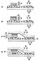
図1に本実施の形態の電子装置であるRFIDタグ用インレットの一例であり、ダイポールアンテナにIC素子を実装したインレットの概略図を示す。図1(a)は上面から見た概略図であり、図1(b)はA−A’部の断面概略図である。前記IC素子10には、珪素からなるベース基板11と、ベース基板11面の一方の面に形成された半導体回路層12と、この半導体回路層12上に電極13が各々形成されている。前記IC素子10は電極13によって、異方導電性接着剤層40に含有される導電粒子41を介して、アンテナとして動作する第一の回路層20に接続されている。また、前記IC素子10はベース基板11の他方の面によって、異方導電性接着剤層40に含有される導電粒子41を介して同じくアンテナとして動作する第二の回路層30に接続されている。IC素子10の電極13は第一の回路層20と、ベース基板11は第二の回路層30と、それぞれ電気的に接続されている。 FIG. 1 shows an example of an RFID tag inlet which is an electronic device of the present embodiment, and shows a schematic view of an inlet in which an IC element is mounted on a dipole antenna. FIG. 1A is a schematic view seen from above, and FIG. 1B is a schematic cross-sectional view of the A-A ′ portion. In the
また、本発明における電子装置は、一つの面に電極13が形成され、その対向する面が珪素からなるベース基板11であるIC素子10と、スリットが形成され、送受信アンテナとして動作する第一の回路層20と、前記IC素子10と前記第一の回路層20とを電気的に接続する短絡板として動作する第二の回路層30と、を含むものである。 In the electronic device according to the present invention, the
励振スリットを有するダイポールアンテナ構造は、このスリットの幅及び長さを変えることで、アンテナのインピーダンスと上記IC素子10の入力インピーダンスを整合することが可能であり、良好な通信特性を得るのに好適な構造である。 The dipole antenna structure having the excitation slit can match the impedance of the antenna and the input impedance of the
図2に本実施の形態の電子装置であるRFIDタグ用インレットの一例であり、励振スリット型ダイボールアンテナにIC素子10を実装したサンドイッチ・アンテナ構造をもつインレットを示す。図2(a)はこのインレットを上面から見た概略図であり、図2(b)は図2(a)のB−B’部の断面概略図である。この図2を用いて、前記インレットの構造を簡単に説明する。 FIG. 2 shows an example of an RFID tag inlet which is an electronic device according to the present embodiment, and shows an inlet having a sandwich antenna structure in which an
IC素子10には、図1(b)に示した例と同様に、珪素からなるベース基板11と、ベース基板11面上に形成された半導体回路層12と、半導体回路層12上に形成された電極13が各々形成されている。前記IC素子10は電極13によって、ベース基材22及びアンテナ回路21で構成され、第一の回路層20に第1の接続部2において、異方導電性接着剤層40に含有される導電粒子41を介して接続されている。同様に、ベース基材32及び導電層31で構成され、第二の回路層30と前記IC素子10のベース基板11が第2の接続部3において、また、第二の回路層30と第一の回路層20が第3の接続部4において、異方導電性接着剤層40に含有される導電粒子41を介して各々接続されている。前記IC素子10のベース基板11の第2の接続部3と第一の回路層20上の第3の接続部4は、第一の回路層20に形成されたスリット1を跨いで接続される構造となる。すなわち、前記IC素子10の電極13とベース基板11は、第1の接続部2、アンテナ回路21、第3の接続部4、第二の回路層30の導電層31及び第2の接続部3を介して電気的に接続される。また、第一の回路層20と第二の回路層30の空隙は、異方導電性接着剤層40のマトリクス樹脂42によって封止されている。なお、図2ではIC素子10のベース基板11が第二の回路層30の導電層31と、電極13がアンテナ回路21と接続された構造を示したが、IC素子10のベース基板11と電極13が反転した構造であっても、インレットとしての性能に変わりはない。 As in the example shown in FIG. 1B, the
次に、サンドイッチ・アンテナ構造をもつRFIDタグ用インレットの製造方法について例を挙げて説明する。 Next, a manufacturing method of an RFID tag inlet having a sandwich antenna structure will be described with an example.
本発明における前記電子装置の製造方法の第1の例は、金属箔を用いてアンテナ回路を形成する工程及びベース基材上に前記アンテナ回路を設けることで第一の回路層を形成する工程もしくはベース基材上に設けた金属箔からアンテナ回路を設けることで前記第一の回路層を形成する工程、前記アンテナ回路上のIC素子搭載部及び第二の回路層との接続部に第1の導電性接着剤層もしくは異方導電性接着剤層を形成する工程、前記第一の回路層のアンテナ回路上にIC素子を位置合せし仮固定する工程、前記IC素子上に第2の導電性接着剤層もしくは異方導電性接着剤を形成する工程、仮固定した前記IC素子及び前記第一の回路層のアンテナ回路上の所定の位置に電気的に接続するように導電層を形成した前記第二の回路層を位置合せする工程、前記第二の回路層を前記IC素子及び第一の回路層上に第2の導電性接着剤層もしくは異方導電性接着剤層を介して一括して加熱圧着する工程、を少なくとも有するものである。 The first example of the method of manufacturing the electronic device according to the present invention includes a step of forming an antenna circuit using a metal foil and a step of forming the first circuit layer by providing the antenna circuit on a base substrate. A step of forming the first circuit layer by providing an antenna circuit from a metal foil provided on the base substrate, and a first connection portion between the IC element mounting portion and the second circuit layer on the antenna circuit. A step of forming a conductive adhesive layer or an anisotropic conductive adhesive layer, a step of positioning and temporarily fixing an IC element on the antenna circuit of the first circuit layer, a second conductive property on the IC element The step of forming an adhesive layer or an anisotropic conductive adhesive, the conductive layer formed so as to be electrically connected to a predetermined position on the antenna circuit of the temporarily fixed IC element and the first circuit layer Align second circuit layer At least a step of thermocompression-bonding the second circuit layer on the IC element and the first circuit layer together via a second conductive adhesive layer or an anisotropic conductive adhesive layer. It is what you have.
また、本発明における前記電子装置の製造方法の第2の例は、金属箔を用いてアンテナ回路を形成する工程及びベース基材上に前記アンテナ回路を設けることで第一の回路層を形成する工程もしくはベース基材上に設けた金属箔からアンテナ回路を設けることで前記第一の回路層を形成する工程、前記第一の回路層のアンテナ回路上のIC素子搭載部に第1の導電性接着剤層もしくは異方導電性接着剤層を形成する工程、前記第一の回路層のアンテナ回路上にIC素子を位置合せし仮固定する工程、前記IC素子上に第2の導電性接着剤もしくは異方導電性接着剤層を形成する工程、仮固定した前記IC素子及び前記第一の回路層のアンテナ回路上の所定の位置に電気的に接続するように導電層を形成した第二の回路層を位置合せする工程、前記第二の回路層を前記IC素子上に第2の導電性接着剤層もしくは異方導電性接着剤層を介して加熱圧着する工程、前記第一の回路層のアンテナ回路の所定の位置に前記第二の回路層を超音波を印加しながら圧着する工程、を少なくとも有するものである。 According to a second example of the method for manufacturing the electronic device of the present invention, a first circuit layer is formed by forming an antenna circuit using a metal foil and providing the antenna circuit on a base substrate. A step of forming the first circuit layer by providing an antenna circuit from a metal foil provided on the step or the base substrate; a first conductive layer on the IC element mounting portion on the antenna circuit of the first circuit layer; A step of forming an adhesive layer or an anisotropic conductive adhesive layer, a step of aligning and temporarily fixing an IC element on the antenna circuit of the first circuit layer, and a second conductive adhesive on the IC element Alternatively, a step of forming an anisotropic conductive adhesive layer, a second layer in which a conductive layer is formed so as to be electrically connected to a predetermined position on the antenna circuit of the temporarily fixed IC element and the first circuit layer. Aligning circuit layers, A step of heat-pressing the second circuit layer on the IC element via a second conductive adhesive layer or an anisotropic conductive adhesive layer, and at a predetermined position of the antenna circuit of the first circuit layer; And a step of pressure-bonding the second circuit layer while applying an ultrasonic wave.
また、本発明における前記電子装置の製造方法の第3の例は、金属箔を用いてアンテナ回路を形成する工程及びベース基材上に前記アンテナ回路を設けることで第一の回路層を形成する工程もしくはベース基材上に設けた金属箔からアンテナ回路を設けることで前記第一の回路層を形成する工程、前記第一の回路層のアンテナ回路上のIC素子搭載部に第1の導電性接着剤層もしくは異方導電性接着剤層を形成する工程、前記第一の回路層のアンテナ回路上にIC素子を位置合せし仮固定する工程、前記IC素子上に第2の導電性接着剤もしくは異方導電性接着剤層を形成する工程、仮固定した前記IC素子及び前記第一の回路層のアンテナ回路上の所定の位置に電気的に接続するように導電層を形成した第二の回路層を位置合せする工程、前記第二の回路層を前記IC素子上に第2の導電性接着剤層もしくは異方導電性接着剤層を介して加熱圧着する工程、前記第一の回路層のアンテナ回路の所定の位置に前記第二の回路層を複数の針状の突起を有する治具にて機械的に圧接する工程、を少なくとも有するものである。 According to a third example of the method for manufacturing an electronic device of the present invention, a first circuit layer is formed by forming an antenna circuit using a metal foil and providing the antenna circuit on a base substrate. A step of forming the first circuit layer by providing an antenna circuit from a metal foil provided on the step or the base substrate; a first conductive layer on the IC element mounting portion on the antenna circuit of the first circuit layer; A step of forming an adhesive layer or an anisotropic conductive adhesive layer, a step of aligning and temporarily fixing an IC element on the antenna circuit of the first circuit layer, and a second conductive adhesive on the IC element Alternatively, a step of forming an anisotropic conductive adhesive layer, a second layer in which a conductive layer is formed so as to be electrically connected to a predetermined position on the antenna circuit of the temporarily fixed IC element and the first circuit layer. Aligning circuit layers, A step of heat-pressing the second circuit layer on the IC element via a second conductive adhesive layer or an anisotropic conductive adhesive layer, and at a predetermined position of the antenna circuit of the first circuit layer; At least a step of mechanically pressing the second circuit layer with a jig having a plurality of needle-like protrusions.
前記第1〜第3の例において、IC素子の電極及びベース基板のうちのどちらが第一の回路層と接続しても、また、電極及びベース基板の面方向に回転しても電子装置としての性能に変わりはなく、前記IC素子を特定の方向に並べる必要がないため、本発明の構造は大量生産を実現する上で好適である。 In the first to third examples, an electronic device can be formed by either the electrode of the IC element or the base substrate connected to the first circuit layer or rotating in the surface direction of the electrode or the base substrate. Since the performance does not change and the IC elements do not need to be arranged in a specific direction, the structure of the present invention is suitable for realizing mass production.
前記第1〜第3の例において、少なくともIC素子のベース基板の接続部は、導電接着剤もしくは異方導電性接着剤を介して形成される。前記導電性接着剤は熱硬化性のマトリクス樹脂と、粒状もしくはりん片状もしくは針状の金属片を含有する。また、前記異方導電性接着剤はマトリクス樹脂と、金属粒子もしくは表面に金属層が形成された有機樹脂粒子からなる導電性粒子を含有する。IC素子と第一及び第二の回路層を加熱圧着する際に、マトリクス樹脂中に含有される金属片もしくは導電性粒子がIC素子の珪素からなるベース基板に密着した状態で固定されるため、良好な電気的接続を得ることができる。 In the first to third examples, at least the connection portion of the base substrate of the IC element is formed via a conductive adhesive or an anisotropic conductive adhesive. The conductive adhesive contains a thermosetting matrix resin and granular, flake-like, or needle-like metal pieces. The anisotropic conductive adhesive contains matrix resin and conductive particles made of metal particles or organic resin particles having a metal layer formed on the surface. When the IC element and the first and second circuit layers are thermocompression bonded, the metal pieces or conductive particles contained in the matrix resin are fixed in close contact with the base substrate made of silicon of the IC element. Good electrical connection can be obtained.
異方導電性接着剤を介して接続を行う場合には、IC素子を第一及び第二の回路層と加熱圧着することによって電気的接続を行うとともに、第一及び第二の回路層の空隙を封止することができる。この場合、異方導電性接着剤層の厚みの合計を少なくとも前記IC素子の厚みの2分の1以上にすることが、第一及び第二の回路層との封止性を得ることができ、高信頼性を実現する点で好ましい。 When connecting via an anisotropic conductive adhesive, the IC element is electrically connected to the first and second circuit layers by thermocompression bonding, and the gap between the first and second circuit layers Can be sealed. In this case, by making the total thickness of the anisotropic conductive adhesive layer at least one half or more of the thickness of the IC element, sealing performance with the first and second circuit layers can be obtained. It is preferable in terms of realizing high reliability.
前記第1〜第3の例において、第一の回路層のアンテナ回路を形成する金属箔及び第二の回路層を形成する導電層の少なくとも一方はアルミニウムもしくは銅である。 In the first to third examples, at least one of the metal foil forming the antenna circuit of the first circuit layer and the conductive layer forming the second circuit layer is aluminum or copper.
前記第1〜第3の例において、第一及び第二の回路層の第1及び第2の金属箔の少なくとも一方は有機樹脂又は紙からなるベース基材に支持されている。前記有機樹脂は、塩化ビニル樹脂(PVC)、アクリロニトリルブタジエンスチレン(ABS)、ポリエチレンテレフタレート(PET)、グリコール変性ポリエチレンテレフタレート(PETG)、ポリエチレンナフタレート(PEN)、ポリカーボネート樹脂(PC)、2軸延伸ポリエステル(O−PET)、ポリイミド樹脂から選択される。 In the first to third examples, at least one of the first and second metal foils of the first and second circuit layers is supported by a base substrate made of organic resin or paper. The organic resin is vinyl chloride resin (PVC), acrylonitrile butadiene styrene (ABS), polyethylene terephthalate (PET), glycol-modified polyethylene terephthalate (PETG), polyethylene naphthalate (PEN), polycarbonate resin (PC), biaxially stretched polyester (O-PET) or polyimide resin.
前記第1〜第3の例において、第一の回路層を形成する方法としては、例えば、金属箔を用いてアンテナ回路を形成してからベース基材上に設けることで第一の回路層を形成する方法、ベース基材上に金属箔を設けてからエッチング等によりアンテナ回路を形成することで第一の回路層を形成する方法がある。 In the first to third examples, as a method of forming the first circuit layer, for example, an antenna circuit is formed using a metal foil and then the first circuit layer is provided on the base substrate. There is a method of forming a first circuit layer by forming a metal foil on a base substrate and then forming an antenna circuit by etching or the like.
前記第1〜第3の例において、第二の回路層を形成するために導電層をベース基材上に設ける方法としては、例えば、金属箔を単に前記ベース基材上に貼り付けるだけの方法があり、前記金属箔についてエッチング等の処理をする必要がないことから、低コスト化することができる点で好ましい。 In the first to third examples, as a method of providing the conductive layer on the base substrate to form the second circuit layer, for example, a method of simply attaching a metal foil on the base substrate Since the metal foil does not need to be processed such as etching, it is preferable in that the cost can be reduced.
前記第1〜第3の例において、図1におけるA−A’方向を幅方向としたとき、第二の回路層はスリットを跨いで前記IC素子にかかる程度の長さを有することが必要であり、アンテナ回路の幅とほぼ同等の長さを有していることがインレット全体の外観上好ましい。 In the first to third examples, when the AA ′ direction in FIG. 1 is the width direction, the second circuit layer needs to have a length that covers the IC element across the slit. In addition, it is preferable in terms of the appearance of the entire inlet that it has a length substantially equal to the width of the antenna circuit.
前記第1〜第3の例において、前記各工程を経て、本発明の電子装置であるインレット構造を得ることができる。 In the first to third examples, an inlet structure which is an electronic device of the present invention can be obtained through the above steps.
前記インレットについて、RFIDタグの形態で使用する際には、インレットの上下にカバーシートを設けることが、回路を保護してショート等を防ぐ点で好ましい。 When the inlet is used in the form of an RFID tag, it is preferable to provide cover sheets above and below the inlet from the viewpoint of protecting the circuit and preventing a short circuit or the like.
前記第1〜第3の例において、前記IC素子と第二の回路層を用い、スリットを跨ぐ接続構造とすることで、前記IC素子とアンテナ回路上の励振スリットの高精度な位置合せが不要であるため、複数の前記IC素子を例えば篩いや金型を用いて整列するような粗い位置精度でも、一括して第一の回路層に良好に実装することができる。即ち、前記IC素子を1個ずつ実装する場合に比べて優れた生産性を実現することができる。生産性を向上することでインレット1個当たりのタクト時間を短縮することができる。 In the first to third examples, the IC element and the second circuit layer are used, and the connection structure straddling the slit eliminates the need for highly accurate alignment of the IC element and the excitation slit on the antenna circuit. For this reason, the plurality of IC elements can be satisfactorily mounted on the first circuit layer even with a rough positional accuracy such that the plurality of IC elements are aligned using, for example, a sieve or a mold. That is, it is possible to realize superior productivity as compared with the case where the IC elements are mounted one by one. By improving productivity, the tact time per inlet can be shortened.
前記第1〜第3の例において、前記IC素子と第二の回路層を用い、スリットを跨ぐ接続構造を形成するために、導電性接着剤もしくは異方導電性接着剤層を介して接続を行うために、前記IC素子の珪素からなるベース基板上に金等を用いて電極を形成する必要がなく、低コスト化を実現できる。 In the first to third examples, the IC element and the second circuit layer are used, and a connection is formed via a conductive adhesive or an anisotropic conductive adhesive layer to form a connection structure straddling the slit. Therefore, it is not necessary to form an electrode using gold or the like on the base substrate made of silicon of the IC element, and cost reduction can be realized.
前記第1〜第3の例において、前記IC素子と第一及び第二の回路層の電気的接続は、導電性接着剤もしくは異方導電性接着剤層を介して行い、また、第一及び第二の回路層の電気的接続は、導電性接着剤もしくは異方導電性接着剤層を介した接続、もしくは超音波を印加して行う接続、もしくは複数の針状の突起を有する治具を用いた機械的圧接にて行うため、アンテナ回路上の表面めっきが不要であること、かつ、金属接合を形成するために200℃以上の高温でのボンディングに耐えうる高耐熱性ベース基材が不要であることから、安価なベース基材及びアンテナ回路の使用が可能となり、低コスト化を実現することができる。 In the first to third examples, the electrical connection between the IC element and the first and second circuit layers is performed through a conductive adhesive or an anisotropic conductive adhesive layer. The electrical connection of the second circuit layer can be made through a conductive adhesive or anisotropic conductive adhesive layer, a connection made by applying ultrasonic waves, or a jig having a plurality of needle-like protrusions. Since the mechanical pressure welding is used, surface plating on the antenna circuit is not necessary, and a high heat-resistant base substrate that can withstand bonding at a high temperature of 200 ° C. or higher is not necessary for forming a metal joint. Therefore, it is possible to use an inexpensive base substrate and antenna circuit, and it is possible to realize cost reduction.
例えば、従来の金−錫接合等で接続する場合には第一の回路層のベース基材として耐熱性の高いポリイミドを使用する必要があったのに対し、例えば、安価なポリエチレンテレフタレート等を使用することができる。また、前記接続部のアンテナ回路上の表面に錫めっき等を施す必要がないことから、錫やはんだのめっき性が悪いものの安価なアルミニウムをアンテナ回路の材料に使用することができる。従って、例えば、ポリエチレンテレフタレートのベース基材にアルミニウムのアンテナ回路を形成して得られる第一の回路層は、安価なRFIDタグ用インレットを製造するために好適な部材である。 For example, when connecting with a conventional gold-tin joint, etc., it was necessary to use polyimide with high heat resistance as the base substrate of the first circuit layer, for example, using inexpensive polyethylene terephthalate, etc. can do. Moreover, since it is not necessary to apply tin plating or the like to the surface of the connection portion on the antenna circuit, inexpensive aluminum can be used as the antenna circuit material, although tin or solder plating ability is poor. Therefore, for example, the first circuit layer obtained by forming an aluminum antenna circuit on a polyethylene terephthalate base substrate is a suitable member for manufacturing an inexpensive RFID tag inlet.
即ち、本発明の電子装置は、IC素子と、スリットが形成された送受信アンテナとして動作する第一の回路層と、前記IC素子と前記アンテナとを電気的に接続する短絡板として動作する第二の回路層とを含む電子装置において、前記IC素子は珪素からなるベース基板と、ベース基板上に半導体回路が形成された半導体回路層と、半導体回路層上に形成された電極とを有し、向かい合った1組の各々の面に位置する前記電極(ベース基板の一方の面)及び前記ベース基板面(ベース基板の他方の面)のうちの一方が前記第一の回路層と電気的に接続し、残るもう一方が前記第二の回路層と電気的に接続していることを特徴とする電子装置である。 That is, the electronic device of the present invention includes an IC element, a first circuit layer that operates as a transmission / reception antenna having a slit, and a second circuit that operates as a short-circuit plate that electrically connects the IC element and the antenna. In the electronic device including the circuit layer, the IC element includes a base substrate made of silicon, a semiconductor circuit layer in which a semiconductor circuit is formed on the base substrate, and an electrode formed on the semiconductor circuit layer, One of the electrode (one surface of the base substrate) and the base substrate surface (the other surface of the base substrate) located on each of the faces of the set facing each other is electrically connected to the first circuit layer. And the other is electrically connected to the second circuit layer.
前記第1〜第3の例で説明したように、少なくとも前記IC素子の珪素からなるベース基板面と第一及び第二の回路層との電気的接続部が導電性接着剤もしくは異方導電性接着剤を介して行われることによって、インレットが低コストで生産できるとともに、その生産性を飛躍的に向上することができる。 As described in the first to third examples, at least the electrical connection portion between the base substrate surface made of silicon of the IC element and the first and second circuit layers is a conductive adhesive or anisotropic conductive material. By being performed through the adhesive, the inlet can be produced at low cost, and the productivity can be dramatically improved.
以下、本発明の好適な実施例について図面を用いてさらに詳細に説明するが、本発明はこれらの実施例に限定されるものではない。 Hereinafter, preferred embodiments of the present invention will be described in more detail with reference to the drawings. However, the present invention is not limited to these embodiments.
<第1の実施の形態>
以下、図3を用いて、第1の実施の形態を説明する。<First Embodiment>
Hereinafter, the first embodiment will be described with reference to FIG.
まず、図3(a)に示すように、厚み50μmのポリエチレンテレフタレートによるベース基材22に、厚み9μmのアルミニウム箔を接着剤にて貼り合わせたテープ状基材のアルミニウム箔面に、スクリーン印刷でエッチングレジストを形成した後、エッチング液に塩化第二鉄水溶液を用いて、アンテナ回路21を形成し、第一の回路層10を作成する。ここで、アンテナ回路21のアンテナ幅を2.5mm、スリット幅を0.5mmとした。図は以下の工程を含めて、図2のB−B’で切断した場合の断面を示す。 First, as shown in FIG. 3 (a), screen printing is performed on an aluminum foil surface of a tape-like base material in which an aluminum foil having a thickness of 9 μm is bonded to a
次に、図3(b)に示すように、アンテナ回路21上の所定の位置に、幅2mmの異方導電性接着フィルム40(AC−2052P−45(日立化成工業(株)製))を80℃でラミネートし、セパレータフィルムを剥がして異方導電性接着剤層40を形成した。 Next, as shown in FIG. 3B, an anisotropic conductive
次に、図3(c)に示すように、IC素子10をアンテナ回路21上の所定の位置に位置合せし、仮固定した。図には電極13がアンテナ回路21面に対向するように示したが、上下を反転しベース基板11がアンテナ回路21面に対向するように仮固定しても差し支えはない。 Next, as shown in FIG. 3C, the
次に、図3(d)に示すように、厚み50μmのポリエチレンテレフタレートによるベース基材32に、厚み9μmのアルミニウム箔を接着剤にて貼り合わせた、幅2mmのテープ状基材のアルミニウム箔面上に、前記テープ基材と同幅の前記異方導電性接着フィルム400を80℃でラミネートし、セパレータフィルムを剥がし、異方導電性接着剤層40付き第二の回路層30とした後、前記異方導電性接着剤層40がIC素子10に対向する向きで、第一の回路層20と所定の位置に合せ、仮固定した。 Next, as shown in FIG. 3 (d), an aluminum foil surface of a tape-like substrate having a width of 2 mm, in which an aluminum foil having a thickness of 9 μm is bonded to a
次に、図3(e)に示すように、異方導電性接着材層40付き第二の回路層30側から圧着ヘッドを降下し、圧力12MPa、温度180℃、加熱時間15秒の条件で、前記異方導電性接着剤層40付き第二の回路層30を第一の回路層20の前記IC素子10及びアンテナ回路21に対して所定の位置に一括して加熱圧着するとともに、第一の回路層20と第二の回路層30との空隙を封止した。圧着ヘッドには、前記IC素子10と第一の回路層20及び第二の回路層30の接続と、第一の回路層20及び第二の回路層30の接続が同時にできるように、前記IC素子10の厚み分の突起を所定の位置に形成してある。 Next, as shown in FIG. 3 (e), the pressure-bonding head is lowered from the
以上の工程にて、図2及び図3(e)に示す形状のインレットを得た。また、通信試験を行った結果、通信不良はなかった。 Through the above steps, an inlet having the shape shown in FIGS. 2 and 3E was obtained. As a result of the communication test, there was no communication failure.
本工程を用いれば、IC素子10の珪素からなるベース基板11(前記他方の面)上に電極を形成する必要がないため、良好な通信特性をもつインレットを低コストで実現することができる。 If this step is used, it is not necessary to form an electrode on the base substrate 11 (the other surface) made of silicon of the
<第2の実施の形態>
以下、図4を用いて、第2の実施の形態を説明する。<Second Embodiment>
Hereinafter, the second embodiment will be described with reference to FIG.
まず、図4(a)に示すように、図3(c)までは第1の実施の形態と同様の工程を用いて、前記第一の回路層20の加工を行い、前記異方導電性接着フィルムをアンテナ回路上にラミネートして異方導電性接着剤層40を形成し、アンテナ回路21上の所定の位置に、前記IC素子10を仮固定した。 First, as shown in FIG. 4A, the
次に、図4(b)に示すように、前記IC素子10のアンテナ回路21に対向する面とは反対面上に銀フィラー含有導電性接着剤50を塗布した。 Next, as shown in FIG. 4B, a silver filler-containing conductive adhesive 50 was applied on the surface opposite to the surface facing the
次に、図4(c)に示すように、厚み50μmのポリエチレンテレフタレートによるベース基材32に、厚み9μmのアルミニウム箔を接着剤にて貼り合わせて導電層31とし、幅2mmのテープ状の第二の回路層30とした後、前記アルミニウム箔による導電層31がIC素子10に対向する向きで、第一の回路層20と所定の位置に合せ、仮固定した。 Next, as shown in FIG. 4C, an aluminum foil having a thickness of 9 μm is bonded to a
次に、図4(d)に示すように、第二の回路層30側から圧着ヘッドを降下し、圧力12MPa、温度180℃、加熱時間15秒の条件で、前記第二の回路層30を第一の回路層20の前記IC素子10及びアンテナ回路21に対して所定の位置に一括して加熱圧着するとともに、第一の回路層20と第二の回路層30との空隙を封止した。圧着ヘッドには、前記IC素子10と第一の回路層20及び第二の回路層30の接続と、第一の回路層20及び第二の回路層30の接続が同時にできるように、前記IC素子10の厚み分の突起を所定の位置に形成してある。 Next, as shown in FIG. 4D, the crimping head is lowered from the
以上の工程にて、図2及び図4(d)に示す形状のインレットを得た。また、通信試験を行った結果、通信不良はなかった。 Through the above steps, an inlet having the shape shown in FIGS. 2 and 4D was obtained. As a result of the communication test, there was no communication failure.
本工程を用いれば、第1の実施の形態と同様に、IC素子10の珪素からなるベース基板11(前記他方の面)上に電極を形成する必要がないため、良好な通信特性をもつインレットを低コストで実現することができる。 If this step is used, it is not necessary to form an electrode on the base substrate 11 (the other surface) made of silicon of the
<第3の実施の形態>
以下、図5を用いて、第3の実施の形態を説明する。<Third Embodiment>
Hereinafter, the third embodiment will be described with reference to FIG.
まず、図5(a)に示すように、図3(c)までは第1の実施の形態と同様の工程を用いて、前記第一の回路層20の加工を行い、前記異方導電性接着フィルムをアンテナ回路21上のIC素子10の実装位置の近傍の所定の位置にラミネートして異方導電性接着剤層40を形成し、アンテナ回路21上の所定の位置に、前記IC素子10を仮固定した。 First, as shown in FIG. 5A, the
次に、図5(b)に示すように、図3(d)と同様の工程を用いて、異方導電性接着剤層40をIC素子10の接続位置の近傍の所定の場所に形成した異方導電性接着剤層40付き第二の回路層30を準備した後、前記異方導電性接着剤層40がIC素子10に対向する向きで、第一の回路層20と所定の位置に合せ、仮固定した。 Next, as shown in FIG. 5B, the anisotropic conductive
次に、図5(c)に示すように、第二の回路層30側から圧着ヘッドを降下し、圧力12MPa、温度180℃、加熱時間15秒の条件で、前記第二の回路層30を第一の回路層20の前記IC素子10に対して所定の位置に一括して加熱圧着するとともに、第一の回路層20と第二の回路層30との間のIC素子10の近傍を封止した。 Next, as shown in FIG. 5C, the pressure-bonding head is lowered from the
次に、図5(d)に示すように、第二の回路層30と第一の回路層20の接続部に、第二の回路層30側から超音波接合ヘッド110を降下し、出力1Wの超音波振動を圧力12MPa、温度180℃、印加時間1秒の条件で印加しながら、超音波接合を行った。 Next, as shown in FIG. 5D, the
以上の工程にて、図2及び図5(d)に示す形状のインレットを得た。また、通信試験を行った結果、通信不良はなかった。 Through the above steps, an inlet having the shape shown in FIGS. 2 and 5D was obtained. As a result of the communication test, there was no communication failure.
本工程を用いれば、第1及び第2の実施の形態と同様に、IC素子10の珪素からなるベース基板11上(前記他方の面)に電極を形成する必要がないため、良好な通信特性をもつインレットを低コストで実現することができる。 If this step is used, it is not necessary to form an electrode on the base substrate 11 (the other surface) made of silicon of the
<第4の実施の形態>
以下、図6を用いて、第4の実施の形態を説明する。<Fourth embodiment>
Hereinafter, the fourth embodiment will be described with reference to FIG.
まず、図6(a)に示すように、図5(c)までは第3の実施の形態と同様の工程を用いて、第一の回路層20の加工、異方導電性接着剤層40の形成、アンテナ回路21上の所定の位置へのIC素子10を仮固定、異方導電性接着剤層40付き第二の回路層30の準備及び第一の回路層20への仮固定、第二の回路層30の加熱圧着を順次行った。 First, as shown in FIG. 6A, processing up to the
次に、図6(b)に示すように、第一の回路層20と第二の回路層30の接続部を、多数の針状の凹凸をもつ一組のかしめ治具120を用いて圧接を行った。圧接によって第一の回路層20と第二の回路層30のアルミニウム箔同士が塑性変形を起こし、機械的に接触した状態で固定され、電気的接続が得られる。すなわち、第一の回路層20のアンテナ回路21と第二の回路層30の導電層31が電気的に接続する。 Next, as shown in FIG. 6 (b), the connecting portion of the
以上の工程にて、図2及び図6に示す形状のインレットを得た。また、通信試験を行った結果、通信不良はなかった。 Through the above steps, an inlet having the shape shown in FIGS. 2 and 6 was obtained. As a result of the communication test, there was no communication failure.
本工程を用いれば、第1〜第3の実施の形態と同様に、IC素子10の珪素からなるベース基板11上(前記他方の面)に電極を形成する必要がないため、良好な通信特性をもつインレットを低コストで実現することができる。 If this step is used, it is not necessary to form an electrode on the base substrate 11 (the other surface) made of silicon of the
以上の実施例の結果をまとめて表1に示す。

Claims (6)
前記IC素子は、珪素からなるベース基板と、前記ベース基板の一方の面に半導体回路が形成された半導体回路層と、前記半導体回路層上に形成された電極とを有し、前記ベース基板の他方の面には電極を有しておらず、
前記第一の回路層が前記ベース基板の他方の面又は前記電極のいずれか一方と、前記第二の回路層が前記ベース基板の他方の面又は前記電極の残る一方と、それぞれ電気的に接続され、
前記ベース基板の他方の面及び前記電極は何れも、加熱圧着することによって前記第一及び第二の回路層の空隙を封止する異方導電性接着剤を介して、前記第一又は第二の回路層と電気的に接続されることを特徴とする電子装置。In an electronic device including an IC element and first and second circuit layers that operate as either an antenna or a short circuit plate ,
The IC element includes a base substrate made of silicon, a semiconductor circuit layer in which a semiconductor circuit is formed on one surface of the base substrate, and an electrode formed on the semiconductor circuit layer. There is no electrode on the other side,
The first circuit layer is electrically connected to either the other surface of the base substrate or the electrode, and the second circuit layer is electrically connected to the other surface of the base substrate or the remaining electrode. And
The other surface of the base substrate and the electrode are both bonded to the first or second through an anisotropic conductive adhesive that seals the gap between the first and second circuit layers by thermocompression bonding. An electronic device characterized in that the electronic device is electrically connected to the circuit layer.
Applications Claiming Priority (3)
| Application Number | Priority Date | Filing Date | Title |
|---|---|---|---|
| JP2004030535 | 2004-02-06 | ||
| JP2004030535 | 2004-02-06 | ||
| PCT/JP2005/001486 WO2005076202A1 (en) | 2004-02-06 | 2005-02-02 | Electronic device |
Publications (2)
| Publication Number | Publication Date |
|---|---|
| JPWO2005076202A1 JPWO2005076202A1 (en) | 2007-08-02 |
| JP4518024B2 true JP4518024B2 (en) | 2010-08-04 |
Family
ID=34836004
Family Applications (1)
| Application Number | Title | Priority Date | Filing Date |
|---|---|---|---|
| JP2005517695A Expired - Fee Related JP4518024B2 (en) | 2004-02-06 | 2005-02-02 | Electronic equipment |
Country Status (7)
| Country | Link |
|---|---|
| US (1) | US20090065586A1 (en) |
| EP (1) | EP1715445A4 (en) |
| JP (1) | JP4518024B2 (en) |
| KR (1) | KR100879416B1 (en) |
| CN (1) | CN1918583B (en) |
| TW (1) | TW200527312A (en) |
| WO (1) | WO2005076202A1 (en) |
Families Citing this family (8)
| Publication number | Priority date | Publication date | Assignee | Title |
|---|---|---|---|---|
| FI7351U1 (en) * | 2006-09-19 | 2007-01-12 | Upm Kymmene Wood Oy | Wooden board |
| JP4434311B2 (en) | 2007-07-18 | 2010-03-17 | 株式会社村田製作所 | Wireless IC device and manufacturing method thereof |
| CN104246630B (en) * | 2012-04-11 | 2017-09-12 | 英频杰公司 | There is the RFID integrated circuits and label of antenna contacts on multiple surfaces |
| US10600753B2 (en) * | 2015-08-28 | 2020-03-24 | Texas Instruments Incorporated | Flip chip backside mechanical die grounding techniques |
| DE102016103790B8 (en) | 2016-03-03 | 2021-06-02 | Infineon Technologies Ag | Production of a package using a platable encapsulation material |
| EP3456161A1 (en) * | 2016-05-11 | 2019-03-20 | Flex Automotive GmbH | Electrical circuitry assembly and method for manufacturing the same |
| JP2019004266A (en) * | 2017-06-13 | 2019-01-10 | 富士通株式会社 | Antenna device and electronic apparatus |
| WO2020240252A1 (en) * | 2019-05-29 | 2020-12-03 | Stora Enso Oyj | Method and apparatus for producing a radio-frequency identification (rfid) transponder |
Citations (5)
| Publication number | Priority date | Publication date | Assignee | Title |
|---|---|---|---|---|
| JPH061096A (en) * | 1992-06-17 | 1994-01-11 | Omron Corp | Card-like substrate and manufacture thereof |
| WO2000076279A1 (en) * | 1999-06-03 | 2000-12-14 | Toyo Kohan Co.,Ltd. | Process for producing printed wiring board, ic card and printed wiring substrate |
| JP2001217380A (en) * | 2000-02-04 | 2001-08-10 | Hitachi Ltd | Semiconductor device and its manufacturing method |
| JP2002017614A (en) * | 2000-07-07 | 2002-01-22 | Toto Ltd | Toilet seat apparatus |
| JP2002366917A (en) * | 2001-06-07 | 2002-12-20 | Hitachi Ltd | Ic card incorporating antenna |
Family Cites Families (8)
| Publication number | Priority date | Publication date | Assignee | Title |
|---|---|---|---|---|
| US6459588B1 (en) * | 1998-07-08 | 2002-10-01 | Dai Nippon Printing Co., Ltd. | Noncontact IC card and fabrication method thereof |
| JP3398705B2 (en) * | 2000-02-24 | 2003-04-21 | 九州日本電気株式会社 | Semiconductor device |
| JP2002164392A (en) * | 2000-11-28 | 2002-06-07 | Toppan Forms Co Ltd | Method for mounting ic chip |
| US6407669B1 (en) * | 2001-02-02 | 2002-06-18 | 3M Innovative Properties Company | RFID tag device and method of manufacturing |
| JP2003076969A (en) * | 2001-08-31 | 2003-03-14 | Oji Paper Co Ltd | Ic chip mounting body |
| JP2003196631A (en) * | 2001-12-27 | 2003-07-11 | Toppan Forms Co Ltd | Ic media having bending resistance |
| JP2003228698A (en) * | 2002-02-04 | 2003-08-15 | Oji Paper Co Ltd | Non-contact ic card |
| US7015479B2 (en) * | 2003-07-31 | 2006-03-21 | Eastman Kodak Company | Digital film grain |
-
2005
- 2005-02-02 KR KR1020067017616A patent/KR100879416B1/en not_active IP Right Cessation
- 2005-02-02 EP EP05709607.5A patent/EP1715445A4/en not_active Withdrawn
- 2005-02-02 US US10/588,547 patent/US20090065586A1/en not_active Abandoned
- 2005-02-02 CN CN2005800040811A patent/CN1918583B/en not_active Expired - Fee Related
- 2005-02-02 JP JP2005517695A patent/JP4518024B2/en not_active Expired - Fee Related
- 2005-02-02 WO PCT/JP2005/001486 patent/WO2005076202A1/en active Application Filing
- 2005-02-04 TW TW094103689A patent/TW200527312A/en unknown
Patent Citations (5)
| Publication number | Priority date | Publication date | Assignee | Title |
|---|---|---|---|---|
| JPH061096A (en) * | 1992-06-17 | 1994-01-11 | Omron Corp | Card-like substrate and manufacture thereof |
| WO2000076279A1 (en) * | 1999-06-03 | 2000-12-14 | Toyo Kohan Co.,Ltd. | Process for producing printed wiring board, ic card and printed wiring substrate |
| JP2001217380A (en) * | 2000-02-04 | 2001-08-10 | Hitachi Ltd | Semiconductor device and its manufacturing method |
| JP2002017614A (en) * | 2000-07-07 | 2002-01-22 | Toto Ltd | Toilet seat apparatus |
| JP2002366917A (en) * | 2001-06-07 | 2002-12-20 | Hitachi Ltd | Ic card incorporating antenna |
Also Published As
| Publication number | Publication date |
|---|---|
| WO2005076202A1 (en) | 2005-08-18 |
| EP1715445A1 (en) | 2006-10-25 |
| JPWO2005076202A1 (en) | 2007-08-02 |
| CN1918583B (en) | 2011-06-15 |
| EP1715445A4 (en) | 2016-08-31 |
| CN1918583A (en) | 2007-02-21 |
| KR100879416B1 (en) | 2009-01-19 |
| KR20060126801A (en) | 2006-12-08 |
| US20090065586A1 (en) | 2009-03-12 |
| TWI295789B (en) | 2008-04-11 |
| TW200527312A (en) | 2005-08-16 |
Similar Documents
| Publication | Publication Date | Title |
|---|---|---|
| JP4737505B2 (en) | IC tag inlet and manufacturing method of IC tag inlet | |
| JP4518024B2 (en) | Electronic equipment | |
| KR20010072939A (en) | Ic card | |
| EP1769430A1 (en) | Rfid device and method of forming | |
| JP2000182017A (en) | Ic card used as contacing/noncontacting type and its manufacture | |
| JP4697228B2 (en) | Manufacturing method of electronic device | |
| JP4353181B2 (en) | Manufacturing method of electronic device | |
| JP2014135389A (en) | Flexible printed wiring board using metal base material film and non-contact ic card using flexible printed wiring board | |
| KR100846236B1 (en) | A smart card web and a method for its manufacture | |
| JP4386038B2 (en) | Manufacturing method of electronic device | |
| JP2000207519A (en) | Contact/noncontact type bifunctional ic card and its manufacture | |
| JP4449477B2 (en) | Electronic inlet | |
| JP3827014B2 (en) | Electromagnetic readable data carrier | |
| JP4529216B2 (en) | IC card and manufacturing method thereof | |
| JP2005347635A (en) | Semiconductor device | |
| JP2002304606A (en) | Non-contact communication medium and its manufacturing method |
Legal Events
| Date | Code | Title | Description |
|---|---|---|---|
| A131 | Notification of reasons for refusal |
Free format text: JAPANESE INTERMEDIATE CODE: A131 Effective date: 20090303 |
|
| A521 | Written amendment |
Free format text: JAPANESE INTERMEDIATE CODE: A523 Effective date: 20090507 |
|
| A131 | Notification of reasons for refusal |
Free format text: JAPANESE INTERMEDIATE CODE: A131 Effective date: 20090630 |
|
| A521 | Written amendment |
Free format text: JAPANESE INTERMEDIATE CODE: A523 Effective date: 20090826 |
|
| A02 | Decision of refusal |
Free format text: JAPANESE INTERMEDIATE CODE: A02 Effective date: 20091215 |
|
| A521 | Written amendment |
Free format text: JAPANESE INTERMEDIATE CODE: A523 Effective date: 20100311 |
|
| A911 | Transfer to examiner for re-examination before appeal (zenchi) |
Free format text: JAPANESE INTERMEDIATE CODE: A911 Effective date: 20100323 |
|
| TRDD | Decision of grant or rejection written | ||
| A01 | Written decision to grant a patent or to grant a registration (utility model) |
Free format text: JAPANESE INTERMEDIATE CODE: A01 Effective date: 20100427 |
|
| A01 | Written decision to grant a patent or to grant a registration (utility model) |
Free format text: JAPANESE INTERMEDIATE CODE: A01 |
|
| A61 | First payment of annual fees (during grant procedure) |
Free format text: JAPANESE INTERMEDIATE CODE: A61 Effective date: 20100510 |
|
| FPAY | Renewal fee payment (event date is renewal date of database) |
Free format text: PAYMENT UNTIL: 20130528 Year of fee payment: 3 |
|
| S531 | Written request for registration of change of domicile |
Free format text: JAPANESE INTERMEDIATE CODE: R313531 |
|
| S533 | Written request for registration of change of name |
Free format text: JAPANESE INTERMEDIATE CODE: R313533 |
|
| FPAY | Renewal fee payment (event date is renewal date of database) |
Free format text: PAYMENT UNTIL: 20130528 Year of fee payment: 3 |
|
| R350 | Written notification of registration of transfer |
Free format text: JAPANESE INTERMEDIATE CODE: R350 |
|
| FPAY | Renewal fee payment (event date is renewal date of database) |
Free format text: PAYMENT UNTIL: 20130528 Year of fee payment: 3 |
|
| LAPS | Cancellation because of no payment of annual fees |